

TL1593C
3-CHANNEL SAMPLE-AND-HOLD CIRCUIT
SOCS027B – APRIL 1987 – REVISED JULY 1991
Copyright 1991, Texas Instruments Incorporated
1
POST OFFICE BOX 655303 • DALLAS, TEXAS 75265
• Designed for Use With TI Virtual-Phase
CCD Image Sensors
• Supports Both Color and Monochrome
Applications
• Contains Three Separate Sample-and-Hold
Circuits
• Differential Input With 11-dB Gain
• 5-MHz Sampling Rate on Each Channel
• Separate Analog and Digital Supplies for
Immunity to Switching Transients
description
The TL1593C is a three-channel sample-and-hold integrated circuit designed for use in processing video
signals generated by TI virtual-phase CCD image sensors. It can be used with one-, two-, and three-channel
color and monochrome TI virtual-phase CCDs.
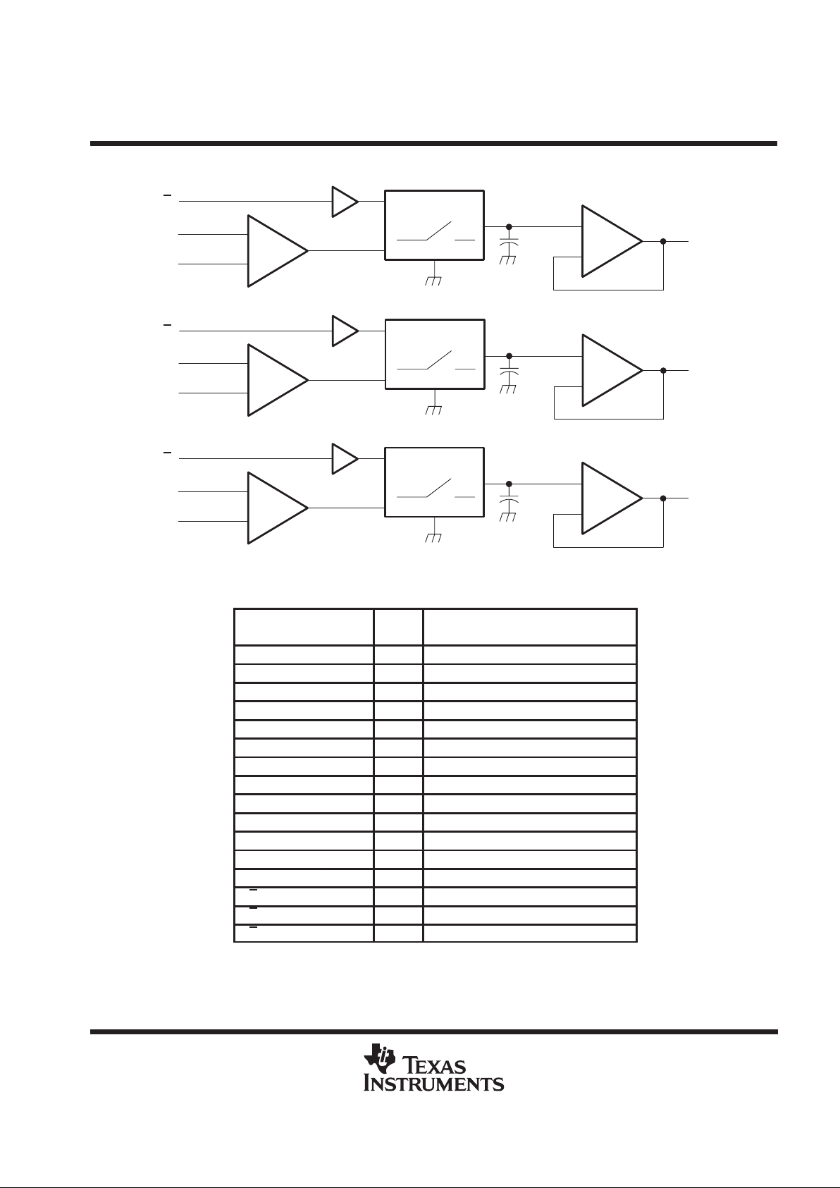
Each sample-and-hold channel consists of a differential-input buffer , a digitally controlled switch, and an output
buffer that has high impedance. Separate supply and ground pins are provided for the analog and digital
sections to ensure optimum isolation. Internal-hold capacitors are included to reduce the external parts count.
The differential inputs allow the amplifier return pin of the imager to be connected to CIN of the sample-and-hold
circuit to obtain common-mode rejection for antiblooming clock transients in the CCD. The analog inputs should
be capacitively coupled from the CCD outputs to ensure optimum performance.
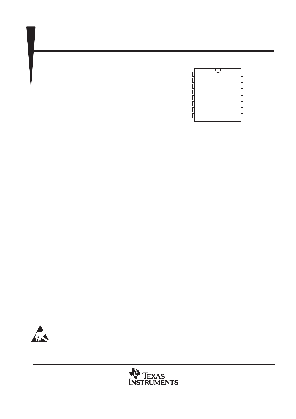
The TL1593C is supplied in a 16-pin plastic package and is characterized for operation from 0°C to 70°C.
This device contains circuits to protect its inputs and outputs against damage due to high static voltages or electrostatic fields. These
circuits have been qualified to protect this device against electrostatic discharges (ESD) of up to 2 kV according to MIL-STD-883C,
Method 3015; however, precautions should be taken to avoid application of any voltage higher than maximum-rated voltages to these
high-impedance circuits. During storage or handling, the device leads should be shorted together or the device should be placed in
conductive foam. In a circuit, unused inputs should always be connected to an appropriate logic voltage level, preferably either VCC or ground.
Specific guidelines for handling devices of this type are contained in the publication
Guidelines for Handling Electrostatic-Discharge-Sensitive
(ESDS) Devices and Assemblies
available from Texas Instruments.
1
2
3
4
5
6
7
8
16
15
14
13
12
11
10
9
ANLG V
CC
AIN1
CIN1
AIN2
CIN2
AIN3
CIN3
ANLG GND
S/H
1
S/H
2
S/H
3
DIG V
CC
OUT1
OUT2
OUT3
DIG GND
NS PACKAGE
(TOP VIEW)
PRODUCTION DATA information is current as of publication date.
Products conform to specifications per the terms of Texas Instruments
standard warranty. Production processing does not necessarily include
testing of all parameters.
TL1593C
3-CHANNEL SAMPLE-AND-HOLD CIRCUIT
SOCS027B – APRIL 1987 – REVISED JULY 1991
2
POST OFFICE BOX 655303 • DALLAS, TEXAS 75265
schematic
–
+
OUT1
2
3
11 dB
12
16
S/H1
CIN1
AIN1
–
+
DIG GND
ANLG
GND
–
+
OUT2
4
5
11 dB
11
15
–
+
S/H2
CIN2
AIN2
DIG GND
ANLG
GND
–
+
OUT3
6
7
11 dB
10
14
–
+
S/H3
CIN3
AIN3
DIG GND
ANLG
GND
Terminal Functions
TERMINAL
NAME NO.
I/O
DESCRIPTION
AIN1 2 I Channel 1 analog input
AIN2 4 I Channel 2 analog input
AIN3 6 I Channel 3 analog input
ANLG GND 8 Analog ground
ANLG V
CC
1 Analog supply voltage
CIN1 3 I Channel 1 compensation input
CIN2 5 I Channel 2 compensation input
CIN3 7 I Channel 3 compensation input
DIG GND 9 Digital ground
DIG V
CC
13 Digital supply voltage
OUT1 12 O Channel 1 output
OUT2 11 O Channel 2 output
OUT3 10 O Channel 3 output
S/H1 16 I Channel 1 sample-and-hold input
S/H2 15 I Channel 2 sample-and-hold input
S/H3 14 I Channel 3 sample-and-hold input

TL1593C
3-CHANNEL SAMPLE-AND-HOLD CIRCUIT
SOCS027B – APRIL 1987 – REVISED JULY 1991
3
POST OFFICE BOX 655303 • DALLAS, TEXAS 75265
absolute maximum ratings over operating free-air temperature range (unless otherwise noted)
†
Analog supply voltage range, ANLG V
CC
(see Note 1) –0.4 V to 16 V. . . . . . . . . . . . . . . . . . . . . . . . . . . . . . . . .
Digital supply voltage range, DIG V
CC
–0.4 V to 16 V. . . . . . . . . . . . . . . . . . . . . . . . . . . . . . . . . . . . . . . . . . . . . . .
Input voltage range, V
I
: AINn inputs –0.4 V to ANLG V
CC
. . . . . . . . . . . . . . . . . . . . . . . . . . . . . . . . . . . . . . . . . . .
CINn inputs –0.4 V to ANLG V
CC
. . . . . . . . . . . . . . . . . . . . . . . . . . . . . . . . . . . . . . . . . . .
S/H
n inputs –0.4 V to DIG V
CC
. . . . . . . . . . . . . . . . . . . . . . . . . . . . . . . . . . . . . . . . . . . . .
Continuous total power dissipation at (or below) T
A
≤ 25°C 625 mW. . . . . . . . . . . . . . . . . . . . . . . . . . . . . . . . . .
Operating free-air temperature range, T
A
30°C to 75°C. . . . . . . . . . . . . . . . . . . . . . . . . . . . . . . . . . . . . . . . . . . . .
Storage temperature range, T
STG
–55°C to 125°C. . . . . . . . . . . . . . . . . . . . . . . . . . . . . . . . . . . . . . . . . . . . . . . . .
Lead temperature 1,6 mm (1/16 inch) from case for 10 seconds 260°C. . . . . . . . . . . . . . . . . . . . . . . . . . . . . . .
†
Stresses beyond those listed under “absolute maximum ratings” may cause permanent damage to the device. These are stress ratings only, and
functional operation of the device at these or any other conditions beyond those indicated under “recommended operating conditions” is not
implied. Exposure to absolute-maximum-rated conditions for extended periods may affect device reliability.
NOTE 1: All voltage values are with respect to GND.
recommended operating conditions
MIN NOM MAX UNIT
Analog supply voltage, ANLG V
CC
10 12 13 V
Digital supply voltage, DIG V
CC
10 12 13 V
High-level input voltage, V
IH
2 V
Low-level input voltage, V
IL
0.8 V
p
AINn inputs 4.9 5.1 5.3
Input bias voltage, V
IB
CINn inputs 2.2 2.4 2.6
V
p
AINn inputs VIB – 0.3 VIBVIB + 0.3
Input voltage, V
I
CINn inputs VIB – 0.2 VIBVIB + 0.2
V
Sampling frequency 5 MHz
Sampling time 55 ns
Operating free-air temperature, T
A
30 75 °C
electrical characteristics over recommended ranges of supply voltage and operating free-air
temperature (unless otherwise noted)
PARAMETER TEST CONDITIONS MIN TYP‡MAX UNIT
Output voltage level 6 6.75 7.5 V
Output voltage swing 2 V
I
IH
High-level input current VI = 2.7 V, DIG VCC = 12 V 10 µA
I
IL
Low-level input current VI = 0.4 V, DIG VCC = 12 V –160 –300 µA
I
O–
Output source current –5 mA
I
O+
Output sink current 0.4 mA
I
CC
Supply current DIG VCC = 12 V, ANLG VCC = 12 V 18.5 28 mA
AINn inputs 5 7
C
i
Input capacitance CINn inputs 19 24 pF
S/Hn inputs 13 18
Input impedance AINn inputs 100 kΩ
Output impedance 50 200 Ω
‡
All typical values are at TA = 25° C.

TL1593C
3-CHANNEL SAMPLE-AND-HOLD CIRCUIT
SOCS027B – APRIL 1987 – REVISED JULY 1991
4
POST OFFICE BOX 655303 • DALLAS, TEXAS 75265
MECHANICAL DATA
NS/R-PDSO-G** PLASTIC SMALL-OUTLINE PACKAGE
8,20
7,40
5,00
5,60
0°–10°
0,10
0,20
1,05
0,55
0,40
4040062/A–10/93
16 9
18
A
2,00 MAX
0,05 MIN
PINS**
DIM
24
15,30
14,70
20
12,90
12,30
16
10,50
9,90
9,90A MIN
A MAX 10,50
14
16 PIN SHOWN
Seating Plane
0,10
1,27
M
0,25
NOTES: A. All linear dimensions are in millimeters.
B. This drawing is subject to change without notice.
C. Body dimensions do not include mold flash or protrusion not to exceed 0,15.

IMPORTANT NOTICE
T exas Instruments and its subsidiaries (TI) reserve the right to make changes to their products or to discontinue
any product or service without notice, and advise customers to obtain the latest version of relevant information
to verify, before placing orders, that information being relied on is current and complete. All products are sold
subject to the terms and conditions of sale supplied at the time of order acknowledgement, including those
pertaining to warranty, patent infringement, and limitation of liability.
TI warrants performance of its semiconductor products to the specifications applicable at the time of sale in
accordance with TI’s standard warranty. Testing and other quality control techniques are utilized to the extent
TI deems necessary to support this warranty. Specific testing of all parameters of each device is not necessarily
performed, except those mandated by government requirements.
CERT AIN APPLICATIONS USING SEMICONDUCTOR PRODUCTS MAY INVOLVE POTENTIAL RISKS OF
DEATH, PERSONAL INJURY, OR SEVERE PROPERTY OR ENVIRONMENTAL DAMAGE (“CRITICAL
APPLICATIONS”). TI SEMICONDUCTOR PRODUCTS ARE NOT DESIGNED, AUTHORIZED, OR
WARRANTED TO BE SUITABLE FOR USE IN LIFE-SUPPORT DEVICES OR SYSTEMS OR OTHER
CRITICAL APPLICATIONS. INCLUSION OF TI PRODUCTS IN SUCH APPLICA TIONS IS UNDERST OOD TO
BE FULLY AT THE CUSTOMER’S RISK.
In order to minimize risks associated with the customer’s applications, adequate design and operating
safeguards must be provided by the customer to minimize inherent or procedural hazards.
TI assumes no liability for applications assistance or customer product design. TI does not warrant or represent
that any license, either express or implied, is granted under any patent right, copyright, mask work right, or other
intellectual property right of TI covering or relating to any combination, machine, or process in which such
semiconductor products or services might be or are used. TI’s publication of information regarding any third
party’s products or services does not constitute TI’s approval, warranty or endorsement thereof.
Copyright 1998, Texas Instruments Incorporated
 Loading...