

Page 1
CHIP FORM
查询TL1454供应商
TL1454, TL1454Y
DUAL-CHANNEL PULSE-WIDTH-MODULATION (PWM)
CONTROL CIRCUIT
SLVS086B – APRIL 1995 – REVISED NOVEMBER 1997
D
Two Complete PWM Control Circuits
D
Outputs Drive MOSFETs Directly
D
Oscillator Frequency...50 kHz to 2 MHz
D
3.6-V to 20-V Supply-Voltage Range
D
Low Supply Current...3.5 mA Typ
D
Adjustable Dead-Time Control, 0% to 100%
D
1.25-V Reference
description
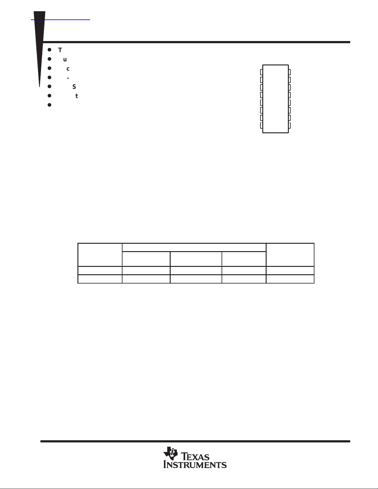
D, N OR PW PACKAGE
(TOP VIEW)
CT
1
RT
2
DTC1
IN1+
IN1–
COMP1
GND
OUT1
3
4
5
6
7
8
16
15
14
13
12
11
10
9
REF
SCP
DTC2
IN2+
IN2–
COMP2
V
CC
OUT2
The TL1454 is a dual-channel pulse-width-modulation (PWM) control circuit, primarily intended for
low-power, dc/dc converters. Applications include
LCD displays, backlight inverters, notebook computers, and other products requiring small, high-frequency , dc/dc converters. Each PWM channel has its own
error amplifier, PWM comparator, dead-time control comparator, and MOSFET driver. The voltage reference,
oscillator, undervoltage lockout, and short-circuit protection are common to both channels.
Channel 1 is configured to drive n-channel MOSFETs in step-up or flyback converters, and channel 2 is
configured to drive p-channel MOSFETs in step-down or inverting converters. The operating frequency is set
with an external resistor and an external capacitor, and dead time is continuously adjustable from 0 to 100%
duty cycle with a resistive divider network. Soft start can be implemented by adding a capacitor to the dead-time
control (DTC) network. The error-amplifier common-mode input range includes ground, which allows the
TL1454 to be used in ground-sensing battery chargers as well as voltage converters.
AVAILABLE OPTIONS
PACKAGED DEVICES
T
A
–20°C to 85°C TL1454CD TL1454CN TL1454CPWLE TL1454Y
–40°C to 85°C TL1454ID TL1454IN — —
†
The D package is available taped and reeled. Add the suffix R to the device name (e.g., TL1454CDR). The
PW package is available only left-end taped and reeled (indicated by the LE suffix on the device type; e.g.,
TL1454CPWLE).
SMALL OUTLINE
(D)
PLASTIC DIP
(N)
†
TSSOP
(PW)
(Y)
PRODUCTION DATA information is current as of publication date.
Products conform to specifications per the terms of Texas Instruments
standard warranty. Production processing does not necessarily include
testing of all parameters.
POST OFFICE BOX 655303 • DALLAS, TEXAS 75265
POST OFFICE BOX 1443
• HOUSTON, TEXAS 77251–1443
Copyright 1997, Texas Instruments Incorporated
1
Page 2
TL1454, TL1454Y
DUAL-CHANNEL PULSE-WIDTH-MODULATION (PWM)
CONTROL CIRCUIT
SLVS086B – APRIL 1995 – REVISED NOVEMBER 1997
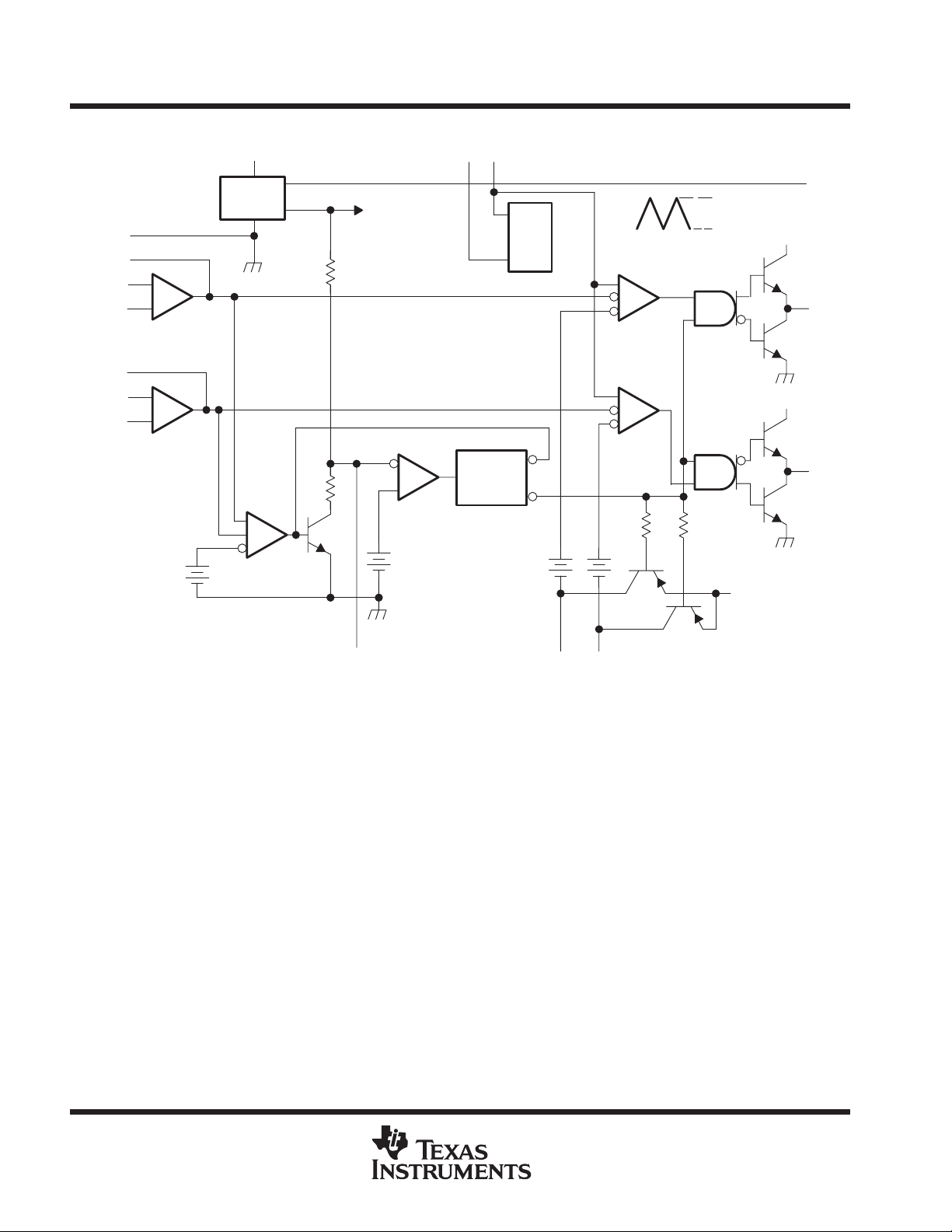
functional block diagram
GND
COMP1
IN1+
IN1–
COMP2
IN2+
IN2–
7
6
4
+
5
_
Error
Amplifier 1
11
13
+
12
_
Error
Amplifier 2
V
CC
10
Voltage
REF
1.25 V
2.5 V
To Internal
Circuitry
SCP
Comparator 2
CTRT
21
UVLO
and
SCP Latch
OSC
PWM
Comparator 1
PWM
Comparator 2
1.8 V
1.2 V
16
REF
V
CC
8
OUT1
V
CC
9
OUT2
1 V
SCP
Comparator 1
SCP
15
1 V
0.65 V
DTC1 DTC2
0.65 V
1.25 V
143
2
POST OFFICE BOX 655303 • DALLAS, TEXAS 75265
POST OFFICE BOX 1443
• HOUSTON, TEXAS 77251–1443
Page 3
TL1454, TL1454Y
DUAL-CHANNEL PULSE-WIDTH-MODULATION (PWM)
CONTROL CIRCUIT
SLVS086B – APRIL 1995 – REVISED NOVEMBER 1997
TL1454Y chip information
This chip, when properly assembled, displays characteristics similar to the TL1454C. Thermal compression or
ultrasonic bonding may be used on the doped aluminum bonding pads. The chips may be mounted with
conductive epoxy or a gold-silicon preform.
BONDING PAD ASSIGNMENTS
(16)
86
(1)
(2) (3)
(12)(13)(14)(15)
(4) (5) (6) (7)
108
(10)(11)
(9)
(8)
CT
RT
DTC1
IN1+
IN1–
COMP1
GND
(1)
(2)
(3)
(4)
(5)
(6)
(7)
(8)
(16)
REF
(15)
SCP
(14)
DTC2
(13)
TL1454Y
POST OFFICE BOX 655303 • DALLAS, TEXAS 75265
POST OFFICE BOX 1443
IN2+
(12)
IN2–
(11)
COMP2
(10)
V
CC
(9)
OUT2OUT1
• HOUSTON, TEXAS 77251–1443
CHIP THICKNESS: 15 TYPICAL
BONDING PADS: 4 × 4 MINIMUM
TJmax = 150°C
TOLERANCES ARE ±10%.
ALL DIMENSIONS ARE IN MILS.
3
Page 4
TL1454, TL1454Y
DUAL-CHANNEL PULSE-WIDTH-MODULATION (PWM)
CONTROL CIRCUIT
SLVS086B – APRIL 1995 – REVISED NOVEMBER 1997
theory of operation
reference voltage
A linear regulator operating from V
generates a 2.5-V supply for the internal circuits and the 1.25-V reference,
CC
which can source a maximum of 1 mA for external loads. A small ceramic capacitor (0.047 µF to 0.1 µF) between
REF and ground is recommended to minimize noise pickup.
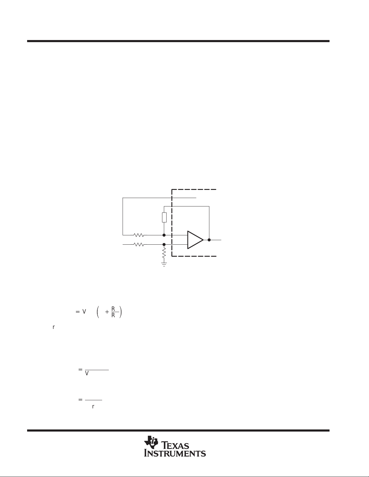
error amplifier
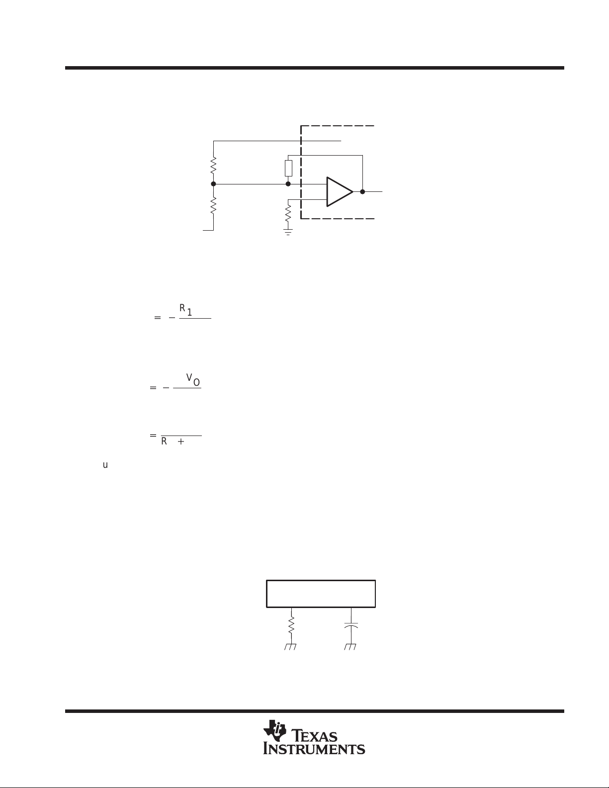
The error amplifier generates the error signal used by the PWM to adjust the power-switch duty cycle for the
desired converter output voltage. The signal is generated by comparing a sample of the output voltage to the
voltage reference and amplifying the difference. An external resistive divider connected between the converter
output and ground, as shown in Figure 1, is generally required to obtain the output voltage sample.
The amplifier output is brought out on COMP to allow the frequency response of the amplifier to be shaped with
an external RC network to stabilize the feedback loop of the converter. DC loading on the COMP output is limited
to 45 µA (the maximum amplifier source current capability).
Figure 1 illustrates the sense-divider network and error-amplifier connections for converters with positive output
voltages. The divider network is connected to the noninverting amplifier input because the PWM has a phase
inversion; the duty cycle decreases as the error-amplifier output increases.
_
+
TL1454
To PWM
Converter
Output
Compensation
V
O
Network
R3
R1
REF
COMP
IN–
IN+
R2
Figure 1. Sense Divider/Error Amplifier
Configuration for Converters with Positive Outputs
The output voltage is given by:
R1
where V
VO+
= 1.25 V.
ref
ǒ
V
1
ref
)
R2
Ǔ
The dc source resistance of the error-amplifier inputs should be 10 kΩ or less and approximately matched to
minimize output voltage errors caused by the input-bias current. A simple procedure for determining appropriate
values for the resistors is to choose a convenient value for R3 (10 kΩ or less) and calculate R1 and R2 using:
R3V
VO–V
R3V
V
ref
O
ref
O
R1+
R2+
4
POST OFFICE BOX 655303 • DALLAS, TEXAS 75265
POST OFFICE BOX 1443
• HOUSTON, TEXAS 77251–1443
Page 5
TL1454, TL1454Y
DUAL-CHANNEL PULSE-WIDTH-MODULATION (PWM)
CONTROL CIRCUIT
SLVS086B – APRIL 1995 – REVISED NOVEMBER 1997
error amplifier
R1 and R2 should be tight-tolerance (±1% or better) devices with low and/or matched temperature coefficients
to minimize output voltage errors. A device with a ±5% tolerance is suitable for R3.
REF
COMP
ref
Compensation
Network
R3
IN–
IN+
_
+
To PWM
R2
R1
Converter
Output
V
O
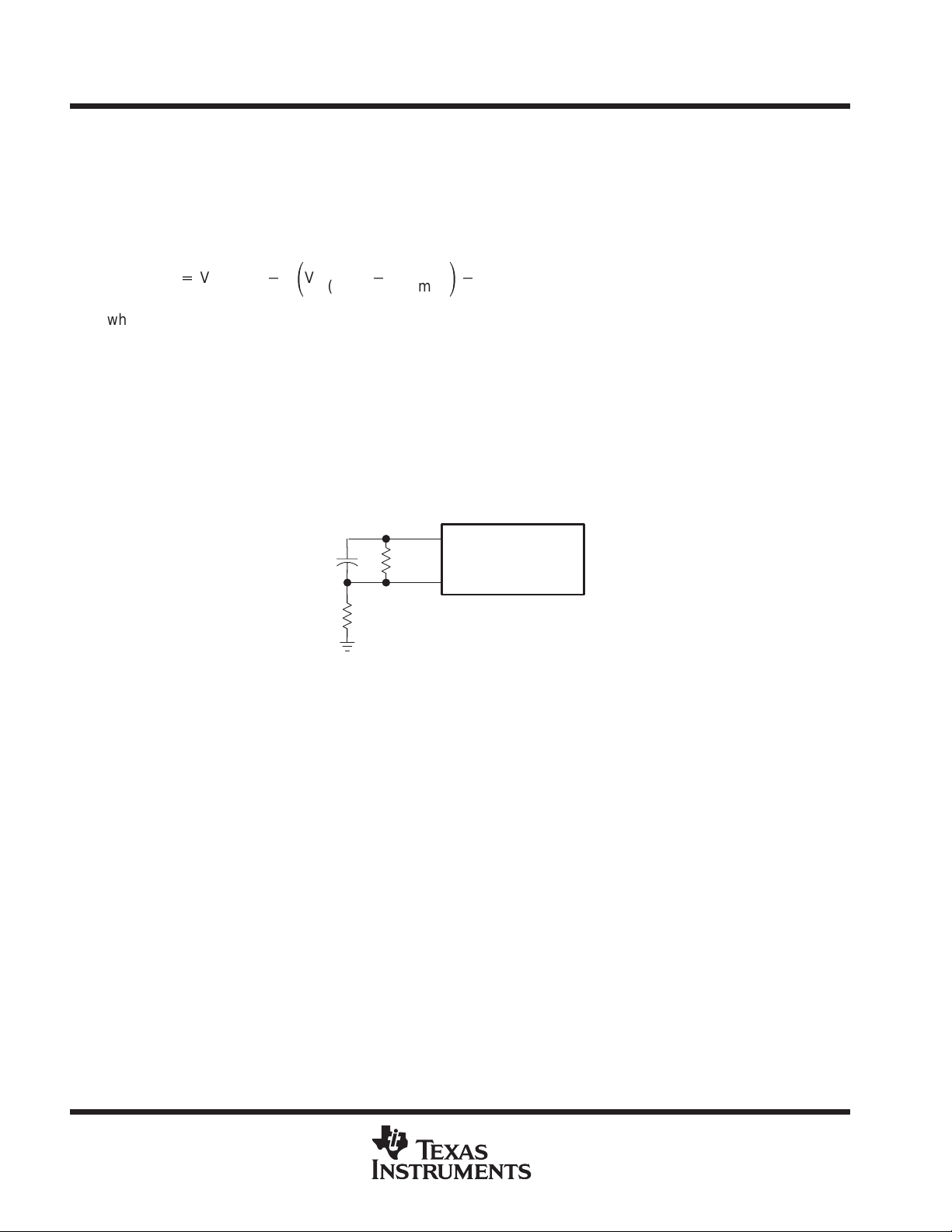
Figure 2. Sense Divider/Error Amplifier Configuration for Converters with Negative Outputs
Figure 2 shows the divider network and error-amplifier configuration for negative output voltages. In general,
the comments for positive output voltages also apply for negative outputs. The output voltage is given by:
R1V
VO+*
R
2
The design procedure for choosing the resistor value is to select a convenient value for R2 (instead of R3 in
the procedure for positive outputs) and calculate R1 and R3 using:
R2V
R1+*
R3+
R1)
V
R1R
ref
O
2
R
2
V alues in the 10-kΩ to 20-kΩ range work well for R2. R3 can be omitted and the noninverting amplifier connected
to ground in applications where the output voltage tolerance is not critical.
oscillator
The oscillator frequency can be set between 50 kHz and 2 MHz with a resistor connected between RT and GND
and a capacitor between CT and GND (see Figure 3). Figure 6 is used to determine R
and CT for the desired
T
operating frequency. Both components should be tight-tolerance, temperature-stable devices to minimize
frequency deviation. A 1% metal-film resistor is recommended for R
capacitor is recommended for C
.
T
TL1454
RT CT
21
R
T
C
T
, and a 10%, or better, NPO ceramic
T
Figure 3. Oscillator Timing
POST OFFICE BOX 655303 • DALLAS, TEXAS 75265
POST OFFICE BOX 1443
• HOUSTON, TEXAS 77251–1443
5
Page 6
TL1454, TL1454Y
DUAL-CHANNEL PULSE-WIDTH-MODULATION (PWM)
CONTROL CIRCUIT
SLVS086B – APRIL 1995 – REVISED NOVEMBER 1997
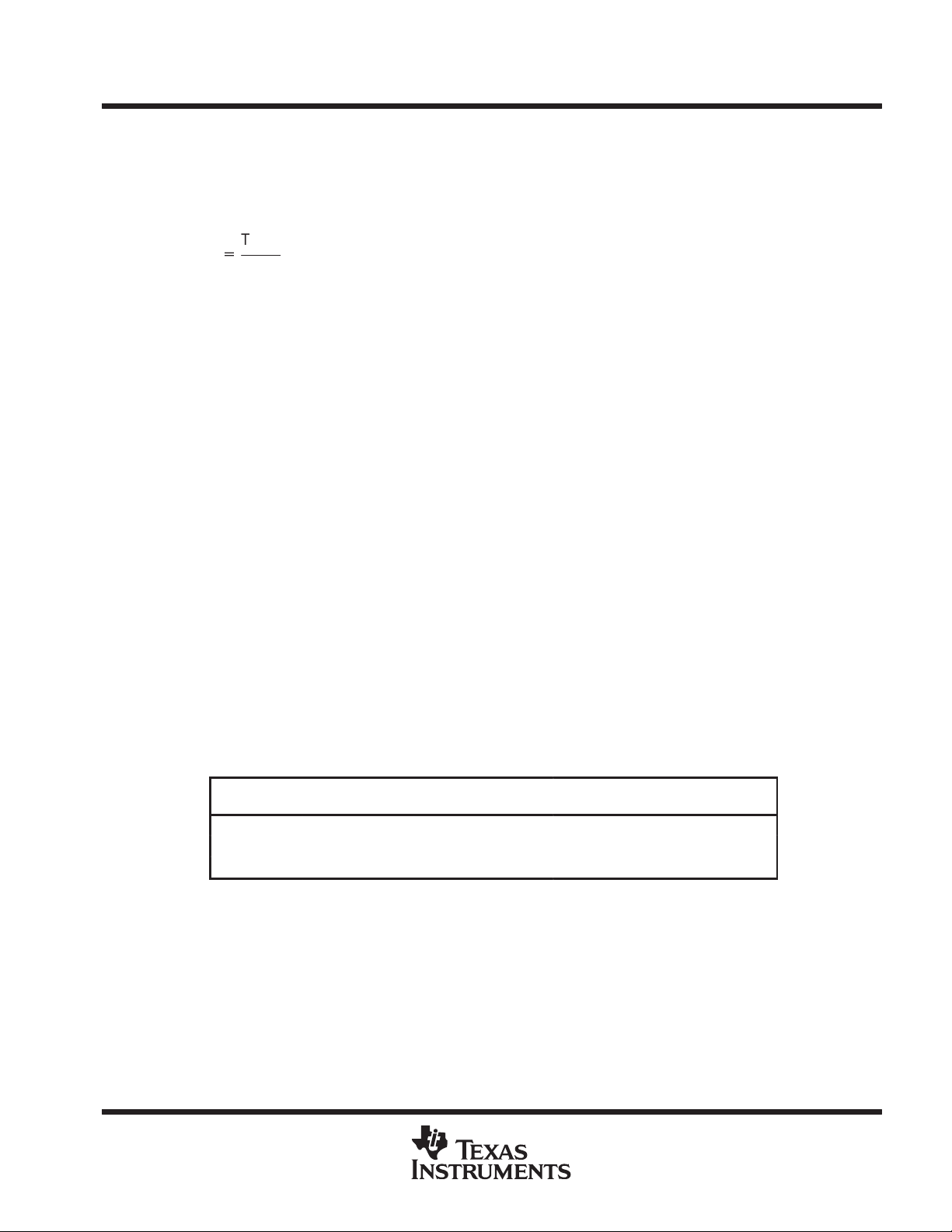
dead-time control (DTC) and soft start
The two PWM channels have independent dead-time control inputs so that the maximum power-switch duty
cycles can be limited to less then 100%. The dead-time is set with a voltage applied to DTC; the voltage is
typically obtained from a resistive divider connected between the reference and ground as shown in Figure 4.
Soft start is implemented by adding a capacitor between REF and DTC.
The voltage, V
VDT+
where V
O(max)
, required to limit the duty cycle to a maximum value is given by:
DT
V
O(max)
and V
ǒ
V
*
D
O(max)
are obtained from Figure 9, and D is the maximum duty cycle.
O(min)
*
V
O(min)
Ǔ
*
0.65
Predicting the regulator startup or rise time is complicated because it depends on many variables, including:
input voltage, output voltage, filter values, converter topology , and operating frequency. In general, the output
will be in regulation within two time constants of the soft-start circuit. A five-to-ten millisecond time constant
usually works well for low-power converters.
The DTC input can be grounded in applications where achieving a 100% duty cycle is desirable, such as a buck
converter with a very low input-to-output differential voltage. However, grounding DTC prevents the
implementation of soft start, and the output voltage overshoot at power-on is likely to be very large. A better
arrangement is to omit R
cycle can reach 100% and still allows the designer to implement soft start using C
(see Figure 4) and choose R
DT1
16
R
DT2
R
DT1
C
SS
REF
DTC
= 47 kΩ. This configuration ensures that the duty
DT2
TL1454
SS
.
Figure 4. Dead-Time Control and Soft Start
PWM comparator
Each of the PWM comparators has dual inverting inputs. One inverting input is connected to the output of the
error amplifier; the other inverting input is connected to the DTC terminal. Under normal operating conditions,
when either the error-amplifier output or the dead-time control voltage is higher than that for the PWM triangle
wave, the output stage is set inactive (OUT1 low and OUT2 high), turning the external power stage off.
undervoltage-lockout (UVLO) protection
The undervoltage-lockout circuit turns the output circuit off and resets the SCP latch whenever the supply
voltage drops too low (to approximately 2.9 V) for proper operation. A hysteresis voltage of 200 mV eliminates
false triggering on noise and chattering.
short-circuit protection (SCP)
The TL1454 SCP function prevents damage to the power switches when the converter output is shorted to
ground. In normal operation, SCP comparator 1 clamps SCP to approximately 185 mV. When one of the
converter outputs is shorted, the error amplifier output (COMP) will be driven below 1 V to maximize duty cycle
and force the converter output back up. When the error amplifier output drops below 1 V, SCP comparator 1
releases SCP, and capacitor, C
error-amplifier output rises above 1 V before C
normal operation resumes. If C
, which is connected between SCP and GND, begins charging. If the
SCP
reaches 1 V , SCP comparator 2 turns on and sets the SCP latch, which turns
SCP
is charged to 1 V , SCP comparator 1 discharges C
SCP
off the output drives and resets the soft-start circuit. The latch remains set until the supply voltage is lowered
to 2 V or less, or C
is discharged externally.
SCP
SCP
and
6
POST OFFICE BOX 655303 • DALLAS, TEXAS 75265
POST OFFICE BOX 1443
• HOUSTON, TEXAS 77251–1443
Page 7
TL1454, TL1454Y
DUAL-CHANNEL PULSE-WIDTH-MODULATION (PWM)
CONTROL CIRCUIT
SLVS086B – APRIL 1995 – REVISED NOVEMBER 1997
short-circuit protection (SCP) (continued)
The SCP time-out period must be greater than the converter start-up time or the converter will not start. Because
high-value capacitor tolerances tend to be ±20% or more and IC resistor tolerances are loose as well, it is best
to choose an SCP time-out period 10-to-15 times greater than the converter startup time. The value of C
may be determined using Figure 6, or it can be calculated using:
T
SCP
+
C
SCP
80.3
SCP
where C
is in µF and T
SCP
is the time-out period in ms.
SCP
output stage
The output stage of the TL1454 is a totem-pole output with a maximum source/sink current rating of 40 mA and
a voltage rating of 20 V . The output is controlled by a complementary output AND gate and is turned on (sourcing
current for OUT1, sinking current for OUT2) when all the following conditions are met: 1) the oscillator triangle
wave voltage is higher than both the DTC voltage and the error-amplifier output voltage, 2) the
undervoltage-lockout circuit is inactive, and 3) the short-circuit protection circuit is inactive.
absolute maximum ratings over operating free-air temperature range (unless otherwise noted)
Supply voltage, V
Error amplifier input voltage: IN1+, IN1–, IN2+, IN2– 23 V. . . . . . . . . . . . . . . . . . . . . . . . . . . . . . . . . . . . . . . . . . .
Output voltage: OUT1, OUT2 20 V. . . . . . . . . . . . . . . . . . . . . . . . . . . . . . . . . . . . . . . . . . . . . . . . . . . . . . . . . . . . . . . .
Continuous output current: OUT1, OUT2 ±200 mA. . . . . . . . . . . . . . . . . . . . . . . . . . . . . . . . . . . . . . . . . . . . . . . . . .
Peak output current: OUT1, OUT2 1 A. . . . . . . . . . . . . . . . . . . . . . . . . . . . . . . . . . . . . . . . . . . . . . . . . . . . . . . . . . . .
Continuous total dissipation See Dissipation Rating Table. . . . . . . . . . . . . . . . . . . . . . . . . . . . . . . . . . . . . . . . . . .
Operating free-air temperature range, T
Storage temperature range, T
Lead temperature 1,6 mm (1/16 inch) from case for 10 seconds 260°C. . . . . . . . . . . . . . . . . . . . . . . . . . . . . . .
†
Stresses beyond those listed under “absolute maximum ratings” may cause permanent damage to the device. These are stress ratings only, and
functional operation of the device at these or any other conditions beyond those indicated under “recommended operating conditions” is not
implied. Exposure to absolute-maximum-rated conditions for extended periods may affect device reliability.
NOTE 1: All voltage values are with respect to network GND.
(see Note 1) 23 V. . . . . . . . . . . . . . . . . . . . . . . . . . . . . . . . . . . . . . . . . . . . . . . . . . . . . . . . . . . .
CC
: C suffix –20°C to 85°C. . . . . . . . . . . . . . . . . . . . . . . . . . . . . . . . . . . .
A
I suffix –40°C to 85°C. . . . . . . . . . . . . . . . . . . . . . . . . . . . . . . . . . . . .
–65°C to 150°C. . . . . . . . . . . . . . . . . . . . . . . . . . . . . . . . . . . . . . . . . . . . . . . . . . .
stg
†
DISSIPATION RATING TABLE
PACKAGE
D 950 mW 7.6 mW/°C 608 mW 494 mW
N 1250 mW 10.0 mW/°C 800 mW 650 mW
PW 500 mW 4.0 mW/°C 320 mW 260 mW
TA ≤ 25°C
POWER RATING
POST OFFICE BOX 655303 • DALLAS, TEXAS 75265
POST OFFICE BOX 1443
DERATING FACTOR
ABOVE TA = 25°C
• HOUSTON, TEXAS 77251–1443
TA = 70°C
POWER RATING
POWER RATING
TA = 85°C
7
Page 8
TL1454, TL1454Y
Operating free-air temperature, T
°C
PARAMETER
TEST CONDITIONS
UNIT
V
Output voltage, REF
V
Output voltage change with temperature
mV
PARAMETER
TEST CONDITIONS
UNIT
PARAMETER
TEST CONDITIONS
UNIT
No pullup
DUAL-CHANNEL PULSE-WIDTH-MODULATION (PWM)
CONTROL CIRCUIT
SLVS086B – APRIL 1995 – REVISED NOVEMBER 1997
recommended operating conditions
MIN MAX UNIT
Supply voltage, V
Error amplifier common-mode input voltage –0.2 1.45 V
Output voltage, V
Output current, I
COMP source current –45 µA
COMP sink current 100 µA
Reference output current 1 mA
COMP dc load resistance 100 kΩ
Timing capacitor , C
Timing resistor , R
Oscillator frequency 50 2000 kHz
p
CC
O
O
T
T
p
A
TL1454C –20 85
TL1454I –40 85
electrical characteristics over recommended operating free-air temperature range, VCC = 6 V,
= 500 kHz (unless otherwise noted)
f
osc
3.6 20 V
20 V
±40 mA
10 4000 pF
5.1 100 kΩ
°
reference
IO = 1 mA, TA = 25°C 1.23 1.25 1.28
IO = 1 mA 1.2 1.31
TA = T
TA = 25°C to 85°C, IO = 1 mA –12.5 –2.5 12.5
= 0 V 30 mA
ref
to 25°C, IO = 1 mA –12.5 –1.25 12.5
A(min)
I
ref
OS
p
Input regulation VOC = 3.6 V to 20 V, IO = 1 mA 2 6 mV
Output regulation IO = 0.1 mA to 1 mA 1 7.5 mV
p
Short-circuit output current V
p
undervoltage lockout (UVLO)
V
IT+
V
IT–
V
hys
Positive-going threshold voltage 2.9 V
Negative-going threshold voltage
Hysteresis, V
IT+
– V
IT–
TA = 25°C
short-circuit protection (SCP)
V
IT
†
V
stby
V
I(latched)
V
IT(COMP)
†
This symbol is not presently listed within EIA/JEDEC standards for semiconductor symbology.
Input threshold voltage TA = 25°C 0.95 1 1.05 V
Standby voltage
Latched-mode input voltage
Comparator threshold voltage COMP1, COMP2 1 V
Input source current TA = 25°C, V
p
p
O(SCP)
TL1454
MIN TYP MAX
TL1454
MIN TYP MAX
2.7 V
100 200 mV
TL1454
MIN TYP MAX
140 185 230 mV
60 120 mV
= 0 –5 –15 –20 µA
8
POST OFFICE BOX 655303 • DALLAS, TEXAS 75265
POST OFFICE BOX 1443
• HOUSTON, TEXAS 77251–1443
Page 9
PARAMETER
TEST CONDITIONS
UNIT
Frequency change with temperature
kH
PARAMETER
TEST CONDITIONS
UNIT
VITInput threshold voltage
V
PARAMETER
TEST CONDITIONS
UNIT
V
PARAMETER
TEST CONDITIONS
UNIT
VOHHigh-level output voltage
V
VOLLow-level output voltage
V
C
2000 pF
T
25°C
ns
TL1454, TL1454Y
DUAL-CHANNEL PULSE-WIDTH-MODULATION (PWM)
CONTROL CIRCUIT
SLVS086B – APRIL 1995 – REVISED NOVEMBER 1997
electrical characteristics over recommended operating free-air temperature range, VCC = 6 V,
= 500 kHz (unless otherwise noted) (continued)
f
osc
oscillator
TL1454
MIN TYP MAX
f
osc
dead-time control (DTC)
V
I(latched)
I
IB
Frequency CT = 120 pF, RT = 10 kΩ 500 kHz
Standard deviation of frequency 50 kHz
Frequency change with voltage VCC = 3.6 V to 20 V, TA = 25°C 5 kHz
p
Maximum ramp voltage 1.8 V
Minimum ramp voltage 1.1 V
p
Latched-mode input voltage 1.2 V
Common-mode input bias current DTC1, IN1+ ≈ 1.2 V 4 µA
Latched-mode (source) current TA = 25°C –100 µA
TA = T
TA = 25°C to 85°C –10 ±20
Duty cycle = 0% 1 1.1 1.2
Duty cycle = 100% 0.4 0.5 0.6
to 25°C –2 ±20
A(min)
MIN TYP MAX
TL1454
z
error-amplifier
TL1454
MIN TYP MAX
V
IO
I
IO
I
IB
V
ICR
A
V
CMRR Common-mode rejection ratio 60 80 dB
V
OM(max)
V
OM(min)
I
O+
I
O–
Input offset voltage 6 mV
Input offset current
Input bias current –160 –500 nA
Input voltage range VCC = 3.6 V to 20 V –0.2 to 1.40 V
Open-loop voltage gain RFB = 200 kΩ 70 80 dB
Unity-gain bandwidth 3 MHz
Positive output voltage swing 2.3 2.43
Negative output voltage swing 0.63 0.8
Output sink current VID = –0.1 V, VO = 1.20 V 0.1 0.5 mA
Output source current VID = 0.1 V, VO = 1.80 V –45 –70 µA
VO = 1.25 V, VIC = 1.25 V
100 nA
output
TL1454
MIN TYP MAX
p
p
t
rv
t
fv
Output voltage rise time
Output voltage fall time
IO = –8 mA VCC–2 4.5
IO = –40 mA VCC–2 4.4
IO = 8 mA 0.1 0.4
IO = 40 mA 1.8 2.5
p
=
L
,
°
=
A
220
220
POST OFFICE BOX 655303 • DALLAS, TEXAS 75265
POST OFFICE BOX 1443
• HOUSTON, TEXAS 77251–1443
9
Page 10

TL1454, TL1454Y
PARAMETER
TEST CONDITIONS
UNIT
PARAMETER
TEST CONDITIONS
UNIT
Output voltage change with temperature
mV
PARAMETER
TEST CONDITIONS
UNIT
PARAMETER
TEST CONDITIONS
UNIT
No pullup
PARAMETER
TEST CONDITIONS
UNIT
Frequency change with temperature
kH
DUAL-CHANNEL PULSE-WIDTH-MODULATION (PWM)
CONTROL CIRCUIT
SLVS086B – APRIL 1995 – REVISED NOVEMBER 1997
electrical characteristics over recommended operating free-air temperature range, VCC = 6 V,
= 500 kHz (unless otherwise noted) (continued)
f
osc
supply current
TL1454
MIN TYP MAX
I
CC(stby)
I
CC(average)
Standby supply current
Average supply current
RT open, CT = 1.5 V, No load,
VO (COMP1, COMP2) = 1.25 V,
RT = 10 kΩ,
50% duty cycle,
CT = 120 pF,
Outputs open
3.1 6 mA
3.5 7 mA
electrical characteristics, VCC = 6 V, f
= 500 kHz, TA = 25°C (unless otherwise noted)
osc
reference
V
I
ref
OS
Output voltage, REF IO = 1 mA, 1.25 V
Input regulation VOC = 3.6 V to 20 V, IO = 1 mA 2 mV
Output regulation IO = 0.1 mA to 1 mA 1 mV
p
Short-circuit output current V
p
IO = 1 mA –1.25
IO = 1 mA –2.5
= 0 V 30 mA
ref
undervoltage lockout (UVLO)
V
IT+
V
IT–
V
hys
Positive-going threshold voltage 2.9 V
Negative-going threshold voltage 2.7 V
Hysteresis, V
IT+
– V
IT–
short-circuit protection (SCP)
V
IT
†
V
stby
V
I(latched)
V
IT(COMP)
†
This symbol is not presently listed within EIA/JEDEC standards for semiconductor symbology.
Input threshold voltage 1 V
Standby voltage
Latched-mode input voltage
Comparator threshold voltage COMP1, COMP2 1 V
Input source current V
p
p
= 0 –15 µA
O(SCP)
TL1454Y
MIN TYP MAX
TL1454Y
MIN TYP MAX
200 mV
TL1454Y
MIN TYP MAX
185 mV
60 mV
oscillator
f
osc
10
Frequency CT = 120 pF, RT = 10 kΩ 500 kHz
Standard deviation of frequency 50 kHz
Frequency change with voltage VCC = 3.6 V to 20 V 5 kHz
Maximum ramp voltage 1.8 V
Minimum ramp voltage 1.1 V
p
POST OFFICE BOX 655303 • DALLAS, TEXAS 75265
POST OFFICE BOX 1443
• HOUSTON, TEXAS 77251–1443
TL1454Y
MIN TYP MAX
–2
–10
z
Page 11
PARAMETER
TEST CONDITIONS
UNIT
VITInput threshold voltage
V
PARAMETER
TEST CONDITIONS
UNIT
V
PARAMETER
TEST CONDITIONS
UNIT
VOHHigh-level output voltage
V
VOLLow-level output voltage
V
C
2000 pF
ns
PARAMETER
TEST CONDITIONS
UNIT
TL1454, TL1454Y
DUAL-CHANNEL PULSE-WIDTH-MODULATION (PWM)
CONTROL CIRCUIT
SLVS086B – APRIL 1995 – REVISED NOVEMBER 1997
electrical characteristics, VCC = 6 V , f
= 500 kHz, TA = 25°C (unless otherwise noted) (continued)
osc
dead-time control (DTC)
TL1454Y
MIN TYP MAX
Duty cycle = 0% 1.1
Duty cycle = 100% 0.5
V
I(latched)
p
Latched-mode input voltage 1.2 V
Latched-mode (source) current –100 µA
error-amplifier
TL1454Y
MIN TYP MAX
I
IB
A
V
CMRR Common-mode rejection ratio 80 dB
V
OM(max)
V
OM(min)
I
O+
I
O–
Input bias current VO = 1.25 V, VIC = 1.25 V –160 nA
Open-loop voltage gain RFB = 200 kΩ 80 dB
Unity-gain bandwidth 3 MHz
Positive output voltage swing 2.43
Negative output voltage swing 0.63
Output sink current VID = –0.1 V, VO = 1.20 V 0.5 mA
Output source current VID = 0.1 V, VO = 1.80 V –70 µA
output
TL1454Y
MIN TYP MAX
p
p
t
rv
t
fv
Output voltage rise time
Output voltage fall time
IO = –8 mA 4.5
IO = –40 mA 4.4
IO = 8 mA 0.1
IO = 40 mA 1.8
p
=
L
220
220
supply current
I
CC(stby)
I
CC(average)
Standby supply current
Average supply current
RT open, CT = 1.5 V, No load,
VO (COMP1, COMP2) = 1.25 V,
RT = 10 kΩ,
50% duty cycle,
POST OFFICE BOX 655303 • DALLAS, TEXAS 75265
POST OFFICE BOX 1443
• HOUSTON, TEXAS 77251–1443
CT = 120 pF,
Outputs open
TL1454Y
MIN TYP MAX
3.1 mA
3.5 mA
11
Page 12

TL1454, TL1454Y
DUAL-CHANNEL PULSE-WIDTH-MODULATION (PWM)
CONTROL CIRCUIT
SLVS086B – APRIL 1995 – REVISED NOVEMBER 1997
PARAMETER MEASUREMENT INFORMATION
Oscillator
COMP
DTC
SCP Reference
OUT1
OUT2
SCP Comparator
Output
SCP
V
CC
2.9-V Typical
Lockout threshold
1.8 V
1.2 V
1 V
H
Dead-Time 100%
L
H
Dead-Time 100%
L
H
L
2.5 V
1 V
0 V
(tpe)
0 V
Figure 5. Timing Diagram
12
POST OFFICE BOX 655303 • DALLAS, TEXAS 75265
POST OFFICE BOX 1443
• HOUSTON, TEXAS 77251–1443
Page 13

TL1454, TL1454Y
DUAL-CHANNEL PULSE-WIDTH-MODULATION (PWM)
CONTROL CIRCUIT
SLVS086B – APRIL 1995 – REVISED NOVEMBER 1997
TYPICAL CHARACTERISTICS
OSCILLATOR FREQUENCY
vs
TIMING RESISTANCE
10 M
100 k
f – Oscillator Frequency – Hz
VCC = 6 V
TA = 25°C
1 M
CT = 300 pF
CT = 1000 pF
10 k
1 k
1 k 10 k 100 k
CT = 3900 pF
RT – Timing Resistance – Ω
CT = 10 pF
CT = 120 pF
Figure 6
OSCILLATOR PERIOD
2
10
VCC = 6 V
RT = 5.1 kΩ
TA = 25°C
sµ
1
10
0
10
t – Oscillation Period –
–1
10
0
10
TIMING CAPACITANCE
1
10
CT – Timing Capacitance – pF
vs
2
10
Figure 7
10
3
10
4
10
5
OSCILLATOR FREQUENCY
vs
FREE-AIR TEMPERATURE
530
VCC = 6 V
RT = 10 kΩ
CT = 120 pF
520
510
500
– Oscillator Frequency – kHz
490
osc
f
480
–50 0 50 100
TA – Free-Air Temperature – ° C
Figure 8
PWM TRIANGLE WAVEFORM AMPLITUDE
2
1.9
1.8
1.7
1.6
1.5
1.4
1.3
1.2
1.1
1
0.9
0.8
VCC = 6 V
0.7
PWM Triangle W aveform Amplitude – V
0.6
0.5
10
RT = 5.1 kΩ
TA = 25°C
0
vs
TIMING CAPACITANCE
V
O(max)
V
O(min)
1
10
Timing Capacitance – pF
10
2
Figure 9
10
3
10
4
POST OFFICE BOX 655303 • DALLAS, TEXAS 75265
POST OFFICE BOX 1443
• HOUSTON, TEXAS 77251–1443
13
Page 14

TL1454, TL1454Y
DUAL-CHANNEL PULSE-WIDTH-MODULATION (PWM)
CONTROL CIRCUIT
SLVS086B – APRIL 1995 – REVISED NOVEMBER 1997
TYPICAL CHARACTERISTICS
1.4
1.2
1
0.8
0.6
DTC Input Threshold Voltage – V
0.4
–50
DTC INPUT THRESHOLD VOLTAGE
vs
FREE-AIR TEMPERATURE
VCC = 6 V
RT = 5.1 kΩ
CT = 1000 pF
VIT (0% Duty Cycle)
VIT (100% Duty Cycle)
0 50 100
TA – Free-Air Temperature – ° C
Figure 10
SCP TIME-OUT PERIOD
SCP CAPACITANCE
2
VCC = 6 V
TA = 25°C
1.5
1
0.5
– SCP Time-Out Period – s
SCP
t
0
0 5 10 15
SCP Capacitance – µF
vs
20 25
Figure 11
1.04
1.02
1
0.98
– SCP Threshold Voltage – V
IT
0.96
V
0.94
–50
SCP THRESHOLD VOLTAGE
vs
FREE-AIR TEMPERATURE
VCC = 6 V
0 50 100
TA – Free-Air Temperature – ° C
Figure 12
3.5
3
2.5
2
– SCP Latch Reset Voltage – V
1.5
I(reset)
V
1
SCP LATCH RESET VOLTAGE
vs
FREE-AIR TEMPERATURE
VCC = 6 V
–25 0 25 50 75 100–50
TA – Free-Air Temperature – ° C
Figure 13
14
POST OFFICE BOX 655303 • DALLAS, TEXAS 75265
POST OFFICE BOX 1443
• HOUSTON, TEXAS 77251–1443
Page 15

TL1454, TL1454Y
DUAL-CHANNEL PULSE-WIDTH-MODULATION (PWM)
CONTROL CIRCUIT
SLVS086B – APRIL 1995 – REVISED NOVEMBER 1997
TYPICAL CHARACTERISTICS
3.5
3
2.5
2
– UVLO Threshold Voltage – V
IT(L)
V
1.5
IT(H)
V
1
–50
UVLO THRESHOLD VOLTAGE
vs
FREE-AIR TEMPERATURE
V
IT(H)
V
IL(L)
–25 0 25 50 75 100
TA – Free-Air Temperature – ° C
Figure 14
120
100
80
60
Duty Cycle – %
40
20
0
0
DUTY CYCLE
DTC INPUT VOLTAGE
0.25
V
I(DTC)
0.5
– DTC Input Voltage – V
Figure 15
vs
0.75
VCC = 6 V
CT = 120 pF
RT = 10 kΩ
TA = 25°C
1.25
1
1.5
ERROR-AMPLIFIER MAXIMUM OUTPUT VOLTAGE
vs
SOURCE CURRENT
2.5
2
1.5
1
0.5
– Error-Amplifier Maximum Output Voltage – V
0
OM +
V
04080
Source Current – µA
VCC = 6 V
VID = 0.1 V
TA = 25°C
Figure 16 Figure 17
120
ERROR-AMPLIFIER MINIMUM OUTPUT VOLTAGE
vs
SINK CURRENT
2.5
VCC = 6 V
VID = 0.1 V
2
1.5
1
0.5
– Error-Amplifier Minimum Output Voltage – V
0
OM –
0 0.5 1 1.5
V
Sink Current – mA
POST OFFICE BOX 655303 • DALLAS, TEXAS 75265
POST OFFICE BOX 1443
• HOUSTON, TEXAS 77251–1443
15
Page 16

TL1454, TL1454Y
DUAL-CHANNEL PULSE-WIDTH-MODULATION (PWM)
CONTROL CIRCUIT
SLVS086B – APRIL 1995 – REVISED NOVEMBER 1997
TYPICAL CHARACTERISTICS
ERROR AMPLIFIER MAXIMUM
PEAK-TO-PEAK OUTPUT VOLTAGE SWING
vs
FREQUENCY
2.5
VCC = 6 V
TA = 25°C
2
1.5
1
Output Voltage Swing – V
0.5
– Error Amplifier Maximum Peak-to-Peak
O(PP)
V
0
1 k 10 k 100 k 1M 10 M 100 M
f – Frequency – Hz
Figure 18
ERROR-AMPLIFIER MINIMUM OUTPUT
0.8
VCC = 6 V
No Load
Amplifier 1
0.7
0.6
0.5
0.4
– Error-Ampplifier Minimum Output Voltage Swing – V
0.3
OM+
V
VOLTAGE SWING
vs
FREE-AIR TEMPERATURE
–25 0 25 50 75 100–50
TA – Free-Air Temperature – ° C
Figure 19
ERROR AMPLIFIER OPEN-LOOP GAIN AND PHASE SHIFT
vs
FREQUENCY
80
VCC = 6 V
TA = 25°C
60
40
Phase Shift
20
0
Error Amplifier Open-Loop Gain – dB
–20
100 1 k 10 k 100 k 1M 10 M
Gain
f – Frequency – Hz
–0°
–36°
–72°
–108°
–144°
–180°
Figure 20
Phase Shift
16
POST OFFICE BOX 655303 • DALLAS, TEXAS 75265
POST OFFICE BOX 1443
• HOUSTON, TEXAS 77251–1443
Page 17

TL1454, TL1454Y
DUAL-CHANNEL PULSE-WIDTH-MODULATION (PWM)
CONTROL CIRCUIT
SLVS086B – APRIL 1995 – REVISED NOVEMBER 1997
TYPICAL CHARACTERISTICS
ERROR-AMPLIFIER POSITIVE OUTPUT
VOLTAGE SWING
vs
FREE-AIR TEMPERATURE
2.5
VCC = 6 V
No Load
Amplifier 1
2.45
2.4
6
5
4
3
– High-Level Output Voltage – V
2
OH
V
– Error-Ampplifier Positive Output Voltage Swing – V
OM+
V
2.35
–25 0 25 50 75 100–50
HIGH-LEVEL OUTPUT VOLTAGE
vs
OUTPUT CURRENT
VCC = 6 V
TA = 25°C
T
– Free-Air Temperature – ° C
Figure 21
5.5
4.5
– High-Level Output Voltage – V
3.5
OH
V
HIGH-LEVEL OUTPUT VOLTAGE
vs
FREE-AIR TEMPERATURE
VCC = 6 V
5
IO = 8 mA
IO = 40 mA
4
1
020406080
I
– Output Current – mA
O
Figure 22
POST OFFICE BOX 655303 • DALLAS, TEXAS 75265
POST OFFICE BOX 1443
• HOUSTON, TEXAS 77251–1443
3
–25 0 25 50 75 100–50
TA – Free-Air Temperature – ° C
Figure 23
17
Page 18

TL1454, TL1454Y
DUAL-CHANNEL PULSE-WIDTH-MODULATION (PWM)
CONTROL CIRCUIT
SLVS086B – APRIL 1995 – REVISED NOVEMBER 1997
TYPICAL CHARACTERISTICS
LOW-LEVEL OUTPUT VOLTAGE
vs
LOW-LEVEL OUTPUT CURRENT
6
VCC = 6 V
TA = 25°C
5
4
3
– Low-Level Output Voltage – V
2
OL
V
1
020406080
I
– Low-Level Output Current – mA
OL
Figure 24
250
VCC = 6 V
IO = 8 mA
200
150
100
– Low-Level Output Voltage – mV
50
OL
V
0
LOW-LEVEL OUTPUT VOLTAGE
vs
FREE-AIR TEMPERATURE
–25 0 25 50 75 100–50
TA – Free-Air Temperature – ° C
Figure 25
3
2.5
2
1.5
– Low-Level Output Voltage – V
1
OL
V
0.5
LOW-LEVEL OUTPUT VOLTAGE
vs
FREE-AIR TEMPERATURE
VCC = 6 V
IO = 40 mA
–25 0 25 50 75 100–50
TA – Free-Air Temperature – ° C
Figure 26
AVERAGE SUPPLY CURRENT
vs
FREE-AIR TEMPERATURE
6
VCC = 6 V
RT = 10 kΩ
CT = 1.5 V
5
COMP1, COMP2 = 1.25 V
No Load
4
3
– Average Supply Current – mA
2
CC(a)
I
1
–50 –25 0 25 50 75
TA – Free-Air Temperature – ° C
Figure 27
100
18
POST OFFICE BOX 655303 • DALLAS, TEXAS 75265
POST OFFICE BOX 1443
• HOUSTON, TEXAS 77251–1443
Page 19
TL1454, TL1454Y
DUAL-CHANNEL PULSE-WIDTH-MODULATION (PWM)
CONTROL CIRCUIT
SLVS086B – APRIL 1995 – REVISED NOVEMBER 1997
TYPICAL CHARACTERISTICS
STANDBY SUPPLY CURRENT
vs
SUPPLY VOLTAGE
6
VCC = 6 V
RT = Open
CT = 1.5 V
5
COMP1, COMP2 = 1.25 V
No Load
TA = 25°C
4
3
– Standby Supply Current – mA
2
CC(stby)
I
1
0 5 10 15 20 25
VCC – Supply Voltage – V
Figure 28
STANDBY SUPPLY CURRENT
FREE-AIR TEMPERATURE
6
VCC = 6 V
CT = 1.5 V
RT = Open
5
COMP1, COMP2 = 1.25 V
No Load
4
3
– Standby Supply Current – mA
2
CC(stby)
I
1
– 50 0 50
TA – Free-Air Temperature – ° C
Figure 29
vs
100
REFERENCE VOLTAGE
vs
SUPPLY VOLTAGE
1.5
TA = 25°C
1
0.5
– Reference Voltage – V
ref
V
0
0 5 10 15 20 25
VCC – Supply Voltage – V
Figure 30
REFERENCE VOLTAGE
vs
SUPPLY VOLTAGE
1.26
IO = 1mA
TA = 25°C
1.25
1.24
– Reference Voltage – V
ref
V
1.23
0 5 10 15 20 25
VCC – Supply Voltage – V
Figure 31
POST OFFICE BOX 655303 • DALLAS, TEXAS 75265
POST OFFICE BOX 1443
• HOUSTON, TEXAS 77251–1443
19
Page 20
TL1454, TL1454Y
DUAL-CHANNEL PULSE-WIDTH-MODULATION (PWM)
CONTROL CIRCUIT
SLVS086B – APRIL 1995 – REVISED NOVEMBER 1997
TYPICAL CHARACTERISTICS
REFERENCE VOLTAGE
vs
FREE-AIR TEMPERATURE
1.26
VCC = 6 V
IO = –1 mA
1.25
– Reference Voltage – V
1.24
ref
V
1.23
–50
–25 0 25 50 75 100
TA – Free-Air Temperature – ° C
Figure 32
20
POST OFFICE BOX 655303 • DALLAS, TEXAS 75265
POST OFFICE BOX 1443
• HOUSTON, TEXAS 77251–1443
Page 21

TL1454, TL1454Y
DUAL-CHANNEL PULSE-WIDTH-MODULATION (PWM)
CONTROL CIRCUIT
SLVS086B – APRIL 1995 – REVISED NOVEMBER 1997
MECHANICAL DATA
D (R-PDSO-G**) PLASTIC SMALL-OUTLINE PACKAGE
14 PIN SHOWN
14
1
0.069 (1,75) MAX
0.050 (1,27)
A
0.020 (0,51)
0.014 (0,35)
0.010 (0,25)
0.004 (0,10)
8
7
0.010 (0,25)
0.157 (4,00)
0.150 (3,81)
M
0.244 (6,20)
0.228 (5,80)
Seating Plane
0.004 (0,10)
PINS **
DIM
A MAX
A MIN
0.008 (0,20) NOM
Gage Plane
0°–8°
8
0.197
(5,00)
0.189
(4,80)
14
0.344
(8,75)
0.337
(8,55)
0.010 (0,25)
0.044 (1,12)
0.016 (0,40)
4040047/B 10/94
16
0.394
(10,00)
0.386
(9,80)
NOTES: A. All linear dimensions are in inches (millimeters).
B. This drawing is subject to change without notice.
C. Body dimensions do not include mold flash or protrusion not to exceed 0.006 (0,15).
D. Four center pins are connected to die mount pad
E. Falls within JEDEC MS-012
POST OFFICE BOX 655303 • DALLAS, TEXAS 75265
POST OFFICE BOX 1443
• HOUSTON, TEXAS 77251–1443
21
Page 22

TL1454, TL1454Y
DUAL-CHANNEL PULSE-WIDTH-MODULATION (PWM)
CONTROL CIRCUIT
SLVS086B – APRIL 1995 – REVISED NOVEMBER 1997
MECHANICAL DATA
N (R-PDIP-T**) PLASTIC DUAL-IN-LINE P ACKAGE
16 PIN SHOWN
A
16
9
PINS **
DIM
14
16
18
20
1
0.035 (0,89) MAX
0.021 (0,53)
0.015 (0,38)
0.070 (1,78) MAX
0.020 (0,51) MIN
0.100 (2,54)
0.010 (0,25)
A MAX
0.260 (6,60)
0.240 (6,10)
8
0.200 (5,08) MAX
0.125 (3,18) MIN
M
0.010 (0,25) NOM
A MIN
Seating Plane
0.775
(19,69)
0.745
(18,92)
0.775
(19,69)
0.745
(18,92)
0.920
(23.37)
0.850
(21.59)
0.975
(24,77)
0.940
(23,88)
0.310 (7,87)
0.290 (7,37)
0°–15°
NOTES: A. All linear dimensions are in inches (millimeters).
22
B. This drawing is subject to change without notice.
C. Falls within JEDEC MS-001 (20-pin package is shorter than MS-001)
POST OFFICE BOX 655303 • DALLAS, TEXAS 75265
POST OFFICE BOX 1443
14 Pin Only
4040049/C 7/95
• HOUSTON, TEXAS 77251–1443
Page 23

TL1454, TL1454Y
DUAL-CHANNEL PULSE-WIDTH-MODULATION (PWM)
CONTROL CIRCUIT
SLVS086B – APRIL 1995 – REVISED NOVEMBER 1997
MECHANICAL DATA
PW (R-PDSO-G**) PLASTIC SMALL-OUTLINE PACKAGE
14 PIN SHOWN
0,65
14
1
1,20 MAX
A
7
0,10 MIN
0,32
0,17
8
6,70
4,70
4,30
6,10
M
0,13
Seating Plane
0,10
0,15 NOM
Gage Plane
0,25
0°–8°
0,70
0,40
PINS **
DIM
A MAX
A MIN
NOTES: A. All linear dimensions are in millimeters.
B. This drawing is subject to change without notice.
C. Body dimensions do not include mold flash or protrusion not to exceed 0,15.
8
3,30
2,90
14
5,30
4,90
16
5,30
20
6,80
6,404,90
24
8,10
7,70
28
10,00
9,60
4040064/B 10/94
POST OFFICE BOX 655303 • DALLAS, TEXAS 75265
POST OFFICE BOX 1443
• HOUSTON, TEXAS 77251–1443
23
Page 24

IMPORTANT NOTICE
T exas Instruments and its subsidiaries (TI) reserve the right to make changes to their products or to discontinue
any product or service without notice, and advise customers to obtain the latest version of relevant information
to verify, before placing orders, that information being relied on is current and complete. All products are sold
subject to the terms and conditions of sale supplied at the time of order acknowledgement, including those
pertaining to warranty, patent infringement, and limitation of liability.
TI warrants performance of its semiconductor products to the specifications applicable at the time of sale in
accordance with TI’s standard warranty. Testing and other quality control techniques are utilized to the extent
TI deems necessary to support this warranty . Specific testing of all parameters of each device is not necessarily
performed, except those mandated by government requirements.
CERT AIN APPLICATIONS USING SEMICONDUCTOR PRODUCTS MAY INVOLVE POTENTIAL RISKS OF
DEATH, PERSONAL INJURY, OR SEVERE PROPERTY OR ENVIRONMENTAL DAMAGE (“CRITICAL
APPLICATIONS”). TI SEMICONDUCTOR PRODUCTS ARE NOT DESIGNED, AUTHORIZED, OR
WARRANTED TO BE SUITABLE FOR USE IN LIFE-SUPPORT DEVICES OR SYSTEMS OR OTHER
CRITICAL APPLICA TIONS. INCLUSION OF TI PRODUCTS IN SUCH APPLICATIONS IS UNDERST OOD TO
BE FULLY AT THE CUSTOMER’S RISK.
In order to minimize risks associated with the customer’s applications, adequate design and operating
safeguards must be provided by the customer to minimize inherent or procedural hazards.
TI assumes no liability for applications assistance or customer product design. TI does not warrant or represent
that any license, either express or implied, is granted under any patent right, copyright, mask work right, or other
intellectual property right of TI covering or relating to any combination, machine, or process in which such
semiconductor products or services might be or are used. TI’s publication of information regarding any third
party’s products or services does not constitute TI’s approval, warranty or endorsement thereof.
Copyright 1998, Texas Instruments Incorporated
 Loading...