

(MHz)
(V/µs)
GAIN
PHASE
(nV/√Hz)
查询THS3001供应商
THS3001, THS3002
420-MHz HIGH-SPEED CURRENT-FEEDBACK AMPLIFIERS
SLOS217A – JULY 1998 – REVISED JUNE 1999
D
High Speed
– 420 MHz Bandwidth (G = 1, –3 dB)
– 6500 V/µs Slew Rate
– 40-ns Settling Time (0.1%)
D
High Output Drive, IO = 100 mA
D
Excellent Video Performance
– 115 MHz Bandwidth (0.1 dB, G = 2)
– 0.01% Differential Gain
– 0.02° Differential Phase
D
Low 3-mV (max) Input Offset Voltage
D
Very Low Distortion
– THD = –96 dBc at f = 1 MHz
– THD = –80 dBc at f = 10 MHz
D
Wide Range of Power Supplies
– V
D
Evaluation Module Available
= ±4.5 V to ±16 V
CC
description
The THS300x is a high-speed current-feedback
operational amplifier, ideal for communication,
imaging, and high-quality video applications. This
device offers a very fast 6500-V/µs slew rate, a
420-MHz bandwidth, and 40-ns settling time for
large-signal applications requiring excellent transient response. In addition, the THS300x
operates with a very low distortion of – 96 dBc,
making it well suited for applications such as
wireless communication basestations or ultrafast
ADC or DAC buffers.
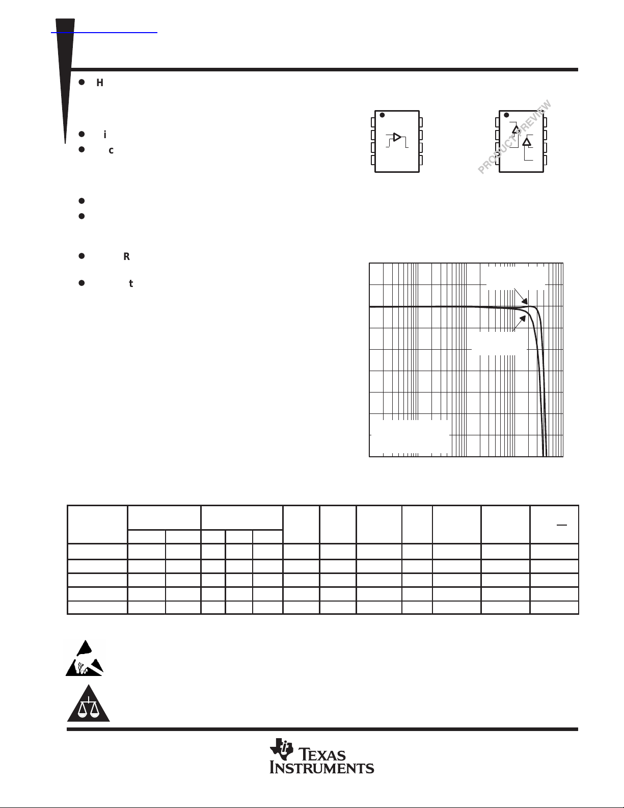
THS3001
D AND DGN† PACKAGE
(TOP VIEW)
NULL
V
NC – No internal connection
†
1
IN–
2
IN+
3
4
CC–
The THS3001 implemented in the DGN package is in the
product preview stage of development. Contact your local TI
sales office for availability.
NULL
8
V
7
CC+
OUT
6
5
NC
1OUT
–V
THS3002
D AND DGN PACKAGE
(TOP VIEW)
1IN–
1IN+
CC
1
2
3
4
8
7
6
5
OUTPUT AMPLITUDE
vs
FREQUENCY
8
7
6
5
4
3
2
Output Amplitude – dB
1
G = 2
0
RL = 150 Ω
VI = 200 mV RMS
–1
1M 100M
10M 1G100k
f – Frequency – Hz
VCC = ±15 V
RF = 680 Ω
VCC = ±5 V
RF = 750 Ω
V
CC+
2OUT
2IN–
2IN+
HIGH-SPEED AMPLIFIER FAMILY
DEVICE
THS3001/02 • • • 420 6500 –96 40 0.01% 0.02° 1.6
THS4001 • • • • 270 400 –72 40 0.04% 0.15° 12.5
THS4011/12 • • • 290 310 –80 37 0.006% 0.01° 7.5
THS4031/32 • • • 100 100 –72 60 0.02% 0.03° 1.6
THS4061/62 • • • 180 400 –72 40 0.02% 0.02° 14.5
PRODUCTION DATA information is current as of publication date.
Products conform to specifications per the terms of Texas Instruments
standard warranty. Production processing does not necessarily include
testing of all parameters.
ARCHITECTURE
VFB CFB 5 V ±5 V ±15 V
CAUTION: The THS300x provides ESD protection circuitry. However, permanent damage can still occur if this device is subjected
to high-energy electrostatic discharges. Proper ESD precautions are recommended to avoid any performance degradation or loss
of functionality.
Please be aware that an important notice concerning availability, standard warranty, and use in critical applications of
Texas Instruments semiconductor products and disclaimers thereto appears at the end of this data sheet.
SUPPLY
VOLTAGE
POST OFFICE BOX 655303 • DALLAS, TEXAS 75265
BW
SR
THD
f = 1 MHz
(dB) (ns)
t
s
0.1%
DIFF.
Copyright 1999, Texas Instruments Incorporated
DIFF.
V
n
1
THS3001, THS3002
†
MODULE
PACKAGE
A
A
A
Suppl
oltage, V
and V
V
Operating free-air temperature, T
°C
420-MHz HIGH-SPEED CURRENT-FEEDBACK AMPLIFIERS
SLOS217A – JULY 1998 – REVISED JUNE 1999
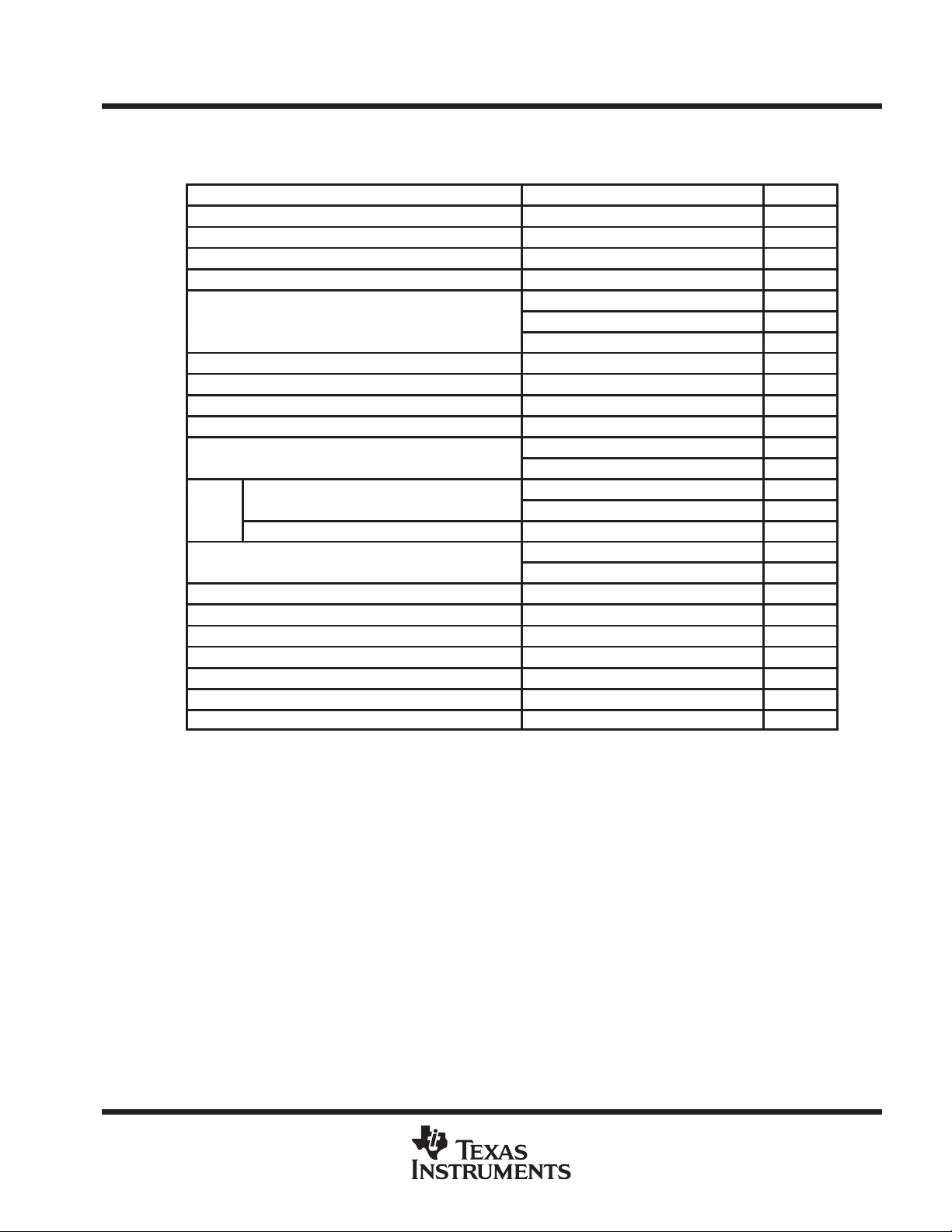
AVAILABLE OPTIONS
PACKAGED DEVICE
T
A
0°C to 70°C
–40°C to 85°C
†
The D package is available taped and reeled. Add an R suffix to the device type (i.e.,
THS3001CDR)
‡
Product Preview
SOIC
(D)
THS3001CD
THS3002CD
THS3001ID
THS3002ID
THS3001CDGN
‡
THS3002CDGN
THS3001IDGN
‡
THS3002IDGN
MSOP (DGN)
DEVICE SYMBOL
‡
TIADP
‡
‡
TIADQ
‡
TIADI
TIADJ
EVALUATION
THS3001EVM
THS3002EVM
—
‡
absolute maximum ratings over operating free-air temperature range (unless otherwise noted)
Supply voltage, V
Input voltage, V
Output Current, I
to V
CC+
±V
. . . . . . . . . . . . . . . . . . . . . . . . . . . . . . . . . . . . . . . . . . . . . . . . . . . . . . . . . . . . . . . . . . . . . . . . . .
I
175 mA. . . . . . . . . . . . . . . . . . . . . . . . . . . . . . . . . . . . . . . . . . . . . . . . . . . . . . . . . . . . . . . . . . . . . .
O
Differential input voltage, V
Continuous total power dissipation See Dissipation Rating Table. . . . . . . . . . . . . . . . . . . . . . . . . . . . . . . . . . . . .
Operating free-air temperature, T
Storage temperature, T
stg
Lead temperature, 1,6 mm (1/16 inch) from case for 10 seconds 300°C. . . . . . . . . . . . . . . . . . . . . . . . . . . . . . .
†
Stresses beyond those listed under “absolute maximum ratings” may cause permanent damage to the device. These are stress ratings only, and
functional operation of the device at these or any other conditions beyond those indicated under “recommended operating conditions” is not
implied. Exposure to absolute-maximum-rated conditions for extended periods may affect device reliability.
POWER RATING ABOVE TA = 25°C
D 740 mW 6 mW/°C 470 mW 380 mW
33 V. . . . . . . . . . . . . . . . . . . . . . . . . . . . . . . . . . . . . . . . . . . . . . . . . . . . . . . . . . . . . . .
CC–
±6 V. . . . . . . . . . . . . . . . . . . . . . . . . . . . . . . . . . . . . . . . . . . . . . . . . . . . . . . . . . . . . . . .
ID
, THS300xC 0°C to 70°C. . . . . . . . . . . . . . . . . . . . . . . . . . . . . . . . . . . . . . . .
A
THS300xI –40°C to 85°C. . . . . . . . . . . . . . . . . . . . . . . . . . . . . . . . . . . . . . .
–65°C to 125°C. . . . . . . . . . . . . . . . . . . . . . . . . . . . . . . . . . . . . . . . . . . . . . . . . . . . . . . .
DISSIPATION RATING TABLE
T
≤ 25°C DERATING FACTOR T
= 70°C T
POWER RATING
= 85°C
POWER RATING
recommended operating conditions
MIN NOM MAX UNIT
pp
y v
p
CC+
CC–
p
A
Split supply ±4.5 ±16
Single supply 9 32
THS300xC 0 70
THS300xI –40 85
°
†
CC
2
POST OFFICE BOX 655303 • DALLAS, TEXAS 75265
VCCPower supply operating range
V
V
V
ICCQuiescent current
mA
V
±15 V
V
±5 V
VOOutput voltage swing
V
V
±15 V
IOOutput current (see Note 1)
mA
VIOInput offset voltage
V
±15 V
mV
In ut
IIBIn ut bias current
V
CC
±15 V
µA
Input
V
Common-mode input voltage range
V
Oen loo transresistance
MΩ
CMRR
Common-mode rejection ratio
dB
V
±5 V
dB
PSRR
Power supply rejection ratio
V
±15 V
dB
RIInput resistance
InInput current noise
CC
,
,
A/√H
THS3001, THS3002
420-MHz HIGH-SPEED CURRENT-FEEDBACK AMPLIFIERS
SLOS217A – JULY 1998 – REVISED JUNE 1999
electrical characteristics, TA = 25°C, RL = 150 Ω, RF = 1 kΩ (unless otherwise noted)
PARAMETER TEST CONDITIONS
pp
p
p
p
p
Input offset voltage drift VCC = ±5 V or ±15 V 5 µV/°C
p
–
p
p
+
ICR
p
p
pp
p
C
I
R
O
V
n
†
Full range = 0°C to 70°C for the THS300xC and –40°C to 85°C for the THS300xI.
NOTE 1: Observe power dissipation ratings to keep the junction temperature below absolute maximum when the output is heavily loaded or
Differential input capacitance 7.5 pF
Output resistance Open loop at 5 MHz 10 Ω
Input voltage noise
p
shorted. See absolute maximum ratings section.
p
+Input 1.5 MΩ
–Input 15 Ω
Positive (IN+)
Negative (IN–)
Split supply ±4.5 ±16.5
Single supply 9 33
= ±5
CC
=
CC
=
CC
=
CC
VCC = ±5 V, RL = 20 Ω 100
VCC = ±15 V, RL = 75 Ω 85 120
= ±5 V or
CC
= ±5 V or
VCC = ±5 V ±3 ±3.2
VCC = ±15 V ±12.9 ±13.2
VCC = ±5 V,
RL = 1 kΩ
VCC = ±15 V,
RL = 1 kΩ
VCC = ±5 V, VCM = ±2.5 V 62 70
VCC = ±15 V, VCM = ±10 V 65 73
=
CC
=
CC
VCC = ±5 V or ±15 V, f = 10 kHz,
G = 2
V
= ±5 V or ±15 V, f = 10 kHz,
G = 2
†
TA = 25°C 5.5 7.5
TA = full range 8.5
TA = 25°C 6.6 9
TA = full range 10
RL = 150 Ω ±2.9 ±3.2
RL = 1 kΩ ±3 ±3.3
RL = 150 Ω ±12.1 ±12.8
RL = 1 kΩ ±12.8 ±13.1
TA = 25°C 1 3
TA = full range 4
TA = 25°C 2 10
TA = full range 15
TA = 25°C 1 10
TA = full range 15
VO = ±2.5 V ,
VO = ±7.5 V ,
TA = 25°C 65 76
TA = full range 63
TA = 25°C 69 76
TA = full range 67
MIN TYP MAX UNIT
1.3
2.4
1.6 nV/√Hz
13
16
p
z
POST OFFICE BOX 655303 • DALLAS, TEXAS 75265
3
THS3001, THS3002
CC
,
SR
Slew rate (see Note 2)
V/µs
CC
,
t
ns
ADDifferential gain error
,
θDDifferential phase error
,
G
R
Bandwidth for 0.1 dB flatness
MH
V
O(PP)
Full ower bandwidth (see Note 3)
V
O(PP)
V
420-MHz HIGH-SPEED CURRENT-FEEDBACK AMPLIFIERS
SLOS217A – JULY 1998 – REVISED JUNE 1999
operating characteristics, TA = 25°C, RL = 150 Ω, RF = 1 kΩ (unless otherwise noted)
PARAMETER TEST CONDITIONS MIN TYP MAX UNIT
V
= ±5 V,
V
= 4 V
O(PP)
V
= ±15 V,
V
= 20 V
O(PP)
Settling time to 0.1%
s
Settling time to 0.1%
THD Total harmonic distortion
p
Small signal bandwidth (–3 dB)
BW
p
Crosstalk (THS3002 only) TBD dB
NOTES: 2. Slew rate is measured from an output level range of 25% to 75%.
3. Full power bandwidth is defined as the frequency at which the output has 3% THD.
VCC = ±15 V,
0 V to 10 V Step
VCC = ±5 V,
0 V to 2 V Step,
VCC = ±15 V,
fc = 10 MHz,
G = 2,
40 IRE modulation,
±100 IRE Ramp,
NTSC and PAL
G = 2,
40 IRE modulation,
±100 IRE Ramp,
NTSC and PAL
= 1,
G = 2, RF = 750 Ω, VCC = ±5 V 300
G = 2, RF = 680 Ω, VCC = ±15 V 385
G = 5, RF = 560 Ω, VCC = ±15 V 350
G = 2, RF = 750 Ω, VCC = ±5 V 85
G = 2, RF = 680 Ω, VCC = ±15 V 115
VCC = ±5 V,
RL = 500 Ω
VCC = ±15 V,
RL = 500 Ω
= 1 kΩ,
F
= 4 V,
= 20
G = –5 1700
G = 5 1300
G = –5 6500
G = 5 6300
Gain = –1,
Gain = –1,
V
= 2 V,
O(PP)
G = 2
VCC = ±5 V 0.015%
VCC = ±15 V 0.01%
VCC = ±5 V 0.01°
VCC = ±15 V 0.02°
VCC = ±5 V, 330 MHz
VCC = ±15 V, 420 MHz
G = –5 65 MHz
G = 5 62 MHz
G = –5 32 MHz
G = 5 31 MHz
40
25
–80 dBc
MHz
z
4
PARAMETER MEASUREMENT INFORMATION
R
G
V
I
50 Ω
Figure 1. Test Circuit, Gain = 1 + (RF/RG)
POST OFFICE BOX 655303 • DALLAS, TEXAS 75265
R
F
VCC+
–
+
VCC–
V
O
R
L
PSRR
Power supply rejection ratio
Slew rate
Harmonic distortion
THS3001, THS3002
420-MHz HIGH-SPEED CURRENT-FEEDBACK AMPLIFIERS
SLOS217A – JULY 1998 – REVISED JUNE 1999
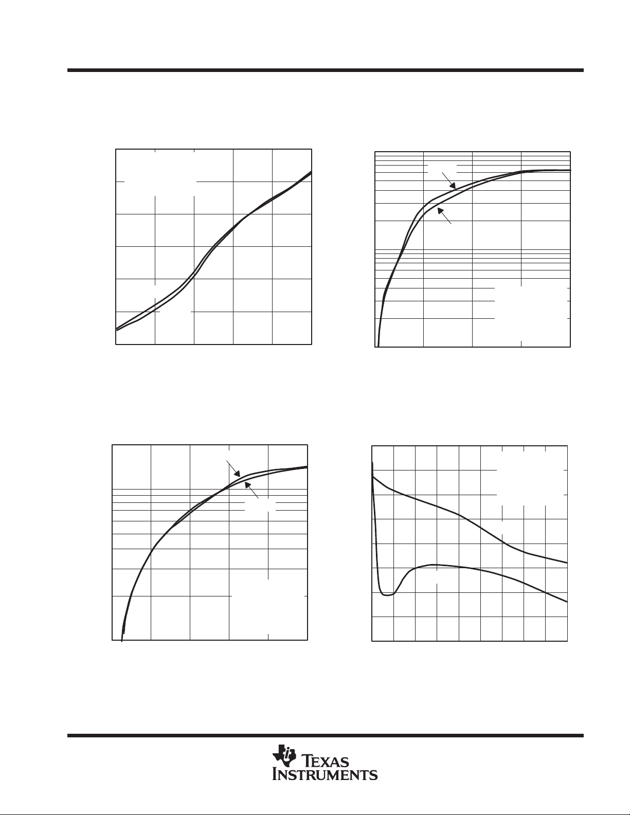
TYPICAL CHARACTERISTICS
Table of Graphs
FIGURE
|VO| Output voltage swing vs Free-air temperature 2
I
CC
I
IB
V
IO
CMRR Common-mode rejection ratio
V
n
I
n
SR
Current supply vs Free-air temperature 3
Input bias current vs Free-air temperature 4
Input offset voltage vs Free-air temperature 5
vs Common-mode input voltage 6
vs Common-mode input voltage 7
vs Frequency 8
Transresistance vs Free-air temperature 9
Closed-loop output impedance vs Frequency 10
Voltage noise vs Frequency 11
Current noise vs Frequency 11
pp
Normalized slew rate vs Gain 17
Differential gain vs Loading 22, 23
Differential phase vs Loading 24, 25
Output amplitude vs Frequency 26–30
Normalized output response vs Frequency 31–34
Small and large signal frequency response 35, 36
Small signal pulse response 37, 38
Large signal pulse response 39 – 46
vs Frequency 12
vs Free-air temperature 13
vs Supply voltage 14
vs Output step peak-to-peak 15, 16
vs Peak-to-peak output voltage swing 18, 19
vs Frequency 20, 21
POST OFFICE BOX 655303 • DALLAS, TEXAS 75265
5
THS3001, THS3002
420-MHz HIGH-SPEED CURRENT-FEEDBACK AMPLIFIERS
SLOS217A – JULY 1998 – REVISED JUNE 1999
TYPICAL CHARACTERISTICS
OUTPUT VOLTAGE SWING
vs
FREE-AIR TEMPERATURE
14
13
12
4
3.5
3
2.5
2
VCC = ±15 V
No Load
VCC = ±5 V
No Load
–20 20
0 40 100–40
TA – Free-Air Temperature – ° C
VCC = ±15 V
RL = 150 Ω
VCC = ±5 V
RL = 150 Ω
60 80
13.5
12.5
– Output Voltage Swing – VV
O
9
8
7
6
5
– Supply Current – mA
CC
I
4
3
–20 20
Figure 2
INPUT BIAS CURRENT
vs
FREE-AIR TEMPERATURE
–0.5
0
CURRENT SUPPLY
vs
FREE-AIR TEMPERATURE
VCC = ±15 V
VCC = ±10 V
VCC = ±5 V
0 40 100–40
TA – Free-Air Temperature – ° C
60 80
Figure 3
INPUT OFFSET VOLTAGE
vs
FREE-AIR TEMPERATURE
–1
Aµ
–1.5
–2
– Input Bias Current –
IB
I
–2.5
–3
–40 –20 0 20 80 100
TA – Free-Air Temperature – ° C
VCC = ±5 V
VCC = ±15 V
VCC = ±5 V
VCC = ±15 V
6040
Figure 4
I
IB+
I
I
I
IB+
IB–
IB–
–0.2
–0.4
–0.6
–0.8
– Input Offset Voltage – mV
IO
V
–1
–1.2
Gain = 1
RF = 1 kΩ
–20 20
0 40 100–40
TA – Free-Air Temperature – ° C
Figure 5
VCC = ±5 V
VCC = ±15 V
60 80
6
POST OFFICE BOX 655303 • DALLAS, TEXAS 75265
THS3001, THS3002
420-MHz HIGH-SPEED CURRENT-FEEDBACK AMPLIFIERS
SLOS217A – JULY 1998 – REVISED JUNE 1999
TYPICAL CHARACTERISTICS
COMMON-MODE REJECTION RATIO
vs
COMMON-MODE INPUT VOLTAGE
80
TA = –40°C
70
TA = 85°C
TA = 25°C
60
50
40
CMRR – Common-Mode Rejection Ratio – dB
VCC = ±15 V
30
2648 14
0
|VIC| – Common-Mode Input Voltage – V
Figure 6
COMMON-MODE REJECTION RATIO
vs
FREQUENCY
80
VCC = ±15 V
70
VCC = ±5 V
60
50
40
30
20
V
I
10
CMRR – Common-Mode Rejection Ratio – dB
0
1k 10k 10M 100M1M100k
1 kΩ
1 kΩ
–
+
1 kΩ
1 kΩ
f – Frequency – Hz
V
O
Figure 8
10 12
COMMON-MODE REJECTION RATIO
vs
COMMON-MODE INPUT VOLTAGE
80
TA = –40°C
70
TA = 85°C
60
50
40
30
CMRR – Common-Mode Rejection Ratio – dB
VCC = ±5 V
20
0.5 1.512 4
0
|VIC| – Common-Mode Input Voltage – V
TA = 25°C
2.5 3
Figure 7
TRANSRESISTANCE
vs
FREE-AIR TEMPERATURE
2.8
2.6
2.4
2.2
2
1.8
1.6
Transresistance – MΩ
1.4
1.2
VO = VCC/2
RL = 1 kΩ
1
–40
–20 20
0 40 100
TA – Free-Air Temperature – ° C
VCC = ±15 V
VCC = ±10 V
VCC = ±5 V
Figure 9
3.5
60 80
POST OFFICE BOX 655303 • DALLAS, TEXAS 75265
7
THS3001, THS3002
420-MHz HIGH-SPEED CURRENT-FEEDBACK AMPLIFIERS
SLOS217A – JULY 1998 – REVISED JUNE 1999
TYPICAL CHARACTERISTICS
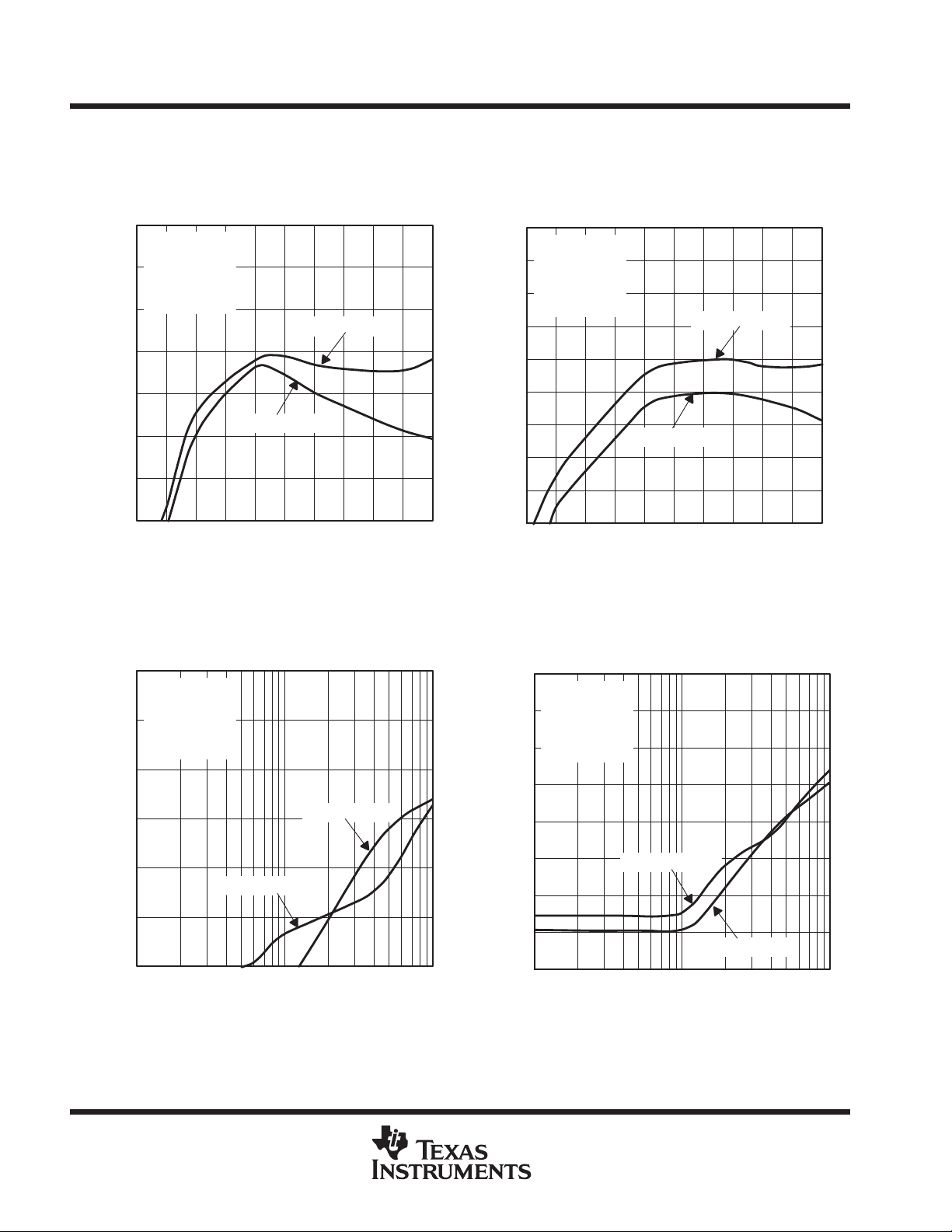
CLOSED-LOOP OUTPUT IMPEDANCE
vs
FREQUENCY
100
VCC = ±15 V
RF = 750 Ω
Ω
Closed-Loop Output Impedance –
Gain = +2
TA = 25°C
10
V
= 2 V
I(PP)
1
750 Ω
0.1
0.01
100k 10M 100M
1M
f – Frequency – Hz
Figure 10
POWER SUPPLY REJECTION RATIO
vs
FREQUENCY
90
80
VCC = ±5 V
50 Ω
750 Ω
–
+
Z
THS300x
=
o
(
V
V
1 kΩ
1000
O
I
V
– 1
VOLTAGE NOISE AND CURRENT NOISE
vs
FREQUENCY
1000
and
Hz
nV/ Hz– Voltage Noise –V
O
V
I
– Current Noise – pA/
n
I
n
)
1G
VCC = ±15 V and ±5 V
TA = 25°C
100
10
1
100 10k1k 100k10
f – Frequency – Hz
I
n–
I
n+
V
n
Figure 11
POWER SUPPLY REJECTION RATIO
vs
FREE-AIR TEMPERATURE
90
70
VCC = ±15 V
60
50
40
30
20
10
PSRR – Power Supply Rejection Ratio – dB
0
1k 10k 10M 100M1M100k
VCC = ±5 V
G = 1
RF = 1 kΩ
f – Frequency – Hz
VCC = ±15 V
+PSRR
Figure 12
–PSRR
85
80
75
PSRR – Power Supply Rejection Ratio – dB
70
–20 20
0 40 100–40
TA – Free-Air Temperature – ° C
VCC = –15 V
VCC = +15 V
Figure 13
VCC = –5 V
VCC = +5 V
60 80
8
POST OFFICE BOX 655303 • DALLAS, TEXAS 75265
THS3001, THS3002
420-MHz HIGH-SPEED CURRENT-FEEDBACK AMPLIFIERS
SLOS217A – JULY 1998 – REVISED JUNE 1999
TYPICAL CHARACTERISTICS
SR – Slew Rate – V/µs
SLEW RATE
vs
SUPPLY VOLTAGE
7000
G = +5
RL = 150 Ω
6000
5000
4000
3000
2000
1000
tr/tf = 300 ps
RF = 1 kΩ
+SR
–SR
5 15
711913
|VCC| – Supply Voltage – V
Figure 14
SLEW RATE
vs
OUTPUT STEP
2000
+SR
1000
–SR
10000
SR – Slew Rate – V/µs
1000
100
1.5
1.4
1.3
1.2
1.1
SLEW RATE
vs
OUTPUT STEP
+SR
–SR
VCC = ±15 V
G = +5
RL = 150 Ω
tr/tf = 300 ps
RF = 1 kΩ
515
V
O(PP)
10 200
– Output Step – V
Figure 15
NORMALIZED SLEW RATE
vs
GAIN
VCC = ±5 V
V
= 4 V
O(PP)
RL = 150 Ω
RF = 1 kΩ
tr/tf = 300 ps
–Gain
1
V
SR – Slew Rate – V/µs
100
13
240
V
– Output Step – V
O(PP)
= ±5 V
CC
G = +5
RL = 150 Ω
tr/tf = 300 ps
RF= 1 kΩ
0.9
SR – Normalized Slew Rate – V/µs
0.8
5
0.7
24
Figure 16
POST OFFICE BOX 655303 • DALLAS, TEXAS 75265
+Gain
35 101
Figure 17
67
G – Gain – V/V
89
9
THS3001, THS3002
420-MHz HIGH-SPEED CURRENT-FEEDBACK AMPLIFIERS
SLOS217A – JULY 1998 – REVISED JUNE 1999
TYPICAL CHARACTERISTICS
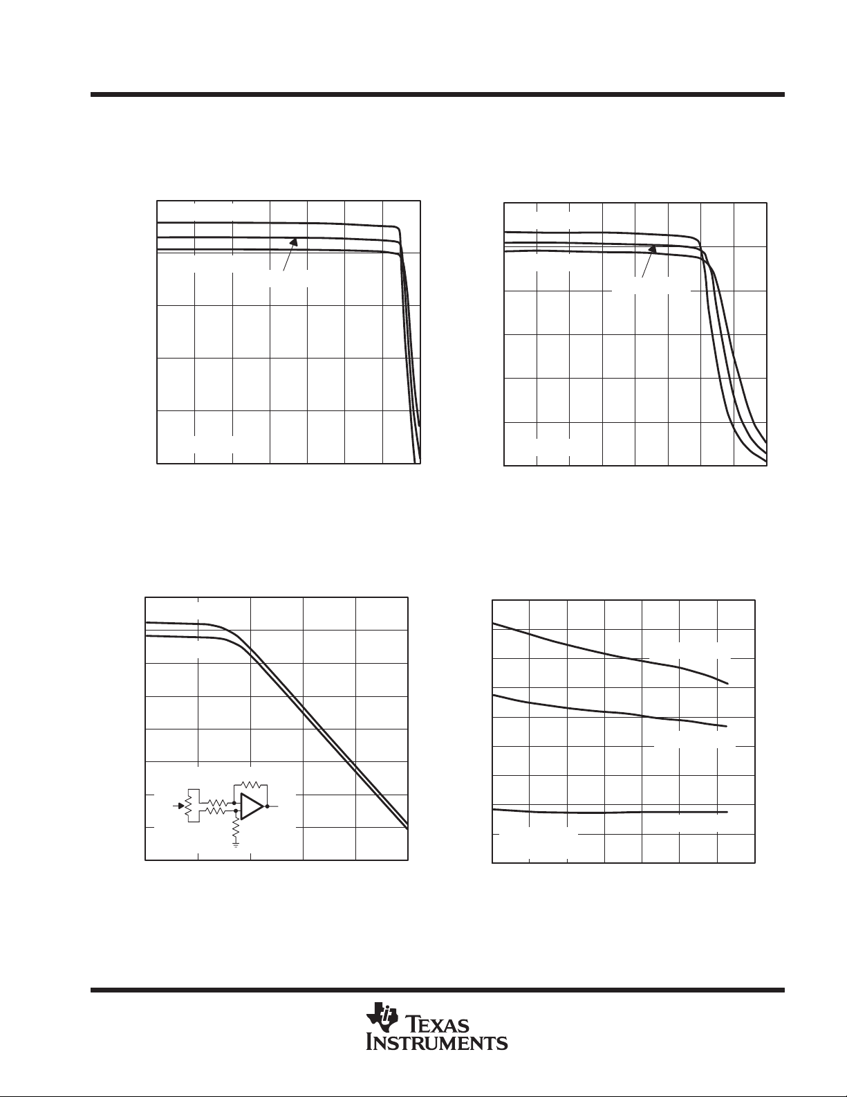
HARMONIC DISTORTION
PEAK-TO-PEAK OUTPUT VOLTAGE SWING
–50
8 MHz
Gain = 2
–55
VCC = ±15 V
RL = 150 Ω
RF = 750 Ω
–60
–65
–70
–75
Harmonic Distortion – dBc
–80
–85
0 2 4 6 12 14108 16
V
– Peak-to-Peak Output Voltage Swing – V
O(PP)
2nd Harmonic
Figure 18
HARMONIC DISTORTION
FREQUENCY
–70
Gain = 2
VCC = ±15 V
–75
–80
–85
VO = 2 V
RL = 150 Ω
RF = 750 Ω
PP
vs
3rd Harmonic
vs
3rd Harmonic
18
20
HARMONIC DISTORTION
PEAK-TO-PEAK OUTPUT VOLTAGE SWING
–50
4 MHz
Gain = 2
–55
VCC = ±15 V
RL = 150 Ω
–60
RF = 750 Ω
–65
–70
–75
–80
Harmonic Distortion – dBc
–85
–90
–95
0 2 4 6 12 14108 16
V
– Peak-to-Peak Output Voltage Swing – V
O(PP)
2nd Harmonic
Figure 19
HARMONIC DISTORTION
FREQUENCY
–60
Gain = 2
VCC = ±5 V
–65
–70
–75
–80
VO = 2 V
RL = 150 Ω
RF = 750 Ω
PP
vs
3rd Harmonic
vs
18
20
–90
Harmonic Distortion – dBc
–95
–100
100k 1M 10M
10
2nd Harmonic
f – Frequency – Hz
Figure 20
–85
–90
Harmonic Distortion – dBc
–95
–100
100k 1M 10M
POST OFFICE BOX 655303 • DALLAS, TEXAS 75265
2nd Harmonic
3rd Harmonic
f – Frequency – Hz
Figure 21

THS3001, THS3002
420-MHz HIGH-SPEED CURRENT-FEEDBACK AMPLIFIERS
SLOS217A – JULY 1998 – REVISED JUNE 1999
TYPICAL CHARACTERISTICS
DIFFERENTIAL GAIN
vs
LOADING
0.04
Gain = 2
RF = 750 Ω
40 IRE NTSC Modulation
Worst Case: ±100 IRE Ramp
0.03
VCC = ±15 V
0.02
VCC = ±5 V
Differential Gain – %
0.01
0
1234 78
Number of 150 Ω Loads
65
Figure 22
DIFFERENTIAL PHASE
vs
LOADING
0.3
Gain = 2
RF = 750 Ω
40 IRE NTSC Modulation
0.25
Worst Case: ±100 IRE Ramp
0.2
DIFFERENTIAL GAIN
vs
LOADING
0.04
Gain = 2
RF = 750 Ω
40 IRE PAL Modulation
Worst Case: ±100 IRE Ramp
0.03
VCC = ±15 V
0.02
VCC = ±5 V
Differential Gain – %
0.01
0
1234 78
Number of 150 Ω Loads
65
Figure 23
DIFFERENTIAL PHASE
vs
LOADING
0.35
Gain = 2
RF = 750 Ω
0.3
40 IRE PAL Modulation
Worst Case: ±100 IRE Ramp
0.25
0.15
VCC = ±15 V
0.1
Differential Phase – Degrees
0.05
0
1234 78
Number of 150 Ω Loads
VCC = ±5 V
65
Figure 24
POST OFFICE BOX 655303 • DALLAS, TEXAS 75265
0.2
0.15
0.1
Differential Phase – Degrees
0.05
0
1234 78
VCC = ±15 V
VCC = ±5 V
65
Number of 150 Ω Loads
Figure 25
11

THS3001, THS3002
420-MHz HIGH-SPEED CURRENT-FEEDBACK AMPLIFIERS
SLOS217A – JULY 1998 – REVISED JUNE 1999
TYPICAL CHARACTERISTICS
3
Gain = 1
VCC = ±15 V
2
RL = 150 Ω
VI = 200 mV RMS
1
0
–1
–2
–3
Output Amplitude – dB
–4
–5
–6
9
Gain = 2
VCC = ±15 V
8
RL = 150 Ω
7
VI = 200 mV RMS
OUTPUT AMPLITUDE
vs
FREQUENCY
RF = 750 Ω
RF = 1 kΩ
RF = 1.5 kΩ
1M 100M
10M 1G100k
f – Frequency – Hz
Figure 26
OUTPUT AMPLITUDE
vs
FREQUENCY
RF = 560 Ω
3
Gain = 1
VCC = ±5 V
2
RL = 150 Ω
VI = 200 mV RMS
1
0
–1
–2
–3
Output Amplitude – dB
–4
–5
–6
9
Gain = 2
VCC = ±5 V
8
RL = 150 Ω
7
VI = 200 mV RMS
OUTPUT AMPLITUDE
vs
FREQUENCY
RF = 750 Ω
RF = 1 kΩ
RF = 1.5 kΩ
1M 100M
10M 1G100k
f – Frequency – Hz
Figure 27
OUTPUT AMPLITUDE
vs
FREQUENCY
RF = 560 Ω
6
5
4
3
2
Output Amplitude – dB
1
0
–1
12
RF = 680 Ω
RF = 1 kΩ
1M 100M
10M 1G100k
f – Frequency – Hz
Figure 28
POST OFFICE BOX 655303 • DALLAS, TEXAS 75265
6
5
4
3
2
Output Amplitude – dB
1
0
–1
RF = 750 Ω
RF = 1 kΩ
1M 100M
10M 1G100k
f – Frequency – Hz
Figure 29

THS3001, THS3002
420-MHz HIGH-SPEED CURRENT-FEEDBACK AMPLIFIERS
SLOS217A – JULY 1998 – REVISED JUNE 1999
TYPICAL CHARACTERISTICS
OUTPUT AMPLITUDE
vs
FREQUENCY
70
60
50
40
30
20
Output Amplitude – dB
10
0
–10
NORMALIZED OUTPUT RESPONSE
vs
FREQUENCY
3
Gain = –1
VCC = ±15 V
2
RL = 150 Ω
VI = 200 mV RMS
1
RF = 560 Ω
VCC = ±5 V
G = +1000
RF = 10 kΩ
RL = 150 Ω
VO = 200 mV RMS
1M 100M
10M 1G100k
f – Frequency – Hz
Figure 30
VCC = ±15 V
3
2
1
NORMALIZED OUTPUT RESPONSE
vs
FREQUENCY
Gain = –1
VCC = ±5 V
RL = 150 Ω
VI = 200 mV RMS
RF = 560 Ω
0
–1
–2
–3
–4
Normalized Output Response – dB
–5
–6
1M 100M
f – Frequency – Hz
RF = 680 Ω
10M 1G100k
Figure 31
RF = 1 kΩ
POST OFFICE BOX 655303 • DALLAS, TEXAS 75265
0
–1
–2
–3
–4
Normalized Output Response – dB
–5
–6
1M 100M
f – Frequency – Hz
RF = 750 Ω
10M 1G100k
Figure 32
RF = 1 kΩ
13

THS3001, THS3002
420-MHz HIGH-SPEED CURRENT-FEEDBACK AMPLIFIERS
SLOS217A – JULY 1998 – REVISED JUNE 1999
TYPICAL CHARACTERISTICS
NORMALIZED OUTPUT RESPONSE
vs
FREQUENCY
3
RF = 390 Ω
0
–3
–6
–9
Normalized Output Response – dB
Gain = +5
–12
VCC = ±15 V
RL = 150 Ω
VO = 200 mV RMS
–15
1M 100M
f – Frequency – Hz
RF = 560 Ω
10M 1G100k
Figure 33
SMALL AND LARGE SIGNAL
FREQUENCY RESPONSE
–3
VI = 500 mV
–6
RF = 1 kΩ
NORMALIZED OUTPUT RESPONSE
vs
FREQUENCY
4
2
0
–2
–4
–6
–8
–10
Normalized Output Response – dB
Gain = +5
VCC = ±5 V
RL = 150 Ω
–12
VO = 200 mV RMS
–14
1M 100M
f – Frequency – Hz
RF = 620 Ω
10M 1G100k
Figure 34
SMALL AND LARGE SIGNAL
FREQUENCY RESPONSE
3
VI = 500 mV
0
RF = 390 Ω
RF = 1 kΩ
–9
VI = 250 mV
–12
–15
VI = 125 mV
–18
–21
Output Level – dBV
–24
–27
–30
VI = 62.5 mV
Gain = 1
VCC = ±15 V
RF = 1 kΩ
RL = 150 Ω
1M 100M
10M 1G100k
f – Frequency – Hz
Figure 35
–3
VI = 250 mV
–6
–9
VI = 125 mV
–12
–15
Output Level – dBV
–18
–21
–24
VI = 62.5 mV
Gain = 2
VCC = ±15 V
RF = 680 Ω
RL = 150 Ω
1M 100M
10M 1G100k
f – Frequency – Hz
Figure 36
14
POST OFFICE BOX 655303 • DALLAS, TEXAS 75265

THS3001, THS3002
420-MHz HIGH-SPEED CURRENT-FEEDBACK AMPLIFIERS
SLOS217A – JULY 1998 – REVISED JUNE 1999
TYPICAL CHARACTERISTICS
SMALL SIGNAL PULSE RESPONSE
300
100
–100
– Input Voltage – mV
–200
I
V
200
100
0
–100
– Output Voltage – V
–200
O
V
–300
0302010 40 50 7060 80 90 100
Gain = 1
VCC = ±5 V
RL = 150 Ω
RF = 1 kΩ
tr/tf = 300 ps
t – Time – ns
Figure 37
LARGE SIGNAL PULSE RESPONSE
3
SMALL SIGNAL PULSE RESPONSE
60
20
–20
– Input Voltage – mV
–60
I
V
200
100
0
–100
–200
– Output Voltage – mV
O
V
–300
0302010 40 50 7060 80 90 100
Gain = 5
VCC = ±5 V
RL = 150 Ω
RF = 1 kΩ
tr/tf = 300 ps
t – Time – ns
Figure 38
LARGE SIGNAL PULSE RESPONSE
3
1
–1
– Input Voltage – V
–3
I
V
2
1
0
–1
– Output Voltage – V
–2
O
V
–3
0302010 40 50 7060 80 90 100
Gain = +1
VCC = ±15 V
RL = 150 Ω
RF = 1 kΩ
tr/tf= 2.5 ns
t – Time – ns
Figure 39
1
–1
– Input Voltage – V
–3
I
V
2
1
0
–1
– Output Voltage – V
–2
O
V
–3
0302010 40 50 7060 80 90 100
Gain = 1
VCC = ±5 V
RL = 150 Ω
RF = 1 kΩ
tr/tf= 2.5 ns
t – Time – ns
Figure 40
POST OFFICE BOX 655303 • DALLAS, TEXAS 75265
15

THS3001, THS3002
420-MHz HIGH-SPEED CURRENT-FEEDBACK AMPLIFIERS
SLOS217A – JULY 1998 – REVISED JUNE 1999
TYPICAL CHARACTERISTICS
LARGE SIGNAL PULSE RESPONSE
3
1
–1
– Input Voltage – V
–3
I
V
10
5
0
–5
– Output Voltage – V
–10
O
V
–15
0302010 40 50 7060 80 90 100
Gain = +5
VCC = ±15 V
RL = 150 Ω
RF = 1 kΩ
tr/tf= 300 ps
t – Time – ns
Figure 41
LARGE SIGNAL PULSE RESPONSE
3
LARGE SIGNAL PULSE RESPONSE
600
200
–200
– Input Voltage – mV
–600
I
V
2
1
0
–1
– Output Voltage – V
–2
O
V
–3
0302010 40 50 7060 80 90 100
Gain = 5
VCC = ±5 V
RL = 150 Ω
RF = 1 kΩ
tr/tf= 300 ps
t – Time – ns
Figure 42
LARGE SIGNAL PULSE RESPONSE
3
1
–1
– Input Voltage – V
2
I
V
1
0
–1
–2
– Output Voltage – V
O
V
–3
0302010 40 50 7060 80 90 100
Gain = –1
VCC = ±15 V
RL = 150 Ω
RF = 1 kΩ
tr/tf= 2.5 ns
t – Time – ns
Figure 43
1
–1
– Input Voltage – V
2
I
V
1
0
–1
–2
– Output Voltage – V
O
V
–3
0302010 40 50 7060 80 90 100
Gain = –1
VCC = ±5 V
RL = 150 Ω
RF = 1 kΩ
tr/tf= 300 ps
t – Time – ns
Figure 44
16
POST OFFICE BOX 655303 • DALLAS, TEXAS 75265

THS3001, THS3002
420-MHz HIGH-SPEED CURRENT-FEEDBACK AMPLIFIERS
SLOS217A – JULY 1998 – REVISED JUNE 1999
TYPICAL CHARACTERISTICS
LARGE SIGNAL PULSE RESPONSE
600
200
–200
– Input Voltage – mV
–600
I
V
2
1
0
–1
– Output Voltage – V
–2
O
V
–3
0302010 40 50 7060 80 90 100
Gain = –5
VCC = ±5 V
RL = 150 Ω
RF = 1 kΩ
tr/tf= 300 ps
t – Time – ns
Figure 45
LARGE SIGNAL PULSE RESPONSE
3
1
–1
– Input Voltage – V
–2
I
V
10
5
0
–5
– Output Voltage – V
–10
O
V
–15
0302010 40 50 7060 80 90 100
Gain = –5
VCC = ±15 V
RL = 150 Ω
RF = 1 kΩ
tr/tf= 300 ps
t – Time – ns
Figure 46
POST OFFICE BOX 655303 • DALLAS, TEXAS 75265
17

THS3001, THS3002
420-MHz HIGH-SPEED CURRENT-FEEDBACK AMPLIFIERS
SLOS217A – JULY 1998 – REVISED JUNE 1999
APPLICATION INFORMATION
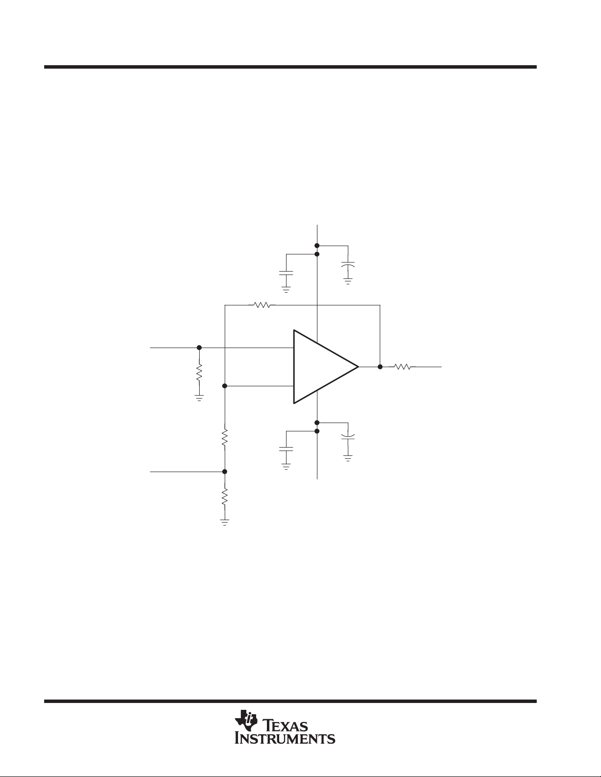
theory of operation
The THS300x is a high-speed, operational amplifier configured in a voltage-feedback architecture. The device
is built using a 30-V, dielectrically isolated, complementary bipolar process with NPN and PNP transistors
possessing f
has a wide bandwidth, high slew rate, fast settling time, and low distortion. A simplified schematic is shown in
Figure 47.
I
s of several GHz. This configuration implements an exceptionally high-performance amplifier that
T
V
CC+
7
IB
32
IN+ IN–
I
IB
Figure 47. Simplified Schematic
4
V
CC–
6
OUT
18
POST OFFICE BOX 655303 • DALLAS, TEXAS 75265

THS3001, THS3002
420-MHz HIGH-SPEED CURRENT-FEEDBACK AMPLIFIERS
SLOS217A – JULY 1998 – REVISED JUNE 1999
APPLICATION INFORMATION
recommended feedback and gain resistor values
The THS300x is fabricated using Texas Instruments 30-V complementary bipolar process, HVBiCOM. This
process provides the excellent isolation and extremely high slew rates that result in superior distortion
characteristics.
As with all current-feedback amplifiers, the bandwidth of the THS300x is an inversely proportional function of
the value of the feedback resistor (see Figures 26 to 34). The recommended resistors for the optimum frequency
response are shown in Table 1. These should be used as a starting point and once optimum values are found,
1% tolerance resistors should be used to maintain frequency response characteristics. For most applications,
a feedback resistor value of 1 kΩ is recommended – a good compromise between bandwidth and phase margin
that yields a very stable amplifier.
Consistent with current-feedback amplifiers, increasing the gain is best accomplished by changing the gain
resistor, not the feedback resistor . This is because the bandwidth of the amplifier is dominated by the feedback
resistor value and internal dominant-pole capacitor. The ability to control the amplifier gain independent of the
bandwidth constitutes a major advantage of current-feedback amplifiers over conventional voltage-feedback
amplifiers. Therefore, once a frequency response is found suitable to a particular application, adjust the value
of the gain resistor to increase or decrease the overall amplifier gain.
Finally, it is important to realize the effects of the feedback resistance on distortion. Increasing the resistance
decreases the loop gain and increases the distortion. It is also important to know that decreasing load
impedance increases total harmonic distortion (THD). Typically, the third-order harmonic distortion increases
more than the second-order harmonic distortion.
Table 1. Recommended Resistor Values for Optimum Frequency Response
GAIN RF for VCC = ±15 V RF for VCC = ±5 V
1 1 kΩ 1 kΩ
2, –1 680 Ω 750 Ω
–2 620 Ω 620 Ω
5 560 Ω 620 Ω
offset voltage
The output offset voltage, (VOO) is the sum of the input offset voltage (VIO) and both input bias currents (IIB) times
the corresponding gains. The following schematic and formula can be used to calculate the output offset
voltage:
R
F
I
R
G
R
S
IB–
+
V
IO
–
+
V
O
VOO+
I
IB+
R
V
ǒ
IO
Figure 48. Output Offset Voltage Model
F
1
) ǒ
Ǔ
"
I
Ǔ
R
G
POST OFFICE BOX 655303 • DALLAS, TEXAS 75265
R
IB
ǒ
)
S
1
) ǒ
R
F
Ǔ
Ǔ
R
G
"
I
IB–RF
19

THS3001, THS3002
420-MHz HIGH-SPEED CURRENT-FEEDBACK AMPLIFIERS
SLOS217A – JULY 1998 – REVISED JUNE 1999
APPLICATION INFORMATION
noise calculations and noise figure
Noise can cause errors on very small signals. This is especially true for amplifying small signals coming over
a transmission line or an antenna. The noise model for current-feedback amplifiers (CFB) is the same as for
voltage feedback amplifiers (VFB). The only difference between the two is that CFB amplifiers generally specify
different current-noise parameters for each input, while VFB amplifiers usually only specify one noise-current
parameter. The noise model is shown in Figure 49. This model includes all of the noise sources as follows:
• e
= amplifier internal voltage noise (nV/√Hz)
n
• IN+ = noninverting current noise (pA/√Hz)
• IN– = inverting current noise (pA/√Hz)
• e
The total equivalent input noise density (eni) is calculated by using the following equation:
Where:
= thermal voltage noise associated with each resistor (eRx = 4 kTRx)
Rx
e
eni+
e
)ǒIN
Rs
)
R
S
ni
Ǹ
2
ǒ
Ǔ
e
n
k = Boltzmann’s constant = 1.380658 × 10
T = temperature in degrees Kelvin (273 +°C)
R
|| RG = parallel resistance of RF and R
F
e
n
IN+
IN–
Figure 49. Noise Model
2
Ǔ
)
ǒ
IN–
R
S
Noiseless
+
_
e
Rf
e
Rg
R
G
ǒRFø
R
–23
G
R
F
2
Ǔ
Ǔ
)
G
4kTRs)
e
no
ǒ
4kT
RFø
R
G
Ǔ
To get the equivalent output noise of the amplifier, just multiply the equivalent input noise density (eni) by the
overall amplifier gain (A
eno+
20
eniAV+
).
V
R
ǒ
e
ni
F
1
Ǔ
)
POST OFFICE BOX 655303 • DALLAS, TEXAS 75265
(Noninverting Case)
R
G

THS3001, THS3002
420-MHz HIGH-SPEED CURRENT-FEEDBACK AMPLIFIERS
SLOS217A – JULY 1998 – REVISED JUNE 1999
APPLICATION INFORMATION
noise calculations and noise figure (continued)
As the previous equations show, to keep noise at a minimum, small value resistors should be used. As the
closed-loop gain is increased (by reducing R
resistance term. This leads to the general conclusion that the most dominant noise sources are the source
resistor (R
method, noise sources smaller than 25% of the largest noise source can be effectively ignored. This can greatly
simplify the formula and make noise calculations much easier.
This brings up another noise measurement usually preferred in RF applications, the noise figure (NF). Noise
figure is a measure of noise degradation caused by the amplifier. The value of the source resistance must be
defined and is typically 50 Ω in RF applications.
Because the dominant noise components are generally the source resistance and the internal amplifier noise
voltage, we can approximate noise figure as:
) and the internal amplifier noise voltage (en). Because noise is summed in a root-mean-squares
S
2
e
NF
+
10log
ȱ
ȧ
Ȳ
ȳ
ni
ȧ
e
2
Rs
ȴ
), the input noise is reduced considerably because of the parallel
G
2
Ǔ
ǒ
)
IN
4kTR
)
S
ǒ
e
n
NF
+
10log
ȱ
ȧ
ȧ
ȧ
ȧ
ȧ
ȡ
ȧ
Ȣ
1
)
Ȳ
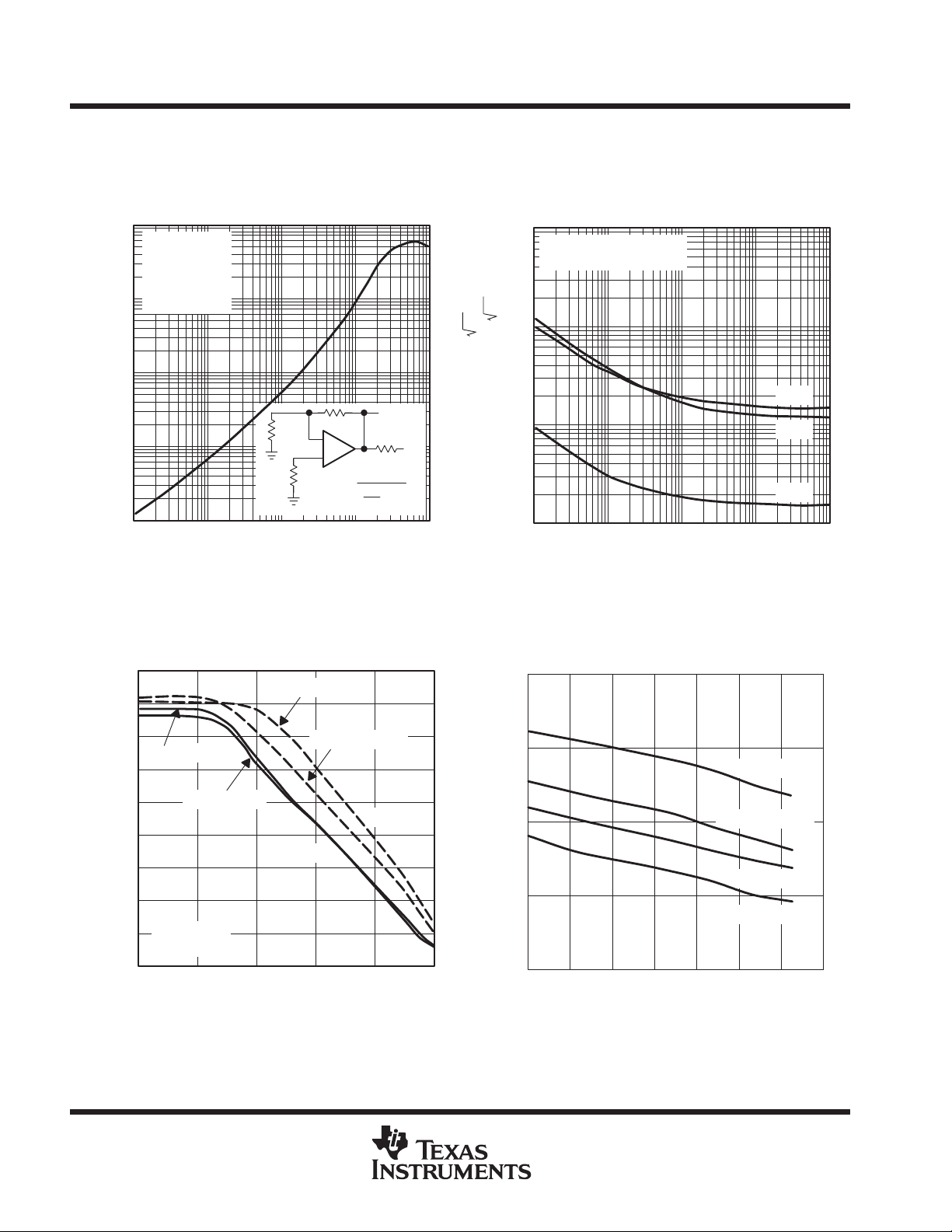
The Figure 50 shows the noise figure graph for the THS300x.
NOISE FIGURE
SOURCE RESISTANCE
20
f = 10 kHz
18
TA = 25°C
16
14
12
10
8
Noise Figure – dB
6
R
S
vs
2
ȳ
ȣ
Ǔ
ȧ
ȧ
Ȥ
ȧ
ȧ
ȧ
ȧ
ȴ
4
2
0
10 100 10k
RS – Source Resistance – Ω
Figure 50. Noise Figure vs Source Resistance
POST OFFICE BOX 655303 • DALLAS, TEXAS 75265
1k
21

THS3001, THS3002
420-MHz HIGH-SPEED CURRENT-FEEDBACK AMPLIFIERS
SLOS217A – JULY 1998 – REVISED JUNE 1999
APPLICATION INFORMATION
slew rate
The slew rate performance of a current-feedback amplifier, like the THS300x, is affected by many different
factors. Some of these factors are external to the device, such as amplifier configuration and PCB parasitics,
and others are internal to the device, such as available currents and node capacitance. Understanding some
of these factors should help the PCB designer arrive at a more optimum circuit with fewer problems.
Whether the THS300x is used in an inverting amplifier configuration or a noninverting configuration can impact
the output slew rate. As can be seen from the specification tables as well as some of the figures in this data sheet,
slew-rate performance in the inverting configuration is faster than in the noninverting configuration. This is
because in the inverting configuration the input terminals of the amplifier are at a virtual ground and do not
significantly change voltage as the input changes. Consequently , the time to charge any capacitance on these
input nodes is less than for the noninverting configuration, where the input nodes actually do change in voltage
an amount equal to the size of the input step. In addition, any PCB parasitic capacitance on the input nodes
degrades the slew rate further simply because there is more capacitance to charge. Also, if the supply voltage
(V
) to the amplifier is reduced, slew rate decreases because there is less current available within the amplifier
CC
to charge the capacitance on the input nodes as well as other internal nodes.
Internally , the THS300x has other factors that impact the slew rate. The amplifier’s behavior during the slew-rate
transition varies slightly depending upon the rise time of the input. This is because of the way the input stage
handles faster and faster input edges. Slew rates (as measured at the amplifier output) of less than about
1500 V/µs are processed by the input stage in a very linear fashion. Consequently, the output waveform
smoothly transitions between initial and final voltage levels. This is shown in Figure 51. For slew rates greater
than 1500 V/µs, additional slew-enhancing transistors present in the input stage begin to turn on to support
these faster signals. The result is an amplifier with extremely fast slew-rate capabilities. Figures 41 and 52 show
waveforms for these faster slew rates. The additional aberrations present in the output waveform with these
faster-slewing input signals are due to the brief saturation of the internal current mirrors. This phenomenon,
which typically lasts less than 20 ns, is considered normal operation and is not detrimental to the device in any
way . If for any reason this type of response is not desired, then increasing the feedback resistor or slowing down
the input-signal slew rate reduces the effect.
SLEW RATE
4
2
0
– Input Voltage – V
10
I
V
5
SR = 1500 V/µs
0
–5
–10
– Output Voltage – V
O
V
–15
0604020 80 100 140120 160 180 200
Gain = 5
VCC = ±15 V
RL = 150 Ω
RF = 1 kΩ
tr/tf = 10 ns
t – Time – ns
Figure 51
SLEW RATE
4
2
0
– Input Voltage – V
–2
I
V
5
0
–5
–10
– Output Voltage – V
O
V
–15
0604020 80 100 140120 160 180 200
SR = 2400 V/µs
Gain = 5
VCC = ±15 V
RL = 150 Ω
RF = 1 kΩ
tr/tf = 5 ns
t – Time – ns
Figure 52
22
POST OFFICE BOX 655303 • DALLAS, TEXAS 75265

THS3001, THS3002
420-MHz HIGH-SPEED CURRENT-FEEDBACK AMPLIFIERS
SLOS217A – JULY 1998 – REVISED JUNE 1999
APPLICATION INFORMATION
driving a capacitive load
Driving capacitive loads with high-performance amplifiers is not a problem as long as certain precautions are
taken. The first is to realize that the THS300x has been internally compensated to maximize its bandwidth and
slew-rate performance. When the amplifier is compensated in this manner, capacitive loading directly on the
output will decrease the device’s phase margin leading to high-frequency ringing or oscillations. Therefore, for
capacitive loads of greater than 10 pF, it is recommended that a resistor be placed in series with the output of
the amplifier, as shown in Figure 53. A minimum value of 20 Ω should work well for most applications. For
example, in 75-Ω transmission systems, setting the series resistor value to 75 Ω both isolates any capacitance
loading and provides the proper line impedance matching at the source end.
1 kΩ
1 kΩ
Input
_
THS300x
+
20 Ω
C
LOAD
Output
Figure 53. Driving a Capacitive Load
PCB design considerations
Proper PCB design techniques in two areas are important to assure proper operation of the THS300x. These
areas are high-speed layout techniques and thermal-management techniques. Because the THS300x is a
high-speed part, the following guidelines are recommended.
D
Ground plane – It is essential that a ground plane be used on the board to provide all components with a
low inductive ground connection. Although a ground connection directly to a terminal of the THS300x is not
necessarily required, it is recommended that the thermal pad of the package be tied to ground. This serves
two functions: it provides a low inductive ground to the device substrate to minimize internal crosstalk, and
it provides the path for heat removal.
D
Input stray capacitance – To minimize potential problems with amplifier oscillation, the capacitance at the
inverting input of the amplifiers must be kept to a minimum. T o do this, PCB trace runs to the inverting input
must be as short as possible, the ground plane must be removed under any etch runs connected to the
inverting input, and external components should be placed as close as possible to the inverting input. This
is especially true in the noninverting configuration. An example of this can be seen in Figure 54, which shows
what happens when a 1-pF capacitor is added to the inverting input terminal. The bandwidth increases at
the expense of peaking. This is because some of the error current is flowing through the stray capacitor
instead of the inverting node of the amplifier. Although, while the device is in the inverting mode, stray
capacitance at the inverting input has a minimal effect. This is because the inverting node is at a
ground
seen in Figure 55, where a 10-pF capacitor adds only 0.35 dB of peaking. In general, as the gain of the
system increases, the output peaking due to this capacitor decreases. While this can initially look like a
faster and better system, overshoot and ringing are more likely to occur under fast transient conditions. So
proper analysis of adding a capacitor to the inverting input node should be performed for stable operation.
and the voltage does not fluctuate nearly as much as in the noninverting configuration. This can be
virtual
POST OFFICE BOX 655303 • DALLAS, TEXAS 75265
23

THS3001, THS3002
420-MHz HIGH-SPEED CURRENT-FEEDBACK AMPLIFIERS
SLOS217A – JULY 1998 – REVISED JUNE 1999
APPLICATION INFORMATION
PCB design considerations (continued)
OUTPUT AMPLITUDE
vs
FREQUENCY
7
6
C
5
V
in
4
3
2
1
0
Output Amplitude – dB
–1
–2
Gain = 1
VCC = ±15 V
–3
VO = 200 mV RMS
–4
100k 10M 100M
1 kΩ
in
–
+
50 Ω
1M
V
out
RL =
150 Ω
f – Frequency – Hz
CI = 1 pF
CI = 0 pF
(Stray C Only)
1G
1
0
–1
–2
V
in
–3
–4
–5
Output Amplitude – dB
–6
Gain = –1
VCC = ±15 V
–7
VO = 200 mV RMS
–8
100k 10M 100M
Figure 54
D
Proper power-supply decoupling – Use a minimum 6.8-µF tantalum capacitor in parallel with a 0.1-µF
OUTPUT AMPLITUDE
vs
FREQUENCY
CI = 10 pF
CI = Stray C Only
C
in
1 kΩ
50 Ω
1 kΩ
–
+
1M
f – Frequency – Hz
RL =
150 Ω
Figure 55
V
out
ceramic capacitor on each supply terminal. It may be possible to share the tantalum among several
amplifiers depending on the application, but a 0.1-µF ceramic capacitor should always be used on the
supply terminal of every amplifier. In addition, the 0.1- µF capacitor should be placed as close as possible
to the supply terminal. As this distance increases, the inductance in the connecting etch makes the capacitor
less effective. The designer should strive for distances of less than 0.1 inches between the device power
terminal and the ceramic capacitors.
1G
thermal information
The THS300x incorporates output-current-limiting protection. Should the output become shorted to ground, the
output current is automatically limited to the value given in the data sheet. While this protects the output against
excessive current, the device internal power dissipation increases due to the high current and large voltage drop
across the output transistors. Continuous output shorts are not recommended and could damage the device.
Additionally, connection of the amplifier output to one of the supply rails (±V
of the device is possible under this condition and should be avoided. But, the THS300x does not incorporate
thermal-shutdown protection. Because of this, special attention must be paid to the device’s power dissipation
or failure may result.
24
POST OFFICE BOX 655303 • DALLAS, TEXAS 75265
) is not recommended. Failure
CC

THS3001, THS3002
420-MHz HIGH-SPEED CURRENT-FEEDBACK AMPLIFIERS
SLOS217A – JULY 1998 – REVISED JUNE 1999
APPLICATION INFORMATION
thermal information (continued)
The thermal coefficient θJA is approximately 169°C/W for the SOIC 8-pin D package. For a given θJA, the
maximum power dissipation, shown in Figure 56, is calculated by the following formula:
T
MAX–TA
Where:
ǒ
PD+
P
= Maximum power dissipation of THS300x (watts)
D
T
= Absolute maximum junction temperature (150°C)
MAX
T
= Free-ambient air temperature (°C)
A
θ
= Thermal coefficient from die junction to ambient air (°C/W)
JA
q
JA
1.5
Ǔ
MAXIMUM POWER DISSIPATION
vs
FREE-AIR TEMPERATURE
SOIC-D Package:
θJA = 169°C/W
TJ = 150°C
No Airflow
1
0.5
– Maximum Power Dissipation – W
D
P
0
–20 20
Figure 56. Maximum Power Dissipation vs Free-Air Temperature
0 40 100–40
TA – Free-Air Temperature – ° C
60 80
POST OFFICE BOX 655303 • DALLAS, TEXAS 75265
25

THS3001, THS3002
420-MHz HIGH-SPEED CURRENT-FEEDBACK AMPLIFIERS
SLOS217A – JULY 1998 – REVISED JUNE 1999
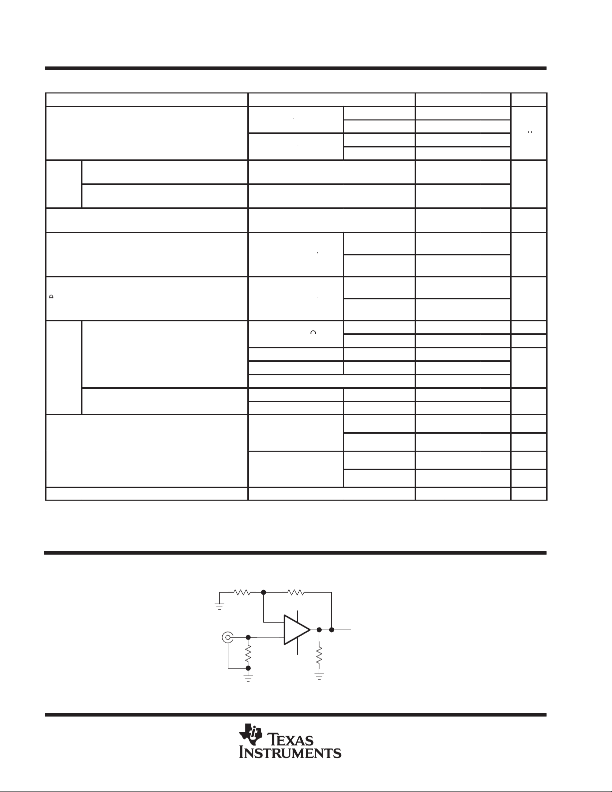
APPLICATION INFORMATION
general configurations
A common error for the first-time CFB user is the creation of a unity gain buffer amplifier by shorting the output
directly to the inverting input. A CFB amplifier in this configuration will oscillate and is not recommended. The
THS300x, like all CFB amplifiers, must have a feedback resistor for stable operation. Additionally, placing
capacitors directly from the output to the inverting input is not recommended. This is because, at high
frequencies, a capacitor has a very low impedance. This results in an unstable amplifier and should not be
considered when using a current-feedback amplifier. Because of this, integrators and simple low-pass filters,
which are easily implemented on a VFB amplifier, have to be designed slightly dif ferently . If filtering is required,
simply place an RC-filter at the noninverting terminal of the operational-amplifier (see Figure 57).
R
G
V
I
R1
C1
R
F
–
+
V
O
f
–3dB
V
O
+ ǒ
V
I
+
1
)
1
2pR1C1
R
F
ǒ
Ǔ
R
G
1)sR1C1
1
Ǔ
Figure 57. Single-Pole Low-Pass Filter
If a multiple-pole filter is required, the use of a Sallen-Key filter can work very well with CFB amplifiers. This is
because the filtering elements are not in the negative feedback loop and stability is not compromised. Because
of their high slew-rates and high bandwidths, CFB amplifiers can create very accurate signals and help minimize
distortion. An example is shown in Figure 58.
C1
V
I
R2R1
C2
R
G
+
_
R
F
R1 = R2 = R
C1 = C2 = C
Q = Peaking Factor
(Butterworth Q = 0.707)
1
+
2pRC
R
F
1
2 –
(
)
Q
R
f
–3dB
G
=
Figure 58. 2-Pole Low-Pass Sallen-Key Filter
There are two simple ways to create an integrator with a CFB amplifier. The first, shown in Figure 59, adds a
resistor in series with the capacitor. This is acceptable because at high frequencies, the resistor is dominant
and the feedback impedance never drops below the resistor value. The second, shown in Figure 60, uses
positive feedback to create the integration. Caution is advised because oscillations can occur due to the positive
feedback.
26
POST OFFICE BOX 655303 • DALLAS, TEXAS 75265

general configurations (continued)
THS3001, THS3002
420-MHz HIGH-SPEED CURRENT-FEEDBACK AMPLIFIERS
SLOS217A – JULY 1998 – REVISED JUNE 1999
APPLICATION INFORMATION
–
+
C1
THS300x
R
F
R
V
I
G
Figure 59. Inverting CFB Integrator
C1
R
F
–
+
R2R1
R
G
THS300x
V
I
R
A
Figure 60. Noninverting CFB Integrator
V
O
+ ǒ
V
V
O
V
O
I
For Stable Operation:
VO
R
R
R2
R1 || R
≅ V
I
F
G
(
ȡ
Ǔ
ȧ
Ȣ
A
1 +
sR1C1
≥
RFC1
S
R
R
R
F
R
G
ȣ
ȧ
Ȥ
F
G
)
1
S
)
The THS300x may also be employed as a very good video distribution amplifier. One characteristic of
distribution amplifiers is the fact that the differential phase (DP) and the differential gain (DG) are compromised
as the number of lines increases and the closed-loop gain increases (see Figures 22 to 25 for more information).
Be sure to use termination resistors throughout the distribution system to minimize reflections and capacitive
loading.
750 Ω750 Ω
–
V
I
+
THS300x
75 Ω
75 Ω
N Lines
75 Ω
75-Ω Transmission Line
75 Ω
75 Ω
V
O1
V
ON
Figure 61. Video Distribution Amplifier Application
POST OFFICE BOX 655303 • DALLAS, TEXAS 75265
27
THS3001, THS3002
420-MHz HIGH-SPEED CURRENT-FEEDBACK AMPLIFIERS
SLOS217A – JULY 1998 – REVISED JUNE 1999
APPLICATION INFORMATION
evaluation board
Evaluation boards are available for the THS3001 (literature #SLOP130) and the THS3002 (literature
#SLOP241). The boards have been configured for very low parasitic capacitance in order to realize the full
performance of the amplifier. Schematics of the evaluation boards are shown in Figures 62 and 63. The circuitry
has been designed so that the amplifier may be used in either an inverting or noninverting configuration. T o order
the evaluation board contact your local TI sales office or distributor . For more detailed information, refer to the
THS3001 EVM User’s Manual
To order the evaluation board, contact your local TI sales office or distributor.
(literature #SLOV021) or the
VCC+
C2
0.1 µF
THS3002 EVM User’s Guide
+
C1
6.8 µF
(literature #SLOVxxx).
IN+
IN–
R1
1 kΩ
+
R3
49.9 Ω
R5
1 kΩ
R4
49.9 Ω
C4
0.1 µF
THS3001
_
VCC–
C3
6.8 µF
+
Figure 62. THS3001 Evaluation Board Schematic
R2
49.9 Ω
OUT
28
POST OFFICE BOX 655303 • DALLAS, TEXAS 75265
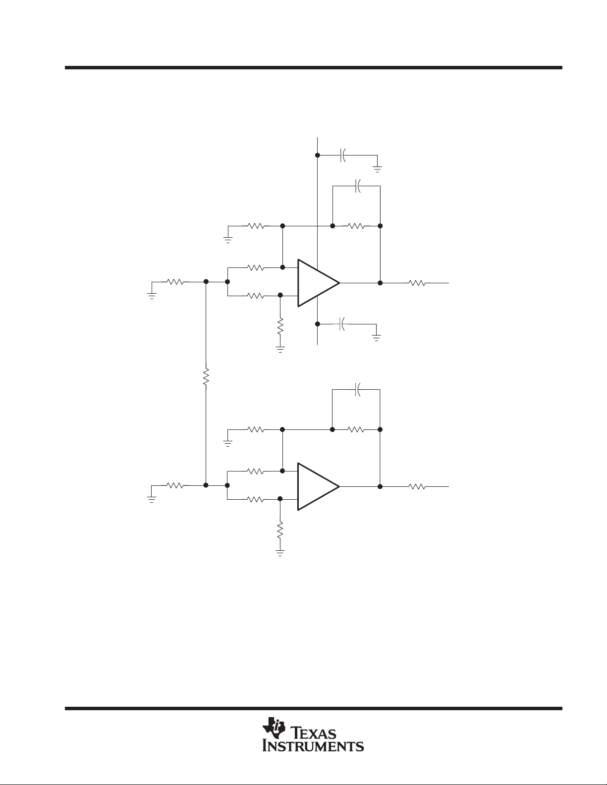
evaluation board (continued)
THS3001, THS3002
420-MHz HIGH-SPEED CURRENT-FEEDBACK AMPLIFIERS
SLOS217A – JULY 1998 – REVISED JUNE 1999
APPLICATION INFORMATION
R1
100 Ω
R8
R5
R4
100 Ω
R3
100 Ω
R13
2
3
R2
0 Ω
–
+
VCC+
8
4
VCC–
C5
0.1 µF
301 Ω
THS3002
U1:A
1
C4
0.1 µF
R14
301 Ω
C3
R6
R7
49.9 Ω
OUT1
C6
R9
100 Ω
R12
100 Ω
R11
100 Ω
6
5
R10
0 Ω
–
+
THS3002
U1:B
7
R15
49.9 Ω
Figure 63. THS3002 Evaluation Board Schematic
OUT2
POST OFFICE BOX 655303 • DALLAS, TEXAS 75265
29

THS3001, THS3002
420-MHz HIGH-SPEED CURRENT-FEEDBACK AMPLIFIERS
SLOS217A – JULY 1998 – REVISED JUNE 1999
MECHANICAL INFORMATION
D (R-PDSO-G**) PLASTIC SMALL-OUTLINE PACKAGE
14 PIN SHOWN
14
1
0.069 (1,75) MAX
0.050 (1,27)
A
0.020 (0,51)
0.014 (0,35)
0.010 (0,25)
0.004 (0,10)
8
7
0.010 (0,25)
0.157 (4,00)
0.150 (3,81)
M
0.244 (6,20)
0.228 (5,80)
Seating Plane
0.004 (0,10)
PINS **
DIM
A MAX
A MIN
0.008 (0,20) NOM
Gage Plane
0°–8°
8
0.197
(5,00)
0.189
(4,80)
14
0.344
(8,75)
0.337
(8,55)
0.010 (0,25)
0.044 (1,12)
0.016 (0,40)
4040047/D 10/96
16
0.394
(10,00)
0.386
(9,80)
NOTES: A. All linear dimensions are in inches (millimeters).
B. This drawing is subject to change without notice.
C. Body dimensions do not include mold flash or protrusion, not to exceed 0.006 (0,15).
D. Falls within JEDEC MS-012
30
POST OFFICE BOX 655303 • DALLAS, TEXAS 75265

THS3001, THS3002
420-MHz HIGH-SPEED CURRENT-FEEDBACK AMPLIFIERS
SLOS217A – JULY 1998 – REVISED JUNE 1999
MECHANICAL INFORMATION
DGN (S-PDSO-G8) PowerPAD PLASTIC SMALL-OUTLINE PACKAGE
0,65
8
1
1,07 MAX
3,05
2,95
0,38
0,25
5
3,05
2,95
4
Seating Plane
0,15
0,05
0,25
4,98
4,78
M
0,10
Thermal Pad
(See Note D)
0,15 NOM
Gage Plane
0°–6°
0,25
0,69
0,41
NOTES: A. All linear dimensions are in millimeters.
B. This drawing is subject to change without notice.
C. Body dimensions include mold flash or protrusions.
D. The package thermal performance may be enhanced by attaching an external heat sink to the thermal pad. This pad is electrically
and thermally connected to the backside of the die and possibly selected leads.
E. Falls within JEDEC MO-187
PowerPAD is a trademark of Texas Instruments Incorporated.
4073271/A 01/98
POST OFFICE BOX 655303 • DALLAS, TEXAS 75265
31

IMPORTANT NOTICE
T exas Instruments and its subsidiaries (TI) reserve the right to make changes to their products or to discontinue
any product or service without notice, and advise customers to obtain the latest version of relevant information
to verify, before placing orders, that information being relied on is current and complete. All products are sold
subject to the terms and conditions of sale supplied at the time of order acknowledgement, including those
pertaining to warranty, patent infringement, and limitation of liability.
TI warrants performance of its semiconductor products to the specifications applicable at the time of sale in
accordance with TI’s standard warranty. Testing and other quality control techniques are utilized to the extent
TI deems necessary to support this warranty . Specific testing of all parameters of each device is not necessarily
performed, except those mandated by government requirements.
CERT AIN APPLICATIONS USING SEMICONDUCTOR PRODUCTS MAY INVOLVE POTENTIAL RISKS OF
DEATH, PERSONAL INJURY, OR SEVERE PROPERTY OR ENVIRONMENTAL DAMAGE (“CRITICAL
APPLICATIONS”). TI SEMICONDUCTOR PRODUCTS ARE NOT DESIGNED, AUTHORIZED, OR
WARRANTED TO BE SUITABLE FOR USE IN LIFE-SUPPORT DEVICES OR SYSTEMS OR OTHER
CRITICAL APPLICA TIONS. INCLUSION OF TI PRODUCTS IN SUCH APPLICATIONS IS UNDERST OOD TO
BE FULLY AT THE CUSTOMER’S RISK.
In order to minimize risks associated with the customer’s applications, adequate design and operating
safeguards must be provided by the customer to minimize inherent or procedural hazards.
TI assumes no liability for applications assistance or customer product design. TI does not warrant or represent
that any license, either express or implied, is granted under any patent right, copyright, mask work right, or other
intellectual property right of TI covering or relating to any combination, machine, or process in which such
semiconductor products or services might be or are used. TI’s publication of information regarding any third
party’s products or services does not constitute TI’s approval, warranty or endorsement thereof.
Copyright 1999, Texas Instruments Incorporated
 Loading...