


MULTICAM
MC-1134P Multimode
Very-High-Resolution B/W Camera
User’s Guide
JULY 1993
SOCU002C
B-1

Running Title—Attribute Reference
T exas Instruments (TI) reserves the right to make changes to its products or to discontinue any
semiconductor product or service without notice, and advises its customers to obtain the latest
version of relevant information to verify , before placing orders, that the information being relied
on is current.
TI warrants performance of its semiconductor products and related software to the specifications
applicable at the time of sale in accordance with TI’s standard warranty . T esting and other quality
control techniques are utilized to the extent TI deems necessary to support this warranty.
Specific testing of all parameters of each device is not necessarily performed, except those
mandated by government requirements.
Certain applications using semiconductor products may involve potential risks of death,
personal injury , or severe property or environmental damage (“Critical Applications”).
TI SEMICONDUCTOR PRODUCTS ARE NOT DESIGNED, INTENDED, AUTHORIZED, OR
WARRANTED TO BE SUITABLE FOR USE IN LIFE-SUPPORT APPLICATIONS, DEVICES
OR SYSTEMS OR OTHER CRITICAL APPLICATIONS.
Inclusion of TI products in such applications is understood to be fully at the risk of the customer.
Use of TI products in such applications requires the written approval of an appropriate TI officer .
Questions concerning potential risk applications should be directed to TI through a local SC
sales office.
IMPORTANT NOTICE
In order to minimize risks associated with the customer’s applications, adequate design and
operating safeguards should be provided by the customer to minimize inherent or procedural
hazards.
TI assumes no liability for applications assistance, customer product design, software
performance, or infringement of patents or services described herein. Nor does TI warrant or
represent that any license, either express or implied, is granted under any patent right, copyright,
mask work right, or other intellectual property right of TI covering or relating to any combination,
machine, or process in which such semiconductor products or services might be or are used.
Copyright 1994, Texas Instruments Incorporated
B-2

Running Title—Attribute Reference
Contents
1 General Description B-53. . . . . . . . . . . . . . . . . . . . . . . . . . . . . . . . . . . . . . . . . . . . . . . . . . . . . . . . . . . .
1.1 Features B-54. . . . . . . . . . . . . . . . . . . . . . . . . . . . . . . . . . . . . . . . . . . . . . . . . . . . . . . . . . . . . . . . .
1.2 Introduction B-54. . . . . . . . . . . . . . . . . . . . . . . . . . . . . . . . . . . . . . . . . . . . . . . . . . . . . . . . . . . . . . .
1.3 Equipment Supplied B-55. . . . . . . . . . . . . . . . . . . . . . . . . . . . . . . . . . . . . . . . . . . . . . . . . . . . . . .
2 Specifications B-57. . . . . . . . . . . . . . . . . . . . . . . . . . . . . . . . . . . . . . . . . . . . . . . . . . . . . . . . . . . . . . . . . .
2.1 Electrical B-58. . . . . . . . . . . . . . . . . . . . . . . . . . . . . . . . . . . . . . . . . . . . . . . . . . . . . . . . . . . . . . . . .
2.2 Mechanical B-58. . . . . . . . . . . . . . . . . . . . . . . . . . . . . . . . . . . . . . . . . . . . . . . . . . . . . . . . . . . . . . .
2.3 Absolute Maximum Ratings Over Operating Free-Air Temperature Range
2.4 Recommended Operating Conditions B-60. . . . . . . . . . . . . . . . . . . . . . . . . . . . . . . . . . . . . . . .
2.5 Electrical Characteristics B-60. . . . . . . . . . . . . . . . . . . . . . . . . . . . . . . . . . . . . . . . . . . . . . . . . . .
2.6 Handling Precautions B-60. . . . . . . . . . . . . . . . . . . . . . . . . . . . . . . . . . . . . . . . . . . . . . . . . . . . . .
(Unless Otherwise Noted) B-60. . . . . . . . . . . . . . . . . . . . . . . . . . . . . . . . . . . . . . . . . . . . . . . .
3 Installation B-61. . . . . . . . . . . . . . . . . . . . . . . . . . . . . . . . . . . . . . . . . . . . . . . . . . . . . . . . . . . . . . . . . . . . .
3.1 Connector Pin Functions B-62. . . . . . . . . . . . . . . . . . . . . . . . . . . . . . . . . . . . . . . . . . . . . . . . . . .
4 Operation B-63. . . . . . . . . . . . . . . . . . . . . . . . . . . . . . . . . . . . . . . . . . . . . . . . . . . . . . . . . . . . . . . . . . . . . .
4.1 General Operation B-64. . . . . . . . . . . . . . . . . . . . . . . . . . . . . . . . . . . . . . . . . . . . . . . . . . . . . . . . .
4.2 Camera Adjustment B-64. . . . . . . . . . . . . . . . . . . . . . . . . . . . . . . . . . . . . . . . . . . . . . . . . . . . . . . .
4.3 External Operation B-65. . . . . . . . . . . . . . . . . . . . . . . . . . . . . . . . . . . . . . . . . . . . . . . . . . . . . . . . .
4.3.1 VD IN and HD IN Waveforms B-65. . . . . . . . . . . . . . . . . . . . . . . . . . . . . . . . . . . . . . . .
4.3.2 VD IN and C-Sync Phase Relationship B-66. . . . . . . . . . . . . . . . . . . . . . . . . . . . . . . .
4.3.3 Delay and Jitter B-66. . . . . . . . . . . . . . . . . . . . . . . . . . . . . . . . . . . . . . . . . . . . . . . . . . . .
4.4 Mode Selection B-66. . . . . . . . . . . . . . . . . . . . . . . . . . . . . . . . . . . . . . . . . . . . . . . . . . . . . . . . . . . .
4.4.1 Sync Inputs/Outputs of Auxiliary Connector B-66. . . . . . . . . . . . . . . . . . . . . . . . . . . .
4.4.2 Mode Selection Function of Auxiliary Connector B-66. . . . . . . . . . . . . . . . . . . . . . . .
4.4.3 Description of Selectable Modes B-67. . . . . . . . . . . . . . . . . . . . . . . . . . . . . . . . . . . . . .
5 Circuit Description B-69. . . . . . . . . . . . . . . . . . . . . . . . . . . . . . . . . . . . . . . . . . . . . . . . . . . . . . . . . . . . .
5.1 Description of CCD Operation B-70. . . . . . . . . . . . . . . . . . . . . . . . . . . . . . . . . . . . . . . . . . . . . . .
6 Maintenance Instructions B-71. . . . . . . . . . . . . . . . . . . . . . . . . . . . . . . . . . . . . . . . . . . . . . . . . . . . . . .
6.1 Periodic Image Test B-72. . . . . . . . . . . . . . . . . . . . . . . . . . . . . . . . . . . . . . . . . . . . . . . . . . . . . . . .
6.2 Cleaning B-72. . . . . . . . . . . . . . . . . . . . . . . . . . . . . . . . . . . . . . . . . . . . . . . . . . . . . . . . . . . . . . . . . .
A Block Diagrams B-73. . . . . . . . . . . . . . . . . . . . . . . . . . . . . . . . . . . . . . . . . . . . . . . . . . . . . . . . . . . . . . . .
B Timing Diagrams B-79. . . . . . . . . . . . . . . . . . . . . . . . . . . . . . . . . . . . . . . . . . . . . . . . . . . . . . . . . . . . . . .
Chapter Title—Attribute Reference
B-3

Running Title—Attribute Reference
Figures
1–1 The MULTICAM MC-1134P Multimode Very-High-Resolution B/W Camera B-55. . . . . . . . . .
2–1 MC-1134P CCD Camera With Bottom-Mount Connector Option B-59. . . . . . . . . . . . . . . . . . . .
2–2 MC-1134P CCD Camera With Rear-Mount Connector Option B-59. . . . . . . . . . . . . . . . . . . . . .
A–1 CCD Timing/Power/Driver (TPD) Board Block Diagram B-74. . . . . . . . . . . . . . . . . . . . . . . . . . .
A–2 Video Processor Board Block Diagram B-75. . . . . . . . . . . . . . . . . . . . . . . . . . . . . . . . . . . . . . . . . .
A–3 TPD, Video Processor, and CCD Boards B-76. . . . . . . . . . . . . . . . . . . . . . . . . . . . . . . . . . . . . . . .
A–4 Interconnect Diagram for TPD Board, Video Processor Board, CCD Board,
B–1 Timing, High-Light Mode B-80. . . . . . . . . . . . . . . . . . . . . . . . . . . . . . . . . . . . . . . . . . . . . . . . . . . . . .
B–2 Timing, Low-Light Mode B-81. . . . . . . . . . . . . . . . . . . . . . . . . . . . . . . . . . . . . . . . . . . . . . . . . . . . . . .
B–3 Timing, Still Mode B-82. . . . . . . . . . . . . . . . . . . . . . . . . . . . . . . . . . . . . . . . . . . . . . . . . . . . . . . . . . . .
B–4 V Timing, Progressive-Scan Mode B-83. . . . . . . . . . . . . . . . . . . . . . . . . . . . . . . . . . . . . . . . . . . . . .
B–5 Horizontal Timing B-85. . . . . . . . . . . . . . . . . . . . . . . . . . . . . . . . . . . . . . . . . . . . . . . . . . . . . . . . . . . .
B–6 Serial Generator B-86. . . . . . . . . . . . . . . . . . . . . . . . . . . . . . . . . . . . . . . . . . . . . . . . . . . . . . . . . . . . .
B–7 Parallel Transfer – Field One B-86. . . . . . . . . . . . . . . . . . . . . . . . . . . . . . . . . . . . . . . . . . . . . . . . . .
B–8 Parallel Transfer – Field Two B-87. . . . . . . . . . . . . . . . . . . . . . . . . . . . . . . . . . . . . . . . . . . . . . . . . .
and Pin Connectors B-77. . . . . . . . . . . . . . . . . . . . . . . . . . . . . . . . . . . . . . . . . . . . . . . . . . . . . . . .
B-4

Chapter 1
General Description
Topic Page
1.1 Features B-6. . . . . . . . . . . . . . . . . . . . . . . . . . . . . . . . . . . . . . . . . . . . . . . . . . . . .
1.2 Introduction B-6. . . . . . . . . . . . . . . . . . . . . . . . . . . . . . . . . . . . . . . . . . . . . . . . . .
1.3 Equipment Supplied B-7. . . . . . . . . . . . . . . . . . . . . . . . . . . . . . . . . . . . . . . . . . .
Chapter Title—Attribute Reference
B-5

Features / Introduction
1.1 Features
1.2 Introduction
Texas Instruments has developed the first in a series of programmable video
cameras that utilize its very-high-resolution TC216 and TC217 CCD image
sensors. Features of the MC-1134P camera include:
-
RS-170 monochrome video format
-
High-quality image
-
1134 (H) x 486 (V) active picture elements
-
Internal or external synchronization
-
Factory-programmable timing to address specific customer needs
-
Small tubular package
The MULTICAM MC-1134P system is intended for scientific, medical, and
industrial image data-processing applications. The camera employs the T exas
Instruments TC217 frame-transfer CCD image sensor, which features
551,124 active photosites and can generate a very-high-resolution image. The
MUL TICAM MC-1134P system’s three modes of operation are user selectable
through an external connector provided with the system. The system is also
capable of internal or external synchronization through the same auxiliary
connector.
The MC-1134P camera has a standard C-mount that allows use of a variety
of lenses. The MULTICAM MC-1134P system provides signals for auto-iris
control via an external connector; the mating cable for this connector is
included in the MULTICAM package. The camera can be secured with the
1/4 x 20 tripod mount provided or it can be clamped externally.
The MC-1 134P series includes options for connector location, automatic gain
control (AGC), and gamma correction (0.45/1.0). Other options can be made
available upon customer request. The standard model part numbers are
shown in the following table.
PART NUMBER AGC GAMMA
MC-1134P Off 1 Bottom
MC-1134P-5 On 0.5 Bottom
MC-1134PB Off 1 Back
MC-1134PB-5 On 0.5 Back
CONNECTOR
LOCATION
B-6

Equipment Supplied
1.3 Equipment Supplied
The following items are shipped with each MULTICAM MC-1134P camera
system:
SYSTEM INVENTORY ITEM QTY
MC-1134P Multimode Very-High-Resolution B/W Camera 1
35-mm f1.7 C-Mount Lens 1
Infrared Filter (CM500) 1
PS1 Power Supply With Cable 1
Auto-Iris Motor Drive Cable 1
Auxiliary Connector 1
MULTICAM MC-1134P User’s Guide 1
Figure 1–1.The MULTICAM MC-1134P Multimode Very-High-Resolution B/W Camera
General Description
B-7

B-8

Chapter 2
Specifications
Topic Page
2.1 Electrical B-10. . . . . . . . . . . . . . . . . . . . . . . . . . . . . . . . . . . . . . . . . . . . . . . . . . . .
2.2 Mechanical B-10. . . . . . . . . . . . . . . . . . . . . . . . . . . . . . . . . . . . . . . . . . . . . . . . . .
2.3 Absolute Maximum Ratings Over Operating Free-Air
Temperature Range (Unless Otherwise Noted) B-12. . . . . . . . . . . . . . . . . .
2.4 Recommended Operating Conditions B-12. . . . . . . . . . . . . . . . . . . . . . . . . .
2.5 Electrical Characteristics B-12. . . . . . . . . . . . . . . . . . . . . . . . . . . . . . . . . . . . .
2.6 Handling Precautions B-12. . . . . . . . . . . . . . . . . . . . . . . . . . . . . . . . . . . . . . . .
Chapter Title—Attribute Reference
B-9

Electrical / Mechanical
2.1 Electrical
Faceplate Saturation Illumination
(Source Temperature = 2856 K) 0.5 lux. . . . . . . . . . . . .
Dynamic Range 60 dB. . . . . . . . . . . . . . . . . . . . . . . . . . .
Signal-to-Noise Ratio at 100 IRE
(photon noise limited) 45 dB. . . . . . . . . . . . . . . . . . . . . .
Blooming Protection more than 150X. . . . . . . . . . . . . . . . . . . . . . . .
Smear 0.12%. . . . . . . . . . . . . . . . . . . . . . . . . . . . . . . . . . . .
(timing as shown in Figure B–3)
AGC 8:1 or off. . . . . . . . . . . . . . . . . . . . . . . . . . . . . . . . . . . . .
Gamma 1.0 or 0.5. . . . . . . . . . . . . . . . . . . . . . . . . . . . . . . . . .
Synchronization internal or external. . . . . . . . . . . . . . . . . . . . . . . . . . .
Video Output Impedance 75 Ω. . . . . . . . . . . . . . . . . . .
Camera Power Consumption 4 W. . . . . . . . . . . . . . . .
2.2 Mechanical
Power Supply
Output Voltage 5 V dc, 12 V dc, –12 V dc. . . . . . . . . . . . . . . . . . . . .
Input Voltage 120 V ac @ 60 Hz. . . . . . . . . . . . . . . . . . . . . . .
Operating Free-Air Temperature Range –10°C to 40°C. . . . . . .
Storage Temperature Range –30°C to 70°C. . . . . . . . . . . . . . . .
Pixel Rate 21.47 MHz. . . . . . . . . . . . . . . . . . . . . . . . . . . . . . . .
Image Area Diagonal 11 mm. . . . . . . . . . . . . . . . . . . . . . .
Pixels Per Line 1,134. . . . . . . . . . . . . . . . . . . . . . . . . . . .
Pixel Size 7.8 µm x 13.6 µm. . . . . . . . . . . . . . . . . . . . . . . . . . . . . . . . .
Lens (C-Mount) 35 mm f1.7. . . . . . . . . . . . . . . . . . . . . . . . . . .
Tripod Mount 1/4 x 20 thread. . . . . . . . . . . . . . . . . . . . . . . . . . . . . .
Weight With Lens 17.15 oz. . . . . . . . . . . . . . . . . . . . . . . . . .
B-10
Weight Without Lens 11.85 oz. . . . . . . . . . . . . . . . . . . . . . .

Figure 2–1.MC-1134P CCD Camera With Bottom-Mount Connector Option
Mechanical
Optical Center Line
AUXPOWERVIDEOIRISTRIPOD
1.43
1.0
4.2
7.4
All dimensions are in inches.
Figure 2–2.MC-1134P CCD Camera With Rear-Mount Connector Option
IRISTRIPOD
0.45
1.75
POWER
AUX
VIDEO
1.75
All dimensions are in inches.
Specifications
B-1 1

Absolute / Recommended / Electrical / Handling
2.3 Absolute Maximum Ratings Over Operating Free-Air Temperature Range
(Unless Otherwise Noted)
Operating free-air temperature range –10°C to 40°C. . . . . . . . . . . . . . . . . . . . . . . . . . . . . . . . . . . . . .
Storage temperature range –30°C to 70°C. . . . . . . . . . . . . . . . . . . . . . . . . . . . . . . . . . . . . . . . . . . . . . .
2.4 Recommended Operating Conditions
MIN MAX UNIT
V
IH
V
IL
High-level input voltage 2 5.3 V
Low-level input voltage –0.3 0.8 V
2.5 Electrical Characteristics
PARAMETER TEST CONDITIONS MIN MAX UNIT
V
OH
V
OL
High-level output voltage IOH = –4 mA 2.4 V
Low-level output voltage IOL = 8 mA 0.45 V
2.6 Handling Precautions
The MC-1134P camera unit should be handled in accordance with standard
precautions for electro-optic equipment. The camera should not be
mishandled by dropping or by exposure to excessive moisture. When not in
use, the camera unit should be stored in a dust- and moisture-free
environment and within the specified storage-temperature range.
The MC-1134P camera unit contains electrostatic-discharge-sensitive
components and should be handled accordingly. Specific guidelines for
handling assemblies of this type are contained in the publication
for Handling Electrostatic-Discharge-Sensitive (ESDS) Devices and
Assemblies
Guidelines
available from Texas Instruments.
B-12

Chapter 3
Installation
Topic Page
3.1 Connector Pin Functions B-14. . . . . . . . . . . . . . . . . . . . . . . . . . . . . . . . . . . . .
Chapter Title—Attribute Reference
B-13
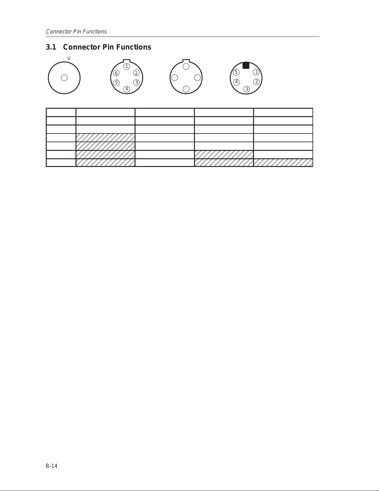
Connector Pin Functions
3.1 Connector Pin Functions
VIDEO
J20
6
5
AUXILIARY
1
2
3
4
J21 J22
POWER
1
4
2
3
IRIS
15
J23
4
2
3
PIN NO.
1 Video GND –12 V 12 V
2 Video Return SYNC I/O 12 V GND
3 Mode B 5 V Video Return
4 Mode A GND Video
5 V Drive NC
6 H Drive
VIDEO AUXILIARY POWER IRIS
Video Amphenol 31-10 BNC. . . . . . . . . . . . . . . . . . . . . .
Auxiliary Hirose SR30-10R-6S camera side. . . . . . . . . . . . . . . . . . . .
Hirose SR30-10PE-6P cable side
Power Hirose SR30-10R-4S camera side. . . . . . . . . . . . . . . . . . . . . .
Hirose SR30-10PE-4P cable side
Iris Hirose RP6-10R-5SA camera side. . . . . . . . . . . . . . . . . . . . . . . . .
Hirose RP6-10PG-5PA cable side
B-14

Chapter 4
Operation
Topic Page
4.1 General Operation B-16. . . . . . . . . . . . . . . . . . . . . . . . . . . . . . . . . . . . . . . . . . .
4.2 Camera Adjustment B-16. . . . . . . . . . . . . . . . . . . . . . . . . . . . . . . . . . . . . . . . . .
4.3 External Operation B-17. . . . . . . . . . . . . . . . . . . . . . . . . . . . . . . . . . . . . . . . . . .
4.4 Mode Selection B-18. . . . . . . . . . . . . . . . . . . . . . . . . . . . . . . . . . . . . . . . . . . . . .
Chapter Title—Attribute Reference
B-15

General Operation / Camera Adjustment
4.1 General Operation
The MC-1 134P operates as a self-contained unit requiring no inputs other than
the dc-power-supply input. The MC-1 134P is designed to operate with little or
no operator adjustment after the initial setup period.
The following conditions are required for general operation:
-
Power applied to the camera
-
Video cable connected to the camera
-
Sufficient lighting provided
-
Camera aimed at the desired subject
-
Lens focus and aperture rings adjusted for the subject
4.2 Camera Adjustment
The MC-1134P requires no internal adjustments. The only external
adjustments required in normal operation are to the lens focus and aperture.
These adjustments are dependent upon the scene being viewed.
The MC-1134P camera can be operated in either internal or external sync
mode. Internal sync mode is the default mode and requires no additional
connections. External sync mode operation requires that pin 2 on the auxiliary
connector be grounded. Vertical and horizontal drive signals should then be
applied to auxiliary connector pins 4 and 5, respectively . These drive signals
should not exceed CMOS voltage levels.
B-16

4.3 External Operation
Odd Field
VD In
HD In
External Operation
T
Even Field
No reset during even field. Camera does not recognize a VD In if it coincides with 63.5/2
µs.
–2 µs < T < 2 µs
Table 4–1.Synchronous Frequency Ranges
FREQUENCY RANGE MIN TYP MAX UNIT
Horizontal 15.710 15.734 15.759 kHz
Vertical 59.85 59.94 60.03 Hz
4.3.1 VD IN and HD IN Waveforms
1/f(H)
HD In
Not Critical
1/f(V)
VD In
Not Critical
Operation
B-17

External Operation / Mode Selection
MODE
4.3.2 VD IN and C-Sync Phase Relationship
VD (input)
C-Sync
4.3.3 Delay and Jitter
HD or
VD
C-Syn
c
Delay for HD In:
Delay for VD In:
C-Sync Jitter:
Dela
y
TTL Level
1H 9H
Jitte
r
180 ns (typ), 190 ns (max)
180 ns (typ), 190 ns (max)
20 ns (max)
4.4 Mode Selection
4.4.1 Sync Inputs/Outputs of Auxiliary Connector
PIN
SYNC I/O
Intermal Sync NC V Sync Out H Sync Out
External Sync GND CMOS Input CMOS Input
†
This node is pulled up internally to 5 V .
4.4.2 Mode Selection Function of Auxiliary Connector
MODE
Normal NC NC 16.66 ms RS170 13.6 lux 486 lines
Low light GND NC 16.66 ms RS170 6.8 lux 350 lines
Dual field NC GND 33.33 ms RS170 6.8 lux 486 lines
Progressive scan mode GND GND 33.33 ms Noninterlace 6.8 lux 486 lines
‡
These nodes are pulled up internally to 5 V .
§
Using an f1.7 lens
B-18
MODE A
‡
†
MODE B
EXPOSURE
‡
TIME
V DRIVE H DRIVE
FORMAT
ILLUMINATION
AT 100 IRE
§
RESOLUTION
VERTICAL

4.4.3 Description of Selectable Modes
Mode Selection
NORMAL LIGHT:
The normal light sensitivity mode provides true interlace
with 486 lines per frame and 1,134 pixels per line. After a 1/60 second
exposure of the 486 active lines in the image area, one field of 243 lines
becomes video; the other 243 lines are discarded. A subsequent 1/60 second
exposure produces the additional 243 lines to complete the interlaced frame.
LOW LIGHT: The low-light-sensitivity mode uses pseudo-interlace by
summing two adjacent lines after a 1/60 second exposure. The alternate
summing of lines provides two different fields for each frame. The summing
of two lines provides a 2:1 gain in light sensitivity. Pseudo-interlace mode
produces slightly less vertical resolution than true interlace mode.
DUAL FIELD:
The simultaneous field capture mode exposes the
486- x 1,134-pixel image area for 1/30 second. Both fields are exposed at the
same time, stored on chip and, after readout, form a frame having true
interlace without the time-dependent image offset that occurs with standard
field-mode operation. Due to the longer exposure time, the light sensitivity in
dual-field mode is equivalent to that in the low-light-sensitivity mode and the
higher vertical resolution of true interlace mode is preserved.
PROGRESSIVE SCAN:
This simultaneous field capture mode exposes the
486- x 1,134-pixel image area for 1/30 second. Both fields are exposed at the
same time, stored on chip, and then read out alternating between the two
fields. This forms a field of 1134 x 488 pixels having true interlace. This
information is read out in 1/30 second. The light sensitivity is equivalent to the
low-light-sensitivity mode due to the longer exposure time, and the higher
vertical resolution of true interlace is preserved. There is no frame readout in
this mode.
Operation
B-19

B-20

Chapter 5
Circuit Description
Topic Page
5.1 Description of CCD Operation B-22. . . . . . . . . . . . . . . . . . . . . . . . . . . . . . . . .
Chapter Title—Attribute Reference
B-21

Description of CCD Operation
5.1 Description of CCD Operation
The TC217 is a frame-transfer charge-coupled device (CCD) image sensor
with two field memories. It is suitable for use in NTSC-video or still-picture
photography applications. Its image-sensing area is configured into 488 lines,
486 of which are active and 2 of which are used for dark reference. Each line
is configured into 1158 pixels of which 1134 are active and 24 are for dark
reference. The TC217 has a standard aspect ratio of 4:3 and a standard
11-mm image-sensing-area diagonal. Its blooming protection, which is an
integral part of each pixel, is based on electron-hole recombination and is
activated by clocking the antiblooming gate.
One important advantage of this high-resolution sensor is its ability to capture
both fields of a TV frame simultaneously. Its two independently addressable
memories allow separate storage of each field and operation in a variety of
modes, including RS-170 with true interlace, RS-170 with pseudo-interlace,
and nonstandard pseudo-interlace with a resolution of 972 lines.
A unique multiplexer section in the TC217 rearranges the horizontal pixels into
vertical groups of three and separates and loads the image into the two field
memories. The independent addressing of each field memory provides
flexibility for different modes of operation. The interdigitated layout of the
memories allows each memory to share the same bank of three serial
registers and associated charge-detection amplifiers. Each register and
associated amplifier reads out every third column of the image area. The three
amplifiers are optimized dual-source followers that allow the use of off-chip
double-correlated clamp-sample-and-hold amplifiers for removing KTC noise.
The TC217 is built using TI-proprietary virtual-phase technology, which
provides devices with high blue response, low dark signal, good uniformity,
and single-phase clocking. The TC217 is characterized for operation from
–10°C to 40°C.
B-22

Chapter 6
Maintenance Instructions
Topic Page
6.1 Periodic Image T est B-24. . . . . . . . . . . . . . . . . . . . . . . . . . . . . . . . . . . . . . . . . .
6.2 Cleaning B-24. . . . . . . . . . . . . . . . . . . . . . . . . . . . . . . . . . . . . . . . . . . . . . . . . . . .
Chapter Title—Attribute Reference
B-23

Periodic Image Test / Cleaning
6.1 Periodic Image Test
Unlike a vidicon tube, the CCD is not a beam-current device, so there are no
shading magnets or focusing coils to adjust. The CCD imager is not
susceptible to burn in, so there is no need to check for sensor burn. It is a good
idea to turn the monitor off when it is not in use for long periods of time.
6.2 Cleaning
The camera body , lens, and the CCD imager optical-glass window should be
kept clean and free of dust and grime. Keeping the lens and the CCD imager
window clean enhances the picture, ensuring better results in the camera
application. These surfaces can be cleaned with denatured alcohol and a
cotton swab. Extreme care should be taken when cleaning the thin opticalglass CCD imager window to avoid breaking or scratching the glass.
B-24

Running Title—Attribute Reference
Appendix A
Block Diagrams
This appendix contains functional block and interconnect diagrams for the timing/power/driver (TPD) board, the video processor board, and the CCD
board.
Chapter Title—Attribute Reference
B-25

CCD Timing/Power/Driver (TPD) Board Block Diagram
Figure A–1.CCD Timing/Power/Driver (TPD) Board Block Diagram
U1
42.9545-MHz
Oscillator
J2
1
12 V
5 V
GND U8
GND
5
U2
EPM5128JL
X
U7 U9
EMI Filter
EMI Filter
U8 U11
EMI Filter
ADJ. REG.
U10U6
ADJ. REG.
ADJ. REG.
U12
ADJ. REG.
–V
+V
–V
–V
–V
+V
+V
+V
SS
AB
AB
SS
SS
TMS3473B
TMS3473B
SN28846
+V
AB
+V
–V
SS–12 V
–V
AB
U3
Driver
U4
Driver
U5
Driver
1
DMUX
DMA
DMB
MEM GND
DPI
DAB
IA GND
1
DS3
DS2
DS1
S123 GND
DT
DC GND
1
SIG GND
PC1
PC2
PC3
SH2
SH1
SH3
SIG GND
1
LCA
SW1
SW2
SW3
BLNK
CSYNC
SIG GND
SIG GND
1
V SYNC
H SYNC
RTN
SYNC I/O
MODE B
MODE A
J6
J5
J4
J3
J1
B-26

Figure A–2.Video Processor Board Block Diagram
Video Processor Board Block Diagram
VO1
VO2
VO3
U3
U2
U1
Pixel Clamp
U4,C16
U4,C10
U4,C6
AGC
Black Clip
White Clip
U15
To Components
Low
Pass
Filter
U17
AGC
Gain
R65
U9
U8
U7
Gamma
CR5,
CR6
Peak
Avg.
Detect
R72
5 V
–5 V
Line ClampSample/Hold
U14,C24
U14,C22
U14,C20
Blank
Sync
Buffer
U11
REG
REG
Buffer
U12
U12
U12
To Monitor
J8
To Iris
J10
J9
5 V
12 V
–12 V
3:1
MUX
U13
Block Diagrams
B-27

TPD, Video Processor, and CCD Boards
Figure A–3.TPD, Video Processor, and CCD Boards
Timing/Power/Driver (TPD) Board
J1
J2
R1
R3
U1
U3
J5
J6
J10
J9
J8
R8
R5
P3
R72
J3
R65
U2
Video Processor Board
R49
U17
AGC
GAMMA
R41
Off
On
R20
U7
U8
U9
U5
U4
U1
U3
R2
CCD Board
J7
R12
Interlace
R16
J4
P4
R25R18R17R76
R39
R38
B-28

Interconnect Diagram
Figure A–4.Interconnect Diagram for TPD Board, Video Processor Board, CCD Board,
and Pin Connectors
Auxiliary
6
5
4
5
4
1
J21
4
1
J22
3
Power
Video
J20
J23
3
†
1
2
3
2
3
J1
4
5
6
Timing/Power/Driver (TPD) Board)
J2
1
2
2
3
4
87654321
J3
J4
5
†
†
1
2
3
J9
4
P3
87654321
12345678
P4
5
1
J8
2
Video Processor Board
1
1
2
3
J6
4
5
6
7
1
2
3
J5
4
5
12345678
6
CCD Board
1
2
3
J7
4
5
6
2
1
2
3
J10
4
5
6
†
Iris
†
See Section 3.1 for pin functional description.
Block Diagrams
B-29

B-30

Running Title—Attribute Reference
Appendix B
Timing Diagrams
This appendix contains detailed timing waveforms for several operating
modes, including high-light mode, low-light mode, still mode, progressive scan
mode, and parallel transfer.
Chapter Title—Attribute Reference
B-31

Timing, High-Light Mode
Figure B–1.Timing, High-Light Mode
5
5
5
1
212
9
0246
38
1111122
024680246805658606264687072
2223
222 2 22
22
2222
6
6
7476788
222
2
828
0
2
8
9
4
8
0
FLD
VDRIVE
CSYNC
BLNK
PIAB
PI
MUX
P_MA
P_MB
AB
LCB
S1, S2, S3
PC1, PC2,
PC3
SH1, SH2,
SH3
SW1, SW2,
SW3
0
0
0
0
524
T
6
3
69
311
4 10.5
20
20
19
18
262.5
265.5
262.5 268.5
262.5
266.5
262
262.5
271.5
273266
273
281
280
281
282.5
B-32

Figure B–2.Timing, Low-Light Mode
5
5
5
1
212
9
0246
38
1111122
024680246805658606264687072
2223
222 2 22
22
Timing, Low-Light Mode
2222
6
6
7476788
222
2
828
0
2
8
9
4
8
0
FLD
VDRIVE
CSYNC
BLNK
PIAB
MUX
P_MA
P_MB
AB
LCB
S1, S2, S3
PC1, PC2,
PC3
SH1, SH2,
SH3
SW1, SW2,
SW3
0
0
0
0
PI
524
T
6
369
20
311
4 10.5
19
20
18
262.5
265.5
262.5 268.5
262.5
266.5
262
265
262.5
271.5
282.5
273266
273
281
280
281
282.5
Timing Diagrams
B-33

Timing, Still Mode
Figure B–3.Timing, Still Mode
5
5
5
1
212
9
0246
38
1111122
024680246805658606264687072
2223
222 2 22
22
2222
6
6
7476788
222
2
828
0
2
8
9
4
8
0
FLD
VDRIVE
CSYNC
BLNK
PIAB
MUX
P_MA
P_MB
AB
LCB
S1, S2, S3
PC1, PC2,
PC3
SH1, SH2,
SH3
SW1, SW2,
SW3
0
0
0
0
PI
T
6
369
3
4 10.5
20
20
11
19
18
262.5
262.5
262.5
262
262.5
265.5
265
268.5
271.5
282.5
273266
280
281
282.5
B-34

Figure B–4.V Timing, Progressive-Scan Mode
5
5
5
1
212
9
0246
38
11111222223
02468024680
V Timing, Progressive-Scan Mode
32343638404244464850525456586
2
2
8
0
9
8
0
VDRIVE
VDRIVE
CSYNC
BLNK
PIAB
MUX
P_MA
P_MB
AB
LCB
S1, S2, S3
PC1, PC2,
PC3
SH1, SH2,
SH3
SW1, SW2,
SW3
0
0
PI
T
369
0
3
4 10.5
30
0
6
40
11
39
38
38
38
40
Timing Diagrams
B-35

Horizontal Timing
Figure B–5.Horizontal Timing
8
8888 889
3
405060708090901023456789
0
910
000000000
111113344444444445
00102030408090001020304050607080900
0
HDR
CSYNC EQ
CSYNC VS
CSYNC
BLNK
LCB
T.P_MA ,
P_MB
P_MB
S1, S2, S2
PC1, PC2,
PC3
SH1, SH2,
SH3
SW1, SW2,
SW3
†
These clocks are mode dependent.
‡
This occurs during the 19 in low-light mode.
843
AB
†
†
838 862 886
‡
067
033
0
0
890
907 127
890 77 110
67
67
17 27 37 47 57 67
114124
136
388
455 488
455
B-36

Figure B–6.Serial Generator
Serial Generator
SCEN
MCLK
S1
S2
S3
PC1
PC2
PC3
SH1
SH2
SH3
SW1
Start Sequence
116114112110
Stop Sequence
892890888886142140138136132
SW2
SW3
Timing Diagrams
B-37

B-38
Figure B–7.Parallel Transfer – Field One
Parallel Transfer – Field One
2 V
PIAB
AB
†
FTEN
PI
MUX
P_MA
P_MB
†
Internal signal
Start
004812
3 V 4 V
3 V 10 V 11 V
16 20 24 28 32 380 384 388 392 396 400 404 408 0
Stop
Timing Diagrams

Figure B–8.Parallel Transfer – Field Two
0 455 459 463 467 471 475 479 483 487 835 839 843 847 851 855 859 863 867 0
265 V 266 V 272 V 273 V
PIAB
AB
†
FTEN
PI
MUX
P_MA
P_MB
†
Internal signal
‡
This does not occur when still picture mode is selected.
‡
Start Stop
B-39
Parallel Transfer – Field Two

B-40
 Loading...