

Page 1

MSP53C691 Speech
Synthesizer
User’s Guide
December 2000 MSDS Speech
SPSU020
Page 2

IMPORTANT NOTICE
T exas Instruments and its subsidiaries (TI) reserve the right to make changes to their products or to discontinue
any product or service without notice, and advise customers to obtain the latest version of relevant information
to verify, before placing orders, that information being relied on is current and complete. All products are sold
subject to the terms and conditions of sale supplied at the time of order acknowledgment, including those
pertaining to warranty, patent infringement, and limitation of liability.
TI warrants performance of its semiconductor products to the specifications applicable at the time of sale in
accordance with TI’s standard warranty. Testing and other quality control techniques are utilized to the extent
TI deems necessary to support this warranty . Specific testing of all parameters of each device is not necessarily
performed, except those mandated by government requirements.
Customers are responsible for their applications using TI components.
In order to minimize risks associated with the customer’s applications, adequate design and operating
safeguards must be provided by the customer to minimize inherent or procedural hazards.
TI assumes no liability for applications assistance or customer product design. TI does not warrant or represent
that any license, either express or implied, is granted under any patent right, copyright, mask work right, or other
intellectual property right of TI covering or relating to any combination, machine, or process in which such
semiconductor products or services might be or are used. TI’s publication of information regarding any third
party’s products or services does not constitute TI’s approval, warranty or endorsement thereof.
Copyright 2000, Texas Instruments Incorporated
Page 3

About This Manual
How to Use This Manual
Preface
Read This First
This user’s guide provides information on the MSP53C691 mixed signal processor. This information includes architecture overview, detailed architecture
description, assembly language instruction set, code development tools, and
customer information.
How to Use This Manual
This document contains the following chapters:
-
-
-
-
-
-
-
-
-
Chapter 1—Introduction
Chapter 2—MSP53C691 Hardware Description
Chapter 3—MSP53C691 Software Description
Chapter 4—MSP53C691 Timing Considerations
Appendix A—Designing the Master Microcontroller Software
Appendix B—FM Synthesis
Appendix C—Editing Tools and Data Preparation
Appendix D—Pitch and Speech Shifting for 6xx MELP
Appendix E—Guidelines for Optimal TI Speech
Read This First
iii
Page 4

Related Documentation From Texas Instruments
Information About Cautions
This book contains cautions.
This is an example of a caution statement.
A caution statement describes a situation that could potentially
damage your software or equipment.
The information in a caution is provided for your protection. Please read each
caution carefully.
Related Documentation From Texas Instruments
SPSS023B Data sheet, MSP50C614
SPSU014 User’s guide, MSP50C614
SPSS028A Data sheet, MSP50C604
SPSU014 User’s guide, MSP50C604
iv
Page 5

Running Title—Attribute Reference
Contents
1 Introduction 1-1. . . . . . . . . . . . . . . . . . . . . . . . . . . . . . . . . . . . . . . . . . . . . . . . . . . . . . . . . . . . . . . . . . . . .
1.1 Description 1-2. . . . . . . . . . . . . . . . . . . . . . . . . . . . . . . . . . . . . . . . . . . . . . . . . . . . . . . . . . . . . . . .
1.2 Features 1-2. . . . . . . . . . . . . . . . . . . . . . . . . . . . . . . . . . . . . . . . . . . . . . . . . . . . . . . . . . . . . . . . . .
1.3 MSP53C691 Device 1-3. . . . . . . . . . . . . . . . . . . . . . . . . . . . . . . . . . . . . . . . . . . . . . . . . . . . . . . .
1.4 Pin Assignments and Description 1-4. . . . . . . . . . . . . . . . . . . . . . . . . . . . . . . . . . . . . . . . . . . . .
1.5 DAC Information 1-6. . . . . . . . . . . . . . . . . . . . . . . . . . . . . . . . . . . . . . . . . . . . . . . . . . . . . . . . . . . .
1.6 Algorithms Supported 1-6. . . . . . . . . . . . . . . . . . . . . . . . . . . . . . . . . . . . . . . . . . . . . . . . . . . . . . .
2 MSP53C691 Hardware Description 2-1. . . . . . . . . . . . . . . . . . . . . . . . . . . . . . . . . . . . . . . . . . . . . . . .
2.1 MSP53C691 Interface Overview 2-2. . . . . . . . . . . . . . . . . . . . . . . . . . . . . . . . . . . . . . . . . . . . . .
2.2 Microprocessor Interface Description 2-3. . . . . . . . . . . . . . . . . . . . . . . . . . . . . . . . . . . . . . . . . .
2.2.1 4-Bit Mode 2-3. . . . . . . . . . . . . . . . . . . . . . . . . . . . . . . . . . . . . . . . . . . . . . . . . . . . . . . . . .
2.2.2 8-Bit Mode 2-4. . . . . . . . . . . . . . . . . . . . . . . . . . . . . . . . . . . . . . . . . . . . . . . . . . . . . . . . . .
2.3 Read Operation by the Master 2-5. . . . . . . . . . . . . . . . . . . . . . . . . . . . . . . . . . . . . . . . . . . . . . . .
2.4 Write Operation by the Master 2-6. . . . . . . . . . . . . . . . . . . . . . . . . . . . . . . . . . . . . . . . . . . . . . . .
2.5 MSP53C691 Device Initialization 2-7. . . . . . . . . . . . . . . . . . . . . . . . . . . . . . . . . . . . . . . . . . . . .
2.6 Microprocessor Interface Timing 2-8. . . . . . . . . . . . . . . . . . . . . . . . . . . . . . . . . . . . . . . . . . . . . .
3 MSP53C691 Software Description 3-1. . . . . . . . . . . . . . . . . . . . . . . . . . . . . . . . . . . . . . . . . . . . . . . .
3.1 Software Overview 3-2. . . . . . . . . . . . . . . . . . . . . . . . . . . . . . . . . . . . . . . . . . . . . . . . . . . . . . . . . .
3.2 Commands and Data Streams 3-2. . . . . . . . . . . . . . . . . . . . . . . . . . . . . . . . . . . . . . . . . . . . . . .
3.3 Sequence of Command Codes and Data Streams 3-3. . . . . . . . . . . . . . . . . . . . . . . . . . . . . .
3.3.1 Command Header 3-3. . . . . . . . . . . . . . . . . . . . . . . . . . . . . . . . . . . . . . . . . . . . . . . . . . .
3.3.2 Parameters 3-4. . . . . . . . . . . . . . . . . . . . . . . . . . . . . . . . . . . . . . . . . . . . . . . . . . . . . . . . .
3.3.3 Return Values 3-4. . . . . . . . . . . . . . . . . . . . . . . . . . . . . . . . . . . . . . . . . . . . . . . . . . . . . . .
3.4 Command Codes 3-5. . . . . . . . . . . . . . . . . . . . . . . . . . . . . . . . . . . . . . . . . . . . . . . . . . . . . . . . . . .
3.5 Description of the Command Codes 3-8. . . . . . . . . . . . . . . . . . . . . . . . . . . . . . . . . . . . . . . . . . .
3.5.1 Command Header 1—Configure Internal Registers 3-8. . . . . . . . . . . . . . . . . . . . . .
3.5.2 Command Header 2—Set/Clear I/O Ports, PD4 Through PD7 3-10. . . . . . . . . . . .
3.5.3 Command Header 3—Read Contents of I/O Ports 3-11. . . . . . . . . . . . . . . . . . . . . .
3.5.4 Command Header 4—Start Speaking 3-13. . . . . . . . . . . . . . . . . . . . . . . . . . . . . . . . .
3.5.5 Command Header 5—Stop Speaking 3-29. . . . . . . . . . . . . . . . . . . . . . . . . . . . . . . . .
3.5.6 Command Header 6—Adjust the Volume 3-31. . . . . . . . . . . . . . . . . . . . . . . . . . . . . .
3.5.7 Command Header 7—Return Buffer Status 3-32. . . . . . . . . . . . . . . . . . . . . . . . . . . .
3.5.8 Command Header 8—Initiate Sleep 3-32. . . . . . . . . . . . . . . . . . . . . . . . . . . . . . . . . . .
3.5.9 Command Header 9—Receive FM Data 3-33. . . . . . . . . . . . . . . . . . . . . . . . . . . . . . .
3.5.10 Command Header A—Perform Speed Shift or Pitch Shift 3-33. . . . . . . . . . . . . . . .
4 MSP53C691 Timing Considerations 4-1. . . . . . . . . . . . . . . . . . . . . . . . . . . . . . . . . . . . . . . . . . . . . . .
4.1 General Constraints 4-2. . . . . . . . . . . . . . . . . . . . . . . . . . . . . . . . . . . . . . . . . . . . . . . . . . . . . . . . .
Chapter Title—Attribute Reference
v
Page 6

Running Title—Attribute Reference
4.2 MSP53C391 Timing Waveforms 4-3. . . . . . . . . . . . . . . . . . . . . . . . . . . . . . . . . . . . . . . . . . . . . .
4.2.1 CELP/MELP 4-3. . . . . . . . . . . . . . . . . . . . . . . . . . . . . . . . . . . . . . . . . . . . . . . . . . . . . . . .
4.2.2 MIX Mode 4-4. . . . . . . . . . . . . . . . . . . . . . . . . . . . . . . . . . . . . . . . . . . . . . . . . . . . . . . . . .
A Designing the Master Microcontroller Software A-1. . . . . . . . . . . . . . . . . . . . . . . . . . . . . . . . . . . .
B FM Synthesis B-1. . . . . . . . . . . . . . . . . . . . . . . . . . . . . . . . . . . . . . . . . . . . . . . . . . . . . . . . . . . . . . . . . . .
C Editing Tools and Data Preparation C-1. . . . . . . . . . . . . . . . . . . . . . . . . . . . . . . . . . . . . . . . . . . . . . .
D Pitch and Speed Shifting for 6xx MELP D-1. . . . . . . . . . . . . . . . . . . . . . . . . . . . . . . . . . . . . . . . . . . .
E Guidelines for Optimal TI Speech E-1. . . . . . . . . . . . . . . . . . . . . . . . . . . . . . . . . . . . . . . . . . . . . . . . .
Figures
1–1 MSP53C691 Pin Assignments 1-4. . . . . . . . . . . . . . . . . . . . . . . . . . . . . . . . . . . . . . . . . . . . . . . . . .
2–1 MSP53C691 Interfacing Diagram—4-Bit Mode 2-3. . . . . . . . . . . . . . . . . . . . . . . . . . . . . . . . . . . .
2–2 MSP53C691 Interfacing Diagram—8-Bit Mode 2-4. . . . . . . . . . . . . . . . . . . . . . . . . . . . . . . . . . . .
2–3 Data Transfer—Read 2-5. . . . . . . . . . . . . . . . . . . . . . . . . . . . . . . . . . . . . . . . . . . . . . . . . . . . . . . . . .
2–4 Data Transfer—Write 2-6. . . . . . . . . . . . . . . . . . . . . . . . . . . . . . . . . . . . . . . . . . . . . . . . . . . . . . . . . .
2–5 MSP53C691 RESET Diagram 2-7. . . . . . . . . . . . . . . . . . . . . . . . . . . . . . . . . . . . . . . . . . . . . . . . . .
2–6 Device Initialization 2-8. . . . . . . . . . . . . . . . . . . . . . . . . . . . . . . . . . . . . . . . . . . . . . . . . . . . . . . . . . . .
2–7 Oscillator and PLL Connection 2-9. . . . . . . . . . . . . . . . . . . . . . . . . . . . . . . . . . . . . . . . . . . . . . . . . .
4–1 MSP53C691 Hardware Interface Connection 4-4. . . . . . . . . . . . . . . . . . . . . . . . . . . . . . . . . . . . .
A–1 Program Flow for the Master Main Routine A-3. . . . . . . . . . . . . . . . . . . . . . . . . . . . . . . . . . . . . . .
A–2 Program Flow for an ISR Tied to the Falling Edge of OUTRDY A-4. . . . . . . . . . . . . . . . . . . . . .
A–3 Program Flow for an ISR Tied to the Falling Edge of INRDY to Play Mixed Mode A-5. . . . . .
A–4 Routine for Sending Data or Commands to the Slave A-6. . . . . . . . . . . . . . . . . . . . . . . . . . . . . .
A–5 Program Flow for ISR Tied to the Falling Edge of INRDY to Play CELP/MELP Only A-7. . . .
B–1 FM Conversion Process B-6. . . . . . . . . . . . . . . . . . . . . . . . . . . . . . . . . . . . . . . . . . . . . . . . . . . . . . .
T ables
1–1 MSP53C691 Signal Description 1-4. . . . . . . . . . . . . . . . . . . . . . . . . . . . . . . . . . . . . . . . . . . . . . . . .
3–1 Command Codes 3-6. . . . . . . . . . . . . . . . . . . . . . . . . . . . . . . . . . . . . . . . . . . . . . . . . . . . . . . . . . . . .
B–1 Command Summary B-5. . . . . . . . . . . . . . . . . . . . . . . . . . . . . . . . . . . . . . . . . . . . . . . . . . . . . . . . . .
D–1 Pitch Control D-2. . . . . . . . . . . . . . . . . . . . . . . . . . . . . . . . . . . . . . . . . . . . . . . . . . . . . . . . . . . . . . . . .
D–2 Speed Shifting Summary D-4. . . . . . . . . . . . . . . . . . . . . . . . . . . . . . . . . . . . . . . . . . . . . . . . . . . . . . .
vi
Page 7

Chapter 1
Introduction
This chapter briefly describes the features, hardware, and software of the
MSP53C691 speech synthesizer .
Topic Page
1.1 Description 1-2. . . . . . . . . . . . . . . . . . . . . . . . . . . . . . . . . . . . . . . . . . . . . . . . . . .
1.2 Features 1-2. . . . . . . . . . . . . . . . . . . . . . . . . . . . . . . . . . . . . . . . . . . . . . . . . . . . .
1.3 MSP53C691 Device 1-3. . . . . . . . . . . . . . . . . . . . . . . . . . . . . . . . . . . . . . . . . . . .
1.4 Pin Assignments and Description 1-4. . . . . . . . . . . . . . . . . . . . . . . . . . . . . .
1.5 D/A Information 1-6. . . . . . . . . . . . . . . . . . . . . . . . . . . . . . . . . . . . . . . . . . . . . . .
1.6 Algorithms Supported 1-6. . . . . . . . . . . . . . . . . . . . . . . . . . . . . . . . . . . . . . . . .
Introduction
1-1
Page 8

Description
1.1 Description
The MSP53C691 is a standard slave synthesizer from T exas Instruments that
accepts compressed speech data from other microprocessors/microcontrollers and converts it to speech. This allows the TI MSP53C691 to be used with
a master microprocessor/microcontroller in various speech products, including electronic learning aids, games, and toys. (When referring to the
MSP53C691 device in this guide, the terms slave and MSP53C691 are used
interchangeably, and the terms master and microcontroller are used interchangeably.)
The MSP53C691 supports several speech synthesis algorithms to permit
tradeoffs that meet the price performance requirements of different markets.
It also incorporates a single-channel FM synthesis routine for music generation combined with codebook-exited linear-predictive (CELP) coding or mixedexcitation linear prediction (MELP) coding.
The MSP53C691 is a special program that runs on the MSP50C604 device.
For more information about the MSP50C604, please refer to the latest version
of the MSP50C604 data sheet (literature number SPSS28A) and to the
SP50x6x User’s Guide
M
(literature number: SPSU014).
1.2 Features
-
The device incorporates a wide range of algorithms on one chip. This
range allows users to choose from low bit rate to high-quality synthesizing
routines for their application. The following algorithms are included:
J
MELP v 3.4 1.0 kbps—3.5 kbps (at 8 Khz sampling rate)
J
CELP v3.4 3.0 kbps, 3.7 kbps, 4.5 kbps, 6.2 kbps, 7.7 kbps, and
11.2 kbps (at 8 kHz sampling rate)
J
ADPCM
J
Single-channel FM synthesis
J
Single-channel FM with CELP or MELP (mixed mode)
-
Six-level digital gain control
-
Interrupt-driven data transfer for speech or command
-
Four customer-configurable I/Os
-
Option for four- or eight-bit data bus
J
Eight-bit data bus with four control lines
J
Four-bit data-bus with five control lines
-
Low power (less than 10 µA) sleep mode for long battery life
J
1-2
Three different sleep modes
Page 9

-
A choice of oscillator control
J
-
Speed and pitch shifting in MELP
-
Stops speaking at any time (only in 4-bit mode)
-
Supports sending commands to perform certain tasks while speaking
(only in 4-bit mode)
-
Operating voltage 3 V–5.2 V
-
Direct speaker drive, 32 Ω
-
Available in die form or 64-pin LQFP package option
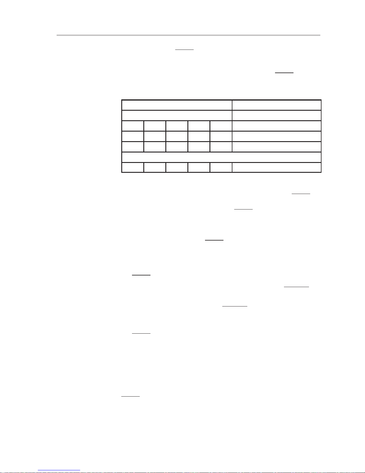
1.3 MSP53C691 Device
The MSP53C691 is optimized to support a four-bit-wide data transfer protocol.
The MSP53C691 has two status bits and three control bits which control the
communication protocol between the master and the slave. The MSP53C691
also has one bit (data/command) which differentiates between command or
speech data feeding into the slave.
MSP53C691 Device
The internal oscillator can be controlled with a 1% resistor for low cost,
or a standard 32.768-kHz crystal for higher precision.
The MSP53C691 also supports the 8-bit wide data transfer but support for
commands is disabled. Switching between 4-bit mode or 8-bit mode is permitted between speech data files.
MSP53C691
(4-bit mode)
Number of data lines 4 8
Number of control lines 3 (strobe, R/W, data/command) 2 (strobe, R/W)
Number of status lines 2 (INRDY, OUTRDY) 2 (INRDY, OUTRDY)
Number of general-purpose I/O lines 4 4
Support for commands (while speaking) Yes No
MSP53C691
(8-bit mode)
Introduction
1-3
Page 10

Pin Assignments and Description
1.4 Pin Assignments and Description
Figure 1–1 shows the pin assignments for the MSP53C691. Table 1–1 provides pin functional descriptions.
Figure 1–1.MSP53C691 Pin Assignments
MSP53C691
PM PACKAGE
(TOP VIEW)
SS
NCNCNCNCNCNCNC
V
NC
NC
NC
NC
NC
NC
NC
V
SS
V
DD
V
DD
R/W
STROBE
OUTRDY
INRDY
TEST
SCANOUT
SYNC
SCANCLK
SCANIN
RESET
PLL
OSCIN
OSCOUT
V
SS
NOTE: Pin 35 is DATA4 in 8-bit mode, or DATA/COMMAND in 4-bit mode.
NC – No internal connection
63 62 61 60 5964 58
1
2
3
4
5
6
7
8
9
10
11
12
13
14
15
16
1718 19
NC
NC
20
NC
21 22 23 24
NCNCNCNCNC
56 55 5457
25 26 27 28 29
NCNCNC
NC
53 52
51 50 49
30 31 32
NC
NC
V
DD
V
48
SS
DACP
47
V
46
DD
DACM
45
V
44
DD
PD4
43
PD5
42
PD6
41
PD7
40
DATA0
39
DATA1
38
37
DATA2
36
DATA3
35
DATA/COMMAND (DATA4)
34
DATA5
33
DATA6
DATA7
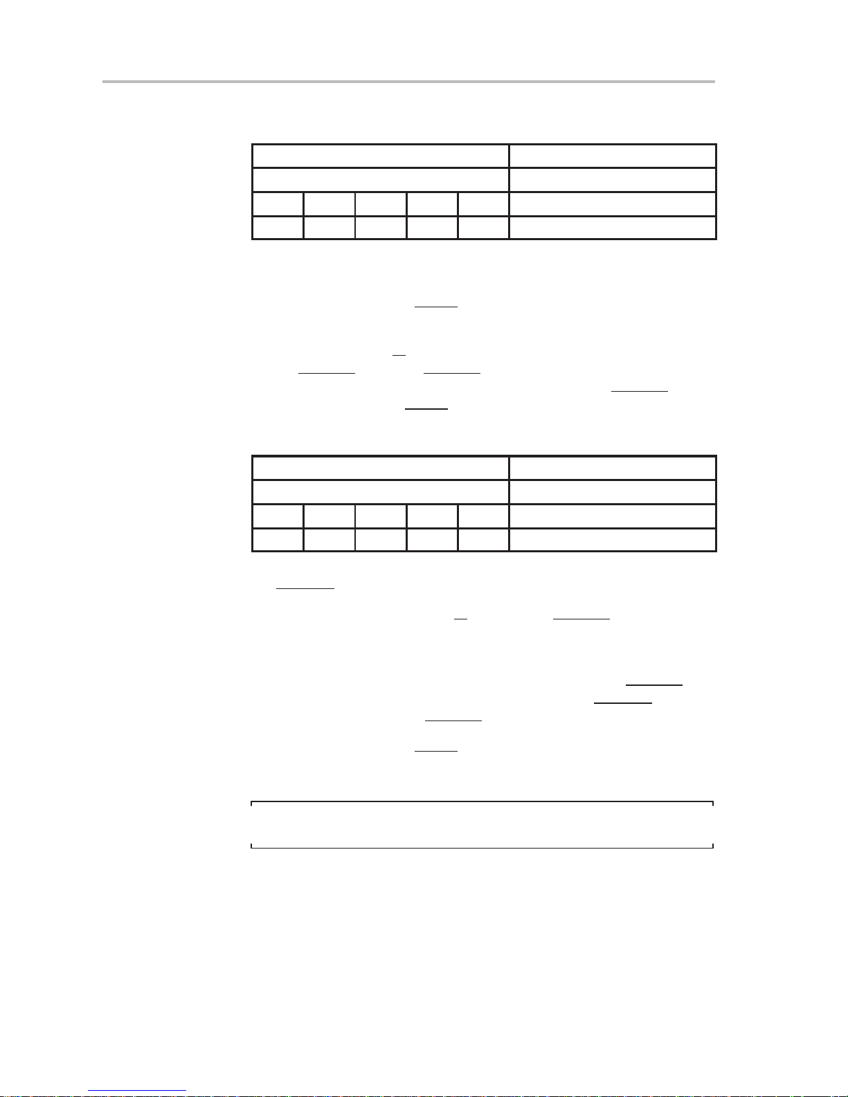
Table 1–1.MSP53C691 Signal Description
NAME
PIN
NO.
INRDY 6 6 O An output signal from the slave to the microcontroller. A low signal
OUTRDY 5 5 O An output signal from the slave to the microcontroller. A low signal
STROBE 4 4 I An input signal to the slave from the microcontroller. STROBE
R/W 3 3 I An input signal to the slave from the microcontroller. Read/write
1-4
PAD
NO.
I/O DESCRIPTION
indicates that the MSP53C691 is ready to accept data or
command. A high signal indicates that the MSP53C691 is busy
and the microcontroller must not write any data or command to it.
indicates that the MSP53C691 is ready to send data or command
to the microcontroller.
sequences read or write operations in conjunction with the R/W
signal. This signal is pulsed high-low-high for read or write
operations sequencing.
select signal which is set high for read operations or set low for
write operations by the microcontroller.
Page 11

Table 1–1. MSP53C691 Signal Description (Continued)
Pin Assignments and Description
NAME
PIN
NO.
PAD
NO.
I/O DESCRIPTION
DATA0–DATA3 39–36 25–22 I/O Data bits 0 through 3 (in 4-bit or 8-bit mode)
DATA4 or
DATA/COMMAND
35 21 I/O Data bit 4 (in 8-bit mode)
Data/command control bit (in 4-bit mode). Low signal indicates
command and high signal indicates data.
DATA5–DATA7 34–32 20–18 I/O Data bits 5 through 7 (8-bit mode only)
Not used (4-bit mode only)
PD4–PD7 43–40 29–26 I/O General-purpose I/O bus
Oscillator Reference Signals
OSCOUT 15 15 O Output of resistor/crystal oscillator
OSCIN 14 14 I Input to resistor/crystal oscillator
PLL 13 13 O Output of phase-lock-loop filter
Scan Port Control Signals‡
SCANIN 11 11 I Scan port data input
SCANOUT 8 8 O Scan port data output
SCANCLK 10 10 I Scan port clock
SYNC 9 9 I Scan port synchronization
TEST 7 7 I C604: test modes
‡NOTE: All these pins must be N.C.
DAC Sound Output
DACP 47 33 O Digital-to-analog output 1 (+) that provides direct speaker drive
capability
DACM 45 31 O Digital-to-analog output 2 (–) that provides direct speaker drive
capability
Initialization
RESET 12 12 I Device initialization
Power Signals
V
DD
V
SS
†
Marked pins are VDD and VSS connections which service the DAC circuitry. These pins tend to sustain a higher current draw .
A dedicated decoupling capacitor across these pins is therefore required.
1, 2, 31,
44, 46
16, 48,
†
49
, 64
†
1, 2, 17,
30, 32
16, 34†,
35, 36
— Processor power, +5 V nominal supply voltage
†
— Ground pin
†
Introduction
1-5
Page 12

DAC Information
1.5 DAC Information
A two-pin push pull that can directly drive a 32-Ω speaker is used in the
MSP53C691. Refer to the
literature number SPSU014, for more information on the D/A and amplifier
circuit.
1.6 Algorithms Supported
-
MELP: Data rates range from 1 kbps to ~ 3.5 kbps at an 8-kHz sample rate.
-
CELP: Data rates can be selected from 3 kbps to 11.2 kbps at an 8-kHz
sample rate.
-
ADPCM
-
FM: frequency modulation for one-channel musical instrument synthesis
-
Mix mode: one channel FM synthesis with MELP or CELP
MSP50x6x Mixed Signal Processor Users Guide
,
1-6
Page 13

Chapter 2
MSP53C691 Hardware Description
This chapter describes the MSP53C691 hardware, including interface, initialization, and timing.
Topic Page
2.1 MSP53C691 Interface Overview 2-2. . . . . . . . . . . . . . . . . . . . . . . . . . . . . . . .
2.2 Microprocessor Interface Description 2-3. . . . . . . . . . . . . . . . . . . . . . . . . . .
2.3 Read Operation by the Master 2-5. . . . . . . . . . . . . . . . . . . . . . . . . . . . . . . . . .
2.4 Write Operation by the Master 2-6. . . . . . . . . . . . . . . . . . . . . . . . . . . . . . . . . .
2.5 MSP53C691 Device Initialization 2-7. . . . . . . . . . . . . . . . . . . . . . . . . . . . . . . .
2.6 Microprocessor Interface Timing 2-8. . . . . . . . . . . . . . . . . . . . . . . . . . . . . . .
MSP53C691 Hardware Description
2-1
Page 14

MSP53C691 Interface Overview
2.1 MSP53C691 Interface Overview
The MSP53C691 interfaces with the master microcontroller either in 4-bit or
in 8-bit mode.
The MSP53C691 and the master microcontroller transfer data across four
(DA TA0–DATA3) or eight (DATA0–DAT A7) data lines, depending upon which
mode the slave is in.
In either mode the transfer of data is controlled by the two control lines: R/W
and STROBE. When the MSP53C691 is ready to receive data from the
microcontroller, it sets INRDY low. The microcontroller sends data to the
MSP53C691 by setting R/W low and then pulsing STROBE high-low-high. The
MSP53C691 latches the data at the rising edge of the STROBE pulse. The
MSP53C691 also sets INRDY high at the rising edge of the STROBE pulse.
Setting INRDY
more data.
When the MSP53C691 is ready to send data to the microcontroller, the
MSP53C691 sets OUTRDY low . The microcontroller responds by setting R/W
high and then pulsing STROBE high-low-high. (The microcontroller latches
the data while STROBE is low.) This informs the slave that the data has been
written to the microcontroller. The MSP53C691 sets OUTRDY high at the rising edge of the STROBE pulse. Setting OUTRDY high indicates that the
MSP53C691 does not have data ready to send.
high indicates that the MSP53C691 is not ready to receive any
Both 4-bit and 8-bit modes are controlled by commands sent to the slave. A
separate bit (DA TA 4) is used in 4-bit mode to differentiate between the speech
data or command sent to the slave. This line is referred to as data/command
line. This is discussed in detail in the software overview section.
2-2
Page 15

2.2 Microprocessor Interface Description
As mentioned in section 2.1, the MSP53C691 interfaces with the master microcontroller either in 4-bit or in 8-bit mode.
2.2.1 4-Bit Mode
The interface between the microcontroller and the MSP53C691 consists of
four control lines, two status lines, and four data lines.
The control lines are:
-
STROBE
-
R/W
-
DATA/COMMAND
-
RESET
The status lines are:
-
INRDY
-
OUTRDY
The speech data or command is transferred on lines:
Microprocessor Interface Description
-
DATA0 through DATA3
Figure 2–1 shows the interfacing diagram.
Figure 2–1.MSP53C691 Interfacing Diagram—4-Bit Mode
V
V
DD
100 kΩ
each
Master MSP53C691
DATA(0–3) DATA(0–3)
Note: STROBE: Active low strobe signal from microcontroller
R/W
RESET
DATA0–DATA3 Data bits 0 through 3
PD4–PD7 General-purpose I/O bus
DACP Output to speaker/amplifier
DACM Output to speaker/amplifier
DATA/COMMAND This bit determines if the data sent by the
100 kΩ
4
Read/write signal from microcontroller
Active low reset signal from microcontroller
microcontroller is data or command.
DD
4.7 kΩ4.7 kΩ
4.7 kΩ
INRDY
OUTRDY
R/W
STROBE
DATA/COMMAND
RESET
MSP53C691 Hardware Description
2-3
Page 16

Microprocessor Interface Description
2.2.2 8-Bit Mode
The interface between the microcontroller and the MSP53C691 consists of
three control lines, two status lines, and eight data lines.
The control lines are:
-
STROBE
-
R/W
-
RESET
The status lines are:
-
INRDY
-
OUTRDY
The data/command lines are:
-
DATA0 through DATA7
Figure 2–2 shows the interfacing diagram.
Figure 2–2.MSP53C691 Interfacing Diagram—8-Bit Mode
V
DD
V
DD
100 kΩ
each
Master MSP53C691
DATA (0–7) DATA (0–7)
Note: STROBE: Active low strobe signal from microcontroller
R/W
: Read/write signal from microcontroller
RESET
INRDY
: Active low indicates that the MSP53C691 is ready to accept data.
OUTRDY
DATA0–DATA7 Data bits 0 through 7
PD4–PD7 General-purpose I/O bus
DACP Output to speaker/amplifier
DACM Output to speaker/amplifier
: Active low indicates that the MSP53C691 is ready to send data.
8
Active low reset signal from microcontroller
4.7 kΩ4.7 kΩ
4.7 kΩ
INRDY
OUTRDY
R/W
STROBE
RESET
2-4
Page 17

2.3 Read Operation by the Master
The process for the read operation by the master is the same in 4-bit and 8-bit
modes. The read operation by the master happens when the slave wants to
send something to the master. The slave initiates the read process by pulling
OUTRDY low when the slave is ready.
The following events take place during the read operation:
1) The MSP53C691 puts the data to be sent to the master on the internal bus.
2) The MSP53C691 sets OUTRDY low to indicate that it is ready to send data
to the microcontroller.
Read Operation by the Master
3) The microcontroller sets R/W
4) The microcontroller sets STROBE low. The data is available on the external data-bus at this point.
5) The microcontroller reads the data from the bus.
6) The microcontroller sets STROBE high. The MSP53C691 also pulls
OUTRDY
high at the rising edge of STROBE.
7) The data is taken off from the external data-bus after STROBE
The microcontroller must latch or read in the data while STROBE is low. When
the microcontroller sets STROBE
to indicate that the data has been successfully transferred.
Figure 2–3 shows the sequence of events of the read operation.
Figure 2–3.Data Transfer—Read
a) Sequence of events for a single read operation:
OUTRDY
R/W
high to indicate a read operation.
goes high.
high, the MSP53C691 sets OUTRDY high
STROBE
DATA
COMMAND/DATA
b) Read—Two speech data transfer sequences:
OUTRDY
R/W
STROBE
DATA
COMMAND/DATA
MSP53C691 Hardware Description
2-5
Page 18

Write Operation by the Master
2.4 Write Operation by the Master
The process for the write operation by the master is the same in 4-bit and 8-bit
modes. The write operation by the master happens when the slave is ready
to request data or command from the master. The slave initiates the write process by pulling INRDY
The following events take place during the write operation:
low when the slave is ready to receive data.
1) The MSP53C691 sets INRDY
from the microcontroller.
2) The microcontroller sets R/W low to indicate a write operation.
3) The microcontroller puts the data in the external data-bus.
4) The microcontroller sets STROBE low after the data is valid.
5) The microcontroller sets STROBE high after a minimum of 300 ns. The
MSP53C691 also pulls INRDY high at the rising edge of STROBE.
6) The data is latched in the MSP53C691 at the rising edge of STROBE.
When the microcontroller sets STROBE
high to indicate that the MSP53C691 is not ready to receive any more data.
Figure 2–4.Data Transfer—Write
a) Sequence of events for a single write operation
R/W
STROBE
INRDY
low to indicate that it is ready to receive data
high, the MSP53C691 sets INRDY
COMMAND/DATA
b) Write—Two speech data transfer sequences
STROBE
COMMAND/DATA
2-6
DATA
R/W
INRDY
DATA
Page 19

2.5 MSP53C691 Device Initialization
The RESET pin is configured as an external interrupt (see Figure 2–5). It
provides the means for hardware initialization of the device. When the RESET
pin is held low, the device assumes a deep sleep state and various registers
are initialized. After the RESET pin is taken high, the device gets initialized and
pulls INRDY low when the slave is ready to receive the oscillator selection
command (see the
oscillator selection command). The oscillator selection command (0xB) is sent
through the DATA0–3 line while setting the DATA4 line low (indicating that it
is a command). When the slave receives the oscillator selection command
(0xB), it pulls INRDY low again to request the parameter (0x1 or 0x2) for the
command. After the parameter is received by the slave, it goes through the rest
of the initialization process and pulls INRDY
stabilized and the slave is ready to receive data/command.
Note:
If the slave does not receive the oscillator selection command as the first
command when INRDY goes low for the first time, or if the slave does not
receive the subsequent parameters for the oscillator control command (0x1
or 0x2), the slave resets itself again.
Software Description
MSP53C691 Device Initialization
chapter for a description of the
low when the oscillator is
Figure 2–5.MSP53C691 RESET Diagram
MSP53C691
RESET
The MSP53C691 is considered to be properly initialized after the following
events take place:
1) The microcontroller sets RESET
2) The microcontroller sets STROBE high throughout the initialization process.
3) The microcontroller sets RESET high.
4) The microcontroller waits for INRDY
5) The microcontroller sets R/W low.
1 kΩ
V
DD
100 kΩ
low.
to go low.
1 µF
6) The microcontroller puts 0xB (oscillator control command) on the data-bus
7) The microcontroller pulls STROBE low, waits for a minimum of 300 ns,
(DATA0–3) and sets the DATA4 (DATA/COMMAND) line low.
then pulls STROBE
high again.
MSP53C691 Hardware Description
2-7
Page 20

Microprocessor Interface Timing
8) The slave latches the command on the rising edge of STROBE.
9) The slave pulls INRDY low again to request the parameter for the oscillator
control command.
10) The master sets R/W low.
11) The master puts the command parameter for the oscillator control command (0x1 or 0x2, see Table 3–1 for details) on the data-bus
(DATA0–DATA3) and sets the DATA4 (DATA/COMMAND) line low.
12) The microcontroller pulls STROBE low, waits for a minimum of 300 ns,
then pulls STROBE high again.
13) The slave latches the command parameter on the rising edge of STROBE.
14) The slave completes the rest of the initialization process and pulls INRDY
low when ready to receive new command. See Figure 2–6 for a timing diagram of the initialization process.
Figure 2–6.Device Initialization
RESET
INRDY
STROBE
R/W
DATA(0–3)
DATA4
2.6 Microprocessor Interface Timing
The MSP53C691 has a self-contained clock generation system. This flexible
clock generation system enables the software to control the clock over a wide
frequency range. The implementation uses a phase-locked-loop (PLL) circuit
that drives the processor clock to a selectable frequency between the
minimum and maximum ranges. Selectable frequencies for the processor
clock are spaced by 65.536 kHz. The PLL clock-reference is also selectable.
between a resistor-trimmed oscillator or a crystal-referenced oscillator, see
Figure 2–2. Internal and periphery clock sources are controlled separately to
provide different levels of power management. Figures 2–3 and 2–4 illustrate
the timing diagram for write and read operations.
B
0×1 or 0×2
2-8
Page 21

Figure 2–7. Oscillator and PLL Connection
a) Crystal Oscillator Operation Connections
MSP50C691
OSCIN OSCOUT PLL
10 Mن
32.768 kHz†
Microprocessor Interface Timing
10 Mن
†
Keep these components as close as possible to the OSCIN, OSC
22 pF†
b) Resistor Trim Operation Connections
MSP50C691
OSCIN OSCOUT PLL
R
(RTO)
†
Keep these components as close as possible to the OSCIN, OSC
470 kΩ 1%†
=
22 pF†
, and PLL pins.
OUT
, and PLL pins.
OUT
C
(PLL)
C
= 3300 pF†
(PLL)
= 3300 pF†
MSP53C691 Hardware Description
2-9
Page 22

2-10
Page 23

Chapter 3
MSP53C691 Software Description
This chapter overviews the software and describes the commands used to
program the MSP53C691.
Topic Page
3.1 Software Overview 3-2. . . . . . . . . . . . . . . . . . . . . . . . . . . . . . . . . . . . . . . . . . . .
3.2 Commands and Data Streams 3-2. . . . . . . . . . . . . . . . . . . . . . . . . . . . . . . . . .
3.3 Sequence of Command Codes and Data Streams 3-3. . . . . . . . . . . . . . . .
3.4 Command Codes 3-5. . . . . . . . . . . . . . . . . . . . . . . . . . . . . . . . . . . . . . . . . . . . .
3.5 Description of the Command Codes 3-8. . . . . . . . . . . . . . . . . . . . . . . . . . . .
MSP53C691 Software Description
3-1
Page 24

Software Overview
3.1 Software Overview
The MSP53C691 is a slave device that is controlled using a formatted
communications sequence that transfers commands and data streams from
the master microcontroller. The commands are combined at the top level into
several main groups (command header). Each main group has sublevels
(level 1 and level 2) that may require several parameters, depending upon the
group.
3.2 Commands and Data Streams
Two types of communications are sent to the MSP53C691: speech data
streams and commands (with parameters). The command headers and the
level 1 and level 2 parameters are always sent to the MSP53C691 a nibble at
a time through data lines DATA0–DATA3. However, the speech data is sent
over the four-bit data lines (DATA0–DATA3) in four-bit mode, while speech
data is sent over the eight-bit data lines (DATA0–7) in eight-bit mode. When
sending speech data in four-bit mode, the DA TA4 (DATA/COMMAND) line is
always pulled high to differentiate speech data from a command. The DA TA4
(DA T A/COMMAND) line is always pulled low while sending commands to the
MSP53C691. In four-bit mode, commands can be sent to the MSP53C691 at
the beginning of a speech file or at any other time while speaking. In eight-bit
mode, commands can only be sent to the MSP53C691 at the beginning of
each speech file. Support for commands while speaking a phrase is not available in eight-bit mode; it is only available after speaking of a phrase is complete.
-
The DA T A/COMMAND line defines what type of information is being sent
(data or command) to the MSP53C691. The command or speech data
sent to the MSP53C691 is distinguished by the following state of the
DATA/COMMAND line.
J
Data = 1
J
Command = 0
-
A data stream or speech data is sent to the MSP53C691 to provide the
data file for speaking.
-
Command codes are sent to the MSP65C691 to control functions such as
speaking start or stop, toggle I/O, volume control, oscillator control, configure internal registers, etc. See Table 3–1 for a complete list of command
codes.
3-2
Page 25

Sequence of Command Codes and Data Streams
Note:
Throughout the rest of the chapter it is assumed that data from the
MSP53C691 is always read four nibbles at a time. The MSP53C691 pulls
OUTRDY low when it wants to send a nibble to the master (read from the
MSP53C691). It is also assumed that the data is sent to the MSP53C691
from the master only when the MSP53C691 pulls INRDY
low. In four-bit
mode, the DA T A4 (DA TA/COMMAND) bit is low when a command or its parameters are written to the MSP53C691, and the DATA4 (DATA/COMMAND) bit is high when the speech or FM data is written to the MSP53C691.
While sending speech or command in four-bit mode, the data is always sent
most-significant nibble first and least-significant nibble last.
All commands and their parameters are sent with a four-bit interface. Commands and their parameters are sent to the slave through data lines
DATA0–DATA3 while DATA4 (DATA/COMMAND) line is set low.
The procedures for reading from or writing to the MSP53C691 are described
in the
Hardware Description
chapter.
3.3 Sequence of Command Codes and Data Streams
The sequence for sending the command codes and data streams is as follows:
-
The sequence for the command codes consists of a command header, a
level 1, and, sometimes, a level 2 parameter. The command header controls the operation performed by the MSP53C691. Level 1 and level 2 are
two levels of command information that further define the command code.
Each nibble of the command code is sent along with a 0 in the DA TA/COMMAND line to indicate that it is a command. Refer to section 3.3.2,
ters
-
3.3.1 Command Header
The command header is the first information of the command code sequence
sent to the MSP53C691. The command header controls the operation being
performed by the MSP53C691. The MSP53C691 recognizes the following
command headers:
and Table 3–1,
Data streams are speech data sent to the MSP53C691 from speech files
processed by the SDS6000 (see Appendix C for details). Each nibble of
the speech data is sent along with a 1 on the DA TA/COMMAND line to indicate that it is speech data.
Command Codes
for additional information.
Parame-
-
-
-
-
-
Command header 1—Configure internal registers
Command header 2—Set/Clear I/O ports PD4 through PD7
Command header 3—Read contents of I/O ports
Command header 4—Start speaking
Command header 5—Stop speaking
MSP53C691 Software Description
3-3
Page 26

Sequence of Command Codes and Data Streams
-
Command header 6—Adjust volume
-
Command header 7—Return status of data buffers
-
Command header 8—Initiate sleep mode
-
Command header 9—Receive FM data (while speaking in FM only or in
mix mode)
-
Command header A—Perform speed/pitch shift
-
Command header B—Set up oscillator
The command headers are sent to the MSP53C691 in four-bit nibbles with a
0 in the DATA4 line in either four-bit or eight-bit mode.
CAUTION
Support for sending commands while speaking is not available in
eight-bit mode. In eight-bit mode, commands can be sent to the slave
between speaking phrases.
3.3.2 Parameters
3.3.3 Return Values
For the command codes, there are two types of parameters that are sent to
the MSP53C691 after sending the command header: level 1 and, if required,
level 2. Level 1 and level 2 are levels of command information that further
defines the command code. For example, if the command header is
Volume
(one nibble command code 0x6), then the level 1 parameter (one
Adjust the
nibble, 0x1 through 0x6) defines what level the volume is being set to (that is,
low, medium, or high). Also, if the command header is
Registers
(one nibble command code 0x1), then the level 1 parameter defines
Configure Internal
which internal register address to write to (two nibbles specifying the address
of the register). The level 2 parameter is the data written to the internal register
(four nibbles specifying the word to be written in the register). All the command
headers and Level 1 and level 2 parameters are sent to the MSP53C691 a
nibble at a time with the DATA4 (DATA/COMMAND) bit set low. While
interleaving commands between speech data, it is advisable to send all the
nibbles of the command (command header, level 1, and level 2 parameters,
if applicable) before sending more speech data or commands. Refer to
Table 3–1,
Command Codes
, for additional information.
The MSP53C691 can return values to the microcontroller when required. The
MSP53C691 sends return values to the master either to respond to a command, to return error codes, or to provide its current status. The values returned vary in content, depending on the command code initiated and on the
status of the MSP53C691. The following is a list of returned values from the
MSP53C691:
3-4
Page 27

Command Codes
Returned Values Description
0x0055 Returned when the MSP53C691 successfully plays a speech file. In mix mode,
0x0055 is returned when the MSP53C691 has finished playing both the FM and
the speech file.
0x0054 Returned in mix mode when the MSP53C691 has successfully finished playing
a speech file and is waiting to start a new file or for the FM to finish playing.
0x0053 Returned in mix mode when the MSP53C691 has successfully finished playing
an FM file and is waiting for the speech file to finish playing.
0x9999
Returned when an error is encountered. This error is returned when either:
• An invalid command header or and invalid level 1 or level 2 parameter is
issued by the master.
• An invalid port address to be written to or to be read from is specified.
• An invalid file format is encountered while playing multiple files In mix mode.
0x1234 Returned when there is an error recognizing the header byte in the speech file
or the stack is overflowed
0x0N23 Returned (in mix mode or while speaking FM only) when the FM buffer becomes
nearly empty and FM data is needed to fill up the FM buffer . N denotes the number of FM bytes needed to fill up the FM buffer.
CAUTION
The MSP53C691 waits until all of the four nibbles have been sent to the
microcontroller. If the microcontroller delays in reading the data from the
MSP53C691, the speech operation can be interrupted. Therefore, the
microcontroller must read the data as soon as the OUTRDY goes low.
3.4 Command Codes
The valid command codes are described in Table 3–1 and paragraph 3.5.
Command codes include the command header (one nibble), level 1
parameters (one or two nibbles), and, sometimes, level 2 (four nibbles)
parameters. As shown in Table 3–1, there are occasions when values are
returned to the slave as a result of the command that is initiated. These return
values are always four nibbles in size and are sent over the DATA0–DATA3
data lines.
In four-bit mode, the commands (command header and level 1 and level 2
parameters) are sent to the MSP53C691 four bits (a nibble) at a time with
DA TA4 set to 0 for every transmitted nibble. In four-bit mode, commands can
be sent while speaking a phrase, but in eight-bit mode commands can only be
sent between speaking phrases. After receiving the command to speak in 8-bit
mode, the slave expects speech data in 8–bits. No other command can be sent
to the slave during speaking. The slave goes to the 4-bit mode to receive
MSP53C691 Software Description
3-5
Page 28

Command Codes
further commands after finishing speaking (either in 4-bit or in 8-bit mode). All
commands require at least one nibble of level 1 parameter. There are some
commands that require more than one nibble of level 1 parameter. Some
commands require more than one nibble of level 2 parameter. Some
commands return four nibbles back to the master in response. For example,
a return buffer status (command code 0x7) followed by a level 1 parameter
(0x1 for non-FM buffer) returns four nibbles reporting the number of bytes left
to fill up the buffer back to the master.
See section 3.5, Description of the Command Codes, for a description of each
command.
Table 3–1.Command Codes
Command
Header
1 N1N
2 N None None Upper four bits for port D
3 N1N
4 1 None None Speak CELP, MELP, or ADPCM in four-bit data transfer
4 2 None None Speak CELP, MELP, or ADPCM in eight-bit data transfer
4 3 None None Test mode
4 4 none None Play FM (Music) in four-bit mode only
4 5 none None Speak mixed mode in four-bit mode only (FM +
4 6 None None Speak multiple phrases in mix mode—see the details
4 7 None None Play sinewave in test mode at 1 kHz
5 1 none None Stop speaking all (in mix or nonmix mode)
5 2 None None Stop speaking CELP/MELP only in mix mode
5 3 None None Stop speaking FM only in mix mode
Note: Each nibble is sent to the master with DATA4 bit set to 0, indicating that it is a command.
N—Represents one nibble.
N1N2N3N4—Represents four nibbles, with N1 being the first nibble sent and N4 being the 4th nibble sent (MSB and LSB).
The numbers in the box represent the actual value of the nibble sent to the MSP53C691.
Parameters
Level 1 Level 2
Port
address
PD4–PD7
Port
address
2
2
V alue to
be written
N1N2N3N
None N1N2N3N
Return
Values
Configure Internal Registers
None Write to internal registers for configuration
4
Set/Clear I/O Ports, PD4 Through PD7
(Note: Configuration of port D4–7 as output is required)
Read Contents of I/O Ports
Value
4
Start Speaking
under the discussion of the command
Stop Speaking
Returns the port value
Description
CELP/MELP)
3-6
Page 29

Command Codes
Table 3–1. Command Codes (Continued)
Adjust the Volume
6 1 none none Level 1 (lowest volume)
6 2 none none Level 2
6 3 none none Level 3
6 4 none none Level 4
6 5 none none Level 5
6 6 none none Level 6 (highest volume)
Command
Header
7 1 None N1N2N3N
7 2 None N1N2N3N4Returns the number of bytes required to fill up the FM
8 1 None None Light sleep (see Table 2–3 of SPSU014)
8 2 None None Mid sleep (see Table 2–3 of SPSU014)
8 3 None None Deep sleep (see Table 2–3 of SPSU014)
9 N None None Receive FM data
A 0 N1N2N3N
A 1 N1N2N3N
A 2 N1N2N3N
A 3 None None Reserved (TI test code)
B 1 None None Crystal mode
B 2 None None Resistor trim mode
Parameters
Level 1 Level 2
Return
Values
Description
Return Status of Data Buffers
Returns the number of bytes required to fill up the
4
CELP/MELP buffer
Initiate Sleep Mode
Wake-up from sleep mode can be performed by putting
dummy data in the bus and pulsing STROBE
Receive FM Data
N = number of FM bytes the master is going to send
Perform Speed/Pitch Shift
None Slow down MELP
4
None Speed up MELP
4
None Pitch shift in MELP
4
Oscillator Control
buffer
Note: Each nibble is sent to the master with DATA4 bit set to 0, indicating that it is a command.
N—Represents one nibble.
N1N2N3N4—Represents four nibbles, with N1 being the first nibble sent and N4 being the 4th nibble sent.
The numbers in the box represent the actual value of the nibble sent to the MSP53C691.
MSP53C691 Software Description
3-7
Page 30

Description of the Command Codes
3.5 Description of the Command Codes
3.5.1
Command Header 1—Configure Internal Registers
This command is used to configure the MSP53C691 internal registers. Certain
values in certain registers are not allowed to be modified (see note at the end
of this section). Attempting to modify these values when writing to those registers has no effect. The command header for configuring internal registers for
the MSP53C691 is one nibble long and of value 1 as shown. This header is
sent across the four data lines. The sequence of events to configure the internal registers is as follows:
1) The MSP53C691 pulls INRDY
2) The master sends the command header 0x1 over the data lines.
Write Operation to Configure Internal Registers
DATA4 DATA3 DATA2 DATA1 DATA0
0 0 0 0 1
3) The MSP53C691 pulls INRDY low again to request level 1 parameters.
The level 1 parameter that defines the address of the internal register is
two nibbles long in this case, see the following examples:
Most significant (first nibble) Least significant ( Second nibble)
X X
low to request a command or data.
Data Lines
4) The master sends the two nibbles back to back in response to the two
consecutive lowerings of INRDY.
Note:
When sending the two nibbles that make up the address of the register, send
the first nibble (most significant) first.
Example 1: To configure pins 7 and 5 of port D as outputs and pins 6 and 4
as inputs, we need to write to the port D control register. The address for the
register to be configured is 0x1C, then the two nibbles (8 bits) are written as
1C:
MSB LSB
7 6 5 4 3 2 1 0
0 0 0 1 1 1 0 0
Perform the following write operation by writing the two nibbles (8 bits) MSB
first, as shown. The two nibbles are written one nibble at a time—in each case
the DATA4 bit is pulled low, indicating that a command is being sent.
3-8
Page 31

Description of the Command Codes
Most Significant
DATA LINES
DATA4 DATA3 DATA2 DATA1 DATA0
0 0 0 0 1 Firstst nibble sent
Least Significant
0 1 1 0 0 Second nibble sent
5) After the level 1 parameters are received, the MSP53C691 pulls INRDY
low again requesting the data to be written to the registers. The data is 16
bits long and is transferred to the MSP53C691 a nibble at a time (most-significant nibble first). The master must send four nibbles (for 16-bit data)
back to back in response to four consecutive lowerings of INRDY
.
Note:
The data to be written to the configuration registers is always 16 bits long.
If there are less than 16 bits to be written to the registers, then there should
be leading zeroes to make it 16 bits long.
Example 2: The value to be written to the internal register is 0xA0, then the
four nibbles (16 bits) are written as 0x00A0:
MSB LSB
15 14 13 12 11 10 9 8 7 6 5 4 3 2 1 0
0 0 0 0 0 0 0 0 1 0 1 0 0 0 0 0
Perform the following write operation by writing the four nibbles (16 bits) MSB
first, as shown. The four nibbles are written one nibble at a time with the DA TA4
line set to 0, indicating that a command parameter is being sent.
Most Significant
DATA LINES
DATA4 DATA3 DATA2 DATA1 DATA0
0 0 0 0 0 First nibble sent
0 0 0 0 0 Second nibble sent
0 1 0 1 0 Third nibble sent
Least Significant
0 0 0 0 0 Fourth nibble sent
NOTE:
-
Do not write to the following addresses:
J
Port A
H
Data, address 0x00
H
Control, address 0x04
MSP53C691 Software Description
3-9
Page 32

Description of the Command Codes
J
J
J
J
J
J
Port B
H
Data, address 0x08
H
Control, address 0x0C
Port C
H
Data, address 0x10
H
Control, address 0x14
Port D (PD0 – PD3)
H
Data, address 0x18
H
Control, address 0x1C
Port E
H
Data, address 0x20
H
Control, address 0x24
Port F
H
Data, address 0x28
Port G
H
Data, address 0x2C
J
Timer 1 period and countdown register, address 0x3A and 0x3B
J
Timer 2 period and countdown register, address 0x3E and 0x3F
Note: Refer to Table 2–2 in SPSU014 for a complete listing of the port
addresses.
3.5.2 Command Header 2—Set/Clear I/O Ports, PD4 Through PD7
This command can be used to pull a general-purpose I/O pin low or high. The
PD4–7 pins are defined as general-purpose I/O pins in the MSP53C691.
Before sending the command, it is necessary to configure the port pins to the
appropriate state (INPUT or OUTPUT) by configuring the internal control
registers. This command causes the following sequence of events:
1) The MSP53C691 pulls INRDY
master sends the command header 0x2 for toggling I/O ports PD4 through
PD7 of the MSP53C691 as shown in the following table:
WRITE OPERATION TO TOGGLE I/O PORTS
DATA4 DATA3 DATA2 DATA1 DATA0
0 0 0 1 0
low requesting command or data. The
DATA LINES
2) The MSP53C691 pulls INRDY low again to receive the level 1 parameter.
The level 1 parameter for this command is only one nibble long and is
effectively written to the upper four bits of the port (PD4–PD7). This onenibble parameter defines which pins are being toggled (see examples
below).
3-10
Page 33

Example 1: If PD5 is toggled high, then the one nibble level 1 parameter is
written as 0010; this sets PD5 high.
PINS
PD7 PD6 PD5 PD4
0 0 1 0
Example 2: If none of the pins are toggled high, then the one nibble parameter
is written as 0000; this sets PD4 through PD7 low.
PINS
PD7 PD6 PD5 PD4
0 0 0 0
Note:
Port D must be set as output mode first with the configure register command
for the toggle I/O command to work properly.
3.5.3 Command Header 3—Read Contents of I/O Ports
This command can be used to read back the contents of a port. The command
header for this command is one nibble long and the level 1 parameter
specifying the address of the port to be read is two nibbles long. This command
causes the following sequence of events:
Description of the Command Codes
1) The MSP53C691 pulls INRDY
low to request a command or data.
2) The master sends the command header 0x3 to read the port as follows:
WRITE OPERATION FOR READ CONTENTS OF I/O PORTS
DATA LINES
DATA4 DATA3 DATA2 DATA1 DATA0
0 0 0 1 1
3) The MSP53C691 pulls INRDY low again to receive the level 1 parameters.
The level 1 parameter is two nibbles long and defines the address of the
port, see the following example:
Most significant ( first nibble) Least Significant ( second nibble)
X X
4) The master sends the two nibbles in response to the two consecutive lowerings of INRDY.
Note:
When sending the two nibbles, send first nibble (most-significant nibble) first.
Example 1: To read port D pins 7–4, we need to read the port D data register.
The address for the port to be read is 0x18, then the two nibbles (8 bits) are
written as 0x18:
MSP53C691 Software Description
3-11
Page 34

Description of the Command Codes
MSB
7 6 5 4 3 2 1 0
0 0 0 1 1 0 0 0
LSB
Perform the following write operation by writing the two nibbles (8 bits) MSB
first, as shown. The two nibbles are written one nibble at a time with the DA TA4
line pulled low in each case, indicating that a command is being sent.
Most Significant
DATA LINES
DATA4 DATA3 DATA2 DATA1 DATA0
0 0 0 0 1 First nibble sent
Least Significant
0 1 0 0 0 Second nibble sent
5) After the command header and all the parameters are received, the command is executed by setting OUTRDY
low and the four nibbles of data contained in the port register are sent (MSB first, LSB last) to the microcontroller.
6) After receiving the level 1 command parameter (port address), the
MSP53C691 pulls OUTRDY low four times to return the contents of the
port to the master. Each lowering of OUTRDY transfers a nibble
(DA TA0–DA T A3) to the master—the first being the most-significant nibble.
CAUTION
The MSP53C691 waits until all of the four nibbles have been sent to the
microcontroller. If the microcontroller delays in reading the data from the
MSP53C691, the speech operation can be interrupted. Therefore, the
microcontroller must read the data as soon as the OUTRDY goes low.
7) The MSP53C691 pulls INRDY low again to request new data or command.
Note: The contents of the following port addresses can be read:
-
Port A
J
Data register (address 0x00)
J
Control register (address 0x04)
3-12
Page 35

-
FUNCTIONS
Port C
J
Data register (address 0x10)
J
Control register (address 0x14)
-
Port D
J
Data register (address 0x18)
J
Control register (address 0x1C)
-
DAC
J
Data register (address 0x30)
J
Control register (address 0x34)
-
IntGenCtrl register (address 0x38)
-
Interrupt flag register (address 0x39)
Note: Refer to Table 2–2 in SPSU014 for a complete listing of the port
addresses.
3.5.4 Command Header 4—Start Speaking
This command is used to command the MSP53C691 to start speaking. This
command has several level 1 parameters to describe the mode in which the
MSP53C691 speaks. The command header is one nibble long and is written
0100 as shown in the following table. The DA TA4 bit is low while sending this
nibble.
Description of the Command Codes
WRITE OPERATION FOR START SPEAKING
DATA LINES
DATA4 DATA3 DATA2 DATA1 DATA0
0 0 1 0 0
The command header 0100 is followed by a level 1 parameter that is one
nibble long and instructs the MSP53C691 to perform the functions defined in
the following table:
DATA LINES
DATA4 DATA3 DATA2 DATA1 DATA0
0 0 0 0 1 Speak CELP, MELP, or ADPCM in
four-bit data transfer mode
0 0 0 1 0 Speak CELP, MELP, or ADPCM in
eight-bit data transfer mode
0 0 0 1 1 Test mode (nibble in = nibble out)
0 0 1 0 0 Play FM (music) in four-bit data
transfer mode
0 0 1 0 1 Speak mixed mode in four-bit data
transfer mode (FM + CELP/MELP)
0 0 1 1 0 Speak multiple files in mix mode
MSP53C691 Software Description
3-13
Page 36

Description of the Command Codes
The different modes of speaking are described in detail in the following
subsections.
3.5.4.1 Speaking CELP, MELP, ADPCM in Four-Bit Data Transfer Mode
Commands and data are sent over a four-bit interface. When data is sent over
the DATA0 through DATA3 lines, DATA4 (pin 35) becomes the
DATA/COMMAND control line. The DATA/COMMAND line defines whether
the information on DA TA0 through DA T A3 is data or commands. When DA T A0
through DATA3 and DATA/COMMAND bits are received, the MSP53C691
analyzes the DATA/COMMAND bit to determine if the information is data or
commands being received on DATA0 through DATA3 lines.
DATA/COMMAND LINE DESCRIPTION
Set to 0 Command sent to the MSP53C691
Set to 1 Data sent to the MSP53C691
The following typical sequence of events takes place while playing CELP,
MELP, or ADPCM in four-bit mode:
1) The MSP53C691 pulls INRDY low and waits for a command from the
master.
2) The master sends the command header 0x4 (command header for speaking in four-bit mode) on the data bus. Note that writing 0x04 to the data bus
ensures that the DATA4 line is low, indicating that value on data lines
DATA0–DATA3 is a command.
Most Significant
DATA LINES
DATA4 DATA3 DATA2 DATA1 DATA0
0 0 1 0 0 First command header sent
3) After receiving the header, the MSP53C691 pulls INRDY low again and
waits for the level 1 parameter from the master.
4) The master sends the level 1 command parameter 1 to indicate the four-bit
transfer mode for CELP, MELP, or ADPCM.
Most Significant
DATA LINES
DATA4 DATA3 DATA2 DATA1 DATA0
0 0 0 0 1 Level 1 parameter sent
5) The MSP53C691 interprets the command and initializes itself to get ready
to speak.
6) The MSP53C691 pulls INRDY low, indicating that it is ready to receive
more commands or speech data.
3-14
Page 37
Description of the Command Codes
7) The master can now start sending speech data from a file in response to
each lowering of INRDY . Note that, while sending speech data, the DA T A4
line must be high, indicating that speech data is being sent. For example,
to send the speech data byte 0x24 to the MSP53C691, the master must
put 0x12 on the data bus in response to the lowering of INRDY
. When the
MSP53C691 is again ready to receive the next nibble, the master puts
0x14 on the data bus again.
Most Significant
DATA LINES
DATA4 DATA3 DATA2 DATA1 DATA0
1 X X X X First nibble sent
1 X X X X Second through X nibble sent
Least Significant
1 X X X X Last nibble sent
8) The master can send a command (such as volume control)-between the
speech data while sending speech data. In this case the master first sends
the command header nibble of the command in response to INRDY low
and then sends the required level 1 and/or level 2 parameter nibbles in response to each consecutive lowering of INRDY
. Note that the master must
ensure that the DA TA4 line is also low , indicating that the value in data lines
DATA0–DATA3 is a command. If the master starts sending a command,
then it must send all the parameters of the command back to back in response to each lowering of INRDY before reverting back to sending the
rest of the speech file data again.
9) After sending the last nibble of speech data, the master can send dummy
data (0xFF) to the slave in response to each consecutive lowering of
INRDY until the slave detects the end-of-speech data.
10) When the MSP53C691 detects the end-of-speech, it pulls OUTRDY low.
1 1) The master must then read the data from the bus. Note that only the lower
four bits of the bus are valid data. OUTRDY goes low three more times,
sending a total of four nibbles (0, 0, 5, and 5) if speaking of the phrase was
successful.
12) INRDY goes low again, indicating that the MSP53C691 is ready to receive
a new command.
3.5.4.2 Speaking CELP, MELP, ADPCM in 8-Bit Data Transfer Mode
Data is sent over an eight-bit interface (DA T A0–DAT A7). Sending commands
while speaking is not supported in this mode. When the speaking of a phrase
is finished, the master can again send any command over the DA T A0–DA T A3
lines along with pulling DATA4 line low in response to the next lowering of
. In other words, the MSP53C691 goes back to the four-bit mode after
INRDY
it finishes speaking a phrase in eight-bit mode. The master must send the
command header (4) and level 1 parameter (2) to speak a phrase again in
eight-bit mode.
MSP53C691 Software Description
3-15
Page 38

Description of the Command Codes
While sending a command in between phrases, the master must make sure
that the DATA4 bit is low.
The following is a typical sequence of events that takes place while playing
CELP, MELP, or ADPCM in eight-bit mode:
1) The MSP53C691 pulls INRDY
low and waits for a command from the
master.
2) The master sends the command header 0x04 to the MSP53C691. Note
that writing 0x04 on the data bus ensures that the DA TA4 line is also low,
indicating that the value on data lines DATA0–DATA3 is a command.
Most Significant
DATA LINES
DATA4 DATA3 DATA2 DATA1 DATA0
0 0 0 1 0 First command header sent
3) After receiving the command header, the MSP53C691 again pulls INRDY
low and waits for the level 1 parameter from the master.
4) The master sends 0x2 as the level 1 parameter to indicate the eight-bit
transfer mode for CELP, MELP, or ADPCM as follows:
Most Significant
DATA LINES
DATA4 DATA3 DATA2 DATA1 DATA0
0 0 0 1 0 Level 1 parameter sent
5) The MSP53C691 interprets the command and initializes itself to get ready
to speak.
6) The MSP53C691 pulls INRDY low, indicating that it is ready to receive
speech data.
7) The master can now start sending speech data from a file in response to
each lowering of INRDY over the whole eight-bit data bus (DA TA0 through
DA TA7).
Most Significant
DATA LINES
DATA7 DATA6 DATA5 DATA4 DATA3 DATA2 DATA1 DATA0
X X X X X X X X First byte sent
8) The master can not send a command while sending speech data in eightbit mode. The master has to send the speech data in response to each
lowering of INRDY
by putting eight-bit speech data on the bus.
9) After finishing sending the last byte of speech data, the master can send
dummy data (0xFF) to the slave to respond to each consecutive lowering
of INRDY
until the slave detects the end-of-speech.
3-16
Page 39

Description of the Command Codes
10) When the MSP53C691 detects the end-of-speech, it pulls OUTRDY low.
1 1) The master then must read the data from the bus. Note that only the lower
four bits of the bus are valid data. OUTRDY goes low three more times after that, sending a total of four nibbles (0, 0, 5, and 5) if the speaking of the
phrase was successful.
3.5.4.3 Test Mode
12) INRDY
goes low, indicating that the MSP53C691 is ready to receive a new
command. At this point the slave changes back to four-bit mode. Now the
master can send any command to the slave on the four-bit data bus
(DA T A0–DA T A3) with the DA T A4 line pulled low . If the master must speak
again in eight-bit mode, repeat Steps 1 through 12.
Note:
The eight-bit interface is recommended for ADPCM.
The eight-bit interface does not support any interleaved commands (STOP,
volume control, etc.). Hold RESET low to stop speaking in the middle of a
phrase.
A header byte is embedded in the speech data to indicate which algorithm
(MELP, CELP, etc.) to speak. When a certain mode of data transfer is selected (four-bit or eight-bit), the first few bytes of the speech file set up the
MSP53C691 to play the speech file at the proper speed for the synthesizer
algorithm. After the speech file is finished, the MSP53C691 goes back to running at 8 MIPS.
If the test mode is selected, data is transferred to and from the MSP53C691
(one nibble at a time). The MSP53C691 device receives one nibble of data and
then sets OUTRDY low, meaning that the MSP53C691 is ready to send data.
The MSP53C691 then sends the same nibble of data back to the
microcontroller. INRDY is then set low , meaning that the MSP53C691 is ready
to receive more data.
The following is a typical sequence of events for the test mode:
1) The MSP53C691 pulls INRDY
2) The master sends the command header 0x4 on the data bus. Note that
3) After receiving the header, the MSP53C691 pulls INRDY low again and
low and waits for a command from the
master.
writing 0x4 to the data bus ensures that the DA TA4 line is low, indicating
that the value on data lines DATA0–DATA3 is a command.
Most Significant
DATA LINES
DATA4 DATA3 DATA2 DATA1 DATA0
0 0 1 0 0 First command header sent
waits for a level 1 parameter from the master.
MSP53C691 Software Description
3-17
Page 40
Description of the Command Codes
4) The master sends 0x03 to the MSP53C691 as the level 1 parameter to indicate the test mode.
DATA4 DATA3 DATA2 DATA1 DATA0
0 0 0 1 1 Level 1 parameter sent
5) The MSP53C691 interprets the command and initializes itself to get ready
to go to the test mode.
6) The MSP53C691 pulls INRDY low, indicating that it is ready to receive test
data.
7) The master pulls R/W low, puts a nibble of test data on the bus, and pulses
the STROBE. When the STROBE is pulled low and then back to high, the
data is latched into the MSP53C691 at the rising edge of STROBE
MSP53C691 pulls INRDY high. Note that the data is sent on
DATA0–DATA3 lines only.
Most Significant
DATA LINES
and the
Most Significant
DATA LINES
DATA4 DATA3 DATA2 DATA1 DATA0
X X X X X First nibble sent
8) When the data is latched into the MSP53C691, the MSP53C691 pulls
OUTRDY low.
9) The master then must pull R/W high and pull STROBE low.
10) The master then must read the data from data lines DAT A4–DA TA7. Note
that only the upper four bits of the bus (DATA4–DATA7) are valid data
echoed back to the master. After that the master must pull STROBE high,
indicating that the data has been read from the bus. OUTRDY goes high
at the rising edge of the STROBE
1 1) The MSP53C691 pulls INRDY
.
low again for the next data and the process
repeats.
Note:
The only way to get out of the test mode is to reset the device.
3-18
Page 41

Description of the Command Codes
3.5.4.4 Playing Single Channel FM Synthesis in Four-Bit Transfer Mode
The MSP53C691 can play single-channel FM in four-bit transfer mode.
Sending commands to perform other functions (volume control, toggle I/O,
etc.) is also supported in this mode. The FM data is supplied to the
MSP53C691 from the master over the four-bit data lines (DA TA0–DA T A3). The
DATA/COMMAND line is pulled high while transferring FM data. The
MSP53C691 sends a request back to the master (by pulling OUTRDY
transferring four nibbles to the master) whenever it needs more FM data. The
master then must send a command back to the MSP53C691 informing how
many bytes of FM data are going to be sent. Then the master can send the
promised number of bytes to the MSP53C691 in response to each lowering
of INRDY
. The following is a typical sequence of events for FM transfer:
1) The MSP53C691 pulls INRDY low and waits for a command from the master.
2) The master sends the command header 0x04 to the MSP53C691. Note
that writing 0x04 to the data bus ensures that the DA TA4 line is low , indicating that the value on data lines DATA0–DATA3 is a command.
Most Significant
low and
DATA LINES
DATA4 DATA3 DATA2 DATA1 DATA0
0 0 1 0 0 First command header sent
3) After receiving the header, the MSP53C691 pulls INRDY low to expect the
level 1 parameter from the master.
4) The master sends 0x4 as the level 1 parameter to indicate four-bit transfer
mode for playing FM.
Most Significant
DATA LINES
DATA4 DATA3 DATA2 DATA1 DATA0
0 0 1 0 0 Level 1 parameter sent
5) The MSP53C691 interprets the command and initializes itself to get ready
to speak FM.
6) The MSP53C691 pulls OUTRDY low, indicating that it must send a nibble
back to the master.
7) The master reads the data from the bus (DATA0–DATA3).The
MSP53C691 pulls OUTRDY low three more times to send a total of four
nibbles. The four nibbles sent to the master are 1, 8, 2, and 3 respectively .
The 1 and 8 are interpreted as 18H (24 decimal) bytes needed to fill up the
FM buffer initially . The 2 and 3 are interpreted as 23, characterizing the FM
data request to the master.
MSP53C691 Software Description
3-19
Page 42

Description of the Command Codes
DATA3 DATA2 DATA1 DATA0
0 0 0 1 First nibble sent
1 0 0 0 Second nibble sent
0 0 1 0 Third nibble sent
Least Significant
0 0 1 1 Fourth nibble sent
8) The MSP53C691 then pulls INRDY low to indicate that it is ready to receive FM data.
9) The master can now start sending FM data from a file in response to each
lowering of INRDY. Note that while sending speech FM, the DATA4 line
should be high indicating that FM data is being sent. For instance, to send
the FM data byte 0x38 to the MSP53C691, the master must put 0x13 on
the data bus in response to lowering of INRDY
again ready to receive the next nibble, the master puts 0x18 on the data
bus.
Most Significant
DATA LINES
. When the MSP53C691 is
Most Significant
DATA LINES
DATA4 DATA3 DATA2 DATA1 DATA0
1 X X X X First nibble sent
1 X X X X Second through X nibbles sent
Least Significant
1 X X X X Last (24X2=48th) nibble sent
Note:
It is very important to note that the master must send the exact number of FM
data bytes initially requested by the MSP53C691 while filling up the buffer.
If the master has finished sending the exact number of FM data bytes as
requested by the MSP53C691 to initially fill up the buffer and the
MSP53C691 has pulled INRDY
low to request more data or command, the
master can either send a command to perform any task (volume control,
toggle I/O, etc.) or send a dummy command (0x00) if it does not want to send
a valid command.
10) The MSP53C691 starts playing FM after the buffer is filled (that is, the first
24 (decimal) bytes from the file have been received). The MSP53C691
continues to pull INRDY low and waits for a command from the master.
The master can either send a valid command to fulfill the request, or a
dummy command if it doesn’t have any more commands to send.
3-20
Page 43

Description of the Command Codes
1 1) When the MSP53C691 needs more FM data, it pulls OUTRDY low to send
a nibble back to the master. The master must read the nibble from the bus.
The MSP53C691 pulls OUTRDY low three more times to transfer a total
of four nibbles to the master. The four nibbles sent this time are 0, X, 2, and
3. The nibble X is interpreted as the number of FM data bytes requested
by the MSP53C691. The 2 and 3 characterize the request for FM data.
Most Significant
DATA LINES
DATA3 DATA2 DATA1 DATA0
0 0 0 1 First nibble sent
X X X X Second nibble sent
0 0 1 0 Third nibble sent
Least Significant
0 0 1 1 Fourth nibble sent
12) The MSP53C691 pulls INRDY low after sending the four nibbles requesting the FM data from the master.
13) The master must send 9 as a command (0x09), letting the MSP53C691
know that master is going to send FM data.
Most Significant
DATA LINES
DATA4 DATA3 DATA2 DATA1 DATA0
0 1 0 0 1 Command header sent
14) After receiving the 9 command, the MSP53C691 lowers INRDY again. In
response, the master must send another nibble as level 1 parameter,
letting the MSP53C691 know how many bytes of FM data it is going to
send. This number must be less than or equal to the number of FM data
requested by the MSP53C691. For example, the MSP53C691 may
request 8 bytes of data, but the master may want to send only 6 bytes of
FM data. Therefore, the master sends 0x6 to the MSP53C691.
Most Significant
DATA LINES
DATA4 DATA3 DATA2 DATA1 DATA0
0 X X X X Level 1 parameter sent
15) After the level 1 parameter nibble has been latched, the MSP53C691 pulls
INRDY low again, to get ready to receive the FM data. The master must
now start sending the FM data in response to each lowering of INRDY.
Note:
The master must send the exact number of FM bytes promised.
MSP53C691 Software Description
3-21
Page 44

Description of the Command Codes
DATA4 DATA3 DATA2 DATA1 DATA0
1 X X X X First nibble sent
1 X X X X Second through X nibbles sent
Least Significant
1 X X X X Last nibble sent
16) Once all of the promised FM bytes has been sent, the MSP53C691 pulls
INRDY low again and waits for a command from the master. The master
can send a valid command to the MSP53C691 (if desired) or a dummy
command (0x00) if it has nothing else to send. If a valid command is to be
sent, the master must ensure that DATA4 line is low while sending the
command nibbles over the DA TA0–DA TA3 lines. When the MSP53C691
needs more FM data, it pulls OUTRDY
ber of bytes of FM data requested, and the process is repeated.
17) After finishing sending the last nibble of FM data in the FM file, the master
can send some dummy data (0xFF) to the slave in response to each consecutive lowering of INRDY
Most Significant
DATA LINES
low to let the master know the num-
until the slave detects the end-of-FM file.
18) When the MSP53C691 detects the end-of-file, it pulls OUTRDY low. The
master then must read the data from the bus. OUTRDY goes low three
more times after that, sending a total of four nibbles (0, 0, 5, and 5) if the
speaking of the phrase was successful.
19) Then INRDY
goes low again, indicating that the MSP53C691 is ready to
receive a new command.
3.5.4.5 Playing Mixed Mode in 4-Bit Transfer Mode
In mixed mode, the single-channel FM is played in the background and
CELP/MELP is spoken in the foreground.
The MSP53C691 can play mixed mode in four-bit transfer mode. This mode
also supports sending commands to perform other functions (volume control,
toggle I/O, etc.). The CELP/MELP and FM data is supplied to the MSP53C691
from the master over the four-bit data lines (DATA0–DATA3). The
DA TA/COMMAND line is pulled high while transferring both the CELP/MELP
and the FM data. The master sends CELP/MELP data to the MSP53C691 by
default. The MSP53C691 sends a request back to the master (by pulling
OUTRDY
low and transferring four nibbles to it) whenever it needs more FM
data. The master must then send a command (with parameter) back to the
MSP53C691, indicating how many bytes of FM data it is going to send. Then
the master can send the promised number of bytes to the MSP53C691 in
response to each lowering of INRDY,
data-bytes is sent. The following is a typical sequence of events for mixed
mode transfer:
until the promised number of FM
1) The MSP53C691 pulls INRDY low and waits for a command from the
master.
3-22
Page 45

Description of the Command Codes
2) The master sends the command header 4 to the MSP53C691. Note that
writing 0x04 to the data bus ensures that the DA T A4 line is low , indicating
that the value on the data lines DATA0–DATA3 is a command.
Most Significant
DATA LINES
DATA4 DATA3 DATA2 DATA1 DATA0
0 0 1 0 0 First command header sent
3) After receiving the command header, the MSP53C691 pulls INRDY low
again to request the level 1 parameter from the master.
4) The master sends 0x5 to the MSP53C691 as the level 1 parameter to indicate the four-bit transfer mode for playing mixed mode.
Most Significant
DATA LINES
DATA4 DATA3 DATA2 DATA1 DATA0
0 0 1 0 1 Level 1 parameter sent
5) The MSP53C691 interprets the command and initializes itself to get ready
to speak the mixed mode.
6) When the MSP53C691 is ready , it pulls INRDY low and waits for the CELP/
MELP data. The master must start sending the CELP/MELP data to the
MSP53C691 from the speech file. The MSP53C691 first fills up the buffer
with the CELP/MELP data before starting to speak the phrase. The master
must send the CELP/MELP to the MSP53C691 in response to each
INRDY
low to fill up the buffer . The buffer to store CELP/MELP data in the
MSP53C691 is 68 bytes long. Note that the DA TA4 line must be high while
sending the CELP/MELP speech data, indicating that CELP/MELP data
is being sent. For instance, to send the speech data byte 0xAC to the
MSP53C691, the master must put 0x1A on the data bus when INRDY
goes low. When the MSP53C691 is again ready to receive the next nibble,
the master puts 0x1C in the data bus.
Most Significant
DATA LINES
DATA4 DATA3 DATA2 DATA1 DATA0
1 X X X X First nibble sent
1 X X X X Second through X nibbles sent
Least Significant
7) When the CELP/MELP buffer is full, the MSP53C691 pulls OUTRDY low ,
1 X X X X Last (68X2=136th) nibbles sent
indicating that it must send a nibble back to the master. The master reads
the data from the bus (DATA0–DATA3). The MSP53C691 lowers
MSP53C691 Software Description
3-23
Page 46

Description of the Command Codes
OUTRDY again three more times, sending a total of four nibbles
altogether (back to back) in this way . The four nibbles sent to the master
are 1, 8, 2, and 3 respectively. The 1 and 8 are interpreted as 18H (24
decimal) bytes needed to fill up the FM buffer initially. The 2 and 3 are
interpreted as 23, characterizing the FM data request to the master.
DATA3 DATA2 DATA1 DATA0
0 0 0 1 First nibble sent
1 0 0 0 Second nibble sent
0 0 1 0 Third nibble sent
Least Significant
0 0 1 1 Fourth nibble sent
8) The MSP53C691 then pulls INRDY low again to indicate that it is ready
to receive FM data.
9) The master can now start sending FM data from a file in response to each
lowering of INRDY
FM, indicating that FM data is being sent. For instance, to send the FM
data byte 0x38 to the MSP53C691, the master must put 0x13 on the data
bus in response to the lowering of INRDY . When the MSP53C691 is ready
to receive the next nibble, the master puts 0x18 on the data bus.
Most Significant
DATA LINES
. Note that the DA TA4 line must be high while sending
Most Significant
DATA LINES
DATA4 DATA3 DATA2 DATA1 DATA0
1 X X X X First nibble sent
1 X X X X Second through X nibbles sent
Least Significant
1 X X X X Last (24X2=48th) nibble sent
Note:
It is very important to note that the master must send the exact number of FM
data bytes initially requested by the MSP53C691 while filling up the buffer.
If the master has finished sending the exact number of FM data bytes
requested by the MSP53C691 to initially fill up the buffer, and the
MSP53C691 has pulled INRDY
low to request more data or command, the
master can either send a command to perform any task (volume control,
toggle I/O, etc.) or CELP/MELP data.
3-24
Page 47

Description of the Command Codes
10) The MSP53C691 starts playing FM after the buffer is filled (that is, the first
24 (decimal) bytes from the file has been received). The MSP53C691 still
continues to pull INRDY low and waits for speech data or command from
the master. The master can either send a valid command or send CELP/
MELP speech data.
1 1) When the MSP53C691 needs more FM data, it pulls OUTRDY
low to send
a nibble back to the master. The master must read the nibble from the bus.
The MSP53C691 sends a total of four nibbles to the master by pulling
OUTRDY
low three more times and the master must read the four nibbles
as previously described in step 7. The four nibbles sent this time are 0, X,
2, and 3. X is the number of FM data bytes requested by the MSP53C691.
The 2 and 3 indicate a request for FM data.
Most Significant
DATA LINES
DATA3 DATA2 DATA1 DATA0
0 0 0 0 First nibble sent
X X X X Second nibble sent
0 0 1 0 Third nibble sent
Least Significant
0 0 1 1 Fourth nibble sent
12) The MSP53C691 pulls INRDY low again after sending the four nibbles requesting the FM data from the master.
13) In response, the master must send 9 as a command (0x09), letting the
MSP53C691 know that master is going to send FM data.
Most Significant
DATA LINES
DATA4 DATA3 DATA2 DATA1 DATA0
0 1 0 0 1 Command header sent
14) After receiving the command 9, the MSP53C691 lowers INRDY again. In
response, the master must send another nibble as the level 1 parameter,
letting the MSP53C691 know how many bytes of FM data it is going to
send. This number must be less than or equal to the requested number
of FM data by the MSP53C691. For example, the MSP53C691 may request 8 bytes of data, but the master may wish to send only 6 bytes of FM
data. Therefore, the master sends 0x6 to the MSP53C691.
Most Significant
DATA LINES
DATA4 DATA3 DATA2 DATA1 DATA0
0 X X X X Level 1 parameter sent
MSP53C691 Software Description
3-25
Page 48

Description of the Command Codes
15) After the level 1 parameter nibble has been latched, the MSP53C691
again pulls INRDY low to get ready to receive the FM data. The master
must start sending the FM data in response to each lowering of INRDY.
Note:
The master must send the exact number of FM data promised to the
MSP53C691.
DATA4 DATA3 DATA2 DATA1 DATA0
1 X X X X First nibble sent
1 X X X X Second through X nibbles sent
Least Significant
1 X X X X Last nibble sent
16) After all the promised number of FM data has been sent, the MSP53C691
again pulls INRDY
the master. The master can send a valid command to the MSP53C691 (if
it is desired) or send CELP/MELP data. If a valid command is to be sent,
ensure that the DA TA4 line is low while sending the command nibbles over
the DA TA0–DATA3 lines. When the MSP53C691 needs more FM data, it
pulls OUTRDY
Most Significant
DATA LINES
low and waits for a command or CELP/MELP data from
low and the process of step 7 is repeated.
Note:
If the master starts sending a command, it must send all the nibbles of the
command back to back before starting to send CELP/MELP data or responding to an FM request.
17) If the master has sent the last nibble of a file to the MSP53C691 buffer,
then it can send dummy commands (0x00) in response to INRDY
low if it
is not servicing an FM request or does not have any valid commands to
send.
Note:
If the master wishes to speak another phrase, it must wait to finish the current
phrase. As mentioned earlier, the master can send dummy commands
(0x00) if it not servicing an FM request or sending valid commands.
18) When the MSP53C691 finishes speaking a phrase, it pulls OUTRDY low
to send a nibble to the master. The master must read the nibble. The
MSP53C691 pulls OUTRDY
low three more times sending a total of four
nibbles (0, 0, 5, and 4) to the master if the MSP53C691 has successfully
finished speaking the phrase.
19) If the master wishes to speak another phrase at this point, it must send the
command header 0x4 to the slave.
3-26
Page 49

Description of the Command Codes
Most Significant
DATA LINES
DATA4 DATA3 DATA2 DATA1 DATA0
0 0 1 0 0 Command header sent
20) After the 0x4 has been received, the MSP53C691 pulls INRDY low again
requesting the level 1 parameter from the master.
21) The master must now send 6 as the level 1 parameter to the MSP53C691,
letting it know that it wishes to speak multiple files.
Most Significant
DATA LINES
DATA4 DATA3 DATA2 DATA1 DATA0
0 0 1 0 1 Level 1 parameter sent
22) When the MSP53C691 receives the command, it pulls INRDY low again,
requesting the CELP/MELP data for the next phrase to speak.
23) The master must now start sending the speech data for the next phrase.
The MSP53C691 first fills the buffer with the CELP/MELP data supplied
by the master. In the meantime, the MSP53C691 continues playing FM.
The master must send the speech data as long as the INRDY is being
pulled low. When the buf fer is full, the MSP53C691 pulls OUTRDY
low to
request for more FM data.
Note:
It is very important that the master sends all the speech data to fill up the buffer as fast as possible in order to avoid interruption in the playing of FM.
Most Significant
DATA LINES
DATA4 DATA3 DATA2 DATA1 DATA0
1 X X X X First nibble sent
1 X X X X Second through X nibbles sent
Least Significant
1 X X X X Last (24X2=48th) nibble sent
24) After filling up the buffer, the MSP53C691 starts playing the new phrase.
The MSP53C691 now pulls INRDY low requesting more CELP/MELP
data or commands or pulls OUTRDY low to request more FM data, and
the process described in steps 11 through 16 is repeated.
25) If the master is ready to speak another phrase after this, it must follow the
process described in steps 18 through 25.
26) If the master is not ready to speak more phrases after the current phrase,
it must not send the command header 4 and the level 1 command 6 to start
MSP53C691 Software Description
3-27
Page 50

Description of the Command Codes
another phrase after receiving the four nibbles (0, 0, 5, and 4) from the
MSP53C691. After that, the master only needs to respond and send FM
data when requested by the slave. If there is no more FM data to send, the
master sends valid or dummy commands (0x00) in response to the
lowering of INRDY
27) After finishing sending the last nibble of FM data in the FM file, the master
can send dummy data (0xFF) to the slave in response to each consecutive
lowering of INRDY by the MSP53C691 until the FM finishes playing.
28) When the MSP53C691 finishes playing FM, it pulls OUTRDY low.
29) The master must read the data from the bus. Note that only the lower four
bits of the bus are valid data. The OUTRDY goes low three more times after that, sending a total of four nibbles (0, 0, 5, and 3) if the playing of FM
was successful.
Note:
If the FM is finished while the MSP53C691 is still speaking a phrase in MELP/
CELP, then the MSP53C691 sends 0, 0, 5, and 3 to let the master know that
the playing of FM has ended and continues to pull INRDY
MELP/CELP speech data. The master must continue to send the CELP/
MELP data to the MSP53C691.
.
low to receive the
30) When both the FM and the CELP/MELP files have ended, the
MSP53C691 sends four more nibbles (0, 0, 5, and 5) to the master to
indicate that the playing for mixed mode has ended.
31) After that INRDY goes low, indicating that the MSP53C691 is ready for a
new command.
Note:
The master cannot restart a new FM file after an FM file has finished playing
while a speech file is in progress. However, the master can issue a new command to speak in four-bit mixed mode after both the FM and the CELP/MELP
file has ended.
While playing FM and CELP in mixed mode, only a new CELP file can be restarted. In a similar way , only a new MELP file can be restarted while playing
FM and MELP. A new MELP file cannot be restarted while playing FM and
CELP. A new CELP file cannot be restarted while playing FM and MELP.
3.5.4.6 Playing Sinewave in Test Mode
If the test mode to play a pure sine wave is selected, the MSP53C691 plays
a pure sine wave tone. The tone comes over the DAC pins of the MSP53C691.
If a 32-Ω speaker is directly connected to the output, a pure sine wave tone
can be heard. The following is a typical sequence of events for the test mode:
1) The MSP53C691 pulls INRDY
master.
2) The master sends 0x4 as command header on the data bus. Note that by
writing 0x04 to the data bus ensures that the DA TA4 line is also low, indicating that the value on the data lines DATA0–DATA3 is a command.
3-28
low and waits for a command from the
Page 51

Description of the Command Codes
Most Significant
DATA LINES
DATA4 DATA3 DATA2 DATA1 DATA0
0 0 1 0 0 First command header sent
3) After receiving the command header, the MSP53C691 pulls INRDY low
again and waits for the level 1 parameter from the master.
4) The master must send 0x7 as the level 1 parameter to indicate the test
mode.
Most Significant
DATA LINES
DATA4 DATA3 DATA2 DATA1 DATA0
0 0 1 1 1 Level 1 parameter sent
5) The MSP53C691 interprets the command and initializes itself to get ready
to go to the test mode.
6) The MSP53C691 outputs a pure sine wave tone of 1 kHz frequency
through its DAC pins.
3.5.5 Command Header 5—Stop Speaking
The MSP53C691 can stop speaking at any time while speaking either
CELP/MELP only in four-bit mode, playing FM only in four-bit mode, or
speaking both CELP/MELP and FM in mixed mode.
The sequence of events for stopping speaking while playing CELP/MELP or
FM only is as follows:
1) The MSP53C691 pulls INRDY low while speaking a phrase requesting a
command, speech, or FM data.
2) The master sends the command header 0x5 to the MSP53C691. The
DA TA/COMMAND line is pulled low while sending the header to indicate
a command.
DATA LINES
DATA4 DATA3 DATA2 DATA1 DATA0
0 0 1 0 1 Command header set
3) The MSP53C691 pulls INRDY low again requesting the level 1 command.
4) The master sends 1 as the level 1 command to the MSP53C691.
DATA LINES
DATA4 DATA3 DATA2 DATA1 DATA0
0 0 0 0 1 Level 1 command set
MSP53C691 Software Description
3-29
Page 52

Description of the Command Codes
5) The MSP53C691 stops speaking the phrase and pulls OUTRDY low to
send a nibble back to the master. The master must read the nibble from
the MSP53C691.
6) The MSP53C691 pulls OUTRDY low three more times sending a total of
four nibbles (0, 0, 5, and 5), indicating the successful stop of the speaking
of the phrase and the command.
7) The MSP53C691 then pulls INRDY
low and waits for another command
from the master.
The sequence of events for stopping speaking CELP/MELP or FM while
playing mixed mode is as follows:
1) The MSP53C691 pulls INRDY
low while speaking a phrase requesting a
command or speech or FM data.
2) The master sends a command header 0x5 to the MSP53C691. The
DA TA/COMMAND line is pulled low while sending the header to indicate
a command.
DATA LINES
DATA4 DATA3 DATA2 DATA1 DATA0
0 0 1 0 1 Command header set
3) The MSP53C691 pulls INRDY low again requesting the level 1 command.
4) The master sends the level 1 command 0x2 to the MSP53C691 if it is
ready to stop speaking CELP/MELP but must continue playing FM.
DATA LINES
3-30
DATA4 DATA3 DATA2 DATA1 DATA0
0 0 0 1 0 Level 1 command sent
The master sends the level 1 command 0x3 to the MSP53C691 if it is ready
to stop playing FM but must continue speaking CELP/MELP.
DATA LINES
DATA4 DATA3 DATA2 DATA1 DATA0
0 0 0 1 1 Level 1 command sent
5) The MSP53C691 stops speaking the phrase or FM and pulls OUTRDY
low to send a nibble back to the master. The master must read the nibble
from the MSP53C691.
Page 53

Description of the Command Codes
FUNCTIONS
6) The MSP53C691 pulls OUTRDY low again sending a total of four nibbles:
either 0, 0, 5, and 4 indicating the successful stopping of the speaking of
the phrase and the command, or 0, 0, 5, and 3 indicating the successful
stopping of FM and completion of the command. Once a phrase is
stopped, the master can restart another phrase by sending the command
4 followed by 6 (as described in the
Playing Mixed Mode In Four Bit
section) in response to lowering of INRDY by the MSP53C691 requesting
the command.
7) The MSP53C691 then pulls INRDY
the master.
3.5.6 Command Header 6—Adjust the Volume
The MSP53C691 has six levels of volume control from the highest to lowest.
The default is the highest volume. The volume can be changed at anytime
while speaking a phrase or FM or in mixed mode. The sequence of events for
sending the volume command is as follows:
1) The MSP53C691 pulls INRDY
data. The master sends the command header 0x6 for volume control.
DATA LINES
DATA4 DATA3 DATA2 DATA1 DATA0
0 0 1 1 0
2) When the command header is latched into the MSP53C691, the
MSP53C691 pulls INRDY low again requesting the level 1 parameter . The
master sends any value from 1 through 6 representing the desired volume
(1 being the lowest, 6 being the highest).
DATA LINES
low waiting for another command from
low to receive a command or CELP/MELP
3) After the level 1 parameter is received, the MSP53C691 adjusts the
DATA4 DATA3 DATA2 DATA1 DATA0
0 0 0 0 0 Level 1—Lowest volume x(0x0)
0 0 0 0 1 Level 2 volume x(0x1)
0 0 0 1 0 Level 3 volume x(0x2)
0 0 0 1 1 Level 4 volume x(0x3)
0 0 1 0 0 Level 5 volume x(0x4)
0 0 1 0 1 Level 6 volume x(0x5)
0 0 1 1 0 Level 7—Highest volume x(0x6)
volume and then pulls INRDY low, requesting more commands or speech
data.
Note:
Each level change in volume control represents 6 dB of volume difference.
MSP53C691 Software Description
3-31
Page 54

Description of the Command Codes
3.5.7 Command Header 7—Return Buffer Status
The MSP53C691 can be queried to return the status of the CELP/MELP or FM
buffer at anytime while speaking. The MSP53C691 returns four nibbles
representing the number of empty bytes in the buffer . The sequence of events
for returning the status of a buffer is as follows:
1) The MSP53C691 pulls INRDY
low, requesting command or speech data.
2) The master sends the command header 0x7 as follows:
DATA LINES
DATA4 DATA3 DATA2 DATA1 DATA0
0 0 1 1 1
3) After the command header is received and latched into the MSP53C691,
the MSP53C691 pulls INRDY low again, requesting the level 1 command.
4) The master can send the level 1 command 1 (if requesting CELP/MELP
buffer status) or 2 (if requesting FM buffer status).
DATA LINES
DATA4 DATA3 DATA2 DATA1 DATA0
0 0 0 X X
5) In return, the MSP53C691 pulls OUTRDY low to send a nibble back to the
master. The master reads the nibble from the MSP53C691. The
MSP53C691 pulls OUTRDY
low again sending a total of four nibbles: 0,
0, X1, and X2. X1X2 represent the number of empty bytes in the buffer in
hexadecimal format.
3.5.8 Command Header 8—Initiate Sleep
The MSP53C691 can be put into sleep mode when it is not speaking or even
during speaking. The MSP53C691 can be put into three levels of sleep modes:
light, mid, and deep. For details about the specification for the three different
sleep modes, consult the data sheet listed in Table 2–9 of the SPSU014
manual. The sequence of events in sleep mode is as follows:
1) The MSP53C691 pulls INRDY
speech data.
2) The master sends the command header 0x8 to the MSP53C691.
DATA LINES
DATA4 DATA3 DATA2 DATA1 DATA0
0 1 0 0 0
3) The MSP53C691 pulls INRDY low again to request a level 1 command.
The master sends a 1, 2, or 3, depending upon the level of sleep.
3-32
low requesting for command or more
Page 55

DATA LINES
DATA4 DATA3 DATA2 DATA1 DATA0
0 X X X X
4) After receiving the level 1 command, the MSP53C691 pulls INRDY low
and then goes to the requested level of sleep.
Note:
When the master is ready to wake up the MSP53C691, it must send a dummy
byte to the MSP53C691 to respond to the INRDY low.
The wakeup time from light sleep is the lowest. The MSP53C691 takes more
time to wake up from mid and deep sleep because ramp-up and stabilization
of the clock is required in mid and deep sleep.
The device draws less than 10 µA of current In deep sleep.
3.5.9 Command Header 9—Receive FM Data
The command header 9 is used in mixed mode to send the requested amount
of FM data to the MSP53C691. For detailed description of the command, see
the
Playing Mixed Mode in Four-Bit Mode
Description of the Command Codes
section.
3.5.10 Command Header A—Perform Speed Shift or Pitch Shift
This command changes the speed or the pitch of a file being played in MELP.
The speed or pitch shift gives a very interesting flavor to the audio quality of
MELP . See Appendix D,
of events to perform pitch and speed shift is as follows:
1) The MSP53C691 pulls INRDY low, requesting for command or speech
data while playing MELP.
2) The master sends the command header 0xA to indicate the pitch or speed
shift.
DATA4 DATA3 DATA2 DATA1 DATA0
0 1 0 1 0
3) After receiving the command header, the MSP53C691 pulls INRDY low
again requesting a level 1 parameter from the master. The master must
send the level 1 parameter to the MSP53C691: 0 for slowing down MELP ,
1 for speeding up MELP, or 2 for pitch shifting.
Speed and Pitch Shifting in 6xx MELP
DATA LINES
. The sequence
MSP53C691 Software Description
3-33
Page 56

Description of the Command Codes
FUNCTIONS
DATA4 DATA3 DATA2 DATA1 DATA0
0 0 0 0 0 Slow down MELP x(0x0)
0 0 0 0 1 Speed up MELP x(0x1)
0 0 0 1 0 Pitch shifting x(0x2)
0 0 0 1 1 Reserved x(0x3)
4) After receiving the level 1 command, the MSP53C691 pulls INRDY low
again requesting the first of the four nibbles characterizing the amount of
speed or pitch shift needed (level 2 command). The MSP53C691 pulls
INRDY low again three more times after that requesting the remaining
three nibbles.
5) After all the four nibbles has been received, the MSP53C691 changes the
pitch or speed of the speech file as requested.
6) After that the MSP53C691 pulls INRDY low again to request another command or MELP data.
DATA LINES
Refer to appendix D,
Speed and Pitch Shifting in 6xx MELP
for details.
3-34
Page 57

Chapter 4
MSP53C691 Timing Considerations
This chapter discusses general timing constrains and waveforms.
Topic Page
4.1 General Constraints 4-2. . . . . . . . . . . . . . . . . . . . . . . . . . . . . . . . . . . . . . . . . . .
4.2 MSP53C391 Timing Waveforms 4-3. . . . . . . . . . . . . . . . . . . . . . . . . . . . . . . .
MSP53C691 Timing Considerations
4-1
Page 58

General Constraints
4.1 General Constraints
The sound quality of the speech produced by the MSP53C691 is sensitive to
the timing of speech data transfers from the master microprocessor. The
speech data is stored in a circular buffer . The buffer sizes are 26 bytes for FM
and 68 bytes for CELP, MELP, and ADPCM. If the data is written to the slave
too infrequently, the buffer becomes empty and the synthesis process stops
or becomes corrupted. It is very important that the master supplies the speech
data to the slave as soon as it is requested.
Each of the synthesis algorithms use the data in the buffer at various rates. In
general, the slave requests speech data (sets INRDY
are at least two bytes empty in the buffer . The rate at which the slave requests
speech data depends upon two things: 1) The rate at which the data is
consumed by the synthesizer algorithm (that is, the bit rate of the algorithm)
and 2) The rate at which the slave queries the buffer to check for empty bytes.
The slave generally requests new data in bursts; that is, while processing a
frame the slave requests new data as soon as there are two empty bytes in
the CELP/MELP buffer. Once the processing of a frame is done, the slave
ceases to request data until it is time to process the next frame. Once the
MSP53C691 has pulled INRDY
loaded quickly until the buffer is again full and the slave stops pulling INRDY
low. It is highly recommended that the slave read and write status pins (INRDY
and OUTRDY) be tied to an interrupt of the master for most efficient data
transfer. A polling method can be used to find the status of the INRDY
OUTRDY
or for playing high bit rate CELP or ADPCM.
low) as soon as there
low to request new data, the data must be
and
pins; however, it is not a suggested method for mix mode operation
The master can send commands to the slave in four-bit mode while speaking.
However, this feature makes the precise characterization of timing more dif ficult because of the widely varied command set. The number of commands that
can be sent to the slave while speaking varies and depends on the command
being sent and on the the bit rate of the synthesizer.
The following sections show timing waveforms which have been found to work
with tested data sets. It is often difficult for the system designer to exactly replicate the timing shown in these sections. The timing must be adjusted to optimize the sound quality for the specific system being designed. In each case,
only the speech data was sent to the slave without any interleaved commands.
The following general considerations must be observed:
-
Use interrupt service routines to send and receive data. This provides a
fast response and allows speech data to be sent even while the master is
performing other tasks.
-
Avoid disabling the interrupts tied to INRDY and OUTRDY. If it is necessary to turn off the interrupts tied to INRDY and OUTRDY, make sure that
they are not kept off so long that the slave’s buffer underflows. The
MSP53C691 has a 68-byte internal buffer to store incoming speech data.
If CELP data for 11.2 kbps at 8-kHz sampling rate is sent, the buffer can
hold approximately 48 ms of speech. If the speech file is all voiced or has
a higher sampling rate, the buffer can hold an even shorter duration of
speech. It is important to consider the state of the buffer before turning off
the interrupts.
4-2
Page 59

MSP53C391 Timing Waveforms
-
Keep the interrupt service routines small so that a new interrupt service
request does not occur while the master is processing the previous request.
-
The number of commands that can be sent to the slave depends upon various factors, mainly the bit rate of the speech file. Sending too many commands back to back can cause buffer underflow. It is best to space the
commands out in time if possible.
-
Keep the strobe pulses as short as possible, but not shorter than shown
in the following waveforms.
-
The master can, by default, drive R/W high, except when writing to the
slave.
-
Commands can be interleaved between speech data, but the master
should send all the parameters of the command (if a command is initiated)
before starting to send speech data again.
-
It is recommended that the master send the commands at the even boundary of the speech nibbles.
-
Use pullup resistors in the data bus to keep the data bus from floating.
-
Ensure that the master to the slave have a common ground connection
4.2 MSP53C391 Timing Waveforms
The data request frequency of the slave depends upon the bit rate and the type
of synthesizer algorithm being played. A typical range of the timing waveforms
for various synthesizers is provided below.
4.2.1 CELP/MELP
R/W
STROBE
INRDY
Data
Command/Data
Typical_Range
The average time between INRDY low for CELP speech data transfer is
152 µS.
The average time between INRDY low for MELP speech data transfer is
122 µS.
2.4 µs-25 µs
1.3 µs15 µs
3 µs-
310 ns
6 µs-
600 ns
The average time between INRDY low for FM speech data transfer only is
183 µS.
The average time between INRDY low for ADPCM speech data transfer is
30.5 µS.
MSP53C691 Timing Considerations
4-3
Page 60

MSP53C391 Timing Waveforms
NOTE: The time between INRDY low is less than the stated average while a
command is being transferred.
4.2.2 MIX Mode
R/W
STROBE
INRDY
Data
Command/Data
Typical_Range
The average time between INRDY low for speech data transfer for mixed
mode for speaking CELP and FM is 30.5 µS.
The average time between INRDY low for speech data transfer mixed mode
for speaking MELP and FM is 91.5 µS.
NOTE: The time between INRDY low is less than the stated average while a
command is being transferred.
5 µs-20 µs
2 µs-8 µs
1.6 µs400 ns
2.8 µs-
700 ns
The parallel port MSP53C691 hardware interface connection is shown in Figure 4–1.
Figure 4–1.MSP53C691 Hardware Interface Connection
STROBE
1
2–9
(D0–7)
12
13
14
16
18–25
(GND)
DATABUS
OUTRDY
INRDY
R/W
RESET
4
39–32
5
6
3
12
48,49,64,
16
MSP53C691DB25 Parallel Port
4-4
Page 61

Appendix A
Designing the Master Microcontroller
Software
This chapter covers the master microcontroller software design.
Topic Page
A.1 Master Code Flow A-2. . . . . . . . . . . . . . . . . . . . . . . . . . . . . . . . . . . . . . . . . . . . .
A.2 Parallel Port C Reference Code A-9. . . . . . . . . . . . . . . . . . . . . . . . . . . . . . . .
Designing the Master Microcontroller Software
A-1
Page 62

Master Code Flow
A.1 Master Code Flow
The design of the master code to control the slave varies widely between
applications. The master’s protocol for the stand-alone vocoders differs from
the mixed mode’s protocol. Flowcharts are provided in Figures A–1 through
A–5 for playing MELP/CELP and mixed mode as an aid in writing the master
code’s interface. A reference code in C is also provided to interface the
MSP53C691 to the PC’s parallel port to play MELP/CELP. It is recommended
that the suggested flow of the master code be followed as closely as possible.
A.1.1 Flowchart for the Master to Play Mixed Mode (FM+CELP/MELP)
The flowcharts for the master code for playing mixed mode are provided in
Figures A–1, A–2, A–3, and A–4. The master is divided into three main
routines:
-
Main routine
-
Interrupt service routine triggered by the falling edge of INRDY
-
Interrupt service routine triggered by the falling edge of OUTRDY
The main routine of the master is responsible for resetting and initializing the
slave. It is also responsible for selecting the oscillator by sending the oscillator
selection command. The main loop can be set up to send the first command
along with its parameter. Typically, this first command would be a SPEAK
command. The main loop can then go into an infinite loop while waiting for an
interrupt to send or receive data.
The ISR, triggered by the falling edge of the OUTRDY
, is responsible for
receiving data from the slave. Whenever the slave has data to send to the
master, it pulls OUTRDY low. The master responds to the interrupt, reads the
data from the bus, and decodes the data. The slave pulls OUTRDY low three
times to send a total of four nibbles after the master acknowledges the receipt
of the first nibble.
The ISR, triggered by the falling edge of INRDY, is responsible for sending a
nibble to the slave. This ISR is the backbone of the master code and is
responsible for sending commands or speech data to the slave. The ISR
decides what to send based on a priority list and sends the command/data.
The priority list is explained in the flowchart. The routine for sending data to
the slave is described as a separate routine for clarity.
A-2
Page 63

Figure A–1.Program Flow for the Master Main Routine
Start
Pull Reset Low
Pull Reset High
Send 0xB
Master Code Flow
Mainloop
Enable Inready/
Outready Interrupt
Yes No
Using Crystal Trim
Send 0x1 Send 0x2
Designing the Master Microcontroller Software
A-3
Page 64

Master Code Flow
Figure A–2.Program Flow for an ISR Tied to the Falling Edge of OUTRDY
Start
Raise R/W
Lower Strobe
Read V alue From
Databus and Store It
Raise Strobe
Is This the Fourth
Nibble
No
End
Yes
Interpret Return V alue
and Set Flags for Acting
on It
A-4
Page 65

Master Code Flow
Figure A–3.Program Flow for an ISR Tied to the Falling Edge of INRDY to Play
Mixed Mode
Start
Need to Send
Command Header 4
and Level 1
Paremeter 5
No
Has Slave Been Put
to Sleep
No
Need to Send
Command (Volume,
Port I/O, etc.)
No
Need to Send FM
Yes
Send 4 First
and Then 5
Yes
No
Wakeup Condition
Reached
Yes
Send 0x0
Send Command Nibble
Yes
No
Need to Restart
Speech
No
Send Speech Nibble
End
Yes
Send 0x46
Yes No
Need to Send 9x
Send FM NibbleSend 9x
Designing the Master Microcontroller Software
A-5
Page 66

Master Code Flow
Figure A–4.Routine for Sending Data or Commands to the Slave
Start
Lower R/W
Place Data on Databus
Lower Strobe
Raise Strobe
Stop Driving
Data Bus
Raise R/W
End
A-6
Page 67

A.1.2 Flowchart for the Master to Play CELP/MELP
All of the flowcharts for playing mixed mode apply, except for the one
associated with the ISR tied to the falling edge of INRDY . Sending speech only
is a subset of playing mixed mode. The previous flowcharts handle speech
only. The simplified ISR associated with INRDY low is shown in Figure A–5.
Figure A–5.Program Flow for ISR Tied to the Falling Edge of INRDY to Play
CELP/MELP Only
Start
Master Code Flow
Need to Send 4
and Then 1
No
Has Slave Been Put
to Sleep
No
Need to Send
Command (Volume,
Port I/O, etc.)
No
Yes
Yes
Yes
Send Command Nibble
No
Wakeup Condition
Reached
Send 0x0
Send 4
and Then 1
Send Speech Nibble
End
Designing the Master Microcontroller Software
A-7
Page 68

Master Code Flow
A.1.3 PC Parallel Port Reference Code to Play CELP/MELP
Section A.2 provides C reference code to play CELP/MELP files through a
PC’s parallel port. The C code interfaces with the MSP53C691 through the
parallel port of the PC and uses a polling method to transfer data to the
MSP53C691. Though the PC code uses a polling method to transfer data to
the MSP53C691, it is recommended that data transfer be done through
interrupt service routines in the actual master microcontroller. The PC code is
a very basic code to describe the protocol and is provided for reference only .
The code does not interleave commands to the MSP53C691 with speech data
or recognize any error codes returned by the slave.
The following points must be considered while using the PC C code to
communicate with the slave.
-
The C code communicates with the slave through the parallel port. The
code asks users for the address of the parallel port of their PC. Users must
specify the address (in HEX) to be able to communicate properly.
-
The PC’s parallel port must be in bidirectional mode for the code to work.
Users must make sure that the parallel port of the PC is set in either bidirectional mode or ECP mode in the BIOS.
-
A schematic of the hardware connections between the parallel port and
MSP53C691 is shown in Figure 4–1. Connect parallel port hardware with
the MSP53C691 as described. Also, provide power and oscillator circuit
to the MSP53C691 and connect a speaker or audio amplifier to the DAC
pins of the MSP53C691. There are two low-cost hardware boards available through authorized TI distributors. These boards allow users to connect their PC’s parallel port to the MSP53C691. Details about the hardware boards, the connection procedure, and the software is described in
appendix C,
-
The PC code accepts speech files in binary format. The SDS6000 soft-
Data Preparation
.
ware (available from TI) takes a WAV file as an input, processes the file,
and creates a compressed ASCII file either in MELP or CELP. This file
must be converted to binary format if it is to be used as an input to the PC
code.
-
The PC code accepts the following format as the command argument
:604pc filename.bin
The executable asks the user for the address of the PC parallel port. Users
must specify the address of the parallel port (in HEX) to be able to
communicate properly with the MSP53C691. The code then streams the
speech data into the MSP53C691, and the MSP53C691 returns 0x55 when
the speech file is finished playing.
The PC reference code for playing MELP or CELP is given in the
C Reference Code
The downloadable .exe file is provided under device’s application notes. A tool
(.exe file) is also provided in the application notes which converts the .byt file
created by the SDS6000 to a binary format suitable for the 604pc code.
A-8
Parallel Port
section of this Appendix.
Page 69

Parallel Port C Reference Code
A.2 Parallel Port C Reference Code
/**************************************************************
* 604pc.c
*
* Sends speech files to the 604 via the parallel port. This file
* uses polling for transferring data to the slave from the PC.
* It is recommended that the interrupt service routines of the
* master microcontroller are used to transfer the data to the
* slave. The PC code is provided as a reference code to follow
* the protocol of the interface.
*
**************************************************************/
#include <time.h>
#include <stdio.h>
#include <string.h>
#include <stdlib.h>
#include <windows.h>
#include <winbase.h>
// Defines
#define DEBUG 0
#define VERSION ”1.00”
#define MAXBINSIZE 524288
#define CMDSPEAK 4
#define CMDADPCM 8
// Define bit masks for R/W and CE
#define RW 0x02
#define CE 0x01
// Define masks for use when writing
// The mnemonics have two parts. The first part gives the state of R/W and
// the second gives the state of CE. They are masked and inverted to produce
// the desired values when used with the parallel port control register.
#define RWHCEH ~(0xFB)
#define RWHCEL ~(0xFB & ~CE)
#define RWLCEH ~(0xFB & ~RW)
#define RWLCEL ~(0xFB & ~RW & ~CE)
// Define masks for use when reading
// The difference between the read and write masks is in bit 5, which
// controls the direction of the Data port.Setting bit 5, causes the port to
// work as input.
#define RRWHCEH ~(0xDB)
#define RRWHCEL ~(0xDB & ~CE)
#define RRWLCEH ~(0xDB & ~RW)
#define RRWLCEL ~(0xDB & ~RW & ~CE)
// Defines for calibration routine
#define TEST_VALUE 1000
#define TEN_USEC 10.0 * 0.000001
#define CALIBRATE_LOOPS 100
// Type Definition
typedef unsigned char byte;
// Global Variables
Designing the Master Microcontroller Software
A-9
Page 70

Parallel Port C Reference Code
int timebasecount,overheadcount;
int ParData,ParStatus,ParControl;
int wait30us;
int timeout;
int numbytes;
int thisbyte,sample;
byte speechdata[MAXBINSIZE];
byte txcount[MAXBINSIZE];
byte temp_hi, temp_lo;
// Declarations
int speak(void);
void sendbyte(byte cmd);
int recvbyte(void);
int calibrate(int *tb, int *ovrhd);
void MySleep(unsigned int sleep_time); // one of Frank’s
void DeviceReset(void);
void setECP(void);
int main(int argc, char *argv[])
{
FILE *inbin;
char binfname[256];
int stat;
printf(”PC–604 Code Version %s\n”,VERSION);
_outp(ParControl,RWHCEH); // start off with RW and CE both high
calibrate(&timebasecount,&overheadcount); // calibrate the timecount
wait30us = 3 * timebasecount – overheadcount;
timeout = 500000;
// Check the number of arguments given
if (argc < 2)
{
printf(”Usage : 604pc [...] <binspeechfile>\n”);
exit(0);
}
strcpy(binfname,argv[argc–1]);
// Open the file
if ((inbin = fopen(binfname,”rb”)) == NULL)
{
printf(”Error opening binary file <%s>\n”,binfname);
exit(0);
}
// Read the number of bytes from the file
numbytes = fread(&speechdata[0],sizeof(byte),MAXBINSIZE,inbin);
fclose(inbin);
printf(”Read %d bytes\n”,numbytes);
// Define parallel port registers
printf(”What is your Parallel port address (in HEX)?\n”);
scanf(”%x”,&ParData);
ParStatus=ParData+1; // Parallel port status register
ParControl=ParData+2; // Parallel port Control register
// Set the parallel port for ECP mode for bidirectional mode
A-10
Page 71

Parallel Port C Reference Code
setECP();
// RESET the device
DeviceReset();
// Waiting for 30ms before start polling for INRDY low is necessary
Sleep(30);
// Wait for INRDY to go low ––– loop here as long as INRDY is high
do {
stat = _inp(ParStatus) & 0x30;
} while ((stat & 0x10) == 0x10); // INRDY low OUTRDY high
// Waiting for 30ms before start polling for INRDY low is necessary
Sleep(30);
sendbyte(0XB); // send clock command
// Wait for INRDY to go low ––– ––– loop here as long as INRDY is high
do {
stat = _inp(ParStatus) & 0x30;
} while ((stat & 0x10) == 0x10); // INRDY low OUTRDY high
sendbyte(2); // send command for Crystal mode select
SetPriorityClass(GetCurrentProcess(), HIGH_PRIORITY_CLASS);
speak();
SetPriorityClass(GetCurrentProcess(), NORMAL_PRIORITY_CLASS);
return(0);
}
int speak()
{
int i,hi;
int stat;
short int OUTRDY1,OUTRDY2,OUTRDY3,OUTRDY4;
hi = 1;
// Wait for INRDY to go low ––– ––– loop here as long as INRDY is high
do {
stat = _inp(ParStatus) & 0x30;
} while ((stat & 0x10) == 0x10); // INRDY low OUTRDY high
sendbyte(CMDSPEAK); // send speak command
// Wait for INRDY to go low ––– ––– loop here as long as INRDY is high
do {
stat = _inp(ParStatus) & 0x30;
} while ((stat & 0x10) == 0x10); // INRDY low OUTRDY high
sendbyte(1); // send speak command parameter for 4 bit transfer
// loop forever –– break out when the slave would send something –– hopefully
// the termination value
for (i=0;;i++)
{
if (hi == 1) {
temp_hi = speechdata[i] & 0xF0; // read a bytes from the speech file and
//store
temp_hi = temp_hi >> 4; // position the high nibble so that it goes throughthe
// DATA0–3 lines
temp_hi = temp_hi | 0x10; // Make DATA4 line high to signify speech data
temp_lo = speechdata[i] & 0x0F; // Store the low nibble and position it for
//the DATA0–3 lines
Designing the Master Microcontroller Software
A-11
Page 72

Parallel Port C Reference Code
temp_lo = temp_lo | 0x10; // Make DATA4 line high to signify speech data
}
// Check for INRDY low or OUTRDY low –––– loop until one of them is low
do {
stat = _inp(ParStatus) & 0x30;
} while (stat == 0x30);
// If OUTRDY is low ––– then read the data (4 nibbles)
if(((stat & 0x10) == 0x10) || (stat == 0)) {
OUTRDY1 = recvbyte(); // 1st nibble
OUTRDY1 = OUTRDY1<<4;
// Wait for OUTRDY to go low again
do {
stat = _inp(ParStatus) & 0x30;
} while (((stat & 0x20) != 0x0));
OUTRDY2 = recvbyte(); // read 2nd nibble
OUTRDY1 = OUTRDY1+OUTRDY2;
OUTRDY1 = OUTRDY1<<4;
// Wait for OUTRDY to go low again
do {
stat = _inp(ParStatus) & 0x30;
} while (((stat & 0x20) != 0x0));
OUTRDY3 = recvbyte(); // read 3rd nibble
OUTRDY1 = OUTRDY1+OUTRDY3;
OUTRDY1 = OUTRDY1<<4;
// Wait for OUTRDY to go low again
do {
stat = _inp(ParStatus) & 0x30;
} while (((stat & 0x20) != 0x0));
OUTRDY4 = recvbyte(); // read 4th nibble
OUTRDY1 = OUTRDY1+OUTRDY4;
printf(”status returned = %x\n”,OUTRDY1);
break;
}
// Check if INRDY is low
if ((stat & 0x10) != 0x10) {
if (hi == 1) { // decide if the high nibble to be sent
sendbyte(temp_hi); // send the high nibble
hi = 0;
––i; }
else { // else send low nibble
sendbyte(temp_lo); // send low nibble
hi = 1; }
}
}
// reconfigure the parallel port as it was before
_outp(ParData+0x402,0x00);
return(0);
}
void sendbyte(byte databyte)
{
A-12
Page 73

Parallel Port C Reference Code
// RW is already low, take STROBE low, apply data, take STROBE high
_outp(ParControl,RWLCEL); // drop RW and STROBE
_outp(ParData,databyte); // send a byte of data
_outp(ParControl,RWLCEH); // drop RW, raise STROBE
}
int recvbyte()
{
int x;
_outp(ParControl,RRWHCEH); // bit5 1, RW high, STROBE high
_outp(ParControl,RRWHCEL); // bit5 1, RW high, STROBE high
x = _inp(ParData); // copy data to x
_outp(ParControl,RRWHCEH); // bit5 1, RW high, STROBE high
_outp(ParControl,RWHCEH); // bit5 0, RW high, STROBE high
return(x);
}
// This routine calibrates according to the speed of the PC
// This calibration is used to insert a predetermined amount of delay
// into the code with the MySleep routine. This routine
// and the MySleep routine doesn’t have much use for this code but can
// be used with very fast PC to insert delays for microsecond precision
int calibrate(int *tb, int *ovrhd)
{
LARGE_INTEGER PerfCount1, PerfCount2, PerfFreq;
double Frequency;
unsigned int time_base, overhead, total, i,return_priority;
QueryPerformanceFrequency(&PerfFreq);
if (PerfFreq.QuadPart == 0)
{
printf (”This machine does not support high performance counters\n”);
exit(–1);
}
Frequency = 1.0/PerfFreq.QuadPart;
time_base = (unsigned int)((TEN_USEC/Frequency) + 0.5);
total = 0;
for (i=0; i< CALIBRATE_LOOPS; i++)
{
SetPriorityClass(GetCurrentProcess(), REALTIME_PRIORITY_CLASS);
__asm pushfd
__asm cli
QueryPerformanceCounter(&PerfCount1);
MySleep(0);
QueryPerformanceCounter(&PerfCount2);
__asm sti
__asm popfd
SetPriorityClass(GetCurrentProcess(), NORMAL_PRIORITY_CLASS);
overhead = (unsigned int)(PerfCount2.QuadPart – PerfCount1.QuadPart);
total += overhead;
}
#ifdef DEBUG
printf (”MySleep (0) consumes an average of %d\n”, total/CALIBRATE_LOOPS);
Designing the Master Microcontroller Software
A-13
Page 74

Parallel Port C Reference Code
printf (”MySleep (0) consumes %d ticks\n”, overhead);
printf (”One Performance Counter tick = %g seconds\n”, Frequency);
printf (”To wait ten usec, wait for %g ticks\n”, (TEN_USEC/Frequency));
#endif
overhead = total/CALIBRATE_LOOPS;
*tb = time_base;
*ovrhd = overhead;
return_priority=SetPriorityClass(GetCurrentProcess(),NORMAL_PRIOR-
ITY_CLASS);
return(time_base);
}
// This routine can be used to insert a certain amount of delay in micro-
seconds
void MySleep(unsigned int sleep_time)
{
LARGE_INTEGER PerfCount1, PerfCount2, goal;
int return_priority;
QueryPerformanceCounter(&PerfCount1);
goal.QuadPart = PerfCount1.QuadPart + sleep_time;
do
{
QueryPerformanceCounter(&PerfCount2);
} while (PerfCount2.QuadPart < goal.QuadPart);
return_priority=SetPriorityClass(GetCurrentProcess(),NORMAL_PRIOR-
ITY_CLASS);
}
// RESET the device
void DeviceReset() {
int control;
control=_inp(ParData+2);
_outp(ParData+2,control & 0xFB);
Sleep(10);
control=_inp(ParData+2);
_outp(ParData+2,control | 0x04);
control=_inp(ParData+2);
}
// Set the parallel port in the ECP mode
void setECP() {
_outp(ParData+0x402,0x20);
}
A-14
Page 75

Appendix B
FM Synthesis
This appendix discusses FM synthesis.
Topic Page
B.1 FM Synthesis Overview B-2. . . . . . . . . . . . . . . . . . . . . . . . . . . . . . . . . . . . . . . .
B.2 FM Synthesis Format and Data Preparation B-2. . . . . . . . . . . . . . . . . . . . .
B.3 Data Preparation of FM Synthesis B-6. . . . . . . . . . . . . . . . . . . . . . . . . . . . . .
B.4 FM II—Constant Definitions B-9. . . . . . . . . . . . . . . . . . . . . . . . . . . . . . . . . . . .
FM Synthesis
B-1
Page 76

FM Synthesis Overview
B.1 FM Synthesis Overview
FM synthesis is a technique for creating harmonically rich musical tones in a
relatively simple manner. Generally speaking, the tones generated do not
closely correspond to the tonal texture of conventional instruments; but they
can be used to generate interesting and pleasant music.
The MSP53C691 can generate one channel of FM synthesis. This appendix
presents the command formats used to describe the music.
B.2 FM Synthesis Format and Data Preparation
B.2.1 FM Synthesis Format and Commands
The song to be played is coded into a file in a specified format. This file contains
a series of BYTE or DATA statements to specify the notes, instruments, and
other details of the music.
Each command has the general form:
BYTE command, parameters,0
B.2.2 Musical Notes
Where
difying parameters. For example, to transpose a section of a song up by a
semitone, the following command would be written:
BYTE RTRNS,1
In this example, RTRNS is the command and 1 is the modifying parameter.
As another example, to play a note, use the following command:
BYTE C1,n4,n4,127
This example commands the synthesizer to play a C note for a quarter note
duration at the maximum volume.
The formats and parameters for the different commands are described in the
following sections.
The various commands are defined in the file FM source file.
Musical notes are defined as:
BYTE Notevalue, TimeValue,Duration,Velocity
Where:
command
indicates the action to be taken, followed by one or more mo-
Notevalue defines the pitch of the musical note. The valid values for the
note are defined in the programming code included at the end of this appendix. In general, they range from a minimum of C1 to a maximum of C6.
The sequence within each octave is: C, Cs, or Db, D, Ds, or Eb, E, F , Fs, or
Gb, G, Gs, or Ab, A, As, or Bb, B. For example, the C sharp in the first octave is written as Cs1. This is the same tone as Db1.
B-2
Page 77

B.2.3 Tempo Control
FM Synthesis Format and Data Preparation
TimeV alue defines the duration of the note that is played. The valid values
for TimeV alue are defined in the programming code included at the end of
this appendix. The more common values are: n8, which defines an eighth
note; N4, which defines a quarter note; N2, which defines a half note; N1,
which defines a whole note.
Duration defines the sum of TimeValue and any following rest. For example, if a quarter note is followed by a quarter note rest, then it must be
coded with a TimeValue=n4 and a Duration=n2.
Velocity is the relative volume of the note. Values range from 0 to 127.
The tempo of the music is defined as:
BYTE TEMPO,BPM,TimeSig,EnvelopeLen
Where:
TEMPO is the command that indicates a tempo change is being defined.
BPM is the new tempo. The valid values for BPM are defined in the pro-
gramming code included at the end of this appendix. An example is
bpm62, which indicates 62 beats per minute.
B.2.4 Transposition
TimeSig defines the time signature of the songs. TS44 sets the time signature to 4/4 time.
EnvelopeLen defines the length of the note envelope. ENVOK sets the
envelope length to normal (i.e., lasting for a whole note).
Two commands are available for transposing the music (i.e., uniformly shifting
the notes to higher or lower frequencies). The ATRNS command adds a
specific amount to the note value. The RTRNS command adds a relative
amount to the note value.
BYTE ATRNS, NUM
Shifts the music NUM semitones from the value as written, for example:
BYTE ATRNS,12
Shifts the music one octave above the music as written.
The RTRNS command is used to shift the music by a cumulative amount, for
example in the following sequence:
BYTE RTRNS,12 ;This will shift the music up by one octave
BYTE RTRNS,12 ;This will shift the music up a second octave
BYTE DETUNE,5 ;Add 5 to the frequency of channel 5
FM Synthesis
B-3
Page 78

FM Synthesis Format and Data Preparation
B.2.5 Adjust Output Volume
The FADER command is used to scale the volume of the notes played.
BYTE FADER, InitialFaderValue,FaderInc
Where:
FADER is the signal whose output volume is to be adjusted by the command.
InitialFaderValue is the new sound volume.
FaderInc allows a gradual transition to the new volume. It is a signed two-
byte value that specifies the incremental amount of volume change during
each interval.
For example:
BYTE FADER,f100p ;Set volume to 100
DATA NOFADER ;Change is abrupt
B.2.6 Modulation Index Adjustment
B.2.7 End of Song
It is frequently desirable to incrementally change the texture of the sound
quality in the song. This can be done by changing the modulation index to get
a more or less brighter tonal quality. This can be done by using the following
commands:
BYTE MIX1 ; Set the modulation index scale to 1
BYTE MIX2 ; Set the modulation index scale to 2
BYTE MIX3 ; Set the modulation index scale to 3
BYTE MIX4 ; Set the modulation index scale to 4
BYTE MIX5 ; Set the modulation index scale to 5
BYTE MIX6 ; Set the modulation index scale to 6
BYTE MIX7 ; Set the modulation index scale to 7
BYTE MIX8 ; Set the modulation index scale to 8
BYTE MIXUP ; Increment the modulation index scale
BYTE MIXDN ; Decrement the modulation index scale
STOPSONG is used to signal the end of the song.
BYTE STOPSONG ;Signal the end of song
B-4
Page 79

FM Synthesis Format and Data Preparation
B.2.8 Command Summary
Table B–1 summarizes the several valid commands.
Table B–1.Command Summary
Command and Format Description
Music Notes: Note: Is the music note. It can range form C0 to C6.
Format:
BYTE Note,TimeValue,Duration,Velocity
Example: BYTE C1, n4, n4, 127 Duration: Length of tone generate
Tempo control the speed of music: TEMPO: Tempo command. Set the song tempo in
Format:
BYTE TEMPO,BPM,TimeSig,EnvelopeLen
Example: TEMPO,BPM116,TS44,ENVOK TimeSig: Beats per measure. TS44 sets the time
Transpose:
Format: BYTE ATRNS, NUM
Example: BYTE ATRNS,–12
(–12 = Transpose Down an Octave)
Transpose:
Format: BYTE RTRNS,NUM
Example: BYTE RTRNS,7
(Add 7 Semitones to the channel’s transpose
offset)
Fade control:
Format: BYTE
FADER,InitialFaderValue,FaderInc
Example: BYTE FADER,f100p, –32 (word)
Mix control:
Format: BYTE MixLevel
Example: MIX8
Mix control:
Format: BYTE MIXUP
Example: MIXUP
Mix control
Format: BYTE MIXDN
Example: BYTE MIXDN
End of the song:
TimeValue: T otal length of the note. n4 is 1/4 note.
Velocity: Note volume from 0 to 127
channel 1 only .
BPM: Beats per minutes.
signature to 4/4.
EnvelopLen: Envelop time. ENVOK sets the envelope
length to normal.
ATRANS: Transpose command.
NUM: Set the channel transpose to a signed offset.
RTRNS: Transpose command.
NUM: Add a signed offset to the channel transpose
value.
FADER: Fader command
InitalFaderValue: Set initial fader value from 0 to 63.
F100p is defined in FmequM2.inc
FadInc: Fader increment, which is a 16-bit value.
Calculate as follows:
(
End Fader Value*Start Fader Value)
# of Events
MixLevel: Set the modulation index value by lookup
table from MIX0 to MIX15
MIXUP: Increment the current modulation index as set
by MIXn.
MIXDN: Decrement the current modulation index as
set by MIXn.
StopSong: Stop playing the song.
16
Format: StopSong
Example: StopSong
FM Synthesis
B-5
Page 80

Data Preparation of FM Synthesis
B.3 Data Preparation of FM Synthesis
According to the discussion on FM data format, a song can be coded following
the predefined command and formats. Alternatively, software utilities are
available for converting a song from musical instrument digital interface (MIDI)
formatted files to a format accepted by MSP53C691. MD2FM.exe is available
for the conversion. The process for the conversion is shown in Figure B–1:
Figure B–1.FM Conversion Process
MIDI Song (songt1.mid)
Channel 1 FM Data (songt1_1.inc)
md2fm songt1 songt1_2 –c1 –t1
By using MD2FM, the channel 1 data of a MIDI file (.mid) can be extracted and
converted to FM format (.inc). Then it can be put into the MCU program for FM
synthesis.
B.3.1 MD2FM Software
MD2FM converts a MIDI format file to FM data accepted by MSP53C691. With
this routine users can compose or translate music base on the MIDI format.
This routine runs under the DOS environment and uses the following syntax:
input : songt1.mid (MIDI format)
output : songt1_1.inc (FM format)
–c1 : channel #1 to be decoded
–t1 : track #1 to be decoded
†
Specify the number of tracks and channels to be extracted and converted. Only one channel
within one track can be converted on the MIDI file at any one time.
Assuming that the songt1.mid contains two tracks and each has one channel
music data, the FM data can be extracted as follows:
Place Channel 1 FM Data Into the
Microcontroller Program
md2fm songt1 songt1_1 –c1 –t1
†
†
md2fm songt1 songt1_1 –c1 –t1
The output file songt1_1.inc is the track 1 data in FM format.
Note that more than one note appearing on the same track and channel may
cause error in the conversion. Thus, a song with one note is recommend for
the conversion.
B-6
Page 81

Data Preparation of FM Synthesis
Since MD2FM does not support all the features of MIDI, the following must be
noted:
1) Due to the limitations of the conversion program, the TIMEBASE of the
.mid file must be 48 and there must not be any TEMPO/METER changes
after the initial settings. Also, the conversion program does not recognise
channel pressure control.
2) This routine creates a .inc file for a single channel of a single track only
from a simple .mid file.
3) Since the instruments supported by TI FM synthesis are different from the
MIDI editors, users must select the instruments for channel 1 and 2
according to the instrument list. Refer to section B–4 for a complete list of
available instruments. A portion of the list is shown below.
* Lookup values for instrument sound tables:
PatchFLT1 equ 128+0 ;FM flute tone 1
PatchBRS1 equ 128+1 ;FM brass tone 1, medium slow
;attack
PatchBRS2 equ 128+2 ;FM brass tone 2, fast attack
PatchBRS3 equ 128+3 ;FM brass tone 3, slow attack
PatchTRM1 equ 128+4 ;FM brass tone trombone 1, slow
;attack
PatchTRM2 equ 128+5 ;FM brass tone trombone 2, med
;slow attack
PatchCLR1 equ 128+6 ;FM clarinet tone 1
PatchCLR2 equ 128+7 ;FM clarinet tone 2, brighter
;than CLR1
PatchMT1a equ 128+8 ;FM metallic tone 1a
...
...
For example, the line defining the instruments should be found both in channel
1 and channel 2 data as follows:
...
BYTE PatchMT6i ;AcouGrandPiano
...
If PIANO1 is selected for channel 1, the line must be replaced by the following
line, which can be found on section B–4.
At channel 1 data,
...
BYTE PatchPNO1
...
B.3.2 Procedure for Converting MIDI to MSP53C691 FM
The following conversion method involves the use of asmx.exe, which is a
compiler for MSP50C3x. Note that is only used as a tool for converting all the
symbols to actual data.
1) Extract the channel data form the MIDI file using the MIDI2FM.EXE DOS
2) The new file created by the MIDI2FM executable puts a default P ATCHxxx
executable.
for the instrument of the MIDI file. This default patch can be replaced by
FM Synthesis
B-7
Page 82

Data Preparation of FM Synthesis
the instrument as chosen by the user from section B–4. A list of available
instruments is given in this file. Replace all the instances of the PATCH
with the desired instrument.
3) Run the .INC file with the executable ASMX.EXE. This creates a binary
equivalent of the .INC file. This file can be supplied to the MSP53C691 as
an FM file.
Note:
If you need an ASCII representation of the binary FM file, run the executable
BINBYTE.EXE with the binary file as input. The executable creates an output
file which is an ASCII representations of the binary file. This ASCII file can
be included in your microcontroller assembly code if the assembler of your
microcontroller converts the ASCII file to binary. Usage of the BINBYTE.EXE–Binbyte 0x input_binary_filename output_filename
B-8
Page 83

B.4 FM II—Constant Definitions
***************************************************
* FM II
***************************************************
* Constant Definitions
* DC,BA98:7654,3210
* ––,––––:––––,––––
BIT0 equ #0001 ;00,0000:0000,0001
BIT1 equ #0002 ;00,0000:0000,0010
BIT2 equ #0004 ;00,0000:0000,0100
BIT3 equ #0008 ;00,0000:0000,1000
BIT4 equ #0010 ;00,0000:0001,0000
BIT5 equ #0020 ;00,0000:0010,0000
BIT6 equ #0040 ;00,0000:0100,0000
BIT7 equ #0080 ;00,0000:1000,0000
BIT8 equ #0100 ;00,0001:0000,0000
BIT9 equ #0200 ;00,0010:0000,0000
BIT10 equ #0400 ;00,0100:0000,0000
BIT11 equ #0800 ;00,1000:0000,0000
BIT12 equ #1000 ;01,0000:0000,0000
BIT13 equ #2000 ;10,0000:0000,0000
* Initialization defaults
* default gain value
MAXGAIN equ 24 ;default value, also MAX. do not exceed!
* default Master Modulation Index Scale values
DEFSCLMIX equ 96 ;like a tone control...
* Song interval delay values
ONESEC equ 1*10
TWOSECS equ 2*10
THREESECS equ 3*10
FOURSECS equ 4*10
FIVESECS equ 5*10
TENSECS equ 10*10
* FM channel Automated Fader calculations
* Coded as:
* BYTE FADER, CurrFader, ((DestFader–CurrFader) * 16) / #Events
* Init Fader with Start Gain * 16 = 384
* So, when each new event comes along, Add FaderInc to Fader
* (EXTSG ON) and Update Fader.
* When calculating Loudness, use Fader / 16 * Current Signal.
* My standard fader values
f100p equ 63
f94p equ 60
f87p equ 56
f75p equ 48
f62p equ 40
f50p equ 32
f37p equ 24
f25p equ 16
f18p equ 12
FM II—Constant Definitions
FM Synthesis
B-9
Page 84

FM II—Constant Definitions
f12p equ 8
f9p equ 6
f6p equ 4
f4p equ 3
f3p equ 2
f2p equ 1
f0p equ 0
OFF equ 0 ;use for REST event, set velocity = 0
NOFADER equ 0 ;Fader Increment = 0.
* Musical note index definitions
C0 equ 0
Cs0 equ 1
Db0 equ 1
D0 equ 2
Ds0 equ 3
Eb0 equ 3
E0 equ 4
F0 equ 5
Fs0 equ 6
Gb0 equ 6
G0 equ 7
Gs0 equ 8
Ab0 equ 8
A0 equ 9
As0 equ 10
Bb0 equ 10
B0 equ 11
C1 equ 12
Cs1 equ 13
Db1 equ 13
D1 equ 14
Ds1 equ 15
Eb1 equ 15
E1 equ 16
F1 equ 17
Fs1 equ 18
Gb1 equ 18
G1 equ 19
Gs1 equ 20
Ab1 equ 20
A1 equ 21
As1 equ 22
Bb1 equ 22
B1 equ 23
C2 equ 24
Cs2 equ 25
Db2 equ 25
D2 equ 26
Ds2 equ 27
Eb2 equ 27
B-10
Page 85

E2 equ 28
F2 equ 29
Fs2 equ 30
Gb2 equ 30
G2 equ 31
Gs2 equ 32
Ab2 equ 32
A2 equ 33
As2 equ 34
Bb2 equ 34
B2 equ 35
C3 equ 36
Cs3 equ 37
Db3 equ 37
D3 equ 38
Ds3 equ 39
Eb3 equ 39
E3 equ 40
F3 equ 41
Fs3 equ 42
Gb3 equ 42
G3 equ 43
Gs3 equ 44
Ab3 equ 44
A3 equ 45
As3 equ 46
Bb3 equ 46
B3 equ 47
C4 equ 48
Cs4 equ 49
Db4 equ 49
D4 equ 50
Ds4 equ 51
Eb4 equ 51
E4 equ 52
F4 equ 53
Fs4 equ 54
Gb4 equ 54
G4 equ 55
Gs4 equ 56
Ab4 equ 56
A4 equ 57
As4 equ 58
Bb4 equ 58
B4 equ 59
C5 equ 60
Cs5 equ 61
Db5 equ 61
D5 equ 62
Ds5 equ 63
FM II—Constant Definitions
FM Synthesis
B-1 1
Page 86

FM II—Constant Definitions
Eb5 equ 63
E5 equ 64
F5 equ 65
Fs5 equ 66
Gb5 equ 66
G5 equ 67
Gs5 equ 68
Ab5 equ 68
A5 equ 69
As5 equ 70
Bb5 equ 70
B5 equ 71
C6 equ 72
RST equ 73
REST equ 120
* Lookup values for Instrument Sound tables
PatchFLT1 equ 128+0 ;FM Flute tone 1
PatchBRS1 equ 128+1 ;FM Brass tone 1, Medium slow attack
PatchBRS2 equ 128+2 ;FM Brass tone 2, Fast attack
PatchBRS3 equ 128+3 ;FM Brass tone 3, Slow attack
PatchTRM1 equ 128+4 ;FM Brass tone Trombone 1, Slow attack
PatchTRM2 equ 128+5 ;FM Brass tone Trombone 2, Med slow attack
PatchCLR1 equ 128+6 ;FM Clarinet Tone 1
PatchCLR2 equ 128+7 ;FM Clarinet Tone 2, brighter than CLR1
PatchMT1a equ 128+8 ;FM Metallic tone 1a
PatchMT1b equ 128+9 ;FM Metallic tone 1b
PatchMT1c equ 128+10 ;FM Metallic tone 1c
PatchMT2a equ 128+11 ;FM Metallic tone 2a
PatchMT2b equ 128+12 ;FM Metallic tone 2b
PatchMT2c equ 128+13 ;FM Metallic tone 2c
PatchMT3a equ 128+14 ;FM Metallic tone 3a
PatchMT3b equ 128+15 ;FM Metallic tone 3b
PatchMT3c equ 128+16 ;FM Metallic tone 3c
PatchMT4a equ 128+17 ;FM Metallic tone 4a
PatchMT4b equ 128+18 ;FM Metallic tone 4b
PatchMT4c equ 128+19 ;FM Metallic tone 4c
PatchMT5a equ 128+20 ;FM Metallic tone 5a
PatchMT5b equ 128+21 ;FM Metallic tone 5b
PatchMT5c equ 128+22 ;FM Metallic tone 5c
PatchMT6a equ 128+23 ;FM Metallic tone 6a, good BASS sound 1
PatchMT6b equ 128+24 ;FM Metallic tone 6b, good BASS sound 2
PatchMT6c equ 128+25 ;FM Metallic tone 6c, good BASS sound 3
PatchMT6d equ 128+26 ;FM Metallic tone 6d
PatchMT6e equ 128+27 ;FM Metallic tone 6e
PatchMT6f equ 128+28 ;FM Metallic tone 6f
PatchMT6g equ 128+29 ;FM Metallic tone 6g
PatchMT6h equ 128+30 ;FM Metallic tone 6h
PatchMT6i equ 128+31 ;FM Metallic tone 6i, hard metallic sound 1
PatchMT6j equ 128+32 ;FM Metallic tone 6j, hard metallic sound 2
PatchMT6k equ 128+33 ;FM Metallic tone 6k, hard metallic sound 3
B-12
Page 87

FM II—Constant Definitions
PatchMT6l equ 128+34 ;FM Metallic tone 6l, plucked string 1
PatchMT6m equ 128+35 ;FM Metallic tone 6m, plucked string 2
PatchMT6n equ 128+36 ;FM Metallic tone 6n
PatchMT6o equ 128+37 ;FM Metallic tone 6o, plucked string 3
PatchMT6p equ 128+38 ;FM Metallic tone 6p, plucked string 4
PatchCHM1 equ 128+39 ;FM Chimes tone 1
PatchCHM2 equ 128+40 ;FM Chimes tone 2
PatchCHM3 equ 128+41 ;FM Chimes tone 3
* Extra instument AUG 99
PatchPNO1 equ 128+42 ;FM Piano tone 1
PatchPNO2 equ 128+43 ;FM Piano tone 2
PatchEP_1 equ 128+44 ;FM Electric Piano tone 1
PatchEP_2 equ 128+45 ;FM Electric Piano tone 2 (more aggressive)
PatchBNJ1 equ 128+46 ;FM Banjo 1
PatchGTR1 equ 128+47 ;FM Guitar 1
PatchHRP1 equ 128+48 ;FM Harp 1
PatchEGT1 equ 128+49 ;FM Electric Guitar 1
PatchXYL1 equ 128+50 ;FM Xylophone
PatchVIB1 equ 128+51 ;FM Vibraphone
PatchFLT12 equ 128+52 ;FM Flute Tone 1
PatchCLR12 equ 128+53 ;FM Clarinet Tone 1
PatchOBO1 equ 128+54 ;FM Oboe 1
PatchHRN1 equ 128+55 ;FM French Horn 1
PatchBSN1 equ 128+56 ;FM Bassoon 1
PatchTBA1 equ 128+57 ;FM Tuba 1
PatchTRB1 equ 128+58 ;FM Trombone 1
PatchTPT1 equ 128+59 ;FM Trumpet 1
PatchVLN1 equ 128+60 ;FM Violin 1
PatchEBS1 equ 128+61 ;FM Electric Bass 1
* Max # of patch codes is 64
CONTROL equ #80 ;< is NOTE data, >= are commands and controls
* Codes #80 to #BF are reserved for Patch Codes (packed BYTE)
PATCH equ #80 ;usage: BYTE PATCH+patchcode, ie 80+MT6o = B7
* Codes #C0 to #FF are reserved for Commands
CMDS equ #C0 ;192 to 255 are Commands
*
* Codes #C0 to #D3 available for user expansion.
*
StopSong equ #D4 ;End of Song
GOTO equ #D5 ;Control code for GOTO a Label
RETURN equ #D6 ;Control code for Return from a Subroutine
GOSUB equ #D7 ;Control code for Play a Subroutine
DETUNE equ #D8 ;Control code for Ch2 Detune, Signed offset
TEMPOSYNC equ #D9 ;Control code for Sync Ch2/Ch1 Tempo change
MIXDN equ #DA ;Control code for Shift MIX value DOWN
MIXUP equ #DB ;Control code for Shift MIX value UP
RTRNS equ #DC ;Control code for RELATIVE Transpose
ATRNS equ #DD ;Control code for ABSOLUTE Transpose
TEMPO equ #DE ;Control code for Tempo
FADER equ #DF ;Control code for Set Fader
FM Synthesis
B-13
Page 88

FM II—Constant Definitions
MIX0 equ #E0 ;Control code for Modix (Modulation Index)
MIX1 equ #E1 ;isolate bits 0–3 for table lookup
MIX2 equ #E2 ;
MIX3 equ #E3 ;
MIX4 equ #E4 ;
MIX5 equ #E5 ;
MIX6 equ #E6 ;
MIX7 equ #E7 ;
MIX8 equ #E8 ;
MIX9 equ #E9 ;
MIX10 equ #EA ;
MIX11 equ #EB ;
MIX12 equ #EC ;
MIX13 equ #ED ;
MIX14 equ #EE ;
MIX15 equ #EF ;
ENDREP equ #F0 ;Control code for End Repeat
BEGREP2 equ #F1 ;Control code for Start Repeat, Play 2X
BEGREP3 equ #F2 ;Control code for Start Repeat, Play 3X
BEGREP4 equ #F3 ;Control code for Start Repeat, Play 4X
BEGREP5 equ #F4 ;Control code for Start Repeat, Play 5X
BEGREP6 equ #F5 ;Control code for Start Repeat, Play 6X
BEGREP7 equ #F6 ;Control code for Start Repeat, Play 7X
BEGREP8 equ #F7 ;Control code for Start Repeat, Play 8X
ENDMULTI equ #F8 ;Control code for End MULTI Repeat
BEGMULTI2 equ #F9 ;Control code for Start MULTI, Play 2X
BEGMULTI3 equ #FA ;Control code for Start MULTI, Play 3X
BEGMULTI4 equ #FB ;Control code for Start MULTI, Play 4X
BEGMULTI5 equ #FC ;Control code for Start MULTI, Play 5X
BEGMULTI6 equ #FD ;Control code for Start MULTI, Play 6X
BEGMULTI7 equ #FE ;Control code for Start MULTI, Play 7X
BEGMULTI8 equ #FF ;Control code for Start MULTI, Play 8X
* Tempo values as 1/4 notes (Beats) Per Minute, 12 Clocks per Beat
* Index MyPsc Exact_BPM Beat_Prd Exact_Tmr Timer
BPM61 equ 0 ;20 61.035156 0.983040 196.608000 197
BPM67 equ 1 ;22 67.138672 0.893673 178.734545 179
BPM73 equ 2 ;24 73.242188 0.819200 163.840000 164
BPM79 equ 3 ;26 79.345703 0.756185 151.236923 151
BPM85 equ 4 ;28 85.449219 0.702171 140.434286 140
BPM92 equ 5 ;30 91.552734 0.655360 131.072000 131
BPM98 equ 6 ;32 97.656250 0.614400 122.880000 123
BPM104 equ 7 ;34 103.759766 0.578259 115.651765 116
BPM110 equ 8 ;36 109.863281 0.546133 109.226667 109
BPM116 equ 9 ;38 115.966797 0.517389 103.477895 103
BPM122 equ 10 ;40 122.070313 0.491520 98.304000 98
BPM128 equ 11 ;42 128.173828 0.468114 93.622857 94
BPM134 equ 12 ;44 134.277344 0.446836 89.367273 89
BPM140 equ 13 ;46 140.380859 0.427409 85.481739 85
BPM146 equ 14 ;48 146.484375 0.409600 81.920000 82
BPM153 equ 15 ;50 152.587891 0.393216 78.643200 79
B-14
Page 89

FM II—Constant Definitions
BPM159 equ 16 ;52 158.691406 0.378092 75.618462 76
BPM165 equ 17 ;54 164.794922 0.364089 72.817778 73
BPM171 equ 18 ;56 170.898438 0.351086 70.217143 70
BPM177 equ 19 ;58 177.001953 0.338979 67.795862 68
BPM183 equ 20 ;60 183.105469 0.327680 65.536000 66
BPM189 equ 21 ;62 189.208984 0.317110 63.421935 63
BPM195 equ 22 ;64 195.312500 0.307200 61.440000 61
BPM201 equ 23 ;66 201.416016 0.297891 59.578182 60
BPM208 equ 24 ;68 207.519531 0.289129 57.825882 58
BPM214 equ 25 ;70 213.623047 0.280869 56.173714 56
BPM220 equ 26 ;72 219.726563 0.273067 54.613333 55
BPM226 equ 27 ;74 225.830078 0.265686 53.137297 53
BPM232 equ 28 ;76 231.933594 0.258695 51.738947 52
BPM238 equ 29 ;78 238.037109 0.252062 50.412308 50
BPM244 equ 30 ;80 244.140625 0.245760 49.152000 49
BPM250 equ 31 ;82 250.244141 0.239766 47.953171 48
BPM256 equ 32 ;84 256.347656 0.234057 46.811429 47
BPM262 equ 33 ;86 262.451172 0.228614 45.722791 46
BPM269 equ 34 ;88 268.554688 0.223418 44.683636 45
BPM275 equ 35 ;90 274.658203 0.218453 43.690667 44
BPM281 equ 36 ;92 280.761719 0.213704 42.740870 43
BPM287 equ 37 ;94 286.865234 0.209157 41.831489 42
BPM293 equ 38 ;96 292.968750 0.204800 40.960000 41
BPM299 equ 39 ;98 299.072266 0.200620 40.124082 40
BPM305 equ 40 ;100 305.175781 0.196608 39.321600 39
* Time Signature constants as Negative UP Counter values.
Qnote equ –12 ;–12 clocks per 1/4 note, 1/4 = 1 Beat
TS24 equ 2*Qnote ;2 beats per Measure
TS34 equ 3*Qnote ;3 beats per Measure
TS44 equ 4*Qnote ;4 beats per Measure
TS54 equ 5*Qnote ;5 beats per Measure
TS64 equ 6*Qnote ;6 beats per Measure
TS74 equ 7*Qnote ;7 beats per Measure
* SIGNED Offsets added to MyPsc to Shorten/Lengthen Envelope times
ENVOK equ 0 ;No Envelope Length adjust
ENVS1 equ 1 ;make Envelope length Shorter by 1
ENVS2 equ 2 ;make Envelope length Shorter by 2
ENVS3 equ 3 ;make Envelope length Shorter by 3
ENVS4 equ 4 ;make Envelope length Shorter by 4
ENVS5 equ 5 ;make Envelope length Shorter by 5
ENVS6 equ 6 ;make Envelope length Shorter by 6
ENVS7 equ 7 ;make Envelope length Shorter by 7
ENVS8 equ 8 ;make Envelope length Shorter by 8
ENVS10 equ 10 ;make Envelope length Shorter by 10
ENVS12 equ 12 ;make Envelope length Shorter by 12
ENVS14 equ 14 ;make Envelope length Shorter by 14
ENVS16 equ 16 ;make Envelope length Shorter by 16
ENVS18 equ 18 ;make Envelope length Shorter by 18
ENVS20 equ 20 ;make Envelope length Shorter by 20
ENVL1 equ –1 ;make Envelope length Longer by 1
FM Synthesis
B-15
Page 90

FM II—Constant Definitions
ENVL2 equ –2 ;make Envelope length Longer by 2
ENVL3 equ –3 ;make Envelope length Longer by 3
ENVL4 equ –4 ;make Envelope length Longer by 4
ENVL5 equ –5 ;make Envelope length Longer by 5
ENVL6 equ –6 ;make Envelope length Longer by 6
ENVL7 equ –7 ;make Envelope length Longer by 7
ENVL8 equ –8 ;make Envelope length Longer by 8
ENVL10 equ –10 ;make Envelope length Longer by 10
ENVL12 equ –12 ;make Envelope length Longer by 12
ENVL14 equ –14 ;make Envelope length Longer by 14
ENVL16 equ –16 ;make Envelope length Longer by 16
ENVL18 equ –18 ;make Envelope length Longer by 18
ENVL20 equ –20 ;make Envelope length Longer by 20
* Musical Note Time value definitions (FM)
ngrc equ 1 ;Grace Note, use with n8m etc
n163 equ 2 ;1/16 note triplet
n16 equ 3 ;1/16 note
n83 equ 4 ;1/8 note triplet
n8m equ 5 ;1/8 note off beat (use for Shuffle feel)
n8 equ 6 ;1/8 note
n8p equ 7 ;1/8 note on beat (use for Shuffle feel)
n43 equ 8 ;1/4 note triplet
nd8 equ 9 ;.1/8 note
n4 equ 12 ;1/4 note
n23 equ 16 ;1/2 note triplet
nd4 equ 18 ;.1/4 note
n2 equ 24 ;1/2 note
nd2 equ 36 ;.1/2 note
n1 equ 48 ;1/1 note
nd1 equ 72 ;.1/1 note
n21 equ 96 ;2/1 note
n31 equ 144 ;3/1 note
n41 equ 192 ;4/1 note
n51 equ 240 ;5/1 note
* End of FMEQU.INC
B-16
Page 91

Appendix C
Editing Tools and Data Preparation
This appendix discusses the SDS6000 software editing tool and data preparation for the MSP53C691 using different algorithms.
Topic Page
C.1 Editing Tools C-2. . . . . . . . . . . . . . . . . . . . . . . . . . . . . . . . . . . . . . . . . . . . . . . . .
C.2 Data Preparation C-3. . . . . . . . . . . . . . . . . . . . . . . . . . . . . . . . . . . . . . . . . . . . . .
Editing Tools and Data Preparation
C-1
Page 92

C.1 Editing Tools
C.1.1 SDS6000
TI provides an integrated software tool (SDS6000) which can be used for
MELP editing and CELP and MELP encoding.
The SDS6000 is an integrated software tool that accepts sound file inputs
(sampled at either 8 kHz, 10 kHz, or 1 1 KHz) in .W A V format and converts the
files into CELP or MELP data format. T o launch the SDS6000, encode a W A V
file in MELP/CELP and playback the encoded file, users need the following
hardware and software:
1) SDS6000 software and hardware (see the developmental tool section in
the TI’s main web page (www.ti.com) for details.
2) A personal computer running Windows 95/98
3) One 32-Ω speaker (if wanting to connect direct drive) with its own enclo-
sure, or an 8-Ω speaker with its own amplifier and enclosure, an 8-Ω
speaker with its own enclosure if wanting to use the onboard LM386, or
the four transistor amplifiers of the hardware.
Download the SDS6000 software through the T exas Instruments speech website at http://www.ti.com/sc/speech. E-mail Texas Instruments at
speak2me@list.ti.com for problems accessing the software or help with the
software.
Hardware tools 3 and 4 can be ordered through an authorized TI distributor.
C-2
Page 93

C.2 Data Preparation
The MSP53C691 slave synthesizer supports several speech synthesis
algorithms. The speech data sent to the slave device must match the format
defined by TI or generated by a TI’s tool (SDS6000 for MELP, CELP, or
ADPCM). The data preparation for the MSP53C691 using different algorithms
is discussed in the following paragraphs.
C.2.1 ADPCM
A WAV file can be encoded in ADPCM through the SDS6000 software tool.
The bit rate for ADPCM is: (sampling rate)*16 bits/4. For example, an 8-kHz
WAV file produces 32 kbps of encoded data.
C.2.2 MELP and CELP
The SDS6000 is used to convert an input audio data file into MELP or CELP
data formats. The input data file must be in .WA V format. The audio data must
be sampled at either 8 kHz, 10 kHz, or 1 1KHz and must have 16-bit-signed precision.
See the
Tips for Optimal TI Speech
appendix for details about recording and
preprocessing a file.
Note:
While processing a music file in CELP , it is advisable to check the Music button before processing. The file is processed at a slightly higher bit rate in this
selection so enhancing the quality of the compressed file. Please see the
HELP in SDS6000 for details.
The sound files must start and stop at a level close to zero; errors may result
otherwise. The volume of the sound files must also be adjusted to a peak-topeak level around 0.5 V to –0.5 V (assume full scale is 1 V to –1 V). Clipping
may result if the sound file is too loud after the encoding. Additionally, if the
wave file is sampled at a higher rate (CD quality sound file 44.1-kHz sampling
or DA T in 48-kHz), resampling to 8 kHz or 10 kHz is necessary before the conversion. Filtering and renormalizing may be necessary during downsampling
to reduce aliasing and noise.
There are several software programs available to perform this resampling
function. Two commonly available examples are GoldW ave and Cool Edit Pro.
GoldWave is a shareware program that provides editing function on sound
files in a Windows environment. This software can be downloaded from the
following web site: http://www.goldwave.com.
To resample the original wave/sound file, the high-frequency portion must be
filtered first to eliminate the aliasing in resampling. All frequencies above one
half of the final sampling rate must be removed from the sound file. For example, before converting the sampling rate to 8 kHz, the data must be filtered to
remove all frequency components above 4 kHz. Some sound editing tools
Editing Tools and Data Preparation
C-3
Page 94

have poor low-pass filters. A sound editing tool with a good low-pass filter is
recommended.
After preprocessing the input WAV file as described above and saving it in a
WAV format through a sound editing tool, the file is ready to be processed
through the SDS6000 for encoding in MELP, CELP, or ADPCM. See the software HELP menu for detailed operation of the SDS6000. For more information
about the tool, e-mail TI at speak2me@list.ti.com. The following is an overview
of the hardware setup and other necessary steps required to process a file
through the SDS6000 in MELP , CELP, or ADPCM. Check the SDS6000 setup
instructions in the tools development section of the main TI web page
(www.ti.com).
Hardware Setup
1) Connect the parallel port cable with the parallel port of the pc and with the
hardware.
2) Connect the power supply to the hardware.
Software
1) Unzip and install the SDS6000 software.
2) Launch the SDS6000 software by double-clicking on the icon.
3) Click Accept when the license agreement screen pops up. The SDS6000
software will try to communicate with the hardware.
4) When the software is running, select Open a New Project. Select the files
you want to compress, then click the button to select the compression
technique you want to use (MELP, CELP, or ADPCM).
5) The status of the encoding process is displayed in the messages window.
Y ou can play the encoded file through your connected audio circuit by right
clicking the mouse button on the file and selecting Play on Chip.
After successful completion of the encoding and decoding processes, the
SDS6000 makes two files: an ASCII representation of the encoded file with
BYT extension, and a WA V file representing the encoded file decoded in W A V
format.
The ASCII file or its binary representation is used as the compressed speech
data for the MSP53C691. The ASCII file can be used in the master microcontroller assembly code. The assembler of the master microcontroller must convert the .BYT file to binary after assembling the master code. The MSP53C691
expects the speech data from the master in binary format.
Troubleshooting TIPS for SDS6000
If the SDS6000 software can communicate with the hardware board, the software starts and the SDS600 Speech Development window displays. If the window does not appear, verify the following:
C-4
Page 95

C.2.3 FM
1) The parallel port in your PC is set to either bidirectional, ECP , or EPP mode
in the BIOS.
2) All the cables are properly connected.
3) The board is powered up.
4) There are no other devices connected to the parallel port(s) of the PC.
Music can be coded manually or can be converted from MIDI files. For manual
coding, refer to Appendix B for the data format of FM synthesis. If the song is
composed in MIDI format (.mid), it can be converted to FM by the DOS executable routine MD2FM.EXE. Several limitations are imposed on the MIDI files
processed by the MD2FM program.
For details about the process of converting MIDI files into FM files, refer to the
Data Preparation of FM Synthesis
section in Appendix B.
Editing Tools and Data Preparation
C-5
Page 96

C-6
Page 97

Appendix D
Pitch and Speed Shifting for 6xx MELP
This appendix discusses MELP speech pitch and speed shifting.
Topic Page
D.1 Pitch Shifting D-2. . . . . . . . . . . . . . . . . . . . . . . . . . . . . . . . . . . . . . . . . . . . . . . . .
D.2 Speed Shifting D-3. . . . . . . . . . . . . . . . . . . . . . . . . . . . . . . . . . . . . . . . . . . . . . . .
Pitch and Speed Shifting for 6xx MELP
D-1
Page 98

D.1 Pitch Shifting
Pitch shifting gives an interesting texture to the voice encoded in MELP. It can
make a voice sound lower or higher in frequency depending upon the parameter supplied with the pitch-shifting command.
Pitch shifting adds an integer value to the encoded pitch parameter (pitch table
offset) of a frame. The pitch parameter has upper and lower limits based on
the size of the pitch decoding table. The pitch shift bias integer (a parameter
of the pitch shift command) is added to the pitch parameter (read in from the
bitstream of the MELP speech file). For example, if the pitch for the first frame
is 10 and the pitch shift bias is 2, the pitch is decoded using a table offset of
12 (lower voice than originally encoded). Similarly , if the pitch for the first frame
is 10 and the pitch shift bias is –2, the pitch is decoded using a table offset of
8 (higher voice than originally encoded).
If the pitch shift bias modifies the pitch table offset to an out of bounds pitch
index, then the pitch is shifted only as far as the boundaries allow. Thus, if the
pitch is 10 and the pitch shift bias is –1 1 (10 + –11 = –1), the pitch is decoded
using a table offset of 0. The same applies to the upper bound (length of the
pitch decoding table).
Since pitch shifting affects the pitch every time a frame is decoded, it can be
performed once every frame. For uncompressed speech, new changes to the
pitch can occur every 15 ms. For compressed speech, new pitch changes can
occur each time an
encoded
frame is decoded. Thus, if only half the speech
frames are encoded, the pitch shift bias parameter can be changed every 30
ms (since each frame is 15 ms long).
The pitch shifting in MELP can be achieved by sending the pitch shift command followed by the four nibble parameter. The command for pitch shift is 0xA
followed by the parameter 0x2. The value of the parameter for the amount of
pitch shift is then transferred to the MSP53C691 in four nibbles (most significant nibble first).
The following table summarizes how to control the pitch by sending the four
nibble parameter of the pitch shift command.
Table D–1. Pitch Control
Parameter Result
Zero value No pitch shifting
Positive value Voice sounds lower in frequency (deeper, towards male)
Negative value Voice sounds higher in frequency (higher, towards female)
D-2
Page 99

D.2 Speed Shifting
T o make speech sound higher, make the parameter a negative number using
the command:
0xFFF8 ; –8 twos complement
sent to the MSP53C691 as F, F, F, and 8.
To make speech sound lower, make the parameter a positive number , for ex-
ample,
0x0009
sent to the MSP53C691 as 0, 0, 0 and 9.
The speed of MELP speech can be increased or decreased by sending the
speed shift command followed by the four-nibble parameter specifying the
amount of speed shift. The number of subframes per frame can be adjusted
to increase or decrease the speed of the speech. For example, if the algorithm
calculates 10 subframes per frame, it is possible to lengthen the speech by repeating subframes. Similarly , one can speed up the speech by skipping subframes. This is the premise for speed shifting on the 6xx MELP algorithm.
The resolution of the increase or decrease in speed is determined by the number of skipped or repeated subframes. The 6xx MELP algorithm only allows
lengthening the speech by two (repeat every other subframe) or to reducing
it by half (skip every other subframe). In other words, the fastest increase in
speed is twice as fast as the normal speech and the slowest decrease in speed
is twice as slow as normal. Use the following formulas to calculate the resolution of speed shifting in terms of percentages:
Again, the transfer function looks much different than our standard form in
Equation 1. Make the following substitutions:
2
subframeBetweenSkips
1
subframeBetweenRepeats
Thus, the maximum percentfaster is 100%, and the maximum percentlower
is 50%.
Here are the first few steps of shifting resolution that can possibly modify variable
subframesBetweenSkips:
2 * 1 / 2 = 50% faster (twice as fast) 100% faster (= twice as fast)
2 * 1 / 3 = 33.3% faster 66% faster
2 * 1 / 4 = 25% faster 50% faster
2 * 1 / 5 = 20% faster 40% faster
2 * 1 / 6 = 16.7% faster 33% faster
and so on.
x 100+percentfaster
x100+percentslower
Pitch and Speed Shifting for 6xx MELP
D-3
Page 100

Variable:
subframesBetweenRepeats can be modified by:
1 / 2 = 50% slower (twice as slow)
1 / 3 = 33.3% slower
1 / 4 = 25% slower
1 / 5 = 20% slower
1 / 6 = 16.7% slower
and so on …
See the following table for a summary on speed shifting.
Table D–2.
Speed shift command First parameter
Speed Shifting Summary
(1 nibble)
0xA 0x1 > 1 Speed increases
0xA 0x0 0 Normal speed
0xA 0x0 < –1 Speed decreases
The value of the second parameter can range from 0x2 to 0x7FFF. While increasing the speed, the parameter 0x2 represents the highest speed. Similarly, while decreasing the speed, the parameter 0x2 represents the slowest
speed. To detect noticeable difference in the speed, the range of the second
parameter must be between 0x2 and 0x20.
T o increase the speed by 100%, use the following sequence of commands (including the parameter):
Second parameter
(4 nibbles)
Result
A, 1, 0, 0, 0, and 2.
Note: The fifth bit of the data line is held low while sending the command
or the parameters.
Note: The parameters set for a certain speed or pitch shift are destroyed
and must be reset to play speech for a different vocoder.
D-4
 Loading...