

Page 1

MSP50C6xx Mixed-Signal Processor
User’s Guide
Mixed Signal Products
SPSU014A
Printed on Recycled Paper
Page 2

IMPORTANT NOTICE
Texas Instruments and its subsidiaries (TI) reserve the right to make changes to their products
or to discontinue any product or service without notice, and advise customers to obtain the latest
version of relevant information to verify , before placing orders, that information being relied on
is current and complete. All products are sold subject to the terms and conditions of sale supplied
at the time of order acknowledgment, including those pertaining to warranty , patent infringement,
and limitation of liability .
TI warrants performance of its semiconductor products to the specifications applicable at the
time of sale in accordance with TI’s standard warranty. Testing and other quality control
techniques are utilized to the extent TI deems necessary to support this warranty . Specific testing
of all parameters of each device is not necessarily performed, except those mandated by
government requirements.
Customers are responsible for their applications using TI components.
In order to minimize risks associated with the customer’s applications, adequate design and
operating safeguards must be provided by the customer to minimize inherent or procedural
hazards.
TI assumes no liability for applications assistance or customer product design. TI does not
warrant or represent that any license, either express or implied, is granted under any patent right,
copyright, mask work right, or other intellectual property right of TI covering or relating to any
combination, machine, or process in which such semiconductor products or services might be
or are used. TI’s publication of information regarding any third party’s products or services does
not constitute TI’s approval, warranty or endorsement thereof.
Mailing Address:
Texas Instruments
Post Office Box 655303
Dallas, Texas 75265
Copyright 2001, Texas Instruments Incorporated
Page 3

About This Manual
This user’s guide gives information for the MSP50C6xx mixed-signal proces-
sor. This information includes a functional overview, a detailed architectural
description, device peripheral functional description, assembly language
instruction listing, code development tools, applications, customer information, and electrical characteristics (in data sheet).
How to Use This Manual
This document contains the following chapters:
-
-
Preface
Read This First
Chapter 1 –Introduction to the MSP50C6xx
Chapter 2 –MSP50C6xx Architecture
-
-
-
-
-
-
Notational Conventions
This document uses the following conventions.
-
Chapter 3 –Peripheral Functions
Chapter 4 –Assembly Language Instructions
Chapter 5 –Code Development Tools
Chapter 6 –Applications
Chapter 7 –Customer Information
Appendix A –Additional Information
Program listings, program examples, and interactive displays are shown
in a special typeface similar to a typewriter’s. Examples use a bold
version of the special typeface for emphasis; interactive displays use a
bold version of the special typeface to distinguish commands that you
enter from items that the system displays (such as prompts, command
output, error messages, etc.).
iiiRead This First
Page 4

Notational Conventions
Here is a sample program listing:
0011 0005 0001 .field 1, 2
0012 0005 0003 .field 3, 4
0013 0005 0006 .field 6, 3
0014 0006 .even
Here is an example of a system prompt and a command that you might
enter:
C: csr –a /user/ti/simuboard/utilities
-
In syntax descriptions, the instruction, command, or directive is in a bold
typeface font and parameters are in an italic typeface. Portions of a syntax
that are in bold should be entered as shown; portions of a syntax that are
in italics describe the type of information that should be entered. Here is
an example of a directive syntax:
.asect ”section name”, address
.asect is the directive. This directive has two parameters, indicated by sec-
tion name and address. When you use .asect, the first parameter must be
an actual section name, enclosed in double quotes; the second parameter
must be an address.
-
Square brackets ( [ and ] ) identify an optional parameter. If you use an
optional parameter, you specify the information within the brackets; you
don’t enter the brackets themselves. Here’s an example of an instruction
that has an optional parameter:
LALK 16–bit constant [, shift]
The LALK instruction has two parameters. The first parameter, 16-bit constant, is required. The second parameter, shift, is optional. As this syntax
shows, if you use the optional second parameter, you must precede it with
a comma.
Square brackets are also used as part of the pathname specification for
VMS pathnames; in this case, the brackets are actually part of the pathname (they are not optional).
iv
-
Braces ( { and } ) indicate a list. The symbol | (read as or) separates items
within the list. Here’s an example of a list:
{ * | *+ | *– }
This provides three choices: *, *+, or *–.
Unless the list is enclosed in square brackets, you must choose one item
from the list.
-
Some directives can have a varying number of parameters. For example,
the .byte directive can have up to 100 parameters. The syntax for this directive is:
Page 5

.byte value1 [, ... , valuen]
This syntax shows that .byte must have at least one value parameter, but
you have the option of supplying additional value parameters, separated
by commas.
Information About Cautions and Warnings
This book may contain cautions and warnings.
This is an example of a caution statement.
A caution statement describes a situation that could potentially
damage your software or equipment.
This is an example of a warning statement.
Information About Cautions and Warnings
A warning statement describes a situation that could potentially
cause harm to you
The information in a caution or a warning is provided for your protection.
Please read each caution and warning carefully.
.
Trademarks
Intel, i486, and Pentium are trademarks of Intel Corporation.
Microsoft, Windows, Windows 95, and Windows 98 are registered trademarks of Microsoft Corporation.
vRead This First
Page 6

vi
Page 7

Contents
Contents
1 Introduction to the MSP50C6xx 1-1. . . . . . . . . . . . . . . . . . . . . . . . . . . . . . . . . . . . . . . . . . . . . . . . . . .
1.1 Features of the MSP50C6xx 1-2. . . . . . . . . . . . . . . . . . . . . . . . . . . . . . . . . . . . . . . . . . . . . . . . .
1.2 Applications 1-3. . . . . . . . . . . . . . . . . . . . . . . . . . . . . . . . . . . . . . . . . . . . . . . . . . . . . . . . . . . . . . . .
1.3 Development Device: MSP50P614 1-4. . . . . . . . . . . . . . . . . . . . . . . . . . . . . . . . . . . . . . . . . . . .
1.4 Functional Description for the MSP50C614 1-5. . . . . . . . . . . . . . . . . . . . . . . . . . . . . . . . . . . .
1.5 MSP50C601, MSP50C604, and MSP50C605 1-9. . . . . . . . . . . . . . . . . . . . . . . . . . . . . . . . . .
2 MSP50C6xx Architecture 2-1. . . . . . . . . . . . . . . . . . . . . . . . . . . . . . . . . . . . . . . . . . . . . . . . . . . . . . . . .
2.1 Architecture Overview 2-2. . . . . . . . . . . . . . . . . . . . . . . . . . . . . . . . . . . . . . . . . . . . . . . . . . . . . . .
2.2 Computation Unit 2-5. . . . . . . . . . . . . . . . . . . . . . . . . . . . . . . . . . . . . . . . . . . . . . . . . . . . . . . . . . .
2.2.1 Multiplier 2-5. . . . . . . . . . . . . . . . . . . . . . . . . . . . . . . . . . . . . . . . . . . . . . . . . . . . . . . . . . .
2.2.2 Arithmetic Logic Unit 2-7. . . . . . . . . . . . . . . . . . . . . . . . . . . . . . . . . . . . . . . . . . . . . . . . .
2.3 Data Memory Address Unit 2-11. . . . . . . . . . . . . . . . . . . . . . . . . . . . . . . . . . . . . . . . . . . . . . . . .
2.3.1 RAM Configuration 2-12. . . . . . . . . . . . . . . . . . . . . . . . . . . . . . . . . . . . . . . . . . . . . . . . .
2.3.2 Data Memory Addressing Modes 2-13. . . . . . . . . . . . . . . . . . . . . . . . . . . . . . . . . . . . .
2.4 Program Counter Unit 2-14. . . . . . . . . . . . . . . . . . . . . . . . . . . . . . . . . . . . . . . . . . . . . . . . . . . . . .
2.5 Bit Logic Unit 2-14. . . . . . . . . . . . . . . . . . . . . . . . . . . . . . . . . . . . . . . . . . . . . . . . . . . . . . . . . . . . . .
2.6 Memory Organization: RAM and ROM 2-15. . . . . . . . . . . . . . . . . . . . . . . . . . . . . . . . . . . . . . . .
2.6.1 Memory Map 2-15. . . . . . . . . . . . . . . . . . . . . . . . . . . . . . . . . . . . . . . . . . . . . . . . . . . . . . .
2.6.2 Peripheral Communications (Ports) 2-16. . . . . . . . . . . . . . . . . . . . . . . . . . . . . . . . . . .
2.6.3 Interrupt Vectors 2-18. . . . . . . . . . . . . . . . . . . . . . . . . . . . . . . . . . . . . . . . . . . . . . . . . . . .
2.6.4 ROM Code Security 2-19. . . . . . . . . . . . . . . . . . . . . . . . . . . . . . . . . . . . . . . . . . . . . . . .
2.6.5 Macro Call Vectors 2-22. . . . . . . . . . . . . . . . . . . . . . . . . . . . . . . . . . . . . . . . . . . . . . . . .
2.7 Interrupt Logic 2-22. . . . . . . . . . . . . . . . . . . . . . . . . . . . . . . . . . . . . . . . . . . . . . . . . . . . . . . . . . . . .
2.8 Clock Control 2-26. . . . . . . . . . . . . . . . . . . . . . . . . . . . . . . . . . . . . . . . . . . . . . . . . . . . . . . . . . . . .
2.8.1 Oscillator Options 2-26. . . . . . . . . . . . . . . . . . . . . . . . . . . . . . . . . . . . . . . . . . . . . . . . . .
2.8.2 PLL Performance 2-26. . . . . . . . . . . . . . . . . . . . . . . . . . . . . . . . . . . . . . . . . . . . . . . . . . .
2.8.3 Clock Speed Control Register 2-28. . . . . . . . . . . . . . . . . . . . . . . . . . . . . . . . . . . . . . . .
2.8.4 RTO Oscillator Trim Adjustment 2-29. . . . . . . . . . . . . . . . . . . . . . . . . . . . . . . . . . . . . .
2.9 Timer Registers 2-31. . . . . . . . . . . . . . . . . . . . . . . . . . . . . . . . . . . . . . . . . . . . . . . . . . . . . . . . . . .
2.10 Reduced Power Modes 2-33. . . . . . . . . . . . . . . . . . . . . . . . . . . . . . . . . . . . . . . . . . . . . . . . . . . . .
2.11 Execution Timing 2-40. . . . . . . . . . . . . . . . . . . . . . . . . . . . . . . . . . . . . . . . . . . . . . . . . . . . . . . . . .
vii
Page 8

Contents
3 Peripheral Functions 3-1. . . . . . . . . . . . . . . . . . . . . . . . . . . . . . . . . . . . . . . . . . . . . . . . . . . . . . . . . . . .
3.1 I/O 3-2. . . . . . . . . . . . . . . . . . . . . . . . . . . . . . . . . . . . . . . . . . . . . . . . . . . . . . . . . . . . . . . . . . . . . . . .
3.1.1 General-Purpose I/O Ports 3-2. . . . . . . . . . . . . . . . . . . . . . . . . . . . . . . . . . . . . . . . . . . .
3.1.2 Dedicated Input Port F 3-4. . . . . . . . . . . . . . . . . . . . . . . . . . . . . . . . . . . . . . . . . . . . . . .
3.1.3 Dedicated Output Port G 3-5. . . . . . . . . . . . . . . . . . . . . . . . . . . . . . . . . . . . . . . . . . . . .
3.1.4 Branch on D Port 3-6. . . . . . . . . . . . . . . . . . . . . . . . . . . . . . . . . . . . . . . . . . . . . . . . . . . .
3.1.5 Internal and External Interrupts 3-7. . . . . . . . . . . . . . . . . . . . . . . . . . . . . . . . . . . . . . . .
3.2 Digital-to-Analog Converter (DAC) 3-9. . . . . . . . . . . . . . . . . . . . . . . . . . . . . . . . . . . . . . . . . . . .
3.2.1 Pulse-Density Modulation Rate 3-9. . . . . . . . . . . . . . . . . . . . . . . . . . . . . . . . . . . . . . . .
3.2.2 DAC Control and Data Registers 3-9. . . . . . . . . . . . . . . . . . . . . . . . . . . . . . . . . . . . . .
3.2.3 PDM Clock Divider 3-11. . . . . . . . . . . . . . . . . . . . . . . . . . . . . . . . . . . . . . . . . . . . . . . . .
3.3 Comparator 3-15. . . . . . . . . . . . . . . . . . . . . . . . . . . . . . . . . . . . . . . . . . . . . . . . . . . . . . . . . . . . . . .
3.4 Interrupt/General Control Register 3-18. . . . . . . . . . . . . . . . . . . . . . . . . . . . . . . . . . . . . . . . . . .
3.5 Hardware Initialization States 3-20. . . . . . . . . . . . . . . . . . . . . . . . . . . . . . . . . . . . . . . . . . . . . . .
4 Assembly Language Instructions 4-1. . . . . . . . . . . . . . . . . . . . . . . . . . . . . . . . . . . . . . . . . . . . . . . . .
4.1 Introduction 4-2. . . . . . . . . . . . . . . . . . . . . . . . . . . . . . . . . . . . . . . . . . . . . . . . . . . . . . . . . . . . . . . .
4.2 System Registers 4-2. . . . . . . . . . . . . . . . . . . . . . . . . . . . . . . . . . . . . . . . . . . . . . . . . . . . . . . . . . .
4.2.1 Multiplier Register (MR) 4-2. . . . . . . . . . . . . . . . . . . . . . . . . . . . . . . . . . . . . . . . . . . . . .
4.2.2 Shift Value Register (SV) 4-2. . . . . . . . . . . . . . . . . . . . . . . . . . . . . . . . . . . . . . . . . . . . .
4.2.3 Data Pointer Register (DP) 4-2. . . . . . . . . . . . . . . . . . . . . . . . . . . . . . . . . . . . . . . . . . .
4.2.4 Program Counter (PC) 4-2. . . . . . . . . . . . . . . . . . . . . . . . . . . . . . . . . . . . . . . . . . . . . . .
4.2.5 Top of Stack, (TOS) 4-3. . . . . . . . . . . . . . . . . . . . . . . . . . . . . . . . . . . . . . . . . . . . . . . . . .
4.2.6 Product High Register (PH) 4-4. . . . . . . . . . . . . . . . . . . . . . . . . . . . . . . . . . . . . . . . . . .
4.2.7 Product Low Register (PL) 4-4. . . . . . . . . . . . . . . . . . . . . . . . . . . . . . . . . . . . . . . . . . . .
4.2.8 Accumulators (AC0–AC31) 4-4. . . . . . . . . . . . . . . . . . . . . . . . . . . . . . . . . . . . . . . . . . .
4.2.9 Accumulator Pointers (AP0–AP3) 4-5. . . . . . . . . . . . . . . . . . . . . . . . . . . . . . . . . . . . . .
4.2.10 Indirect Register (R0–R7) 4-5. . . . . . . . . . . . . . . . . . . . . . . . . . . . . . . . . . . . . . . . . . . . .
4.2.11 String Register (STR) 4-6. . . . . . . . . . . . . . . . . . . . . . . . . . . . . . . . . . . . . . . . . . . . . . . .
4.2.12 Status Register (STAT) 4-6. . . . . . . . . . . . . . . . . . . . . . . . . . . . . . . . . . . . . . . . . . . . . . .
4.3 Instruction Syntax and Addressing Modes 4-8. . . . . . . . . . . . . . . . . . . . . . . . . . . . . . . . . . . . .
4.3.1 MSP50P614/MSP50C614 Instruction Syntax 4-8. . . . . . . . . . . . . . . . . . . . . . . . . . . .
4.3.2 Addressing Modes 4-9. . . . . . . . . . . . . . . . . . . . . . . . . . . . . . . . . . . . . . . . . . . . . . . . . . .
4.3.3 Immediate Addressing 4-13. . . . . . . . . . . . . . . . . . . . . . . . . . . . . . . . . . . . . . . . . . . . . .
4.3.4 Direct Addressing 4-14. . . . . . . . . . . . . . . . . . . . . . . . . . . . . . . . . . . . . . . . . . . . . . . . . .
4.3.5 Indirect Addressing 4-15. . . . . . . . . . . . . . . . . . . . . . . . . . . . . . . . . . . . . . . . . . . . . . . . .
4.3.6 Relative Addressing 4-16. . . . . . . . . . . . . . . . . . . . . . . . . . . . . . . . . . . . . . . . . . . . . . . .
4.3.7 Flag Addressing 4-19. . . . . . . . . . . . . . . . . . . . . . . . . . . . . . . . . . . . . . . . . . . . . . . . . . . .
4.3.8 Tag/Flag Bits 4-20. . . . . . . . . . . . . . . . . . . . . . . . . . . . . . . . . . . . . . . . . . . . . . . . . . . . . . .
viii
Page 9

Contents
4.4 Instruction Classification 4-22. . . . . . . . . . . . . . . . . . . . . . . . . . . . . . . . . . . . . . . . . . . . . . . . . . . .
4.4.2 Class 2 Instructions: Accumulator and Constant Reference 4-28. . . . . . . . . . . . . .
4.4.3 Class 3 Instruction: Accumulator Reference 4-30. . . . . . . . . . . . . . . . . . . . . . . . . . . .
4.4.4 Class 4 Instructions: Address Register and Memory Reference 4-34. . . . . . . . . . .
4.4.5 Class 5 Instructions: Memory Reference 4-36. . . . . . . . . . . . . . . . . . . . . . . . . . . . . . .
4.4.6 Class 6 Instructions: Port and Memory Reference 4-38. . . . . . . . . . . . . . . . . . . . . .
4.4.7 Class 7 Instructions: Program Control 4-39. . . . . . . . . . . . . . . . . . . . . . . . . . . . . . . . .
4.4.8 Class 8 Instructions: Logic and Bit 4-41. . . . . . . . . . . . . . . . . . . . . . . . . . . . . . . . . . . .
4.4.9 Class 9 Instructions: Miscellaneous 4-42. . . . . . . . . . . . . . . . . . . . . . . . . . . . . . . . . . .
4.5 Bit, Byte, Word and String Addressing 4-44. . . . . . . . . . . . . . . . . . . . . . . . . . . . . . . . . . . . . . . .
4.6 MSP50P614/MSP50C614 Computational Modes 4-49. . . . . . . . . . . . . . . . . . . . . . . . . . . . . .
4.7 Hardware Loop Instructions 4-53. . . . . . . . . . . . . . . . . . . . . . . . . . . . . . . . . . . . . . . . . . . . . . . . .
4.8 String Instructions 4-55. . . . . . . . . . . . . . . . . . . . . . . . . . . . . . . . . . . . . . . . . . . . . . . . . . . . . . . . .
4.9 Lookup Instructions 4-57. . . . . . . . . . . . . . . . . . . . . . . . . . . . . . . . . . . . . . . . . . . . . . . . . . . . . . . .
4.10 Input/Output Instructions 4-59. . . . . . . . . . . . . . . . . . . . . . . . . . . . . . . . . . . . . . . . . . . . . . . . . . . .
4.11 Special Filter Instructions 4-59. . . . . . . . . . . . . . . . . . . . . . . . . . . . . . . . . . . . . . . . . . . . . . . . . . .
4.12 Conditionals 4-69. . . . . . . . . . . . . . . . . . . . . . . . . . . . . . . . . . . . . . . . . . . . . . . . . . . . . . . . . . . . . .
4.13 Legend 4-70. . . . . . . . . . . . . . . . . . . . . . . . . . . . . . . . . . . . . . . . . . . . . . . . . . . . . . . . . . . . . . . . . . .
4.14 Individual Instruction Descriptions 4-74. . . . . . . . . . . . . . . . . . . . . . . . . . . . . . . . . . . . . . . . . . . .
4.15 Instruction Set Encoding 4-189. . . . . . . . . . . . . . . . . . . . . . . . . . . . . . . . . . . . . . . . . . . . . . . . . . .
4.16 Instruction Set Summary 4-198. . . . . . . . . . . . . . . . . . . . . . . . . . . . . . . . . . . . . . . . . . . . . . . . . .
5 Code Development Tools 5-1. . . . . . . . . . . . . . . . . . . . . . . . . . . . . . . . . . . . . . . . . . . . . . . . . . . . . . . .
5.1 Introduction 5-2. . . . . . . . . . . . . . . . . . . . . . . . . . . . . . . . . . . . . . . . . . . . . . . . . . . . . . . . . . . . . . . .
5.2 MSP50C6xx Development Tools Guidelines 5-4. . . . . . . . . . . . . . . . . . . . . . . . . . . . . . . . . . . .
5.2.1 Categories of MSP50Cxx Development Tools 5-4. . . . . . . . . . . . . . . . . . . . . . . . . . .
5.2.2 Tools Definitions 5-5. . . . . . . . . . . . . . . . . . . . . . . . . . . . . . . . . . . . . . . . . . . . . . . . . . . . .
5.2.3 Documentation 5-8. . . . . . . . . . . . . . . . . . . . . . . . . . . . . . . . . . . . . . . . . . . . . . . . . . . . . .
5.3 MSP50C6xx Code Development Tools 5-8. . . . . . . . . . . . . . . . . . . . . . . . . . . . . . . . . . . . . . . .
5.3.1 System Requirements 5-8. . . . . . . . . . . . . . . . . . . . . . . . . . . . . . . . . . . . . . . . . . . . . . . .
5.3.2 Hardware Tools Setup 5-9. . . . . . . . . . . . . . . . . . . . . . . . . . . . . . . . . . . . . . . . . . . . . . . .
5.4 Assembler 5-11. . . . . . . . . . . . . . . . . . . . . . . . . . . . . . . . . . . . . . . . . . . . . . . . . . . . . . . . . . . . . . . .
5.4.1 Assembler Directives 5-11. . . . . . . . . . . . . . . . . . . . . . . . . . . . . . . . . . . . . . . . . . . . . . .
5.5 C–– Compiler 5-16. . . . . . . . . . . . . . . . . . . . . . . . . . . . . . . . . . . . . . . . . . . . . . . . . . . . . . . . . . . . .
5.5.1 Foreword 5-16. . . . . . . . . . . . . . . . . . . . . . . . . . . . . . . . . . . . . . . . . . . . . . . . . . . . . . . . . .
5.5.2 Variable Types 5-17. . . . . . . . . . . . . . . . . . . . . . . . . . . . . . . . . . . . . . . . . . . . . . . . . . . . .
5.5.3 External References 5-17. . . . . . . . . . . . . . . . . . . . . . . . . . . . . . . . . . . . . . . . . . . . . . . .
5.5.4 C– – Directives 5-18. . . . . . . . . . . . . . . . . . . . . . . . . . . . . . . . . . . . . . . . . . . . . . . . . . . . .
5.5.5 Include Files 5-19. . . . . . . . . . . . . . . . . . . . . . . . . . . . . . . . . . . . . . . . . . . . . . . . . . . . . . .
5.5.6 Function Prototypes and Declarations 5-21. . . . . . . . . . . . . . . . . . . . . . . . . . . . . . . . .
5.5.7 Initializations 5-21. . . . . . . . . . . . . . . . . . . . . . . . . . . . . . . . . . . . . . . . . . . . . . . . . . . . . . .
5.5.8 RAM Usage 5-21. . . . . . . . . . . . . . . . . . . . . . . . . . . . . . . . . . . . . . . . . . . . . . . . . . . . . . .
5.5.9 String Functions 5-22. . . . . . . . . . . . . . . . . . . . . . . . . . . . . . . . . . . . . . . . . . . . . . . . . . . .
5.5.10 Constant Functions 5-23. . . . . . . . . . . . . . . . . . . . . . . . . . . . . . . . . . . . . . . . . . . . . . . . .
ixContents
Page 10

Contents
5.6 Implementation Details 5-24. . . . . . . . . . . . . . . . . . . . . . . . . . . . . . . . . . . . . . . . . . . . . . . . . . . . .
5.6.1 Comparisons 5-24. . . . . . . . . . . . . . . . . . . . . . . . . . . . . . . . . . . . . . . . . . . . . . . . . . . . . .
5.6.2 Division 5-26. . . . . . . . . . . . . . . . . . . . . . . . . . . . . . . . . . . . . . . . . . . . . . . . . . . . . . . . . . .
5.6.3 Function Calls 5-26. . . . . . . . . . . . . . . . . . . . . . . . . . . . . . . . . . . . . . . . . . . . . . . . . . . . . .
5.6.4 Programming Example 5-27. . . . . . . . . . . . . . . . . . . . . . . . . . . . . . . . . . . . . . . . . . . . . .
5.6.5 Programming Example, C –– With Assembly Routines 5-29. . . . . . . . . . . . . . . . . .
5.7 C– – Efficiency 5-37. . . . . . . . . . . . . . . . . . . . . . . . . . . . . . . . . . . . . . . . . . . . . . . . . . . . . . . . . . . .
5.7.1 Real Time Clock Example 5-39. . . . . . . . . . . . . . . . . . . . . . . . . . . . . . . . . . . . . . . . . . .
5.8 Beware of Stack Corruption 5-57. . . . . . . . . . . . . . . . . . . . . . . . . . . . . . . . . . . . . . . . . . . . . . . . .
5.9 Reported Bugs With Code Development Tool 5-58. . . . . . . . . . . . . . . . . . . . . . . . . . . . . . . . . .
6 Applications 6-1. . . . . . . . . . . . . . . . . . . . . . . . . . . . . . . . . . . . . . . . . . . . . . . . . . . . . . . . . . . . . . . . . . . .
6.1 Application Circuits 6-2. . . . . . . . . . . . . . . . . . . . . . . . . . . . . . . . . . . . . . . . . . . . . . . . . . . . . . . . .
6.2 Initializing the MSP50C6xx 6-4. . . . . . . . . . . . . . . . . . . . . . . . . . . . . . . . . . . . . . . . . . . . . . . . . . .
6.2.1 File init.asm 6-5. . . . . . . . . . . . . . . . . . . . . . . . . . . . . . . . . . . . . . . . . . . . . . . . . . . . . . . . .
6.3 TI-T ALKS Example Code 6-8. . . . . . . . . . . . . . . . . . . . . . . . . . . . . . . . . . . . . . . . . . . . . . . . . . . .
6.4 RAM Overlay 6-9. . . . . . . . . . . . . . . . . . . . . . . . . . . . . . . . . . . . . . . . . . . . . . . . . . . . . . . . . . . . . . .
6.4.1 RAM Usage 6-9. . . . . . . . . . . . . . . . . . . . . . . . . . . . . . . . . . . . . . . . . . . . . . . . . . . . . . . .
6.4.2 RAM Overlay 6-10. . . . . . . . . . . . . . . . . . . . . . . . . . . . . . . . . . . . . . . . . . . . . . . . . . . . . .
6.4.3 Adding Customer Variables 6-10. . . . . . . . . . . . . . . . . . . . . . . . . . . . . . . . . . . . . . . . . .
6.4.4 Common Problems 6-11. . . . . . . . . . . . . . . . . . . . . . . . . . . . . . . . . . . . . . . . . . . . . . . . .
7 Customer Information 7-1. . . . . . . . . . . . . . . . . . . . . . . . . . . . . . . . . . . . . . . . . . . . . . . . . . . . . . . . . . .
7.1 Mechanical Information 7-2. . . . . . . . . . . . . . . . . . . . . . . . . . . . . . . . . . . . . . . . . . . . . . . . . . . . . .
7.1.1 Die Bond-Out Coordinates 7-2. . . . . . . . . . . . . . . . . . . . . . . . . . . . . . . . . . . . . . . . . . . .
7.1.2 Package Information 7-2. . . . . . . . . . . . . . . . . . . . . . . . . . . . . . . . . . . . . . . . . . . . . . . . .
7.2 Customer Information Fields in the ROM 7-11. . . . . . . . . . . . . . . . . . . . . . . . . . . . . . . . . . . . . .
7.3 Speech Development Cycle 7-12. . . . . . . . . . . . . . . . . . . . . . . . . . . . . . . . . . . . . . . . . . . . . . . . .
7.4 Device Production Sequence 7-12. . . . . . . . . . . . . . . . . . . . . . . . . . . . . . . . . . . . . . . . . . . . . . . .
7.5 Ordering Information 7-14. . . . . . . . . . . . . . . . . . . . . . . . . . . . . . . . . . . . . . . . . . . . . . . . . . . . . . .
7.6 New Product Release Forms (NPRF) 7-14. . . . . . . . . . . . . . . . . . . . . . . . . . . . . . . . . . . . . . . .
A Additional Information A-1. . . . . . . . . . . . . . . . . . . . . . . . . . . . . . . . . . . . . . . . . . . . . . . . . . . . . . . . . . .
A.1 Additional Information A-2. . . . . . . . . . . . . . . . . . . . . . . . . . . . . . . . . . . . . . . . . . . . . . . . . . . . . . .
x
Page 11

Figures
Figures
1–1 Functional Block Diagram for the MSP50C614/MSP50P614 1-5. . . . . . . . . . . . . . . . . . . . . . . .
1–2 Oscillator and PLL Connection 1-7. . . . . . . . . . . . . . . . . . . . . . . . . . . . . . . . . . . . . . . . . . . . . . . . . .
1–3 RESET Circuit 1-8. . . . . . . . . . . . . . . . . . . . . . . . . . . . . . . . . . . . . . . . . . . . . . . . . . . . . . . . . . . . . . . .
2–1 MSP50C6xx Core Processor Block Diagram 2-3. . . . . . . . . . . . . . . . . . . . . . . . . . . . . . . . . . . . . .
2–2 Computational Unit Block Diagram 2-4. . . . . . . . . . . . . . . . . . . . . . . . . . . . . . . . . . . . . . . . . . . . . .
2–3 Overview of the Multiplier Unit Operation 2-7. . . . . . . . . . . . . . . . . . . . . . . . . . . . . . . . . . . . . . . . .
2–4 Overview of the Arithmetic Logic Unit 2-9. . . . . . . . . . . . . . . . . . . . . . . . . . . . . . . . . . . . . . . . . . . .
2–5 Overview of the Accumulators 2-10. . . . . . . . . . . . . . . . . . . . . . . . . . . . . . . . . . . . . . . . . . . . . . . . .
2–6 Data Memory Address Unit 2-12. . . . . . . . . . . . . . . . . . . . . . . . . . . . . . . . . . . . . . . . . . . . . . . . . . . .
2–7 C6xx Memory Map (not drawn to scale) 2-16. . . . . . . . . . . . . . . . . . . . . . . . . . . . . . . . . . . . . . . . .
2–8 Interrupt Initialization Sequence 2-25. . . . . . . . . . . . . . . . . . . . . . . . . . . . . . . . . . . . . . . . . . . . . . . .
2–9 PLL Performance 2-27. . . . . . . . . . . . . . . . . . . . . . . . . . . . . . . . . . . . . . . . . . . . . . . . . . . . . . . . . . . .
2–10 Instruction Execution and Timing 2-40. . . . . . . . . . . . . . . . . . . . . . . . . . . . . . . . . . . . . . . . . . . . . . .
3–1 PDM Clock Divider 3-11. . . . . . . . . . . . . . . . . . . . . . . . . . . . . . . . . . . . . . . . . . . . . . . . . . . . . . . . . . .
3–2 Relationship Between Comparator/Interrupt Activity and the TIMER1 Control 3-16. . . . . . . .
4–1 Top of Stack (TOS) Register Operation 4-3. . . . . . . . . . . . . . . . . . . . . . . . . . . . . . . . . . . . . . . . . .
4–2 Relative Flag Addressing 4-19. . . . . . . . . . . . . . . . . . . . . . . . . . . . . . . . . . . . . . . . . . . . . . . . . . . . . .
4–3 Data Memory Organization and Addressing 4-45. . . . . . . . . . . . . . . . . . . . . . . . . . . . . . . . . . . . .
4–4 Data Memory Example 4-47. . . . . . . . . . . . . . . . . . . . . . . . . . . . . . . . . . . . . . . . . . . . . . . . . . . . . . .
4–5 FIR Filter Structure 4-59. . . . . . . . . . . . . . . . . . . . . . . . . . . . . . . . . . . . . . . . . . . . . . . . . . . . . . . . . . .
4–6 Setup and Execution of MSP50P614/MSP50C614 Filter Instructions, N+1 Taps 4-67. . . . . .
4–7 Filter Instruction and Circular Buffering for N+1 Tap Filter 4-68. . . . . . . . . . . . . . . . . . . . . . . . . .
4–8 Valid Moves/Transfer in MSP50P614/MSP50C614 Instruction Set 4-132. . . . . . . . . . . . . . . . .
5–1 10-Pin IDC Connector (top view looking at the board) 5-3. . . . . . . . . . . . . . . . . . . . . . . . . . . . . .
5–2 Hardware Tools Setup 5-10. . . . . . . . . . . . . . . . . . . . . . . . . . . . . . . . . . . . . . . . . . . . . . . . . . . . . . . .
6–1 Minimum Circuit Configuration for the C614/P614 Using a
6–2 Minimum Circuit Configuration for the C614/P614 Using a
7–1 100-Pin QFP Mechanical Information 7-7. . . . . . . . . . . . . . . . . . . . . . . . . . . . . . . . . . . . . . . . . . . .
7–2 64-Pin QFP Mechanical Information 7-8. . . . . . . . . . . . . . . . . . . . . . . . . . . . . . . . . . . . . . . . . . . . .
7–3 120-Pin, Grid Array Package for the Development Device, MSP50P614 7-9. . . . . . . . . . . . . .
7–4 Bottom View of 120-Pin PGA Package of the MSP50P614 7-10. . . . . . . . . . . . . . . . . . . . . . . .
7–5 Speech Development Cycle 7-12. . . . . . . . . . . . . . . . . . . . . . . . . . . . . . . . . . . . . . . . . . . . . . . . . . .
Resistor-Trimmed Oscillator 6-2. . . . . . . . . . . . . . . . . . . . . . . . . . . . . . . . . . . . . . . . . . . . . . . . . .
Crystal-Referenced Oscillator 6-3. . . . . . . . . . . . . . . . . . . . . . . . . . . . . . . . . . . . . . . . . . . . . . . . .
xiContents
Page 12

Tables
Tables
2–1 Signed and Unsigned Integer Representation 2-5. . . . . . . . . . . . . . . . . . . . . . . . . . . . . . . . . . . . .
2–2 Summary of MSP50C614’s Peripheral Communications Ports 2-17. . . . . . . . . . . . . . . . . . . . .
2–3 Programmable Bits Needed to Control Reduced Power Modes 2-36. . . . . . . . . . . . . . . . . . . . .
2–4 Status of Circuitry When in Reduced Power Modes (Refer to Table 2–3) 2-37. . . . . . . . . . . .
2–5 How to Wake Up from Reduced Power Modes (Refer to Table 2–3 and Table 2–4) 2-38. . . .
2–6 Destination of Program Counter on Wake-Up Under Various Conditions 2-39. . . . . . . . . . . . .
3–1 Interrupts 3-8. . . . . . . . . . . . . . . . . . . . . . . . . . . . . . . . . . . . . . . . . . . . . . . . . . . . . . . . . . . . . . . . . . . .
3–2 State of the Status Register (17 bit) after RESET Low-to-High
4–1 Status Register (STAT) 4-7. . . . . . . . . . . . . . . . . . . . . . . . . . . . . . . . . . . . . . . . . . . . . . . . . . . . . . . .
4–2 Addressing Mode Encoding 4-9. . . . . . . . . . . . . . . . . . . . . . . . . . . . . . . . . . . . . . . . . . . . . . . . . . . .
4–3 Rx Bit Description 4-10. . . . . . . . . . . . . . . . . . . . . . . . . . . . . . . . . . . . . . . . . . . . . . . . . . . . . . . . . . . .
4–4 Addressing Mode Bits and {adrs} Field Description 4-10. . . . . . . . . . . . . . . . . . . . . . . . . . . . . . .
4–5 MSP50P614/MSP50C614 Addressing Modes Summary 4-11. . . . . . . . . . . . . . . . . . . . . . . . . .
4–6 Auto Increment and Auto Decrement Modes 4-11. . . . . . . . . . . . . . . . . . . . . . . . . . . . . . . . . . . . .
4–7 Flag Addressing Field {flagadrs} for Certain Flag Instructions (Class 8a) 4-12. . . . . . . . . . . . .
4–8 Initial Processor State for the Examples Before Execution of Instruction 4-13. . . . . . . . . . . . .
4–9 Indirect Addressing Syntax 4-15. . . . . . . . . . . . . . . . . . . . . . . . . . . . . . . . . . . . . . . . . . . . . . . . . . . .
4–10 Symbols and Explanation 4-22. . . . . . . . . . . . . . . . . . . . . . . . . . . . . . . . . . . . . . . . . . . . . . . . . . . . .
4–1 1 Instruction Classification 4-23. . . . . . . . . . . . . . . . . . . . . . . . . . . . . . . . . . . . . . . . . . . . . . . . . . . . . .
4–12 Classes and Opcode Definition 4-25. . . . . . . . . . . . . . . . . . . . . . . . . . . . . . . . . . . . . . . . . . . . . . . .
4–13 Class 1 Instruction Encoding 4-26. . . . . . . . . . . . . . . . . . . . . . . . . . . . . . . . . . . . . . . . . . . . . . . . . .
4–14 Class 1a Instruction Description 4-26. . . . . . . . . . . . . . . . . . . . . . . . . . . . . . . . . . . . . . . . . . . . . . . .
4–15 Class 1b Instruction Description 4-27. . . . . . . . . . . . . . . . . . . . . . . . . . . . . . . . . . . . . . . . . . . . . . . .
4–16 Class 2 Instruction Encoding 4-29. . . . . . . . . . . . . . . . . . . . . . . . . . . . . . . . . . . . . . . . . . . . . . . . . .
4–17 Class 2a Instruction Description 4-29. . . . . . . . . . . . . . . . . . . . . . . . . . . . . . . . . . . . . . . . . . . . . . . .
4–18 Class 2b Instruction Description 4-30. . . . . . . . . . . . . . . . . . . . . . . . . . . . . . . . . . . . . . . . . . . . . . . .
4–19 Class 3 Instruction Encoding 4-31. . . . . . . . . . . . . . . . . . . . . . . . . . . . . . . . . . . . . . . . . . . . . . . . . .
4–20 Class 3 Instruction Description 4-31. . . . . . . . . . . . . . . . . . . . . . . . . . . . . . . . . . . . . . . . . . . . . . . . .
4–21 Class 4a Instruction Encoding 4-34. . . . . . . . . . . . . . . . . . . . . . . . . . . . . . . . . . . . . . . . . . . . . . . . .
4–22 Class 4a Instruction Description 4-35. . . . . . . . . . . . . . . . . . . . . . . . . . . . . . . . . . . . . . . . . . . . . . . .
4–23 Class 4b Instruction Description 4-35. . . . . . . . . . . . . . . . . . . . . . . . . . . . . . . . . . . . . . . . . . . . . . . .
4–24 Class 4c Instruction Description 4-35. . . . . . . . . . . . . . . . . . . . . . . . . . . . . . . . . . . . . . . . . . . . . . . .
4–25 Class 4d Instruction Description 4-35. . . . . . . . . . . . . . . . . . . . . . . . . . . . . . . . . . . . . . . . . . . . . . . .
4–26 Class 5 Instruction Encoding 4-36. . . . . . . . . . . . . . . . . . . . . . . . . . . . . . . . . . . . . . . . . . . . . . . . . .
4–27 Class 5 Instruction Description 4-36. . . . . . . . . . . . . . . . . . . . . . . . . . . . . . . . . . . . . . . . . . . . . . . . .
(Bits 5 through 16 are left uninitialized) 3-22. . . . . . . . . . . . . . . . . . . . . . . . . . . . . . . . . . . . . . . . . .
xii
Page 13

Tables
4–28 Class 6a Instruction Encoding 4-38. . . . . . . . . . . . . . . . . . . . . . . . . . . . . . . . . . . . . . . . . . . . . . . . .
4–29 Class 6a Instruction Description 4-38. . . . . . . . . . . . . . . . . . . . . . . . . . . . . . . . . . . . . . . . . . . . . . . .
4–30 Class 6b Instruction Description 4-39. . . . . . . . . . . . . . . . . . . . . . . . . . . . . . . . . . . . . . . . . . . . . . . .
4–31 Class 7 Instruction Encoding and Description 4-40. . . . . . . . . . . . . . . . . . . . . . . . . . . . . . . . . . . .
4–32 Class 8a Instruction Encoding 4-41. . . . . . . . . . . . . . . . . . . . . . . . . . . . . . . . . . . . . . . . . . . . . . . . .
4–33 Class 8a Instruction Description 4-42. . . . . . . . . . . . . . . . . . . . . . . . . . . . . . . . . . . . . . . . . . . . . . . .
4–34 Class 8b Instruction Description 4-42. . . . . . . . . . . . . . . . . . . . . . . . . . . . . . . . . . . . . . . . . . . . . . . .
4–35 Class 9a Instruction Encoding 4-43. . . . . . . . . . . . . . . . . . . . . . . . . . . . . . . . . . . . . . . . . . . . . . . . .
4–36 Class 9a Instruction Description 4-43. . . . . . . . . . . . . . . . . . . . . . . . . . . . . . . . . . . . . . . . . . . . . . . .
4–37 Class 9b Instruction Description 4-43. . . . . . . . . . . . . . . . . . . . . . . . . . . . . . . . . . . . . . . . . . . . . . . .
4–38 Class 9c Instruction Description 4-44. . . . . . . . . . . . . . . . . . . . . . . . . . . . . . . . . . . . . . . . . . . . . . . .
4–39 Class 9d Instruction Description 4-44. . . . . . . . . . . . . . . . . . . . . . . . . . . . . . . . . . . . . . . . . . . . . . . .
4–40 Data Memory Address and Data Relationship 4-46. . . . . . . . . . . . . . . . . . . . . . . . . . . . . . . . . . . .
4–41 MSP50P614/MSP50C614 Computational Modes 4-50. . . . . . . . . . . . . . . . . . . . . . . . . . . . . . . . .
4–42 Hardware Loops in MSP50P614/MSP50C614 4-54. . . . . . . . . . . . . . . . . . . . . . . . . . . . . . . . . . .
4–43 Initial Processor State for String Instructions 4-55. . . . . . . . . . . . . . . . . . . . . . . . . . . . . . . . . . . . .
4–44 Lookup Instructions 4-57. . . . . . . . . . . . . . . . . . . . . . . . . . . . . . . . . . . . . . . . . . . . . . . . . . . . . . . . . .
4–45 Auto Increment and Decrement 4-73. . . . . . . . . . . . . . . . . . . . . . . . . . . . . . . . . . . . . . . . . . . . . . . .
4–46 Addressing Mode Bits and adrs Field Description 4-73. . . . . . . . . . . . . . . . . . . . . . . . . . . . . . . . .
4–47 Flag Addressing Syntax and BIts 4-73. . . . . . . . . . . . . . . . . . . . . . . . . . . . . . . . . . . . . . . . . . . . . . .
4–48 Names for cc 4-88. . . . . . . . . . . . . . . . . . . . . . . . . . . . . . . . . . . . . . . . . . . . . . . . . . . . . . . . . . . . . . . .
5–1 String Functions 5-22. . . . . . . . . . . . . . . . . . . . . . . . . . . . . . . . . . . . . . . . . . . . . . . . . . . . . . . . . . . . .
7–1 Signal and Pad Descriptions for the MSP50C614 7-3. . . . . . . . . . . . . . . . . . . . . . . . . . . . . . . . . .
7–2 Signal and Pad Descriptions for the MSP50C605 7-4. . . . . . . . . . . . . . . . . . . . . . . . . . . . . . . . . .
7–3 Signal and Pad Descriptions for the MSP50C601 7-5. . . . . . . . . . . . . . . . . . . . . . . . . . . . . . . . . .
7–4 Signal and Pad Descriptions for the MSP50C604 7-6. . . . . . . . . . . . . . . . . . . . . . . . . . . . . . . . . .
xiiiContents
Page 14

xiv
Page 15

Chapter 1
Introduction to the MSP50C6xx
The MSP50C6xx is a low cost, mixed signal controller, that combines a speech
synthesizer, general-purpose input/output (I/O), onboard ROM, and direct
speaker-drive in a single package. The computational unit utilizes a powerful
new DSP which gives the MSP50C6xx unprecedented speed and
computational flexibility compared with previous devices of its type. The
MSP50C6xx supports a variety of speech and audio coding algorithms,
providing a range of options with respect to speech duration and sound quality.
Topic Page
1.1 Features of the MSP50C6xx 1–2. . . . . . . . . . . . . . . . . . . . . . . . . . . . . . . . . . . .
1.2 Applications 1–3. . . . . . . . . . . . . . . . . . . . . . . . . . . . . . . . . . . . . . . . . . . . . . . . . .
1.3 Development Device: MSP50P614 1–4. . . . . . . . . . . . . . . . . . . . . . . . . . . . . .
1.4 Functional Description for the MSP50C614 1–5. . . . . . . . . . . . . . . . . . . . . .
1.5 MSP50C601, MSP50C604, and MSP50C605 1–9. . . . . . . . . . . . . . . . . . . . .
1-1
Page 16

Features of the MSP50C6xx
1.1 Features of the MSP50C6xx
-
Advanced, integrated speech synthesizer for high quality sound
-
Operates up to 12.32 MHz (performs up to 12.32 MIPS)
-
Very low-power operation, ideal for hand-held devices
-
Low voltage operation, sustainable by three batteries
-
Reduced power stand-by modes, less than 10 µA in deep-sleep mode
-
Supports high-quality synthesis algorithms such as MELP, CELP, LPC,
and ADPCM
-
Contains 32K words onboard ROM (2K words reserved)
-
Up to 2.36 Mbits of internal data ROM for speech storage
-
640 words RAM
-
Up to 64 input/output pins
-
Direct speaker driver, 32 Ω
-
One-bit comparator with edge-detection interrupt service
-
Resistor-trimmed oscillator or 32.768-kHz crystal reference oscillator
-
Serial scan port for in-circuit emulation and diagnostics
-
The MSP50C6xx is sold in die form or QFP package. An emulator device,
MSP50P614 is sold in a ceramic package for development.
-
The MSP50P614 devices operate from 4.0 Vdc to 6.0 Vdc, and
the MSP50C6xx devices operate from 3.0 Vdc to 5.2 Vdc
1-2
Page 17
1.2 Applications
Applications
Due to its low cost, low-power consumption, and high programmability, the
MSP50C6xx is suitable for a wide variety of applications incorporating flexible
I/O and high-quality speech:
-
Consumer
-
Education
Toys and Games Electronic Learning Aids
Appliances Talking Dictionaries
Talking Clocks Language Translators
Navigation Aids Talking Books
-
Industrial
-
Medical
Warning Systems Controls Aids for the Handicapped
-
Telecom
-
Security
Answering Machines Security Systems
Voice Mail Systems Home Monitors
1-3Introduction to the MSP50C6xx
Page 18

Development Device: MSP50P614
1.3 Development Device: MSP50P614
The MSP50P614 is an EPROM based version of the MSP50C614, and is
available in a 120-pin windowed ceramic pin grid array. This EPROM based
version of the device is only available in limited quantities to support software
development. Since the MSP50P614 program memory is EPROM, each
person doing software development should have several of these PGA
packaged devices.
The MSP50P614 is also used to emulate the MSP50C601, MSP50C604, and
MSP50C605 with the addition of external logic.
The MSP50C6xx code development software (EMUC6xx) supports non-realtime debugging by scanning the code sequence through the MSP50C6xx/
MSP50P614 scanport without programming the EPROM. However, the rate
of code execution is limited by the speed of the PC parallel port. Any
MSP50C6xx/MSP50P614 can be used in this debugging mode.
The MSP50P614 EPROM must be programmed to debug the code in real
time. The EMUC6xx software is used to program the EPROM, set a breakpoint, and evaluate the internal registers after the breakpoint is reached. If a
change is made to the code, the code will need to be updated and programmed
into another device while erasing previous devices. This cycle of programming, debugging, and erasing typically requires 10–15 devices to be in the
eraser at any one time, so 15–20 devices may be required to operate efficiently . The windowed PGA version of the MSP50P614 is required for this debugging mode.
Note:
The MSP50P614 operates with a voltage range of 4 V to 6 V. However, the
MSP50C6xx devices operate at a different voltage range (3 V to 5.2 V).
Please refer to the data sheet for specific device information.
1-4
Page 19
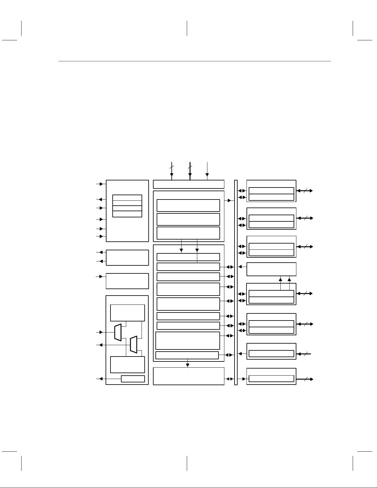
Functional Description for the MSP50C614
1.4 Functional Description for the MSP50C614
The MSP50C614 device consists of a micro-DSP core, embedded program
and data memory , and a self-contained clock generation system. General-purpose periphery is comprised of 64 bits of flexible I/O. The block diagram appearing in Figure 1–1 gives an overview of the MSP50C614/MSP50P614
functionality.
Figure 1–1. Functional Block Diagram for the MSP50C614/MSP50P614
SCANIN
SCANOUT
SCANCLK
SYNC
TEST
PGMPULSE
DACP
DACM
RESET
OSCIN
OSCOUT
PLL
Scan Interface
Break Point
Emulation
OTP Program
Serial Comm.
(C6xx only)
(P614 only)
DAC 0x30
32 Ohm PDM
Initialization
Logic
OSC Reference
Resistor
Trimmed
32 kHz nominal
or
or
Crystal
Referenced
32.768 kHz
PLL Filter
V
V
Power (P614 only)
(EP)ROM 32k x (16 + 1) bit
Test-Area
(reserved)
User ROM 0x0800 to
INT vectors 0x7FF0 to
Core
Instr. Decoder
PCU Prog. Counter Unit
CU Computational Unit
TIMER1 PRD1
TIMER2
Clock Control
Gen. Control
Interrupt Processor
DMAU
RAM 640 x 17 bit
(data)
DDVPP
SS
55
0x0000 to
0x3A
PRD2
0x3E
FLAG
0x39
Data Mem. Addr.
0x07FF
0x7FEF
0x7FFF
TIM1
0x3B
TIM2
0x3F
0x3D
0x38
MASK
0x38
0x000 to
0x027F
A port I/O
Data 0x00
Control 0x04
B port I/O
Data 0x08
Control 0x0C
C port I/O
Data 0x10
Control 0x14
Comparator
1 bit: PD5 vs PD
D port I/O
Data 0x18
Control 0x1C
E port I/O
Data 0x20
Control 0x24
F port INPUT
Data 0x28
G port OUTPUT
Data 0x2C
4
+ –
PA0–7
8
PB0–7
8
PC0–7
8
PD0–7
8
PE0–7
8
PF0–7
8
PG0–15
16
1-5Introduction to the MSP50C6xx
Page 20

Functional Description for the MSP50C614
The core processor is a general-purpose 16 bit micro-controller with DSP
capability. The basic core block includes a computational unit (CU), data
address unit, program address unit, two timers, eight level interrupt processor,
and several system and control registers. The core processor provides
break-point capability to the MSP50C6xx code development software
(EMUC6xx).
The processor is a Harvard type for efficient DSP algorithm execution. It requires separate program and data memory blocks to permit simultaneous access. The ROM has a protection scheme to prevent third-party pirating. It is
configured in 32K 17-bit words.
The total ROM space is divided into two areas: 1) The lower 2K words are reserved by T exas Instruments for a built-in self-test, 2) the upper 30K is for user
program/data.
The data memory is internal static RAM. The RAM is configured in 640 17-bit
words. Both memories are designed to consume minimum power at a given
system clock and algorithm acquisition frequency.
A flexible clock generation system is included that enables the software to
control the clock over a wide frequency range. The implementation uses a
phase-locked loop (PLL) circuit to generate the processor clock. The
Processor clock is programmable in 65.536-kHz steps between 64 kHz and
12.32 MHz. The PLL reference clock is also selectable; either a
resistor-trimmed oscillator or a crystal-referenced oscillator may be used.
Internal and peripheral clock sources are controlled separately to provide
different levels of power management (see Figure 1–2).
1-6
Page 21
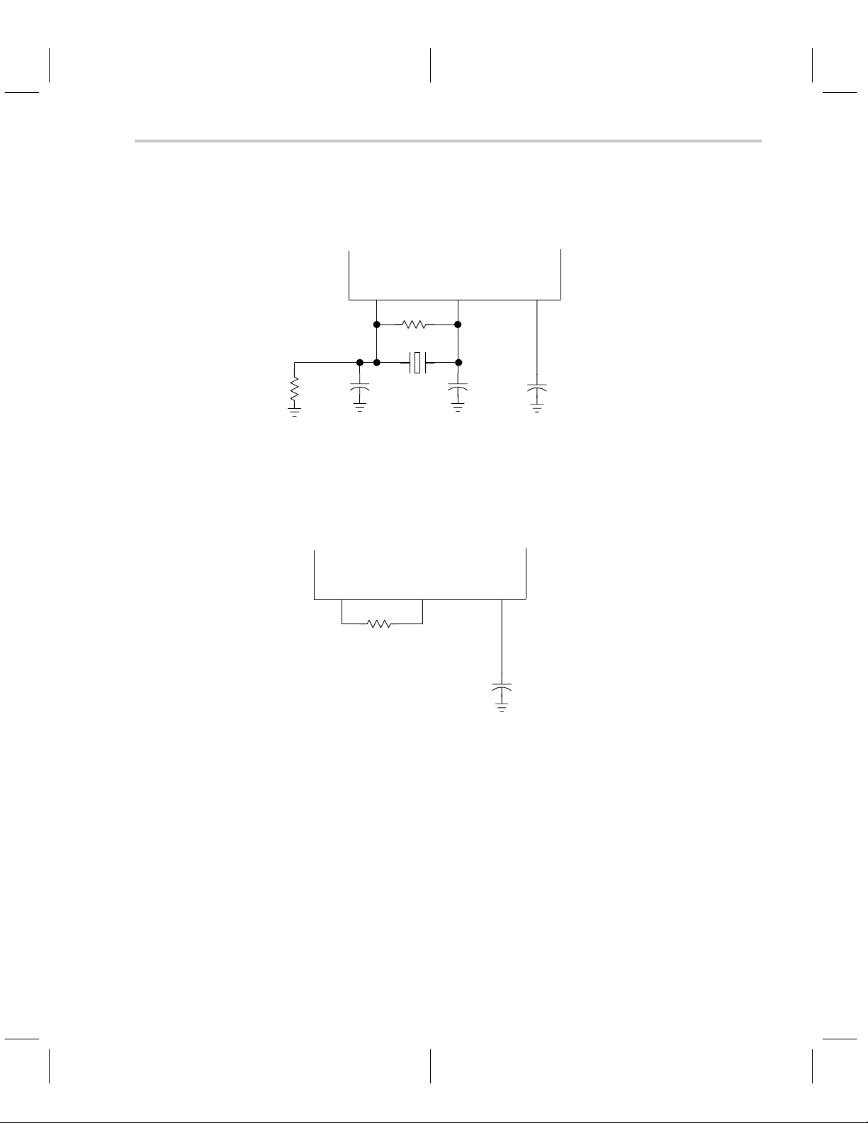
Figure 1–2. Oscillator and PLL Connection
a) Crystal Reference Oscillator Connections
OSCIN OSCOUT PLL
10 Mن
32.768 kHz†
Functional Description for the MSP50C614
MSP50P614
MSP50C6xx
10 Mن
†
Keep these components as close as possible to the OSCIN, OSC
22 pF†
b) Resistor Trim Oscillator Connections
MSP50C6xx
MSP50P614
OSCIN OSCOUT PLL
R
(RTO)
†
Keep these components as close as possible to the OSCIN, OSC
470 kΩ 1%†
=
The peripheral consists of five 8-bit wide general-purpose I/O ports, one 8-bit
wide dedicated input port, and one 16-bit wide dedicated output port. The
general-purpose I/O ports are bit-wise programmable as either
high-impedance inputs or as totem-pole outputs. They are controlled via
addressable I/O registers. The input-only port has a programmable pullup
option (100-kΩ minimum resistance) and a dedicated service interrupt. These
features make the input port especially useful as a key-scan interface.
22 pF†
, and PLL pins.
OUT
, and PLL pins.
OUT
C
(PLL)
C
= 3300 pF†
(PLL)
= 3300 pF†
A simple one-bit comparator is also included in the periphery . The comparator
is enabled by a control register, and its input pins are shared with two pins in
one of the general-purpose I/O ports.
1-7Introduction to the MSP50C6xx
Page 22
Functional Description for the MSP50C614
Rounding out the MSP50C6xx periphery is a built in pulse-density-modulated
(PDM) digital-to-analog converter (DAC) with direct speaker-drive capability.
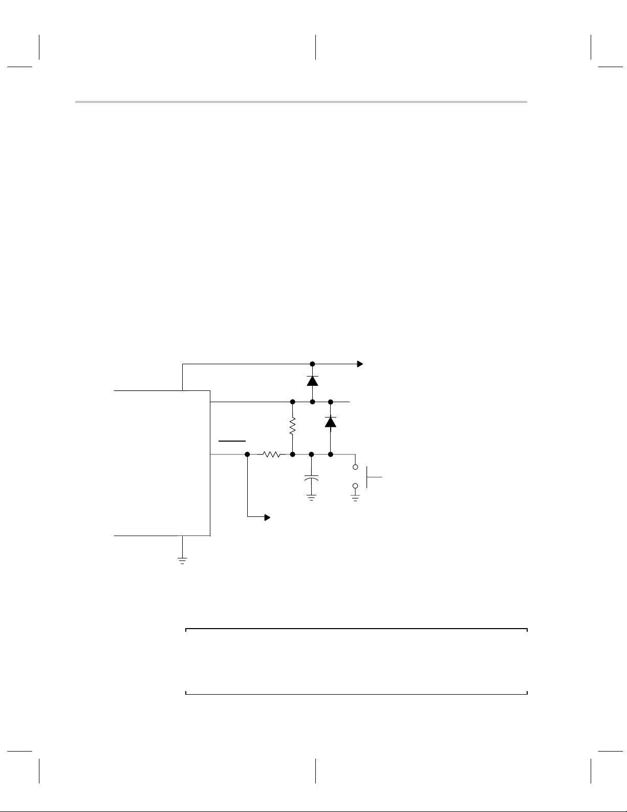
Typical connections to implement reset functionality are shown in Figure 1–3.
An external reset circuit is required to hold the reset pin low until the
MSP50C6xx power supply has stabilized in the specified voltage range. In
some cases, a simple reset circuit (as shown in Figure 1–3) can be used for
this purpose. However, this simple circuit may not be suitable for all applications. For example, if the power supply has an unpredictable rise time or has
intermittent voltage sags, the device may not initialize properly . The diode and
the switch shown in Figure 1–3 may be optional for some applications. The
diode provides a lower impedance path for the capacitor to discharge when
power is removed. This make the circuit more reliable when power is removed
and quickly reapplied.
Figure 1–3. RESET Circuit
(MSP50P614 only)
V
PP
V
DD
100 kΩ
†
Inside the
MSP50P614
MSP50C6xx
†
If it is necessary to use the software development tools to control the MSP50P614 in an application board, the 1 kΩ resistor is
needed to allow the development tool to over drive the RESET circuit on the application board.
‡
This Diode can be omitted (shorted) if the application does not require use of the scanport interface. See Section 7.1 regarding
scan port bond out.
RESET
V
SS
1 kΩ
1 µF
(20%)
To Pin 2 of optional (scan port) connector
IN914
To Pin 1 of Optional (Scanport)
Connector
‡
5 V
IN914
Reset
Switch
†
Note:
This simple circuit may not be suitable for all applications. For example, if the
power supply has an unpredictable rise time or has intermittent voltage sags,
the device may not initialize properly.
1-8
Page 23

MSP50C601, MSP50C604, and MSP50C605
1.5 MSP50C601, MSP50C604, and MSP50C605
Related products, the MSP50C601, MSP50C604, and MSP50C605 use the
MSP50C6xx core. The MSP50C601 has a 128K byte data ROM built into the
chip and 32 I/O port pins. The MSP50C605 has a 224K byte data ROM built
into the chip and 32 I/O port pins. The MSP50C604 has a 64K byte data ROM
built into the chip and 16 I/O port pins. The MSP50C601 can provide up to 24
minutes, the MSP50C605 can provide up to 37 minutes, and the MSP50C604
can provide up to 6.5 minutes of uninterrupted speech. The MSP50C604 is designed to support slave operation with an external host microcontroller. In this
mode the MSP50C604 can be programmed with a code that communicates
with the host via a command set. This command set can be designed to support LPC, CELP , MELP, and ADPCM coders by selecting the appropriate command. The MSP50C604 can also be used stand-alone in master mode. The
MSP50C601, MSP50C604, and MSP50C605 use the MSP50P614 as the development version device.
1-9Introduction to the MSP50C6xx
Page 24

1-10
Page 25

Chapter 2
MSP50C6xx Architecture
A detailed description of the MSP50C6xx architecture is included in this chapter. After reading this chapter , the reader will have in-depth knowledge of internal blocks, memory organization, interrupt system, timers, clock control mechanism, and various low power modes.
Topic Page
2.1 Architecture Overview 2–2. . . . . . . . . . . . . . . . . . . . . . . . . . . . . . . . . . . . . . . . .
2.2 Computation Unit 2–5. . . . . . . . . . . . . . . . . . . . . . . . . . . . . . . . . . . . . . . . . . . . .
2.3 Data Memory Address Unit 2–11. . . . . . . . . . . . . . . . . . . . . . . . . . . . . . . . . . .
2.4 Program Counter Unit 2–14. . . . . . . . . . . . . . . . . . . . . . . . . . . . . . . . . . . . . . .
2.5 Bit Logic Unit 2–14. . . . . . . . . . . . . . . . . . . . . . . . . . . . . . . . . . . . . . . . . . . . . . .
2.6 Memory Organization: RAM and ROM 2–15. . . . . . . . . . . . . . . . . . . . . . . .
2.7 Interrupt Logic 2–22. . . . . . . . . . . . . . . . . . . . . . . . . . . . . . . . . . . . . . . . . . . . . .
2.8 Clock Control 2–26. . . . . . . . . . . . . . . . . . . . . . . . . . . . . . . . . . . . . . . . . . . . . . .
2.9 Timer Registers 2–31. . . . . . . . . . . . . . . . . . . . . . . . . . . . . . . . . . . . . . . . . . . . .
2.10 Reduced Power Modes 2–33. . . . . . . . . . . . . . . . . . . . . . . . . . . . . . . . . . . . . .
2.11 Execution Timing 2–40. . . . . . . . . . . . . . . . . . . . . . . . . . . . . . . . . . . . . . . . . . .
2-1
Page 26

2.1 Architecture Overview
The core processor in the C6xx is a medium performance mixed signal processor with enhanced microcontroller features and a limited DSP instruction set.
In addition to its basic multiply/accumulate structure for DSP routines, the core
provides for a very efficient handling of string and bit manipulation. A unique
accumulator-register file provides additional scratch pad memory and minimizes memory thrashing for many operations. Five different addressing
modes and many short direct references provide enhanced execution and
code efficiency.
The basic elements of the C6xx core are shown in Figure 2–1. In addition to
the main computational units, the core’s auxiliary functions include two timers,
an eight-level interrupt processor, a clock generation circuit, a serial scan-port
interface, and a general control register.
2-2
Page 27
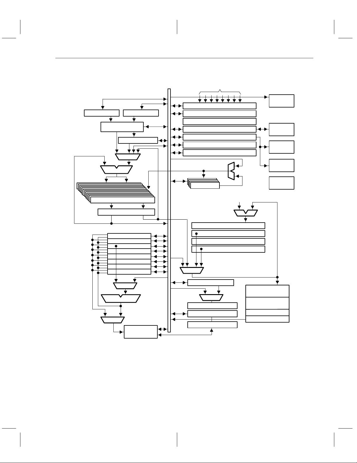
Figure 2–1. MSP50C6xx Core Processor Block Diagram
Interrupt Inputs
Interrupt Flag Register (IFR)†
Multiplier (MR)† Shift Value (SV)†
17 x 17 Multiplier
Product High (PH)†
MUX
16 bit ALU
32 Accumulators (AC0–AC31)†
Control Register (CTRL)†
Interrupt Processor
Serial Interface Register†
Oscillator Register†
Timer Period (PRD1 and PRD2)†
Timer Register (TIM1 and TIM2)†
AP0–AP3†
Accumulator Pointer
Peripheral
Interface
Serial
Interface
VCO
Frequency
Divider
Instruction
Decoder
+1
Column Exchange
Stack (R7)
Page (R6)
Index (R5)
Loop (R4)
R3
R2
R1
R0
MUX
Arithmetic Unit
MUX
Data Memory
640 x 17 bit
†
Indicates internal programmable registers.
Incrementor
Top Of Stack (TOS)†
Program Counter (PC)†
Protection Register (PR)†
Data Pointer (DP)†
MUX
String Register†
MUX
Repeat Counter†
Status Register (STAT)†
Flag Register†
Test Code
2k x 17 bit
Program Memory
30k x 17 bit
Macro Calls
Vectors
2-3MSP50C6xx Architecture
Page 28
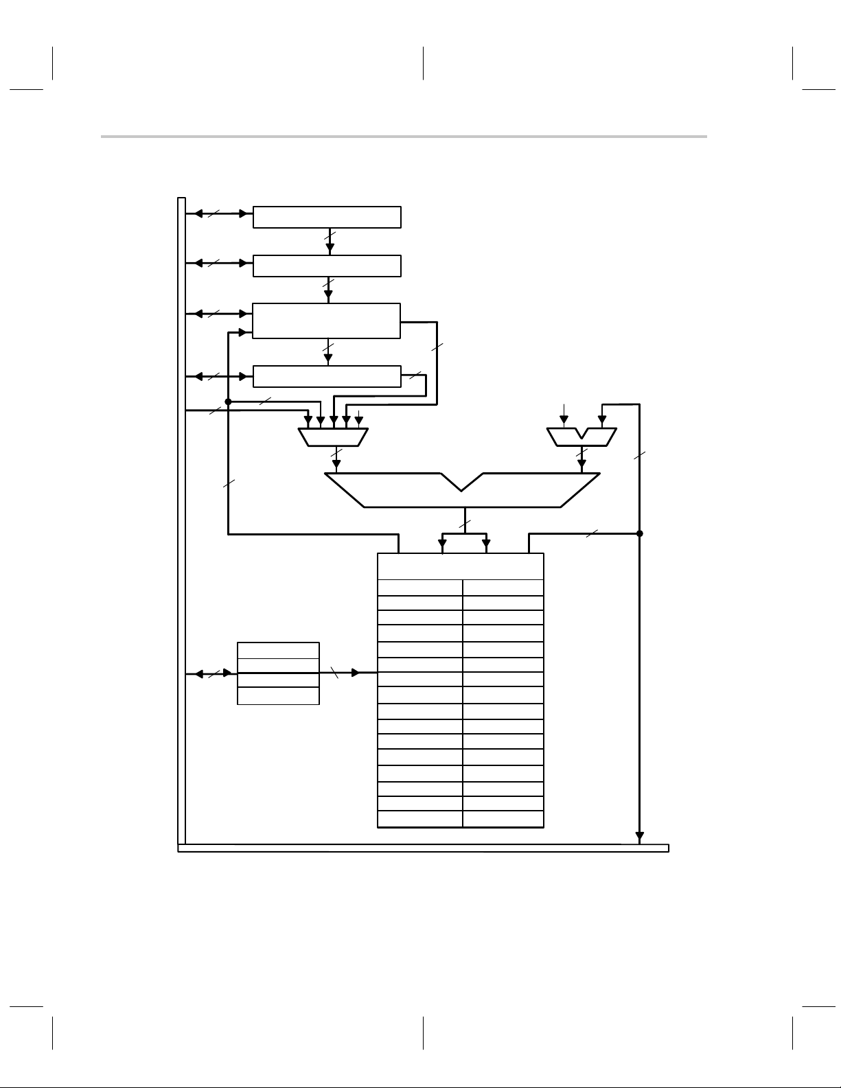
Figure 2–2. Computational Unit Block Diagram
16
16
16
16
16
16
5
Internal Databus – 16 bit
Shift Value (SV)
Multiplier Register (MR)
17 bit x 17 bit
Multiplexer
Product High (PH)
Accumulators
AP0
AP1
AP2
AP3
16
16
(Product Low, PL)
16 LSB
16 MSB
16
0
0
16
AB
ALU
16
Read/Write
AC0
AC1
AC2
AC3
AC4
5
AC5
AC6
AC7
AC8
AC9
AC10
AC11
AC12
AC13
AC14
AC15
AC16
AC17
AC18
AC19
AC20
AC21
AC22
AC23
AC24
AC25
AC26
AC27
AC28
AC29
AC30
AC31
16
16
2-4
Page 29

2.2 Computation Unit
The computational unit (CU) is comprised of a (17-bit by 17-bit) Booth’s
algorithm multiplier and a 16-bit arithmetic logic unit (ALU). The block diagram
of the CU is shown in Figure 2–2. The multiplier block is served by 4 system
registers: a 16-bit multiplier register (MR), a 16-bit write-only multiplicand
register, a 16-bit high word product register (PH), and a 4-bit shift value register
(SV). The output of the ALU is stored in one 16-bit accumulator from among
the 32 which compose the accumulator-register block. The accumulator
register block can supply either one operand to the ALU (addressed
accumulator register or its offset register) or two operands to the ALU (both the
addressed register and its offset).
2.2.1 Multiplier
The multiplier executes a 17-bit by 17-bit 2s complement multiply and
multiply-accumulate in a single instruction cycle. The sign bit within each
operand is bit 16, and its value extends from bit 0 (LSB) to bit 15 (MSB). The
sign bit for either operand (multiplier or multiplicand) can assume a positive
value (zero) or a value equal to the MSB (bit 15). In assuming zero, the extra
bit supports unsigned multiplication. In assuming the value of bit 15, the extra
bit supports signed multiplication. Table 2–1 shows the greater magnitude
achievable when using unsigned multiplication (65535 as opposed to 32767).
Computation Unit
Table 2–1. Signed and Unsigned Integer Representation
Unsigned Signed
Decimal Hex Decimal Hex
65535 0xFFFF −1 0xFFFF
32768 0x8000 −32768
32767 0x7FFF 32767
0
During multiplication, the lower word (LSB) of the resulting product, product
low, is multiplexed to the ALU. Product low is either loaded to or arithmetically
combined with an accumulator register. These steps are performed within the
same instruction cycle. Refer to Figure 2–3 for an overview of this operation.
At the end of the current execution cycle, the upper word (MSB) of the product
is latched into the product high register (PH).
0x0000 0 0x0000
0x8000
0x7FFF
2-5MSP50C6xx Architecture
Page 30

Computation Unit
The multiplicand source can be either data memory, an accumulator, or an
accumulator offset. The multiplier source can be either the 16-bit multiplier
register (MR) or the 4-bit shift value (SV) register. For all multiply operations,
the MR register stores the multiplier operand. For barrel shift instructions, the
multiplier operand is a 4-to-16-bit value that is decoded from the 4-bit shift
value register (SV).
As an example of a barrel shift operation, a coded value of 0x7 in the SV
register results in a multiplier operand of 0000000010000000 (1 at bit 7). This
causes a left-shift 7-times on the 16 bit multiplicand. The output result is 32-bit.
On the other hand, if the status bit FM (multiplier shift mode) is SET, then the
multiplier operand (0000000010000000) is left-shifted once to form a 17
significant-bit operand (00000000100000000). This mode is included to avoid
a divide-by-2 of the product, when interpreting the input operands as signed
binary fractions. The multiplier shift mode status bit is located in the status
register (STAT).
All three multiplier registers (PH, SV, and MR) can be loaded from data
memory and stored to data memory . In addition, data can be transferred from
an accumulator register to the PH, or vice versa. Both long and short constants
can be directly loaded to the MR from program memory.
The multiplicand is latched in a write-only register from the internal data bus.
The value is not accessible by memory or other system registers.
2-6
Page 31

Figure 2–3. Overview of the Multiplier Unit Operation
MULTIPLIER UNIT INPUTS
Computation Unit
Multiplicand 16-bit
- latched in a write-only register
from one of the following sources ...
Data Memory
Accumulator
Offset Accumulator
performs multiplication and barrel shifting
MSB 16-bit LSB 16-bit
(PH) Product High (PL) Product Low
- readable and writeable by Data Memory - a simulated register: PL is realized in ALU-A
- readable and writeable by ALU-A
†
Also write-able by Program Memory
X Multiplier
- writeable and readable by Data Memory
as one of the following ...
MULTIPLYING: 16-bit
SHIFTING:
MULTIPLIER UNIT
MULTIPLIER UNIT INPUTS
(MR)
(SV)
Multiplier Register†
or
Shift Value Register
2.2.2 Arithmetic Logic Unit
4-bit
The arithmetic logic unit is the focal point of the computational unit, where data
can be added, subtracted, and compared. Logical operations can also be
performed by the ALU. The basic hardware word-length of the ALU is 16 bits;
however, most ALU instructions can also operate on strings of 16-bit words
(i.e., a series or array of values). The ALU operates in conjunction with a
flexible, 16-bit accumulator register block. The accumulator register block is
composed of thirty-two, 16-bit registers which further enhances execution and
promotes compact code.
The ALU has two distinct input paths, denoted ALU-A and ALU-B (see
Figure-2–4). The ALU-A input selects between all zeros, the internal databus,
the product high register (PH), the product low (PL), or the offset output of the
accumulator register block. The ALU-B input selects between all zeros and the
output from the accumulator register block.
2-7MSP50C6xx Architecture
Page 32

Computation Unit
The all-zero values are necessary for data transfers and unitary operations.
All-zeros also serve as default values for the registers, which helps to minimize
residual power consumption. The databus path through ALU-A is used to input
memory values (RAM) and constant values (program memory) to the ALU.
The PH and PL inputs are useful for supporting multiply-accumulate
operations (refer to Section 2.2.1, Multiplier).
The operations supported by the ALU include arithmetic, logic, and
comparison. The arithmetic operations are addition, subtraction, and load
(add to zero). The logical operations are AND, OR, XOR, and NOT.
Comparison includes equal-to and not-equal-to. The compare operations may
be used with constant, memory, or string values without destroying any
accumulator values.
2.2.2.1 Accumulator Block
The output of the ALU is the accumulator block. The accumulator block is composed of thirty-two, 16-bit registers. These registers are organized into two terminals, denoted accumulator and OFFSET accumulator. The terminals provide references for all of the data which is to be held in the accumulator block.
The accumulator incorporates one-half of the 32 accumulator registers:
AC0..AC15. The OFFSET accumulator incorporates the other half:
AC16..AC31.
2-8
Page 33

Figure 2–4. Overview of the Arithmetic Logic Unit
ALU INPUTS
ALU-A 16-bit
Computation Unit
ALU-B 16-bit
- selects between ...
all 0’s
Offset Accumulator Register
Data Memory
Program Memory
(PH)
(PL)
16 × 16-bit registers ... 16 ×16-bit registers ...
AC0, AC1, AC2, AC3, AC4, AC5, AC6, AC7, AC8,
AC9, AC10, AC11, AC12, AC13, AC14, AC15
†
For multiply-accumulate operations.
Product High†
Product Low†
ARITHMETIC LOGIC UNIT
performs arithmetic, comparison, and logic
ALU OUTPUTS
THE ACCUMULATOR BLOCK
Accumulator Register OFFSET Accumulator Register
AC16, AC17, AC18, AC19, AC20, AC21, AC22,
AC23, AC24, AC25, AC26, AC27, AC28, AC29,
AC30, AC31
2.2.2.2 Accumulator Pointer Block
- selects between ...
all 0’s
Accumulator Register
There are four 5-bit registers which are used to store pointers to members of
the accumulator block. The accumulator pointers (AP0, AP1, AP2, AP3) are
used in two modes: 1) as a direct reference to one of 32, or 2) as an indirect
reference. The indirect reference includes a direct reference to one of 16 and
an offset (optional) which increments the reference by 16: AC(N+16). For
example, AC0 has its offset register located at AC16. AC1 has an offset
register located at AC17, and so on. The block is circular: address 31, when
incremented, results in address 0. The offsets of AC16 through AC31,
therefore, are AC0 through AC15, respectively (see Figure 2–5). Indirect
referencing by the AP pointers is supported by most of the C6xx’s
accumulator-referenced instructions.
2-9MSP50C6xx Architecture
Page 34

Computation Unit
When writing an accumulator-referenced instruction, therefore, the working
accumulator address is stored in one of AP0 to AP3. The C6xx instruction set
provides a two-bit field for all accumulator referenced instructions. The two-bit
field serves as a reference to the accumulator pointer which, in turn, stores the
address of the actual 16-bit accumulator. Some MOV instructions store the
contents of the APn directly to memory or load from memory to the APn
register. Other instructions can add or load 5-bit constants to the current APn
register contents. A full description of the C6xx instruction set is given in
Chapter 4, Assembly Language Instructions.
Figure 2–5. Overview of the Accumulators
Accumulator Block: 32, 16-bit registers AC(0) . . . AC(31)
Accumulator Block Pointers: 4, 5-bit registers AP(0) . . . AP(3)
The accumulator block pointers may assume values in one of two forms:
1) DIRECT REFERENCE:
2) INDIRECT REFERENCE: 0 . . . 15 points to: 0 . . . 15
– AP registers are served by a 5-bit processor for sequencing addresses or repetitive operations.
– Selection between the 4 AP’s is made in the 2-bit An field in all accumulator-referenced
instructions
2.2.2.3 String Operations
The AP registers are served by a 5-bit processor that provides efficient
sequencing of accumulator addresses. The design automates repetitive
operations like long data strings or repeated operations on a list of data.
When operating on a multiword data string, the address is copied from the AP
register to fetch the least significant word of the string. This copy is then
consecutively incremented to fetch the next n words of the string. At the
completion of the consecutive operations, the actual address stored in the AP
register is left unchanged; its value still points to the least significant location.
The AP register, therefore, is loaded and ready for the next repeatable
operation.
0 . . . 31
AC Register #
0 . . . 15 OFFSET points to: 16 . . . 31
15 . . . 31 OFFSET points to: 0 . . . 15
2-10
Page 35

Data Memory Address Unit
For some instructions, the 5-bit string processor can also preincrement or
predecrement the AP pointer-value by +1 or –1, before being used by the
accumulator register block. This utility can be effectively used to minimize
software overhead in manipulating the accumulator address. The
premodification of the address avoids the software pipelining effect that
post-modification would cause.
Some C6xx instructions reference only the accumulator register and cannot
use or modify the offset register that is fetched at the same time. Other instructions provide a selection field in the instruction word (A~ or ~A op-code bit).
This has the effect of exchanging the column addressing sense and thus the
source or order of the two registers. Also, some instructions can direct the ALU
output to be written either to the accumulator register or to the offset accumulator register. Refer to Chapter 4, Assembly Language Instructions, for more de-
tails.
The ALU’s accumulator block functions as a small workspace, which elimi-
nates the need for many intermediate transfers to and from memory . This alleviates the memory thrashing which frequently occurs with single accumulator designs.
2.3 Data Memory Address Unit
The data memory address unit (DMAU) provides addressing for data memory
(internal RAM). The block diagram of the DMAU is shown in Figure 2–6. The
unit consists of a dedicated arithmetic block and eight read/write registers (R0
through R7). Each read/write register is 16-bits in size. The arithmetic block
is used to add, subtract, and compare memory-address operands. The
register set includes four general-purpose registers (R0 to R3) and four
special-purpose registers. The special-purpose registers are: the LOOP
control register (R4), the INDEX register (R5), the P AGE register (R6), and the
STACK register (R7). The DMAU generates a RAM address as output. The
DMAU functions completely in parallel with the computational unit, which
helps the C6xx maintain a high computational throughput.
2-11MSP50C6xx Architecture
Page 36

Data Memory Address Unit
Figure 2–6. Data Memory Address Unit
Arithmetic Block
Internal
Databus
2.3.1 RAM Configuration
The data memory block (RAM) is physically organized into 17-bit parallel
words. Within each word, the extra bit (bit 16) is used as a flag bit or tag for
op-codes in the instruction set. Specifically , the flag bit directs complex branch
conditions associated with certain instructions. The flag bit is also used by the
computational unit for signed or unsigned arithmetic operations (see
Section 2.2.1, Multiplier).
R0
R1
R2
R3
R4
LOOP
R5
INDEX
R6
R7
PAGE
STACK
Register Addressing Mode
Internal Program Bus
RAM Address
The size of the C6xx RAM block is 640 17-bit locations. Each address provided
by the DMAU causes 17 bits of data to be addressed. These 17 bits are
operated on in different ways, depending on the instructions being executed.
For most instructions, the data is interpreted as 16-bit word format. This means
that bits 0 through 15 are used, and bit 16 is either ignored or designated as
a flag or status bit.
2-12
Page 37

Data Memory Address Unit
There are two-byte instructions, for example MOVB, which cause the processor to read or write data in a byte (8-bit) format. (The B appearing at the end
of MOVB designates it as an instruction that uses byte-addressable arguments.) The byte-addressable mode causes the hardware to read/write either
the upper or lower 8 bits of the 16-bit word based on the LSB of the address.
In this case, the address is a byte address, rather than a word address. Bits
0 through 7 within the word are used, so that a single byte is automatically rightjustified within the databus. Bits 8 through 15 may also be accessed as the upper byte at that same address.
A third data-addressing mode is the flag data mode, whereby , the instruction
operates on only the single flag bit (bit 16) at a given address. All flag mode
instructions execute in one instruction cycle. The flags can be referenced in
one of two addressing modes: 1) global address, whereby 64 global flags are
located at fixed locations in the first 64 RAM addresses, and 2) flag relative
address, whereby a reference is made relative to the current P AGE (R6). The
relative address supports 64 different flags whose PAGE-offset values are
stored in the PAGE register. The flag mode instructions cannot address
memory in the INDEX-relative modes. See Chapter 4, Assembly Language
Instructions, for more details.
2.3.2 Data Memory Addressing Modes
The DMAU provides a powerful set of addressing modes to enhance the performance and flexibility of the C6xx core processor. The addressing modes for
RAM fall into three categories:
-
Direct addressing
-
Indirect addressing with post-modification
-
Relative addressing
The relative addressing modes appear in three varieties:
-
Immediate Short, relative to the PAGE (R6) register.
The effective RAM address is: [*R6 + (a 7 bit direct offset)].
-
Relative to the INDEX (R5) register.
The effective RAM address is: [*R5 + (an indexed offset)].
-
Long Immediate, relative to the register base.
The effective RAM address is: [*Rx + (a 16 bit direct offset)].
Refer to Chapter 4, Assembly Language Instructions, for a full description of
how these modes are used in conjunction with various instructions.
2-13MSP50C6xx Architecture
Page 38

Program Counter Unit
2.4 Program Counter Unit
The program counter unit provides addressing for program memory (onboard
ROM). It includes a 16-bit arithmetic block for incrementing and loading
addresses. It also consists of the program counter (PC), the data pointer (DP),
a buffer register, a code protection write-only register, and a hardware loop
counter (for strings and repeated-instruction loops). The program counter unit
generates a ROM address as output.
The program counter value, PC, is automatically saved to the stack on various
CALL instructions and interrupt service branches. The stack consists of one
hardware-level register (TOS) which points to the top-of-stack. The TOS is
followed by a software stack. The software stack resides in RAM and is
addressed using the STACK register (R7) in indirect mode (see Section 2.3,
Data Memory Address Unit).
The hardware loop counter controls the execution of repeated instructions
using one of two modes: 1) consecutive iterations of a single instruction
following the repeat (RPT) instruction, or 2) a single instruction which operates
on a string of data values (string loops). For all types of repeated execution,
interrupt service branches are automatically disabled (temporarily).
2.5 Bit Logic Unit
The data pointer (DP) register is loaded at two instances: 1) from the
accumulator during lookup-table instructions, and 2) from the databus during
the fetch of long string constants. To simplify algorithms which require
sequential indices to lookup tables, the DP register may be stored in RAM.
The bit logic unit is a 1-bit unit which operates on flag bit data. It is controllable
by eleven different instructions, which generate the decision flags for
conditional program control. The results of operations performed by the bit
logic unit are sent either to the flag bit of RAM memory or to the TF1 and TF2
bits of the status register (STAT).
2-14
Page 39

2.6 Memory Organization: RAM and ROM
Data memory (RAM) and program memory (ROM) are each restricted to
internal blocks on the C6xx. The program memory is read-only and limited to
32K, 17-bit words. The lower 2048 of these words is reserved for an internal
test code and is not available to the user. The data memory is static RAM and
is limited to 640, 17-bit words. 16 bits of the 17-bit RAM are used for the data
value, while the extra bit is used as a status flag.
The C6xx does not have the capability to execute instructions directly from
external memory. However, additional program memory (external ROM) can
be accessed using the general-purpose I/O. The interface for external ROM
must be configured in the software.
2.6.1 Memory Map
The memory map for the C6xx is shown in Figure 2–7. Refer to Section 2.6.3,
Interrupt Vectors, for more detailed information regarding the interrupt vectors,
and to Section 2.6.2, Peripheral Communications (Ports), for more information
on the I/O communications ports.
Memory Organization: RAM and ROM
2-15MSP50C6xx Architecture
Page 40

Memory Organization: RAM and ROM
Figure 2–7. C6xx Memory Map (not drawn to scale)
Program Memory
0x0000
0x07FF
0x0800
0x7F00
0x7FF0
0x7FF7
0x7FF8
0x7FFE
0x7FFF
Internal Test Code
2048 x 17 bit
30704 x 17 bit
(C6xx : read-only)
(P614 : EPROM)
Macro Call Vectors
255 x 17 bit
(overlaps interrupt
vector locations)
Usable Interrupt
Unusable Interrupt
RESET vector
(reserved)
User ROM
Vectors
8 x 17 bit
Vectors
(reserved)
Data Memory
0x0000
0x027F
RAM
640 x 17 bit
Peripheral Ports
0x00
0x04
0x08
0x0C
0x10
0x14
0x18
0x1C PD
0x20
0x24
0x28
0x2C
0x2F
0x30
0x34
0x38
0x39
0x3A
PA
PA
PB
PB
PC
PC
PD
PE
PE
PF
PG
RTRIM
DAC data
DAC ctrl
IntGenCtrl
IFR
PRD1
0–7
0–7
0–7
0–7
0–7
0–7
0–7
0–7
0–7
0–7
0–7
0–15
data
ctrl
data
ctrl
data
ctrl
data
ctrl
data
ctrl
data
data
Shaded boxes highlight dedicated ROM and control registers.
2.6.2 Peripheral Communications (Ports)
Peripheral functions in the C6xx are controlled using one or more of the I/O
address-mapped communications ports. Table 2–2 describes the ports.
The width of each mapped location, shown in width of location, is independent
of the address spacing. In other words, some registers are smaller in width
than the spacing between neighboring addresses. The few unused bits appear
to the right of the LSB values within the DAC Data register, address 0x30 (refer
to Section 3.2.2, DAC Control and Data Registers).
2-16
0x3B
0x3D
0x3E
0x3F
TIM1
ClkSpdCtrl
PRD2
TIM2
Page 41

Memory Organization: RAM and ROM
When writing to any of the locations in the I/O address map, therefore, the
bit-masking need only extend as far as width of location. Within a 16-bit
accumulator, the desired bits (width of location) should be right-justified. The
write operation is accomplished using the OUT instruction, with the address
of the I/O port as an argument.
A read from these locations is accomplished using the IN instruction, with the
address of the I/O port as an argument. When reading from the I/O port to a
16-bit accumulator, the IN instruction automatically clears any extra bits in
excess of width of location. The desired bits in the result will be right-justified
within the accumulator.
Allowable access indicates whether the port is bidirectional, read-only, or
write-only. The last column of the table points to the section in this manual
where the functions of each bit have been defined in more detail.
Table 2–2. Summary of MSP50C614’s Peripheral Communications Ports
I/O Map
Address
0x00 8 bits Read & Write I/O port A data PA
0x04 8 bits Read & Write I/O port A control PA
0x08 8 bits Read & Write I/O port B data PB
0x0C 8 bits Read & Write I/O port B control PB
0x10 8 bits Read & Write I/O port C data PC
0x14 8 bits Read & Write I/O port C control PC
0x18 8 bits Read & Write I/O port D data PD
0x1C 8 bits Read & Write I/O port D control PD
0x20 8 bits Read & Write I/O port E data PE
0x24 8 bits Read & Write I/O port E control PE
0x28 8 bits Read Only Input port F data PF
0x2C 16 bits Read & Write Output port G data PG
0x2F 17 bits Read Only
0x30 16 bits Write Only DAC data DAC Data 0x0000 3.2.2
Width of
Location
Allowable
Access
Control Register
Name
RTO oscillator trim
adjustment
Abbreviation
Data unknown†
0..7
Ctrl 0x00 ‡
0..7
Data unknown
0..7
Ctrl 0x00
0..7
Data unknown
0..7
Ctrl 0x00
0..7
Data unknown
0..7
Ctrl 0x00
0..7
Data unknown
0..7
Ctrl 0x00
0..7
Data unknown 3.1.2
0..7
Data 0x0000 3.1.3
0..15
RTRIM 0x0000 2.8.4
State after
RESET LOW
Section for
Reference
3.1.1
0x34 4 bits Read & Write DAC control DAC Ctrl 0x0 3.2.2
0x38 16 bits Read & Write Interrupt/general Ctrl IntGenCtrl 0x0000 3.4
†
Input states are provided by the external hardware.
‡
A control register value of 0x00 yields a port configuration of all inputs.
2-17MSP50C6xx Architecture
Page 42

Memory Organization: RAM and ROM
2.8
2.8
Table 2–2. Summary of C614’s Peripheral Communications Ports (Continued)
I/O Map
Address
0x39 8 bits Read & Write Interrupt flag IFR
0x3A 16 bits Read & Write TIMER1 period PRD1 0x0000
0x3B 16 bits Read & Write TIMER1 count-down TIM1 0x0000
0x3D 16 bits Write Only Clock speed control ClkSpdCtrl 0x0000 2.9.3
0x3E 16 bits Read & Write TIMER2 period PRD2 0x0000
0x3F 16 bits Read & Write TIMER2 count-down TIM2 0x0000
Width of
Location
Allowable
Access
Control Register Name Abbreviation
State after
RESET LOW
Same state as
before RESET
2.6.3 Interrupt Vectors
When its event has triggered and its service has been enabled, an interrupt
causes the program counter to branch to a specific location. The destination
location is stored (programmed) in the interrupt vector, which resides in an upper address of ROM. The following table lists the ROM address associated
with each interrupt vector:
Interrupt Name
INT0 0x7FF0 DAC Timer Highest
INT1 0x7FF1 TIMER1 2nd
INT2 0x7FF2 TIMER2 3rd
INT3 0x7FF3 port D
INT4 0x7FF4 port D
INT5 0x7FF5 all port F 6th
INT6 0x7FF6 port D
INT7 0x7FF7 port D
RESET
ROM address of
Vector
Event Source Interrupt Priority
2
3
4
5
0x7FFE storage for ROM Protection Word
0x7FFF storage for initialization vector
Section for
Reference
2.7
4th
5th
7th
Lowest
Note: ROM Locations that Hold Interrupt Vectors
ROM locations that hold interrupt vectors are reserved specifically for this
purpose. Additional ROM locations 0x7FF8 - 0x7FFD are reserved for future
expansion. Like the interrupt vectors, they should not be used for general
program storage.
2-18
Page 43

The branch to the program location that is specified in the interrupt vector is,
of course, contingent on the occurrence of the trigger event. Refer to Section
3.1.5, Internal and External Interrupts, for more information regarding the
specific conditions for each interrupt-trigger event. The branch operation,
however, is also contingent on whether the interrupt service has been enabled.
This is done individually for each interrupt, using the interrupt mask bits within
the interrupt/general control register. Refer to Section 2.7, Interrupt Logic, for
more details.
The ROM location 0x7FFF holds the program destination associated with the
hardware RESET event (branch happens after RESET LOW-to-HIGH). The
location 0x7FFE holds the read/write block-protection word. Refer to Section 2.6.4, ROM Code Security, for an explanation of the ROM security
scheme.
2.6.4 ROM Code Security
The C6xx provides a mechanism for protecting its internal ROM code from
third-party pirating. The protection scheme is composed of two levels, both of
which prevent the ROM contents from being read. Protection may be applied
to the entire program memory, or it can be applied to a block of memory
beginning at address 0x0000 and ending at an arbitrary address. The two
levels of ROM protection are designated as follows:
Memory Organization: RAM and ROM
-
Direct read and write protection, via the ROM scan circuit.
-
Indirect read protection, which prohibits the execution of memory-lookup
instructions.
For the purposes of direct security , the ROM is divided into two blocks. The first
block begins at location 0x0000, and ends, inclusively, at location
(m × 512 – 1), where m is some integer . Each address specifies a 17-bit word
location. The second block begins at location (m × 512), and ends, inclusively ,
at 0x7FFF (the end of the ROM). The first block is protected from reads and
writes by programming a block protection bit, and the second block is
protected from reads and writes by programming a global protection bit.
The two-block system is designed in such a way that a secondary developer
is prevented from changing the partition address between blocks. Once the
block protection has been engaged, then the only security option available to
the secondary developer is engaging the global protection.
2-19MSP50C6xx Architecture
Page 44

Memory Organization: RAM and ROM
Note: Instructions with References
Care must be taken when employing instructions that have either long string
constant references or look-up table references. These instructions will
execute properly only if the address of the instruction and the address of the
data reference are within the same block.
The protection modes are implemented on the C6xx as follows. Within the
ROM is a dedicated storage for the block protection word (address 0x7FFE).
The block protection word is divided into two 6-bit fields and two single-bit
fields. The remainder of the 17-bit word is broken into three single-bit fields
which are reserved for future use.
Block Protection Word
address 0x7FFE (17-bit wide location)
WRITE only 16 15 14 13 12 11 10 09 08 07 06 05 04 03 02 01 00
R R TM TM TM TM TM TM GP BP R FM FM FM FM FM FM
05 04 03 02 01 00 05 04 03 02 01 00
TM : True Protection Marker (NTM) GP : Global Protection (0 value protects)
FM : False Protection Marker (NFM) BP : Block Protection (0 value protects)
R : Reserved for future use (must be 1) 1 : Default value of cells on erasure
The two 6-bit fields are designated as the true protection marker, (TM5 through
TM0) and the false protection marker, (FM5 through FM0). When setting up
a partition for partial ROM protection, the address of the partition must be specified as:
2-20
Page 45

Memory Organization: RAM and ROM
[(NTM + 1) * 512 – 1] = highest ROM address within the block to be
protected
+ 1) * 512 = lowest ROM address which is left unprotected
(N
TM
N
TM
= the value programmed at TM5…TM0 (true
protection marker)
N
N
FM
FM
≡ the binary complement of N
TM
= the value programmed at FM5…FM0 (false
protection marker)
The purpose of the true and false protection markers is to provide parity. An
erased P614 EPROM cell defaults to the value 1. Once programmed from 1
to 0, it cannot be programmed back to 1, unless the cell (and all other cells
along with it) are subject to erasure. A multi-pass programming, therefore, can
only lower the value stored at an EPROM address and never raise it. Once a
valid block-partition address has been properly specified in both TM and FM,
it is impossible to change TM to another address and still maintain parity with
FM.
Note: Block Protection Mode
When applying the block protection mode, bits FM5 through FM0 must be
programmed as the logical inverse of bits TM5 through TM0, respectively.
Across the span of the 32k word ROM space, there are 64 possible values for
(including zero). Hence, the 6-bit-wide locations for TM and FM.
N
TM
The two single-bit fields found within the block protection word are the block
protection bit (BP) and the global protection bit (GP). If BP and GP are both
SET (erased), then no protection is applied to the ROM.
If BP is CLEAR and GP is SET, then the block protection mode is engaged.
This means that read and write access is prevented at locations 0x0000
through [(N
+ 1) × 512] through 0x7FFF.
[(N
TM
+ 1) × 512 – 1]. Read and write access is permitted at locations
TM
If GP is CLEAR, then the global protection mode is engaged. This prevents
read and write access to all addresses of the ROM, regardless of the value of
BP.
Note: Block Protection Word
The remaining bits in the block protection word are reserved for future use,
but must remain set in order to ensure future compatibility. These bits are
numbers 6, 15, and 16.
2-21MSP50C6xx Architecture
Page 46

Interrupt Logic
When the device is powered up, the hardware initialization circuit reads the
value stored in the block protection word. The value is then loaded to an internal register and the security state of the ROM is identified. Until this occurs,
execution of any instructions is suspended.
The same initialization sequence is executed before entry into the special
test-modes available on the P614 and C6xx (EPROM mode, emulation mode,
and trace mode). This insures that the protection scheme is always in force
when running the processor in one of these modes. A dedicated circuit
ensures that a switch between emulation mode and trace mode cannot occur
without going through the initialization (security check). This forces all look-up
tables and long constant references to originate from an external program
source, when in emulation mode. It is possible to switch from trace mode to
emulation mode by lowering V
jeopardize code security.
2.6.5 Macro Call Vectors
Macro call vectors are similar to CALL instructions except they take an 8-bit
address. The upper 8 bits is always 7Fh. See Section 4.14.84, VCALL, for
more information on the VCALL instruction.
, but this transition, by design, does not
PP
2.7 Interrupt Logic
2-22
An eight-level interrupt system is included as part of the C6xx’s core processor .
The initialization and control of these interrupts is governed by the following
components: the global interrupt enable, the interrupt flag register, the
interrupt mask register, and the interrupt service branch. Each of these is
described below.
Interrupts must be globally enabled using the INTE instruction, and they are
globally disabled using the INTD instruction. INTE sets the global interrupt
enable bit, and INTD clears the global interrupt enable bit. The state of this bit
specifically determines whether any interrupt service branches will be taken.
The global interrupt enable appears as bit 4 within the status register (ST AT).
Note:
T o ensure proper executions of the INTD instruction, it is recommended that
the INTD instruction be prescaled with a RPT 2–2 instruction.
Each interrupt level waits for the conditions of its trigger event (refer to
Figure 2–8). At the time that a trigger event occurs, the respective bit is
Page 47

automatically SET in the interrupt flag register (IFR). The IFR is an 8-bit wide
port-addressed register; wherein, each interrupt level is represented. A set bit
in the IFR indicates that the interrupt is pending and waiting to be serviced. A
clear bit indicates that the interrupt is not currently pending. The address of the
IFR is 0x39. After a RESET low, the IFR is left in the same state it was before
the RESET low, assuming there is no interruption in power. For a full
description of the interrupt-trigger events, refer to Section 3.1.5, Internal and
External Interrupts.
(8-bit wide location)
07 06 05 04 03 02 01 00 ← INT number
IFR
Interrupt Flag register
address 0x39
D5 : port D5 falling-edge
D4 : port D4 rising-edge
D3 : port D3 falling-edge T1 : TIMER1 underflow
†
†
D5
D4 PF D3 D2 T2 T1 DA
low high
priority priority
PF : any port F falling-edge
T2 : TIMER2 underflow
Interrupt Logic
D2 : port D2 rising-edge DA : DAC timer underflow
1 : A bit value 1 indicates pending interrupt waiting to be serviced.
RESET: The IFR is left in the same state it was before RESET low, assuming no interruption in power.
†
INT6 and INT7 may be associated instead with the Comparator function, if the Comparator Enable bit has been set. Refer to
Section 3.3, Comparator, for details.
Individual interrupts are enabled or disabled for service by setting or clearing
the respective bit in the interrupt mask register (IMR, 8 bits). If an interrupt level
has its bit cleared in the IMR, then the interrupt service associated with that
interrupt is disabled. Setting the bit in the IMR allows service to occur (pending
the trigger-event which is registered in the IFR).
The IMR is accessible as part of another (larger) register, namely, the
interrupt/general control register (peripheral port 0x38). After a RESET LOW,
the default value of each bit in the IMR is zero: no interrupt service enabled.
A full description of the bit locations in the interrupt/general control register can
be found in Section 3.4, Interrupt/General Control Register.
The IMR functions independently of the IFR, in the sense that interrupt-trigger
events can be registered in the IFR, even if the respective IMR bit is clear. Both
the IFR and IMR are readable and writeable as port addressed registers. To
read the register, use the IN instruction in conjunction with the port address
(0x38 or 0x39). Use the OUT instruction to write. (Refer to Section 2.6.2,
Peripheral Communications (Ports), for more information.)
2-23MSP50C6xx Architecture
Page 48

Interrupt Logic
Note: Setting a Bit in the IFR Using the OUT Instruction
Setting a bit within the IFR using the OUT instruction is a valid way of obtaining a software interrupt. An IFR bit may also be cleared, using OUT, at any
time.
Assuming the global interrupt enable is set and the specific bit within the IMR
is set, then, at the time of the interrupt-trigger event, an interrupt service
branch is initiated. (The trigger event is marked by a 0-to-1 transition in the IFR
bit). At that time, the core processor searches all interrupt levels which have
both: 1) pending interrupt flag, and 2) interrupt service enabled. The highest
priority interrupt among these is selected. The program then branches to the
location which is stored in the associated Interrupt Vector (Section 2.6.3, Inter-
rupt Vectors). This location constitutes the start of the interrupt service routine.
Instructions in the interrupt service routine are executed until the IRET (return)
instruction is encountered. Afterwards, any other pending interrupts will be
similarly serviced, in the order of their priority . Eventually , the program returns
to whatever point it was before the first interrupt service branch.
When an interrupt service branch is taken, the global interrupt enable is
automatically cleared by the core processor. This disables all further interrupt
service branches while still in the pending service routine. As a result, the
programmer must re-enable the interrupts globally using the INTE instruction.
If performed as the second-to-last instruction in the service routine, then no
nesting of multiple interrupts will occur. If, on the other hand, a nesting of
certain interrupts is desired, then the INTE instruction may be included as the
first instruction (or anywhere else) within the service routine.
When an interrupt service branch is taken, the processor core also clears
another status, namely , the respective bit in the IFR. This action automatically
communicates to the IFR that the current pending interrupt is now being
serviced. Once cleared, the IFR bit is ready to receive another SET whenever
the next trigger event occurs for that interrupt.
Note: Interrupt Service Branch
If the interrupt service branch is not enabled by the respective bit in the mask
register, then neither the global interrupt enable nor the respective flag bit is
cleared. No program vectoring occurs.
2-24
Page 49

Figure 2–8 provides an overview of the interrupt control sequence. INT0 is the
highest priority interrupt, and INT7 is the lowest priority interrupt.
Figure 2–8. Interrupt Initialization Sequence
Interrupt Logic
INTD
instruction
INTE
instruction
CLEAR
SET
Global Interrupt Enable
CLEAR
CLEAR BIT
Associated With the Interrupt-Trigger Event
INT7 INT6 INT5 INT4 INT3 INT2 INT1 INT0
Interrupt / General Control Register (0x38)†
INT7 INT6 INT5 INT4 INT3 INT2 INT1 INT0
Interrupt-Trigger Event
• Internal Timer Underflow
• External Input Falling-Edge
• External Input Rising-Edge
• Software Write Instruction
INT Flag bits (IFR)
Interrupt Flag Register (0x39)
INT Mask bits (IMR)
Specific Enable for Interrupt Service
†
SET BIT
Interrupt
Service
Routine
(1 of 8)
INTE
IRET
†
The port-addressed write instruction (OUT) can be used to SET or CLEAR bits in the IFR and IMR.
Interrupt Service Branch
Highest Priority INT is Selected From
Among Those Flagged and Enabled.
Program Branches to Location
Stored in Interrupt Vector.
Interrupt Vector Storage
0x7FF0 0x7FF2 0x7FF4 0x7FF6
0x7FF1 0x7FF3 0x7FF5 0x7FF7
2-25MSP50C6xx Architecture
Page 50

Clock Control
In addition to being individually enabled, all interrupts must be GLOBALLY
enabled before any one can be serviced. Whenever interrupts are globally
disabled, the interrupt flag register may still receive updates on pending trigger
events. Those trigger events, however, are not serviced until the next INTE
instruction is encountered.
After an interrupt service branch, it is the responsibility of the programmer to
re-SET the global interrupt enable, using the INTE instruction.
2.8 Clock Control
2.8.1 Oscillator Options
The C6xx has two oscillator options available. Either option may be enabled
using the appropriate control bits in the clock speed control register
(ClkSpdCtrl). The ClkSpdCtrl is described in Section 2.9.3, Clock Speed Con-
trol Register.
The first oscillator option, called the resistor-trimmed oscillator (RTO), is useful
in low-cost applications where accuracy is less critical. This option utilizes a
single external resistor to reference and stabilize the frequency of an internal
oscillator. The oscillator is designed to run nominally at 32 kHz. It has a low V
coefficient and a low temperature coefficient (refer to the data sheet). The
reference resistor is mounted externally across pins OSCIN and OSC
RTO oscillator is insensitive to variations in the lead capacitance at these pins.
The required value of the reference resistor is 470 kΩ (1%).
OUT
DD
. The
The second oscillator option, CRO for crystal referenced, is a real time clock
utilizing a 32.768 kHz crystal. The crystal is mounted externally across pins
OSC
2.8.2 PLL Performance
A software controlled PLL multiplies the reference frequency (generated from
either RTO or CRO) by integer multiples. This higher frequency drives the
master clock which, in turn, drives the CPU clock. The master clock (MC)
drives the circuitry in the periphery sections of the C6xx. The CPU Clock drives
the core processor; its rate determines the overall processor speed. The multiplier in the PLL circuit, therefore, allows the master clock and the CPU clock
to be adjusted between their minimum and maximum values.
For either oscillator option, the reference frequency (32.768 kHz) is multiplied
by four before it is accessed by the PLL circuit. The base frequency for the PLL,
2-26
and OSC
IN
OUT
.
Page 51

therefore, is 131.07 kHz, and the multiplier operates in increments of this base
frequency. The minimum multiplication of the base frequency is 1, and the
maximum multiplication is 256. The resulting master clock frequency, therefore, can be varied from a minimum of 131.07 kHz to a maximum of
33.554 MHz, in 131.07 kHz steps.
From the master clock to the CPU clock, there is a divide-by-two in frequency .
The CPU clock, therefore, can be set to run between 65.536 kHz and the maximum achievable (refer to the data sheet), in 65.536 kHz steps.
The maximum required CPU clock frequency for the C6xx is 8 MHz over the
entire V
CPU clock frequencies may be achieved, but these are not qualified over the
complete range of supply voltages in the guaranteed specification.
Figure 2–9. PLL Performance
Clock Control
range. This rate applies to the speed of the core processor. Higher
DD
Oscillator Reference
32 kHz
Resistor
Trimmed
RTO CRO
Selection Made in ClkSpdCtrl
Phase-Locked-Loop circuit
Multiplier Adjusted in ClkSpdCtrl
or
x4
PLL
x 1 ... x 256
crystal
referenced
Timer Source Option
Selected in IntGenCtrl
1
0
1
0
÷2
÷2
CPU Clock
(F
MAX
MC
= 8 MHz)
Master Clock : Runs Periphery
131.07 kHz ... 33.554 MHz
Core-Processor Speed
65.536 kHz ... F
TIMER2
MAX
TIMER2
2-27MSP50C6xx Architecture
Page 52

Clock Control
2.8.3 Clock Speed Control Register
The ClkSpdCtrl is a 16-bit memory mapped register located at address 0x3D.
The reference oscillator (RTO or CRO) is selected by setting one of the two
control bits located at bits 8 and 9. Setting bit 8 configures the C6xx for the RTO
reference option and simultaneously starts that oscillator. Setting bit 9
configures the C6xx for the CRO reference option and simultaneously pulses
the crystal, which starts that oscillator.
Note: ClkSpdCtrl Bits 8 and 9
When bit 8 is set in the ClkSpdCtrl register, the crystal oscillator bit (bit 9) becomes the least significant bit of the 6-bit resistor trim value. Thus, bits 15–11
and 9 make up the 6-bit resistor trim value. For example, if the ClkSpdCtrl
register is 00010X11XXXXXXXX (X means don’t care, bold numbers are re-
sistor trim bits), then the resistor trim value is equal to five.
The default value of the ClkSpdCtrl is 0x0000, which means that neither option
is enabled by default. Immediately after a RESET LOW-to-HIGH, and
regardless of whether a resistor or a crystal is installed across OSC
OSC
absence of a reference, however, the PLL still oscillates; it bottoms-out at a
minimum frequency . The master clock, in turn, runs at a very slow frequency
(less than 100 kHz) in the absence of a reference oscillator. Under this
condition, program execution is supported at a slow rate until one of the two
references (RTO or CRO) is enabled in software. (Refer to the data sheets for
the MSP50Cxx devices).
, the C6xx does not have a reference oscillator running. In the
OUT
IN
/
Once a reference oscillator has been enabled, the speed of the master clock
(MC) can be set and adjusted, as desired. Bits 7 through 0 in the ClkSpdCtrl
constitute the PLL multiplier (PLLM). The value written to the PLLM controls
the effective scaling of the MC, relative to the 131.07 kHz base frequency. A
0 value in PLLM yields the minimum multiplication of 1, and a 255 value in
PLLM yields the maximum multiplication of 256. The resulting MC frequency ,
therefore, is controlled as follows:
MC Master clock frequency kHz = (PLLM register value + 1) × 131.07 kHz
CPU Clock frequency kHz = (PLLM register value + 1) × 65.536 kHz
2-28
Page 53

Clock Control
The configuration of bits in the clock speed control register appears below:
ClkSpdCtrl register
address 0x3D (16-bit wide location)
WRITE only 15 14 13 12 11 10 09 08 07 06 05 04 03 02 01 00
T5 T4 T3 T2 T1 I C or T0 R MMMMMMMM
T : RTO oscillator-Trim adjust R : enable Resistor-trimmed oscillator
I : Idle State clock Control M : PLLM multiplier bits for MC
C : enable Crystal oscillator
(or T0 if R is set
Bit 10 in the ClkSpdCtrl is idle state clock control. The level of deep-sleep
generated by the IDLE instruction is partially controlled by this bit. When this
bit is cleared (default setting), the CPU clock is stopped during the sleep, but
the MC remains running. When the idle state clock control bit is set, both the
CPU clock and the MC are stopped during sleep. Refer to section 2.1 1 for more
information regarding the C6xx’s reduced-power modes.
Note: Reference Oscillator Stopped by Programmed Disable
If the reference oscillator is stopped by a programmed disable, then, on reenable, the oscillator requires some time to restart and resume its correct frequency. This time imposes a delay on the core processor resuming fullspeed operation. The time-delay required for the CRO to start is GREA TER
than the time-delay required for the RTO to start.
2.8.4 RTO Oscillator Trim Adjustment
Bits 15 through 11 and bit 9 (6 bits total) in the ClkSpdCtrl effect a software
control for the RTO oscillator frequency. The purpose of this control is to trim
the RTO to its rated (32 kHz) specification. The correct trim value varies from
device to device. The user must program bits 15 through 1 1 and 9, in order to
achieve the 32-kHz specification within the rated tolerances. Texas
Instruments provides the trim value to the programmer of the P614 part with
a sticker on the body of the chip. For the C6xx parts, the correct trim value is
located at I/O location 0x2Fh.
0x0000 : default state after RESET LOW
2-29MSP50C6xx Architecture
Page 54

Clock Control
RTRIM Register (Read Only) (Applies to MSP50C6xx Device Only)
I/O Address 0x2Fh (17-bit wide location)
16 15 14 13 12 11 10 09 08 07 06 05 04 03 02 01 00
RRRRRRRRRRRT5T4T3T2T1T0
T: RTO oscillator-trim storage (device specific)
R: reserved for Texas Instruments use
ClkSpdCtrl Value Copied (Shaded)
15 14 13 12 11 10 9 8 7 6 5 4 3 2 1 0
T5 T4 T3 T2 T1 I T0 1 M7 M6 M5 M4 M3 M2 M1 M0
When selecting and enabling the RTO oscillator ,therefore, the bits at positions
05 through 01 should be read from I/O location 0x2F (MSP50C6xx device
only), then copied to the ClkSpdCtrl trim adjust (bits 15 through 11 of control
register 0x3D), and bit 0 of 0x2F I/O port should be copied to bit 9 of ClkSpdCtrl
register. The bit ordering is the same; bit 04 of I/O 0x2F copies to bit 15 of
register 0x3D. Likewise, bit 00 of I/O 0x2F copies to bit 9 of register 0x3D.
However, the general specification of the adjustment can be useful in certain
circumstances. For example, the adjustment can be used to obtain a programmatic increase or decrease in the speed of the RTO reference. The default value for the adjustment, after RESET low, is all zeros. The zero value generates
the slowest programmable rate for the RTO reference. The maximum value,
0x3F , generates the fastest programmable rate for the RTO reference. The full
range from 0x00 to 0x3F , ef fects an approximate +62% change (based on the
RTO resistor value specification).
On the P614 part, the above method does not cause in the correct trim value
to be loaded in ClkSpdCtrl. MSP50P614 is an EPROM device. Any
preprogrammed value is erased when the chip goes through a UV erase
procedure. The RTO trim value must, therefore, be computed separately for
each chip. RTO trim values differ from one chip to another, is identical for the
same chip.
Note: Register Trim Value
A resistor trim value is only needed when the resistor trimmed oscillator
(RTO) is used. The MSP50P614 device must determine the trim value separately and use this value in the ClkSpdCtrl register bits 15–1 1 and 9, but C6xx
device needs to copy bit 0 of I/O location 0x2F to bit 9 of the ClkSpdCtrl register and bits 5 through 1 to bits 15 through 11 of ClkSpdCtrl register.
2-30
Page 55

This software-controlled trim for the RTO is not a replacement for the external
reference-resistor mounted at pins OSCIN and OSC
adjustment has no effect on the rate of the CRO reference oscillator.
2.9 Timer Registers
The C6xx contains two identical timers, TIMER1 and TIMER2. Each includes
a period register and a count-down register. The period register (PRD1 or
PRD2) defines the initial value for the counter, and the count-down register
(TIM1 or TIM2) does the counting. When the count-down register decrements
to the value 0x0000, then the value currently stored in the period register is
loaded to the count-down register. The count-down register then resumes
counting again from that value.
For each TIMER, there is an interrupt-trigger event associated with the
TIMER’s underflow condition (the point of reaching 0x0000 and then re-setting
again). When enabled, the interrupt INT1 is triggered by the underflow of
TIMER1, and the interrupt INT2 is triggered by the underflow of TIMER2. INT1
and INT2 are the second and third-highest priority interrupts in the C6xx. Refer
to Section 2.7, Interrupt Logic, for a summary of the interrupt logic, and to
Section 2.6.3, Interrupt Vectors, for a listing of the interrupt vectors.
Timer Registers
. Also, note that this
OUT
Both the period and the count-down registers are readable and writeable as
port-addressed registers:
(16-bit wide location)
15 14 13 12 11 10 09 08 07 06 05 04 03 02 01 00
PRD1 register
address 0x3A
TIM1 register
address 0x3B
PRD2 register
address 0x3E
TIM2 register
address 0x3F
†
TIMER1 may be associated with the comparator function, if the comparator enable bit is set. Refer to Section 3.3, Comparator,
for details.
†
†
PPPPPPPPPPPPPPPP
TIMER1 Period
TTTTTTTTTTTTTTTT
TIMER1 Count-Down Triggers INT1 on underflow
PPPPPPPPPPPPPPPP
TIMER2 Period
TTTTTTTTTTTTTTTT
TIMER2 Count-Down Triggers INT2 on underflow
P : period register (initial counter value)
T : count-down register (counts from the value in P)
0x0000 : default state of both registers after RESET LOW
2-31MSP50C6xx Architecture
Page 56

Timer Registers
Reading from either the PRD or the TIM returns the current state of the register.
This can be used to monitor the progress of the TIM register at any time.
Writing to the PRD register does not change the TIM register until the TIM
register has finished decrementing to 0x0000. The new value in the PRD
register is then loaded to the TIM register, and counting resumes from the new
value.
Note: Writing to the TIM Register
Writing to the TIM register causes the same value to be written to the PRD
register. In this case, the TIM register is immediately updated, and counting
continues immediately from the new value.
Each TIMER decrements its count-down register at a fixed clock rate. The rate
is selectable between two existing clock sources: the reference oscillator or
1/2 Master Clock. The rate of the master clock (MC) is programmable. It is
determined by the value loaded to the PLL multiplier (Section 2.9.3, Clock
Speed Control Register). The source to the TIMER is therefore one-half the
frequency of the programmed master clock (1/2 MC). If, instead, the reference
oscillator is selected as the source to the TIMER, then the source is either a
resistor-trimmed oscillator (RTO) or a crystal oscillator (CRO). Both reference
oscillators are designed to run at a nominal 32 kHz. Refer to Section 2.9,
Clock Control, for more information regarding the oscillator configuration and
clock programmability.
Selection between the timer-source options is made using two control bits in
the interrupt/general control register (IntGenCtrl). The IntGenCtrl is a 16-bit
port-addressed register at 0x38. Clearing bit 8 selects 1/2 MC as the source
for TIMER1. Setting bit 8 selects the reference oscillator as the source for TIMER1. Similarly , clearing bit 9 of the IntGenCtrl selects 1/2 MC as the source for
TIMER2. Setting bit 9 selects the reference oscillator as the source for TIMER2. The default value after a RESET LOW is zero: select 1/2 MC as the
source.
Each of the TIMERs counts from the value stored in its period register to
0x0000. These maximum and minimum counts each receive a full clock cycle
from the TIMER source. This means that the true period of the TIMER, from
one underflow event to the next, is the value stored in the period register plus
one:
Time duration btwn. underflows = (value in PRD + 1) ÷ (frequency of T imer
Source)
TIMER1 and TIMER2 must be enabled for use. This is done at the IntGenCtrl
register. Bit 10 of the IntGenCtrl is the enable bit for TIMER1, and bit 11 is the
2-32
Page 57

Reduced Power Modes
enable bit for TIMER2. Setting the enable bit enables the TIMER, i.e., starts
count-down running. Clearing the enable bit disables the TIMER, i.e., stops
the count-down. The default setting after a RESET LOW is zero: both TIMERs
disabled. Refer to Section 3.4, Interrupt/General Control Register, for sum-
mary information regarding the IntGenCtrl.
The TIMER enable bits may be used to start and stop the TIMERs repeatedly
in software. Switching the enable bit from 1 to 0 stops the TIMER, but the
current value in the count-down register is retained. When the enable bit is
subsequently switched from 0 to 1, count-down then resumes from the held
value. The following procedure outlines one (of many) possible ways to start
the TIMERs. TIMER2 is given as an example:
1) Select the TIMER2 clock source: 1/2 MC or RTO/CRO (bit 9 of the IntGenCtrl, address 0x38).
2) Clear the TIMER2 enable (bit 11 in the IntGenCtrl).
3) Load the count-down register (TIM2) with the desired period value aheadof-time. This prepares TIM2 for counting, and also loads the period register (PRD2) with its value.
4) Be sure the TIMER2 interrupt (INT2) has been enabled for service (set bit
2 of IntGenCtrl).
5) Flip the TIMER2 enable bit from 0 to 1, at the precise time you want counting to begin.
2.10 Reduced Power Modes
The power consumption of the C6xx is greatest when the DAC circuitry is
called into operation, i.e., when the synthesizer speaks. There are, however,
a number of reduced power modes (sleep states) on the C6xx which may be
engaged during quiet intervals.
The performance and flexibility of the reduced power modes make the C6xx
ideal for battery powered operation. Refer to data sheets for the MSP50C6xx
devices.
The reduced power state on the C6xx is achieved by a call to the IDLE
instruction. The idle state is released by some interrupt event. Different modes
(or levels) of reduced-power are brought about by controlling a number of
different core and periphery components on the device. These components
are independently enabled/disabled before engaging the IDLE instruction.
The number of subsystems left running during sleep directly impacts the
2-33MSP50C6xx Architecture
Page 58

Reduced Power Modes
overall power consumption during that state. The various subsystems that
determine (or are affected by) the depth of sleep include the:
-
Processor core, which is driven by the CPU clock
-
PLL clock circuitry
-
PLL reference oscillator
-
C6xx periphery, which is driven by the master clock
-
TIMER1 and TIMER2
-
PDM pulsing
The deepest sleep achievable on the C6xx, for example, is a mode where all
of the previously listed subsytems are stopped. In this state, the device draws
less than 10 µA of current and obtains the greatest power savings. It may be
awakened from this state using an external interrupt (input port).
A number of control parameters determine which of the internal components
are left running after the IDLE instruction. In most cases, the states of these
controls may be mixed in any combination. There are three combinations,
however, which are primarily useful. The three modes (light, mid, and deep
sleep) are executed through the independent control of two bits: 1) the idle
state clock control, and 2) the reference oscillator enable. The other pertinent
controls simply enhance the performance of the modes dictated by these two.
Table 2–3 gives a listing of all of the controls which should be maintained by
the programmer before engaging the IDLE instruction. In some cases, it will
be impossible to wake from sleep unless certain controls are set appropriately
before going to sleep. (In those cases, only the hardware RESET low-to-high
will bring the device back into its normal operating state.)
The top row in Table 2–3 lists the first of the two primary controls, namely , the
idle state clock control. The idle state clock control determines the status of the
master clock (MC) during sleep. Setting the idle state control causes the CPU
clock, the PLL clock circuitry, and the MC to stop after the next IDLE
instruction. Clearing the idle state control causes only the CPU clock to stop
after IDLE. The PLL clock circuitry governs the MC and determines its rate.
Whenever the PLL circuitry is suspended, therefore, the MC stops. The idle
state clock control is accessed at bit 10 in the ClkSpdCtrl register (refer to
Section 2.8.3, Clock Speed Control Register, for more information).
The reference oscillator enable is the other control which selects between the
three reduced power modes listed in T able 2–3. This control may be one of two
bits, depending on which oscillator reference is implemented in circuitry (refer
to Section 2.8.3, Clock Speed Control Register). When using the
resistor-trimmed oscillator (RTO), the reference oscillator enable appears as
bit 8 in the ClkSpdCtrl register. When using the crystal-referenced oscillator
(CRO), the reference oscillator enable appears as bit 9 in the ClkSpdCtrl
register. If both bits 8 and 9 are clear, then no reference oscillator is enabled.
2-34
Page 59

Reduced Power Modes
If either of bits 8 or 9 are set, then the reference oscillator enable is considered
set. This enables the PLL circuitry to regulate to the reference frequency, 32
kHz (assuming the idle state clock control is clear). Whichever state the
reference oscillator is in before idle, it remains in that state (running or stopped)
after idle. If the reference oscillator is left running during sleep, however, it
comes at a cost to power consumption. (This may be a necessary cost if, in
your application, elapsed time needs to be monitored during sleep.)
The power consumed during sleep when the RTO oscillator is left running is
greater than the power consumed during sleep when the CRO oscillator is left
running.
If the idle state clock control is clear, then the PLL circuitry , active during sleep,
will attempt to regulate the MC to whatever frequency is programmed in the
PLL multiplier (see Section 2.9.3, Clock Speed Control Register). The MC continues to run at this frequency , even during sleep, provided that the reference
oscillator is enabled.
If the idle state clock control is set, then neither the MC, CPU clock, nor the
TIMER clocks run during sleep, unless the TIMER source is linked to the
reference oscillator (Section 2.8, Time Registers). These relationships are
shown explicitly, as a function of the reduced power mode, in Table 2–4.
Because the DAC circuitry is the single most source of power consumed on
the C6xx, it is important to disable the DAC entirely before engaging any IDLE
instruction. This is accomplished at the DAC control register, address 0x34.
Refer to Section 3.2.2, DAC Control and Data Registers.
The ARM bit is another important control to consider before engaging the
reduced power mode. It is recommended that the ARM bit be cleared
whenever the idle state clock control is clear, and set whenever the idle state
clock control is set. The set ARM bit causes an asynchronous response to all
programmable interrupts when in the sleep state. (The cleared ARM bit yields
the standard synchronous response at all times.) Affected interrupts include
those tied to TIMER1 and TIMER2, as well as those tied to the inputs at Ports
, D3, D4, and D5. The advantage to having the ARM bit set is that the
F, D
2
device may be awakened by one of these interrupts, even when the PLL clock
circuitry is stopped in sleep (by virtue of the idle state control). The
disadvantage of the asynchronous response, however, is that it can render
irregularities in the timing of response to these same inputs.
2-35MSP50C6xx Architecture
Page 60

Reduced Power Modes
Note: Idle State Clock Control Bit
If the idle state clock control bit is set and the ARM bit is clear, the only event
that can wake the C6xx after an IDLE instruction is a hardware RESET lowto-high. When at sleep, the device will not respond to the input ports, nor to
the internal timers.
Table 2–3. Programmable Bits Needed to Control Reduced Power Modes
→ deeper sleep … relatively less power →
Control Bit
Idle state clock control
bit 10
ClkSpdCtrl register (0x3D)
Enable reference oscillator
bit 09 : CRO or
bit 08 : RTO
ClkSpdCtrl register (0x3D)
ARM
bit 14
IntGenCtrl register (0x38)
Enable PDM pulsing
bit 02
DAC Control register (0x34)
IDLE instruction
(executes the mode)
PLL multiplier
bits 07 through 00
ClkSpdCtrl register (0x3D)
Label for
Control Bit
A 0 1 1
B 1 1 0
C 0 1 1
D Should be cleared before any IDLE instruction.
E Same instruction is used to engage any of the modes.
F Programmed value is 0 … 255 .
LIGHT MID DEEP
2-36
Page 61

Reduced Power Modes
Table 2–4. Status of Circuitry When in Reduced Power Modes (Refer to Table 2–3)
→ deeper sleep … relatively less power →
Component
CPU clock
(processor core)
PLL clock circuitry A, E running stopped stopped
Master clock (MC) status
(C6xx periphery)
MC rate B, F 131 kHz … 34 MHz — —
Synchrony of external interrupts C, E Synchronous Asynchronous Asynchronous
PDM pulsing D stopped stopped stopped
TIMER1 or TIMER2 status
• Assuming TIMER is enabled
1) TIMER source = 1/2 MC
2) TIMER source = RTO or CRO
Determined
by Controls
E stopped stopped stopped
A, E running stopped stopped
A, B, E
LIGHT MID DEEP
1) running
2) running
1) stopped
2) running
1) stopped
2) stopped
If the reference oscillator is stopped by a programmed disable or by an IDLE
instruction, then, on re-enable or wake-up, the oscillator requires some time
to restart and resume its correct frequency . This time imposes a delay on the
core processor resuming full-speed operation. The time-delay required for the
CRO to start is greater than the time-delay required for the RTO to start.
There are a number of ways to wake the C6xx from the IDLE-induced sleep
state. The various options are summarized, as a function of the reduced power
mode, in T able 2–5. Naturally , the RESET event (happens after the RESET pin
has gone low-to-high) causes an immediate escape from sleep; whereby , the
program counter assumes the location stored in the RESET interrupt vector.
The RESET escape from sleep is always enabled, regardless of the depth of
sleep or the state of programmable controls.
The more functional methods available for waking the device are: 1) the
Internal TIMER interrupt, and 2) the external input-port interrupt. For either of
these options to work, the respective bit in the interrupt mask register (address
0x38) must be set to enable the associated interrupt service. If the appropriate
IMR bit is not set before the IDLE instruction, then the interrupt-trigger event
will not be capable of waking the device from sleep. Note also the state of the
idle state clock control bit and the ARM bit, if you expect to wake-up using
2-37MSP50C6xx Architecture
Page 62

Reduced Power Modes
either type of interrupt (internal or external). In most cases, the state of these
bits should coincide.
The interrupt-trigger event associated with each of the two internal TIMERs is
the underflow condition of the TIMER. In order for a TIMER underflow to occur
during sleep, the TIMER must be left running before going to sleep. In certain
cases, however, the act of going to sleep can bring a TIMER to stop, thereby
preventing a TIMER-induced wake-up. The bottom row of T able 2–4 illustrates
the various conditions under which the TIMER will continue to run after the
IDLE instruction. Note that the reduced power mode DEEP leaves both
TIMERs stopped after IDLE. This mode cannot, therefore, be used for a timed
wake-up sequence.
Table 2–5. How to Wake Up from Reduced Power Modes (Refer to Table 2–3 and
Table 2–4)
→ deeper sleep … relatively less power →
Event
Timer interrupts
TIMER1 and TIMER2
• Assuming respective IMR bit is set
• Assuming ARM bit is set as in C
External interrupts
Port F and D
• Assuming respective IMR bit is set
• Assuming ARM bit is set as in C
RESET none
DAC Timer
• Assuming PDM bit is clear as in D
2,3,4,5
(if input)
Determined
by Controls
A, B, C
C
D
The external interrupt is the other programmable option for waking the C6xx
from sleep. The associated interrupt-trigger event is, in some cases, a risingedge at the input port; in some cases it is a falling-edge. Refer to Section 3.1.5,
Internal and External Interrupts, for a full description of these events. Consider
also the comparator driven interrupts described in Section 3.3, Comparator.
The input ports which are supported by external interrupt include the entire F
Port, and, when programmed as inputs, Ports D
tion 3.1, I/O, for a description of the various I/O configurations.
LIGHT MID DEEP
If TIMER is running,
then Underflow wakes device.
Rising-Edge, or Falling-Edge,
as appropriate, wakes device.
RESET LOW-to-HIGH always wakes device.
No wake-up from DAC Timer.
, D3, D4, and D5. Refer to Sec-
2
No wake-up
from TIMER.
2-38
Page 63

Reduced Power Modes
Under normal operation the DAC timer, when IMR enabled, triggers an
interrupt on underflow. Before any IDLE instruction, however, the entire DAC
circuitry should be disabled. This ensures the effectiveness of the reduced
power mode and prevents any wake-up from the DAC timer.
In order to wake the device using a programmable interrupt, the interrupt mask
register must have the respective bit set to enable interrupt service (see Section 2.7, Interrupt Logic). In some cases, the ARM bit must also be set, in order
for the interrupts to be visible during sleep.
After the C6xx wakes from sleep, the program counter assumes a specific
location, resuming normal operation of the device. Normally, the destination
of the program on wake-up is the interrupt service routine associated with the
interrupt which initiated the wake-up. The start of the interrupt service routine
is defined by the program location stored in the respective interrupt vector (see
Section 2.6.3, Interrupt Vectors). This wake-up response requires that the
global interrupt enable is set before going to sleep (use the INTE instruction).
If the global interrupt enable is CLEAR before going to sleep, then the
programmed interrupt can still wake the device, provided that the respective
IMR and ARM bits are set as in T able 2–3. The program counter returns to the
location immediately following the IDLE instruction. This wake-up response
may be useful for putting the C6xx into a hold sleep, where any number of
programmable interrupts can wake the device. To accomplish this, the
appropriate interrupts should be enabled in the IMR. Table 2–6 lists the
possible destinations of the program counter on wake-up.
Table 2–6. Destination of Program Counter on Wake-Up Under Various Conditions
State of Interrupt Controls
before IDLE Instruction
• Global interrupt enable is SET
• Respective IMR bit is SET
• Global interrupt enable is CLEAR
• Respective IMR bit is SET
• Global interrupt enable is SET
• Respective IMR bit is CLEAR
Assuming Wake-Up can occur…
Destination of Program Counter after Wake-Up
Program counter goes to the location stored in the interrupt vector
associated with the waking Interrupt.
Program counter goes to the next instruction immediately following
the IDLE which initiated sleep.
Wake-up cannot occur from the programmed Interrupt under these
conditions.
If RESET low-to-high occurs, then program goes to the location
stored in the RESET interrupt vector.
2-39MSP50C6xx Architecture
Page 64

Execution Timing
2.11 Execution Timing
For executing program code, the C6xx’s core processor has a three-level
pipeline. The pipeline consists of instruction fetch, instruction decode, and
instruction execution. A single instruction cycle is limited to one program Fetch
plus one data memory read or write. The master clock consists of two phases
with non-overlap protection. A fully static implementation eliminates precharge time on busses or in memory blocks. This design also results in a very
low power dissipation. Figure 2–10 illustrates the basic timing relationship
between the master clock and the execution pipeline.
Figure 2–10. Instruction Execution and Timing
CLOCK
FETCH
DECODE
EXEC
DATA ADD
N
N–1
N–2
N–1
N+1 N+2
N N+1
N–1 N
N N+1
N+3
N+2
N+1
N+2
N+4
N+3
N+2
N+3
N+5 N+6
N+4 N+5
N+3 N+4
N+4 N+5
N+7
N+5
2-40
Page 65

Chapter 3
Peripheral Functions
This chapter describes in detail the MSP50C6xx peripheral functions, i.e., I/O
control ports, general purpose I/O ports, interrupt control registers, comparator and digital-to-analog (DAC) control mechanisms.
Topic Page
3.1 I/O . . . 3–2. . . . . . . . . . . . . . . . . . . . . . . . . . . . . . . . . . . . . . . . . . . . . . . . . . . . . . . .
3.2 Digital-to-Analog Converter (DAC) 3–9. . . . . . . . . . . . . . . . . . . . . . . . . . . . . .
3.3 Comparator 3–15. . . . . . . . . . . . . . . . . . . . . . . . . . . . . . . . . . . . . . . . . . . . . . . .
3.4 Interrupt/General Control Register 3–18. . . . . . . . . . . . . . . . . . . . . . . . . . . .
3.5 Hardware Initialization States 3–20. . . . . . . . . . . . . . . . . . . . . . . . . . . . . . . .
3-1
Page 66

I/O
3.1 I/O
This section discusses the I/O capabilities of the MSP50C6xx family . The following table shows the number and types of I/O available on each device.
Please note that this section discusses all I/O ports, which are only available
on the MSP50C614 device. All other devices have only a subset of the I/O that
is available on the MSP50C614.
Device Ports Available
MSP50C614
MSP50C604 C,D 16 0 0
MSP50C605 C,D,E,F 24 8 0
MSP50C601 C,D,E,F 24 8 0
A,B,C,D,E,F,G 40 8 16
No. of General
Purpose I/O
No. of Dedicated
Inputs
No. of Dedicated
Outputs
3.1.1 General-Purpose I/O Ports
The forty configurable input/output pins are organized in 5 ports, A,B,C,D, and
E. Each port is one byte wide. The pins within these ports can be individually
programmed as input or output, in any combination. The selection is made by
clearing or setting the appropriate bit in the associated control register (Control
A, B, C, D, or E). Clearing the bit in the control register renders the pin as a
high-impedance input. Setting the control bit renders the pin as a totem-poleoutput.
When configured as an input, the data presented to the input pin can be read
by referring to the appropriate bit in the associated data register (Data A, B,
C, D, or E). This is done using the IN instruction, with the address of the data
register as an argument.
When configured as an output, the data driven by the output pin can be
controlled by setting or clearing the appropriate bit in the associated data
register. This is done using the OUT instruction, with the address of the data
register as an argument.
3-2
Page 67

Port A Port B Port C Port D Port E
I/O
Control register address
Possible control values 0 = High-Z INPUT 1 = TOTEM-POLE OUTPUT
V alue after RESET low 0 = High-Z INPUT
Data register address 0x00h 0x08h 0x10h 0x18h 0x20h
Possible input data values Low = 0 High = 1 (don’t care on write)
Possible output data values 0 = Low 1 = High
†
Each of these I/O ports is only 8 bits wide. The reason for the 4-byte address spacing is so that
instructions
these registers.
with limited addressability (such as memory transfers) can still access
0x04h†0x0Ch 0x14h 0x1Ch 0x24h
Note: Reading the Data Register
Whether configured as input or as output, reading the data register reads the
actual state of the pin.
The state of the control registers is initialized to 0x00 when the RESET pin is
taken low. This puts all of the programmable I/O pins into an input state. This
condition is maintained after RESET is taken high, and until the control registers are modified. The state of the data registers is not initialized with RESET .
After RESET is taken high, the state of the data registers is unknown and must
be initialized using software.
The 8-bit width is the true size of the mapped location. This is independent of
the address spacing, which is greater than 8-bits. When writing to any of the
locations in the I/O address map, therefore, the bit-masking need only extend
across 8 bits. Within a 16-bit accumulator, the desired bits should be
right-justified. When reading from these locations to a 16-bit accumulator, the
IN instruction automatically clears the extra bits in excess of 8. The desired bits
in the result will be right-justified within the accumulator.
3-3Peripheral Functions
Page 68

I/O
The following table shows the bit locations of the I/O port mapping:
(8-bit wide location)
06 05 04 03 02 01 00
07
A port data register address 0x00. . . . . A7 A6 A5 A4 A3 A2 A1 A0
A port control register address 0x04. . . C C C C C C C C
B port data register address 0x08. . . . . B7 B6 B5 B4 B3 B2 B1 B0
B port control register address 0x0C. . . C C C C C C C C
C port data register address 0x10. . . . . C7 C6 C5 C4 C3 C2 C1 C0
C port control register address 0x14. . . C C C C C C C C
D port data register address 0x18. . . . . D7 D6 D5 D4 D3 D2 D1 D0
D port control register
E port data register address 0x20. . . . . E7 E6 E5 E4 E3 E2 E1 E0
E port control register address 0x24. . . C C C C C C C C
A7, B7, C7, D7, E7 : data register
†
Ports D4 and D5 may be dedicated to the Comparator function, if the Comparator Enable bit is
set. If so, then bits 4 and 5 of the D port Control register must be CLEAR. Please refer to Section
3.3, Comparator, for details.
†
address 0x1C. . C C C C C C C C
C : control register (0 = IN, 1 = OUT)
0x00 : state of control register after RESET low
Port D0 is connected to the branch condition COND1. Port D1 is connected to
the branch condition COND2, assuming the comparator is disabled. Please
refer to Section 3.1.4, Branch on D Port, (and to Section 3.3, Comparator) for
more information. External interrupts can be detected when transitions occur
on ports D
supported whether those pins are programmed as inputs or as outputs.
3.1.2 Dedicated Input Port F
Port F is an 8-bit wide input-only port. The data presented to the input pin can
be read by referring to the appropriate bit in the F port data register, address
0x28. This is done using the IN instruction, with the 0x28 address as an
argument. The state of the F port data registers is not initialized with RESET .
After RESET is taken high, the state of the F port data register is unknown.
Each of the pins at port F has a programmable pull-up resistor. All eight pullup
resistors can be enabled by setting the enable pullup (EP) in the interrupt/general control register (IntGenCtrl). The address of the IntGenCtrl is 0x38, and
the location of the EP bit is 12. Clearing the EP bit disables the eight pullups,
3-4
, D3, D4, and D5. The interrupts associated with the D port are
2
Page 69

I/O
and setting the EP bit enables the eight pullups. After RESET low, the default
setting for the EP bit is 0 (F-port pullups disabled).
Input Port F
Data register address
Possible input data values Low = 0 High = 1
Possible output data values N/A
V alue after RESET low Pullup resistors DISABLED
0x28h
When reading from the 8-bit F-port data register to a 16-bit accumulator, the
IN instruction automatically clears the extra bits in excess of 8. The desired bits
in the result will be right-justified within the accumulator.
The following table shows the bit locations of the port F address mapping:
F port Input Data register
address 0x28h
READ only
(8-bit wide location)
07
06 05 04 03 02 01 00
F7 F6 F5 F4 F3 F2 F1 F0
The external interrupt INT5 is triggered by a falling-edge event on any of the
eight port-F input pins (see Section 3.1.5, Internal and External Interrupts).
The F port input pins are gated through an eight-input AND gate, such that any
input pin going low causes the output of the AND gate to go low. Therefore,
if any input pin is held low, the device will not trigger INT5 when another input
is taken low. Specifically, INT5 is triggered if all eight port-F pins are held high,
and then one or more of these pins is taken low. This allows port F to be especially useful as a key-scan interface.
3.1.3 Dedicated Output Port G
Port G is a 16-bit wide output-only port. The output drivers have a T otem-Pole
configuration. The data driven by the output pin can be controlled by setting
or clearing the appropriate bit in the G port data register, address 0x2C. This
is done using the OUT instruction, with the 0x2C address as an argument. The
port G outputs are set to 0 (logic low) when the RESET pin is taken low. This
condition is maintained after RESET is taken high, and until the G port data
register is modified.
3-5Peripheral Functions
Page 70

I/O
Totem-Pole Output Port G
The following table shows the bit locations of the port G address mapping:
G port Data
address 0x2C
read and write
3.1.4 Branch on D Port
Instructions exist to branch conditionally depending upon the state of ports D
and D1. These conditionals are COND1 and COND2, respectively . The conditionals are supported whether the D0 and D1 ports are configured as inputs or
as outputs. The following table lists the four possible logical states for D
D1, along with the software instructions affected by them.
Data register address
Possible input data values N/A
Possible output data values 0 = Low 1 = High
V alue after RESET low 0 = Low
(16-bit wide location)
15
14 13 12 11 10 09 08 07 06 05 04 03 02 01 00
G15 G14 G13 G12 G11 G10 G9 G8 G7 G6 G5 G4 G3 G2 G1 G0
0x0000 : default state of data register after RESET low
0x2Ch
0
0
and
D0 = 1 COND1 = TRUE. . . CIN1
CNIN1
JNIN1
D0 = 0 COND1 = FALSE. . . CIN1
CNIN1
JNIN1
† D1 = 1 COND2 = TRUE. . . CIN2
CNIN2
JNIN2
† D1 = 0 COND2 = FALSE. . . CIN2
CNIN2
JNIN2
†
COND2 may be associated instead with the comparator function, if the comparator Enable bit
is set. Please refer to Section 3.3, Comparator, for details.
3-6
has its conditional call taken.
has its conditional call ignored.
JIN1
has its conditional jump taken.
has its conditional jump ignored.
has its conditional call ignored.
has its conditional call taken.
JIN1
has its conditional jump ignored.
has its conditional jump taken.
has its conditional call taken.
has its conditional call ignored.
JIN2
has its conditional jump taken.
has its conditional jump ignored.
has its conditional call ignored.
has its conditional call taken.
JIN2
has its conditional jump ignored.
has its conditional jump taken.
Page 71

3.1.5 Internal and External Interrupts
INT3, INT4, INT6, and INT7 are external interrupts which may be triggered by
events on the PD
whether the D-port pins are programmed as inputs or outputs. (When
programmed as an output, the pin effectively triggers a software interrupt.)
INT5 is an external interrupt triggered by a falling-edge event on any of the
F-port inputs. It is triggered if all eight port-F pins are held high, and then one
or more of these pins is taken low.
Only the transition from 0xFFh (all high) to (one or more pins) low will trigger
the INT5 event. If any F-port pin is continuously held low and another is toggled
high-to-low, no interrupt is detected at the toggling pin. After all F-port pins
have been brought high again, then it is possible for a new INT5 trigger to
occur.
INT0 is an internal interrupt (highest priority) which is triggered by an underflow
condition on the DAC Timer (see Section 3.2.2, DAC Control and Data
Registers). INT1 and INT2 are high-priority , internal interrupts triggered by the
underflow conditions on TIMER1 and TIMER2, respectively. Please refer to
Section 2.8, Timer Registers, for a full description of the TIMER controls and
their underflow conditions.
, PD3, PD4, and PD5 pins. These interrupts are supported
2
I/O
When properly enabled, any of these interrupts may be used to wake the device up from a reduced-power state. In a deep-sleep state, they can also be
used to wake the device when used in conjunction with the ARM bit. Please
refer to Section 2.11, Reduced Power Modes, for information regarding the
MSP50C6xx’s reduced power modes.
3-7Peripheral Functions
Page 72

I/O
A summary of the interrupts is given in Table 3–1.
Table 3–1. Interrupts
Interrupt Vector Source Trigger Event Priority Comment
INT0 0x7FF0 DAC Timer Timer underflow Highest Used to synch. speech data
INT1 0x7FF1 TIMER1 Timer underflow 2
nd
INT2 0x7FF2 TIMER2 Timer underflow 3
INT3 0x7FF3 PD
INT4 0x7FF4 PD
†
INT5
INT6
INT7
†
All F port pins must be high previous to one or more going low.
‡
INT6 and INT7 may be associated with the Comparator function, if the Comparator Enable bit has been set.
0x7FF5 All port F Any falling edge 6
‡
0x7FF6 PD
‡
0x7FF7 PD
2
3
4
5
Rising edge 4
Falling edge 5
Rising edge 7
Falling edge Lowest Port D5 goes low
rd
th
Port D2 goes high
th
Port D3 goes low
th
Any F port pin goes from all-high to low
th
Port D4 goes high
Note: Interrupts in Reduced Power Mode
An interrupt may be lost if its event occurs during power-up or wake-up from
a reduced power mode. Also, note that interrupts are generated as a divided
signal from the master clock. The frequency of the various timer interrupts
will therefore vary, depending upon the operating master clock frequency.
3-8
Page 73

3.2 Digital-to-Analog Converter (DAC)
The MSP50C6xx incorporates a two-pin pulse-density-modulated DAC which
is capable of driving a 32-Ω loudspeaker directly . T o drive loud speakers other
than 32 Ω, an external impedance-matching circuit is required.
3.2.1 Pulse-Density Modulation Rate
The rate of the master clock (MC) determines the pulse-density-modulation
(PDM) rate, and this governs the output sampling-rate and the achievable
DAC resolution. In particular, the sampling rate is determined by dividing the
PDM rate by the required resolution:
Output sampling rate = PDM Rate ÷ 2
PDM Rate #DAC resolution bits
Set in ClkSpdCtrl register Set in DAC control register
Address 0x3D Address 0x34
For example, a 9 bit PDM DAC at 8 kHz sampling rate requires a PDM rate of
4.096 MHz.
Digital-to-Analog Converter (DAC)
(# DAC resolution bits)
There are four sampling rates which may be used effectively within the
constraints of the MSP50C6xx and the various software vocoders provided by
T exas Instruments. These are: 7.2 kHz, 8 kHz, 10 kHz, and 1 1.025 kHz. Other
sampling rates, however, may also be possible.
From the MC to the PDM clock, there is an optional divide-by-two in frequency .
This option is controlled by the PDM clock divider in the interrupt/general
control register. This means that the PDM rate can be set to run between
131.07 kHz and 33.554 MHz in 131.07 kHz steps (the same as the MC). Or,
the PDM rate can be set to run between 65.536 kHz and the maximum
achievable CPU frequency (see the MSP50C6xx data sheet (SPSS023),
Electrical Specifications) in 65.536-kHz steps. The PDM clock divider
determines which of these two ranges apply. Within these ranges, it is the
PLLM that sets the rate: ClkSpdCtrl, 0x3D. Refer to Section 3.2.3, PDM Clock
Divider, for more information regarding the PDM clock divider and the
available combinations of CPU clock rates vs sampling rates. (Section 2.9.3,
Clock Speed Control Register, contains more details regarding the PLLM.)
3.2.2 DAC Control and Data Registers
The resolution of the PDM-DAC is selected using the control bits in the DAC
control register (address 0x34). The available options are 8, 9, or 10 bits of resolution. Bits 0 and 1 in the DAC control register control this option:
3-9Peripheral Functions
Page 74

Digital-to-Analog Converter (DAC)
DAC Control register
Address 0x34
(4-bit wide location)
02 01 00
03
Set DAC resolution to 8 bits:
Set DAC resolution to 9 bits:
Set DAC resolution to 10 bits:
DM : Drive Mode selection (0 = C3x style : 1 = C5x style)
E : pulse-density-modulation Enable (overall DAC enable)
0x0 : default state of register after RESET low
DM E 0 0
DM E 0 1
DM E 1 0
Bit 2 in the DAC control register is used to enable/disable the pulse-density
modulation. This bit must be set in order to enable the overall functionality of
the DAC. After RESET is held low, the default state of bit 2 is clear . In this state,
the output at the DAC pins is guaranteed to be zero (no PDM pulsing). During
DAC activity, the PDM enable bit may also be toggled at any time to achieve
the zero state. In other words, toggling the PDM enable bit from high-to-low-tohigh brings the DAC output to the known state of zero.
Note: PDM Enable Bit
By default, the PDM enable bit is cleared: DAC function is off.
Data values are output to the DAC by writing to the DAC data register, address
0x30. The highest-priority interrupt, INT0, is generated at the sampling rate
governed by the ClkSpdCtrl and the DAC control register. The program in
software is responsible for writing a correctly-scaled DAC value to the DAC
data register, in response to each INT0 interrupt. The register at 0x30 is 16-bits
wide. The data is written in sign-magnitude format. Bit 15 of the register is the
sign bit. Bits 14 and 13 are the overflow bits. Bits 12 through 3 are the
data-value bits: The MSB is bit 12, and the LSB is bit 5, 4, or 3, depending on
the resolution.
DAC Data register
Address 0x30 (16-bit wide location)
Write Only 15 14 13 12 11 10 09 08 07 06 05 04 03 02 01 00
10 bit DAC resolution:
9 bit DAC resolution:
8 bit DAC resolution:
S : Sign bit M : Most-significant data value D ; Data (magnitude)
O : Overflow bits L : Least-significant data value X : ignored bits
S OOMDDDDDDDDLXX X
S OOMDDDDDDDL XXXX
S OOMDDDDDDLXXXXX
The overflow bits function in different ways, depending on the drive mode
selected. The two DAC drive modes are informally named C3x style and C5x
3-10
Page 75

style. Their selection is made at bit 3 of the DAC control register (0x34). The
C3x style is selected by clearing bit 3, and the C5x style is selected by setting
bit 3. The default value of the selection is zero which yields the C3x style.
The overflow bits appear in the DAC data register (14 and 13) to the left of the
MSB data bit (12). In the C3x style mode, the overflow bits serve as a 2-bit
buffer to handle overflow in the value field (bits 12…3). Any magnitude written
to the value field which is greater than 1023 (up to the limit 4095) lands a 1 in
the overflow. The overflow state (when a 1 appears in either bit 13 or 14) yields
the maximum PDM saturation and delivers the maximum possible current
drive to the loudspeaker. The overflow bits thus help to ensure that the audible
artifacts of wrap-around do not occur.
3.2.3 PDM Clock Divider
The pulse-density-modulation rate is determined by the master clock. The
PDM rate may be set equal to the rate of the MC, or it may be set at one-half
the rate of the MC. This option is controlled by the PDM clock divider (PDMCD)
in the interrupt/general control register (IntGenCtrl). The PDMCD is located at
bit 13 in IntGenCtrl (address 0x38).
Digital-to-Analog Converter (DAC)
Clearing the PDMCD bit results in a PDM rate equal to 1/2 MC (i.e., the CPU
Clock rate). Setting the PDMCD bit results in a PDM rate equal to the MC. After
RESET is held low, the default setting for the PDMCD bit is zero (PDM
rate = 1/2 MC).
Figure 3–1. PDM Clock Divider
Master Clock : 131.07 kHz ... 33.554 MHz
(rate adjusted in ClkSpdCtrl)
Core-Processor Speed
(8 MHz is max assured : see Chapter 9)
MC
÷2
CPU Clock
65.536 kHz ... F
MAX
PDMCD
PDM Clock Divider
Bit 13 in IntGenCtrl
0
1
÷2
x1
(frequency)
Pulse-Density-Modulation Rate
PDM Rate
Governs DAC Capacity
65.536 kHz ... F
131.07 ... 33.554 MHz
MAX
or
3-11Peripheral Functions
Page 76

Digital-to-Analog Converter (DAC)
For a given sampling rate and DAC resolution, the CPU clock rate may be
increased, if necessary, through the use of over-sampling. In the previous
example, an original sampling rate of 8 kHz and a PDM rate of 4 MHz was
used. A 2-times over-sampling, therefore, would require the PDM rate to be
8 MHz. This can be accomplished in two ways:
PDM rate = 8 MHz : Set the master clock to 8 MHz also (ClkSpdCtrl).
PDM rate = 8 MHz : Set the master clock to 16 MHz.
In the case of over-sampling, the same number of instructions are achievable
between each INT0 interrupt. Not every INT0, however, requires an
independently computed synthesis value, hence, the advantage in increased
instruction capacity. A 2-times over-sampling means that every 2nd INT0
requires a computed update from the synthesis algorithm. The other INT0 may
be satisfied with an interpolating filter computation, then a return to the main
program.
Set the PDMCD bit to 1: 1x master clock (IntGenCtrl).
CPU clock rate will be 4 MHz.
Set the PDMCD bit to 0: 1/2 master clock.
CPU clock rate will be 8 MHz.
As stated previously, the maximum ensured CPU clock frequency for the
MSP50C6xx operates over the entire V
range. This rate applies to the
DD
speed of the core processor. Operating the processor higher than the listed
specification is not recommended by Texas Instruments.
The following tables illustrate a number of possible combinations with respect
to sampling rate, PDM rate, DAC resolution, master clock rate, and CPU clock
rate. The first table applies to the 8 kHz sampling rate and N-times-8 kHz
over-sampling. The second applies to the 10 kHz sampling rate and
N-times-10 kHz over-sampling.
Note:
The value programmed to the PLLM register is not exactly the multiplicative
factor between the 32-kHz reference and the master clock. Refer to
Section 2.9.3, Clock Speed Control Register, for more information on the
relationship between the PLLM and the resulting MC rate.
The column in these tables output sampling rate reports the true audio
sampling rate achievable by the MSP50C6xx, using the 32.768-kHz CRO. The
values reported are not always exact multiples of the 8-kHz and 10-kHz
options; however, they are the closest obtainable (using the PLLM multiplier)
under the given set of constraints.
3-12
Page 77

Digital-to-Analog Converter (DAC)
Example 3–1. 8-kHz Sampling Rate
8 kHz Nominal Synthesis Rate
32.768 kHz Oscillator Reference
ClkSpdCtrl
PLLM
IntGenCtrl
DAC
Precision
8 bits 1 1x 0x 0F 2.10 2.10 1.05 8.19 128 128
9 bits
10 bits
PDMCD
Bit
0
1 1x 0x 1E 4.06 4.06 2.03 7.94 256 256
0
1 1x 0x 3E 8.26 8.26 4.13 8.06 512 512
0 1x 0x 7C 16.38 8.19 8.19 8.00 1024 1024
Over-
Sampling
Factor
2x 0x 1E 4.06 4.06 2.03 15.87 128 256
4x 0x 3E 8.26 8.26 4.13 32.26 128 512
8x 0x 7C 16.38 16.38 8.19 64.00 128 1024
1x 0x 1E 4.06 2.03 2.03 7.94 256 256
2x 0x 3E 8.26 4.13 4.13 16.13 256 512
4x 0x 7C 16.38 8.19 8.19 32.00 256 1024
2x 0x 3E 8.26 8.26 4.13 16.13 256 512
4x 0x 7C 16.38 16.38 8.19 32.00 256 1024
1x 0x 3E 8.26 4.13 4.13 8.06 512 512
2x 0x 7C 16.38 8.19 8.19 16.00 512 1024
2x 0x 7C 16.38 16.38 8.19 16.00 512 1024
Register
Value
(hex)
Master
Clock
Rate
(MHz)
PDM
Rate
(MHz)
CPU
Clock
Rate
(MHz)
Output
Sampling
Rate
(kHz)
Number of
Instructs
Between
DAC
Interrupts
Number of
Instructs
Between
8 kHz
Interrupts
3-13Peripheral Functions
Page 78

Digital-to-Analog Converter (DAC)
Example 3–2. 10-kHz Sampling Rate
10 kHz Nominal Synthesis Rate
32.768 kHz Oscillator Reference
ClkSpdCtrl
PLLM
IntGenCtrl
DAC
Precision
8 bits 1 1x 0x 13 2.62 2.62 1.31 10.24 128 128
9 bits
10 bits
PDMCD
Bit
0
1 1x 0x 26 5.11 5.11 2.56 9.98 256 256
0
“1” 1x 0x 4D 10.22 10.22 5.11 9.98 512 512
“0” 1x 0x 9B 20.45 10.22 10.22 9.98 1024 1024
Over-
Sampling
Factor
2x 0x 26 5.11 5.11 2.56 19.97 128 256
4x 0x 4D 10.22 10.22 5.11 39.94 128 512
8x 0x 9B 20.45 20.45 10.22 79.87 128 1024
1x 0x 26 5.11 2.56 2.56 9.98 256 256
2x 0x 4D 10.22 5.11 5.11 19.97 256 512
4x 0x 9B 20.45 10.22 10.22 39.94 256 1024
2x 0x 4D 10.22 10.22 5.11 19.97 256 512
4x 0x 9B 20.45 20.45 10.22 39.94 256 1024
1x 0x 4D 10.22 5.11 5.11 9.98 512 512
2x 0x 9B 20.45 10.22 10.22 19.97 512 1024
2x 0x 9B 20.45 20.45 10.22 19.97 512 1024
Register
Value
(hex)
Master
Clock
Rate
(MHz)
PDM
RATE
(MHZ)
CPU
Clock
Rate
(MHz)
Output
Sampling
Rate
(kHz)
Number of
Instructs
Between
DAC
Interrupts
Number of
Instructs
Between
10 kHz
Interrupts
3-14
Page 79

3.3 Comparator
The MSP50C6xx provides a simple comparator that is enabled by a control
register option. The inputs of the comparator are shared with pins PD
PD5. PD5 is the noninverting input to the comparator, and PD4 is the inverting
input.
When the comparator is enabled, the conditional operation COND2 (normally
associated with PD
tion, the interrupts associated with PD4 and PD5 (namely , INT6 and INT7), become interrupts based on a transition in the comparator result. Finally, the
start/stop function of TIMER1 may be controlled, indirectly, by a comparator
transition. When enabled, the comparator controls the following four events:
(1) Steady-State Comparator TRUE
Comparator
) becomes associated with the comparator result. In addi-
1
V
PD5
> V
PD4
COND2 = TRUE . . .
and
4
CIN2
CNIN2
(2) Steady-State Comparator FALSE
CIN2
CNIN2
(3) Comparator transition FALSE-to-TRUE
has its conditional call taken.
has its conditional call ignored.
V
PD5
has its conditional call ignored.
has its conditional call taken.
< V
PD4
JIN2
JNIN2
JIN2
JNIN2
V
rises above V
PD5
has its conditional jump taken.
has its conditional jump ignored.
COND2 = FALSE . . .
has its conditional jump ignored.
has its conditional jump taken.
PD4
INT6 trigger event (If interrupt mask bit, D4, is set)
TIMER1 stops counting (If INT7 flag was set and TIMER1 ENABLE was cleared)
(4) Comparator transition TRUE-to-FALSE
V
falls below V
PD5
PD4
INT7 trigger event (If interrupt mask bit, D5, is set)
TIMER1 starts counting (If INT6 flag was cleared and TIMER1 ENABLE was cleared)
With regards to the transition events, the rising-edge in the comparator is a
trigger for INT6. This happens independently of any activity associated with
TIMER1. TIMER1, on the other hand, can be stopped by a rising edge of the
comparator. The INT7 flag must be set, and the TIMER1 ENABLE must be
cleared before the event.
INT6 flag refers to bit 6 within the interrupt flag register (IFR, peripheral port
0x39). This bit is automatically SET anytime that an INT6 event occurs. This
causes the device to branch to the INT6 vector if the associated mask bit is set
(IntGenCtrl, address 0x38, bit 6). The INT6 flag is automatically CLEARed
when the device branches to the INT6 vector at 0x7FF6. Refer to Section 2.7,
Interrupt Logic, for more details)
. . .
. . .
3-15Peripheral Functions
Page 80

Comparator
The INT6 Flag may also be SET or CLEARed deliberately, at any time, in
software. Use the OUT instruction with the associated I/O port address (IFR,
address 0x39).
INT7 flag refers to bit 7 within the interrupt flag register. This bit is automatically
SET anytime that an INT7 event occurs. This causes the device to branch to
the INT7 vector if the associated mask bit is set (IntGenCtrl, address 0x38, bit
7). The INT7 flag is automatically cleared when the device branches to the
INT7 vector at 0x7FF7.
The INT7 Flag may also be SET or CLEARed at any time, in software. Use the
OUT instruction with the associated I/O port address (IFR, address 0x39).
The TIMER1 enable bit is set or cleared in software: bit 10 of the IntGenCtrl.
Similarly, the falling-edge event in the comparator is a trigger for INT7. This
happens independently of any activity associated with TIMER1. TIMER1 can
be started by the falling-edge of the comparator. The INT6 flag must be
cleared, and the TIMER1 ENABLE must be cleared before the event.
Figure 3–2. Relationship Between Comparator/Interrupt Activity and the TIMER1 Control
INT-Trigger
Event
Associated With the Interrupt-Trigger Event
0 1 2 3 4 5 INT6 INT7
INT Service
Branch
INT Flag bits (IFR)
Interrupt Flag Register (0x39)
Comparator ENABLE
Bit 15, IntGenCtrl (0x38)
port-addressed
write instruction
The comparator, along with all of its associated functions, is enabled by setting
bit 15 of the interrupt/general control register (IntGenCtrl, address 0x38). The
default value of the register is zero: comparator disabled.
Note: IntGenCtrl Register Bit 15
At the time that bit 15 in the IntGenCtrl is set, PD
comparator inputs. At any time during which bit 15 is set, PD
be set to INPUT (I/O Port D Control, address 0x1C, bits 4 and 5 CLEARed).
Failure to do so may result in a bus contention.
TIMER1 ENABLE
Bit 10, IntGenCtrl (0x38)
TIMER1 Control
0 = TIM1 stopped
1 = TIM1 running
and PD5 become the
4
and PD5 MUST
4
3-16
Page 81

Comparator
The function of pins PD4 and PD5, and the behavior of events COND2, INT6,
INT7, and TIMER1 are different, depending on whether the comparator has
been enabled or disabled. A summary of the various states appears in the following table:
Comparator ENABLED
PD4 functions as comparator negative input
PD
functions as comparator positive input
5
COND2 maps to the state of the comparator (PD
INT6 is triggered by PD
INT7 is triggered by PD
rising above PD
5
falling below PD
5
TIMER1 may be started by PD
TIMER1 will be stopped by PD
Comparator DISABLED
PD4 functions as a general-purpose I/O pin
PD
functions as a general-purpose I/O pin
5
COND2 maps to the state of the I/O pin PD
INT6 is triggered by a rising edge at PD
INT7 is triggered by a falling edge at PD
SET bit 15 in the IntGenCtrl, address 0x38 . . .
(port D Control, 0x1C, bit 4 MUST be 0)
(port D Control, 0x1C, bit 5 MUST be 0)
relative to PD4)
5
4
4
rising above PD
5
falling below PD
5
(IntGenCtrl, 0x38, bit 6 must be 1)
(IntGenCtrl, 0x38, bit 7 must be 1)
(assuming TIMER1 Enable is 0 and INT6
4
flag is 0)
(assuming TIMER1 Enable is 0 and INT7
4
flag is 1)
CLEAR bit 15 in the IntGenCtrl, address 0x38 . . .
(See Section 3.1.1)
(See Section 3.1.1)
1
4
5
(See Section 3.1.4)
(IntGenCtrl, 0x38, bit 6 must be 1)
(IntGenCtrl, 0x38, bit 7 must be 1)
TIMER1 is started/stopped in software by setting/clearing TIMER1 enable
(IntGenCtrl, 0x38, bit 10)
3-17Peripheral Functions
Page 82

Interrupt/General Control Register
3.4 Interrupt/General Control Register
The interrupt/general control (IntGenCtrl) is a 16-bit wide port-mapped register
located at address 0x38. The primary component in the IntGenCtrl is the 8-bit
interrupt mask register (IMR). The IMR is used to individually enable all
interrupts except RESET. Each bit of the IMR is associated with one of the
interrupts described in Section 3.1.5. An interrupt is enabled when the
appropriate IMR bit is set. The IMR is located at bits 0 through 7 in the
IntGenCtrl. Bit 0 is associated with INT0, which is the highest priority interrupt.
Bit 7 is associated with INT7. Refer to Section 2.7, Interrupt Logic, for more
information regarding the interrupt-system logic and initialization sequence.
IntGenCtrl register
address 0x38 (16-bit wide location)
15 14 13 12 11 10 09 08 07 06 05 04 03 02 01 00
CE AR PD EP E2 E1 S2 S1 D5 D4 PF D3 D2 T2 T1 DA
0x0000 : State after RESET low
CE : Comparator enable
AR : ARM bit
PD : Pulse-density clock: PDMCD
EP : Enable pullup resistors on port F
E2 : Enable TIMER2 (1 value starts timer)
E1 : Enable TIMER 1 (1 value starts timer)
S2 : Clock source for TIMER2 (0 = MC/2, 1 = ref Osc)
S1 : Clock source for TIMER1 (0 = MC/2, 1 = ref Osc)
The remaining bits in the IntGenCtrl have various control functions which are
not directly related to the interrupt system. Four of these are related to the timer
functions. Bits 8 and 9 are used to select the clock sources which govern the
rates of TIMER1 and TIMER2. Clearing bit 8 chooses 1/2 MC as the source
for TIMER1 (i.e., the TIMER runs at one-half the frequency of the Master
Clock). Setting bit 8 chooses the reference oscillator (RTO or CRO) as the
source for TIMER1. (The same applies for bit 9 and TIMER2.) Bits 10 and 1 1
are used to enable TIMER1 and TIMER2, respectively. Setting bit 10 starts
TIMER1, and clearing bit 10 stops TIMER1. (The same applies for bit 1 1 and
TIMER2).
low
priority
Interrupt mask register
D5 : port D5 falling-edge
D4 : port D
PF : any port F falling-edge
D3 : port D3 falling-edge
D2 : port D2 rising-edge
T2 : TIMER2 underflow
T1 : TIMER1 underflow
DA : DAC timer underflow
(1 value enables interrupt service)
rising-edge
4
high
priority
3-18
Page 83

Interrupt/General Control Register
The upper four bits in the IntGenCtrl have independent functions. Bit 12 is the
enable bit for the pull-up resistors on port F. Setting this bit applies individual
pull-up resistors to each of the F port pins (see Section 3.1.2, Dedicated Input
Port F).
Bit 13 is the PDMCD bit for the pulse-density modulation clock. Clearing this
bit yields a PDM clock rate equal to one-half the frequency of the master clock
(i.e., the CPU clock rate). Setting bit 13 yields a PDM rate equal to the rate of
the master clock (see Section 3.2.3, PDM Clock Divider)
Bit 14 is the ARM bit. If the master clock has been suspended during sleep,
then the ARM bit must be set (before the IDLE instruction), in order to allow
a programmable interrupt to wake the MSP50C6xx. Refer to Section 2.11,
Reduced Power Modes, for more information.
Finally , the top-most bit in the IntGenCtrl is the comparator enable bit. Setting
bit 15 enables the comparator and all of its associated functions. Some of the
MSP50C6xx’s conditions, interrupts, and timers behave differently , depending
on whether the comparator is enabled or disabled by this bit. Refer to Section
3.3, Comparator, for a full description.
3-19Peripheral Functions
Page 84

Hardware Initialization States
3.5 Hardware Initialization States
The RESET pin is configured at all times as an external interrupt. It provides
for a hardware initialization of the MSP50C6xx. When the RESET pin is held
low, the device assumes a deep sleep state and various control registers are
initialized. After the RESET pin is taken high, the Program Counter is loaded
with the value stored in the RESET Interrupt Vector.
Note: Internal Power Reset Function
There is no power-on reset function internal to the MSP50C6xx. After the initial power-up or after an interruption in power, the RESET pin must be cycled
low-to-high. The application circuitry must therefore provide a mechanism
for accomplishing this during a power-up transition or after a power fluctuation.
The application circuits shown in Section 6.1, Application Circuits, illustrate
one implementation of a reset-on-power-up circuit. The circuit consists of an
RC network (100 kΩ, 1 µF). When powering V
some delay on the RESET pin’s low-to-high transition. This delay helps to en-
sure that the MSP50C6xx initialization occurs after the power supply has had
time to stabilize between V
the minimum and maximum supply voltages as rated for the device. The circuit
shown, however, may not shield the RESET pin from every kind of rapid fluc-
tuation in the power supply . At any time that the power supply falls below V
MIN, even momentarily , then the RESET pin must be held low and then high
once again, either by the user of the device or by some other external circuitry
(refer to the MSP50C6xx data sheet (SPSS023), Electrical Specifications section).
from 0 V , the circuit provides
DD
MIN and VDD MAX. VDD MIN and VDD MAX are
DD
DD
When the RESET pin is held low, the MSP50C6xx is considered reset and has
the following internal states:
RESET low . . .
-
I/O ports are be placed in a high impedance Input condition: Ports A, B,
C, D, and E.
-
All outputs on Port G is are set to low (0x0000).
-
Device is placed in a deep sleep state.
-
PLL circuitry, master clock, CPU clock, and TIMERs are stopped.
-
Current draw from the VDD is less than 10 µA in this condition.
-
Interrupt flag register (IFR at address 0x39) is not automatically cleared.
-
Internal RAM is not automatically cleared.
3-20
Page 85

Hardware Initialization States
Note: Internal RAM State after Reset
The RESET low will not change the state of the internal RAM, assuming there
is no interruption in power. This applies also to the interrupt flag register . The
same applies to the states of the accumulators in the computational unit.
When RESET is brought back high again, many of the programmable controls
and registers are left in their default states:
RESET high, just after low . . .
-
No reference oscillator is enabled. PLL runs at its minimum achievable
rate.
-
Master clock runs at a very slow frequency (less than 100 kHz).
-
PLL multiplier is set to 0x00 (renders slowest speed for MC, once
reference is enabled).
-
RTO oscillator trim bits are set to zero (renders slowest speed for RTO,
once enabled).
-
Interrupt mask register is 0x00. Global interrupt enable is clear. All
Interrupts are disabled.
-
I/O Ports A through E and output Port G have the same state as in RESET
low.
-
All pull-up resistors on input Port F are disabled.
-
DAC circuitry is disabled (no PDM pulsing).
-
Both TIMER1 and TIMER2 are disabled. Count-down and period registers
are 0x0000.
-
The status register is partially initialized, as specified in Table 3–2.
-
Idle state clock control and ARM bit are both set to zero.
-
The processor begins by executing the following steps:
1) ROM block protection word is read from address 0x7FFE.
2) ROM block protection word is loaded to an internal register.
3) RESET interrupt vector is read from address 0x7FFF.
4) Program counter is loaded with the value read from (3); execution resumes there.
Note: Stack Pointer Initialization
The software stack pointer (R7) must be initialized by the programmer, so
that it points to some legitimate address in data memory (RAM). This must
be done prior to any CALL or Ccc instruction. If this is not done, then the first
push/pop operation performed will use the current location pointed to by R7.
3-21Peripheral Functions
Page 86

Hardware Initialization States
Table 3–2. State of the Status Register (17 bit) after RESET Low-to-High
(Bits 5 through 16 are left uninitialized)
Bit Bit Name Initialized Value Description
0 XM 0 Extended sign mode disabled
1 UM 0 Unsigned multiplier mode disabled (allows signed multiplier mode)
2 OM 0 Overflow mode disabled (allows ALU normal mode)
3 FM 0
4 IM 0 Global interrupt enable bit
5 (reserved) Reserved for future use
6 XZF Transfer equal-to-zero status bit
7 XSF Transfer sign status bit
8 RCF Auxiliary register carry-out status bit
9 RZF Auxiliary register equal-to-zero status bit
10 OF
11 SF
12 ZF Accumulator equal-to-zero status bit (16 bits)
13 CF Accumulator carry-out status bit (16th ALU bit)
14 TF1 Test flag 1
15 TF2 Test flag 2
16 TAG Memory tag
Same state as
before RESET
Shift mode for fractional multiplication disabled (allows unsigned
fractional/integer arithmetic)
Accumulator overflow status bit
Accumulator sign status bit (extended 17th bit)
3-22
Page 87

Chapter 4
Assembly Language Instructions
This chapter describes in detail about MSP50P614/MSP50C614 assembly
language. Instruction classes, addressing modes, instruction encoding and
explanation of each instruction is described.
Topic Page
4.1 Introduction 4–2. . . . . . . . . . . . . . . . . . . . . . . . . . . . . . . . . . . . . . . . . . . . . . . . . .
4.2 System Registers 4–2. . . . . . . . . . . . . . . . . . . . . . . . . . . . . . . . . . . . . . . . . . . . .
4.3 Instruction Syntax and Addressing Modes 4–8. . . . . . . . . . . . . . . . . . . . . .
4.4 Instruction Classification 4–22. . . . . . . . . . . . . . . . . . . . . . . . . . . . . . . . . . . .
4.5 Bit, Byte, Word and String Addressing 4–44. . . . . . . . . . . . . . . . . . . . . . . .
4.6 MSP50P614/MSP50C614 Computational Modes 4–49. . . . . . . . . . . . . . . .
4.7 Hardware Loop Instructions 4–53. . . . . . . . . . . . . . . . . . . . . . . . . . . . . . . . .
4.8 String Instructions 4–55. . . . . . . . . . . . . . . . . . . . . . . . . . . . . . . . . . . . . . . . . .
4.9 Lookup Instructions 4–57. . . . . . . . . . . . . . . . . . . . . . . . . . . . . . . . . . . . . . . . .
4.10 Input/Output Instructions 4–59. . . . . . . . . . . . . . . . . . . . . . . . . . . . . . . . . . . .
4.11 Special Filter Instructions 4–59. . . . . . . . . . . . . . . . . . . . . . . . . . . . . . . . . . .
4.12 Conditionals 4–69. . . . . . . . . . . . . . . . . . . . . . . . . . . . . . . . . . . . . . . . . . . . . . . .
4.13 Legend 4–70. . . . . . . . . . . . . . . . . . . . . . . . . . . . . . . . . . . . . . . . . . . . . . . . . . . . .
4.14 Individual Instruction Descriptions 4–74. . . . . . . . . . . . . . . . . . . . . . . . . . .
4.15 Instruction Set Encoding 4–189. . . . . . . . . . . . . . . . . . . . . . . . . . . . . . . . . . .
4.16 Instruction Set Summary 4–198. . . . . . . . . . . . . . . . . . . . . . . . . . . . . . . . . . .
4-1
Page 88

Introduction
4.1 Introduction
In this chapter each MSP50P614/MSP50C614 class of instructions is
explained in detail with examples and restrictions. Most instructions can
individually address bits, bytes, words or strings of words or bytes. Usable
program memory is 30K by 17-bit wide and the entire 17-bits are used for
instruction set encoding. The execution of programs can only be executed
from internal program memory . Usable program memory starts from location
800h. The data memory is 640 by 17-bits of static RAM, 16 bits of which are
an arithmetic value. The 17th bit is used for flags or tags.
4.2 System Registers
A functional description of each system register is described below.
4.2.1 Multiplier Register (MR)
The multiplier uses this 16-bit register to multiply with the multiplicand. MOV
instructions are used to load the MR register. The multiplicand is usually the
operand of the multiply instructions. All multiply, multiply-accumulate
instructions, and filter instructions (FIR, FIRK, COR and CORK) use the MR
register (see Section 4.11 for detail).
4.2.2 Shift Value Register (SV)
The shift value register is 4-bits wide. For barrel shift instructions, the multiplier
operand decodes a 4-bit value in the shift value register (SV) to a 16-bit value.
For example, a value of 7H in the SV register is decoded to a multiplier operand
of 0000000010000000 binary . In effect, this causes a left shift of 7 bits to in the
final 32-bit product. In other words, a nonzero value, say k (0 ≤ k ≤ 15), in the
SV register means padding k number of zeros to the right of the final result.
4.2.3 Data Pointer Register (DP)
The data pointer register (DP) is a 16-bit register that is used to point to a
program memory location for various look up table instructions. DP is not
directly loaded by the user, It is loaded during the execution of lookup
instructions overwriting the previous content of the DP register. Lookup
instructions are described in detail in Section 4.9. The DP register autoincrements the next logical program memory location after the execution of a
lookup instruction. In addition to lookup instructions, the filter instructions FIRK
and CORK (see Section 4.11 for detail) use the DP pointer to look up filter
coefficients. It may be required to context save and restore the DP in interrupt
service routines.
4.2.4 Program Counter (PC)
The program counter (PC) holds the program memory location to be used for
the next instruction’s execution. It increments (by 1 for single word instructions
4-2
Page 89

or by 2 for double word instructions) each execution cycle and points to the
next program memory location to fetch. During a maskable interrupt, the next
PC address is stored in the TOS register and is reloaded from TOS after the
interrupt encounters an IRET instruction. Call and jump instructions also store
the next instruction address by adding PC+2 and then storing the result in the
TOS register . Upon encountering a RET instruction, the TOS value is reloaded
to the PC. Call instructions may not precede RET instructions. Similarly , a RET
instruction may not immediately follow another RET instruction. In these
conditions, pipeline operations breaks down and the PC never recovers its return address from the TOS register . The processor stalls, and the only solution
is to reset the device. On the other hand, RET can be safely replaced by IRET
eliminating processor stalls in all conditions. However, IRET takes one more
cycle than RET.
4.2.5 Top of Stack, (TOS)
The top of stack (TOS) register holds the value of the stack pointed by the stack
register (R7). The MSP50P614/MSP50C614 hardware uses TOS register for
very efficient returns from CALL instructions. Figure 4-1 shows the operation
of the TOS register . When call instructions are executed, the old TOS register
value is pushed into the stack by pre-incrementing R7. The current PC value
is incremented by 2 to compute the final return address and is then stored in
the TOS register . Thus, the TOS register holds the next PC value pointing to
the next instruction. When the subroutine reaches the RET instruction, the
program counter (PC) is loaded with the TOS register . Next, the TOS is loaded
with the value pointed to by R7. Finally , the stack register (R7) is decremented.
System Registers
Figure 4–1. Top of Stack (TOS) Register Operation
Program counter (PC)
+2
Top of stack register (TOS)
Read before
incrementing R7
Data memory stack area
The MSP50P614/MSP50C614 development tools use the TOS register for
parameter passing. The TOS register must be used with caution inside user
programs. If the TOS register and stack register (R7) are not restored to their
previous values after using the TOS register in an application, the program can
hang the processor or cause the program to behave in an unpredictable way .
Increment R7 then
store TOS value
Stack register (R7)
Preincrement
during write (+2)
Postdecrement
during read (+2)
4-3Assembly Language Instructions
Page 90

System Registers
It is recommended to avoid using the TOS register altogether in applications
and leave its operation to development tools only.
4.2.6 Product High Register (PH)
This register holds the upper 16 bits of the 32-bit result of a multiplication,
multiply-accumulate, or shift operation. The lower 16 bits of the result are
stored in the PL register. The PH register can be loaded directly by MOV
instructions. Special move accumulate instructions MOVAPH, MOVAPHS,
MOVSPH, MOVSPHS also use the PH register .
4.2.7 Product Low Register (PL)
This register holds the lower 16 bits of the 32-bit result of a multiplication,
multiply-accumulate, or shift operation. The upper 16 bits of the result are
stored in the PH register. There are no instructions that load or save the PL
register directly , but multiply-accumulate instructions allow the contents of the
PL register to be added, subtracted or transferred to the accumulator.
4.2.8 Accumulators (AC0–AC31)
There are 32 accumulators on the MSP50P614/MSP50C614. Each is 16 bits
wide. The first sixteen accumulators, AC0–AC15, have offset accumulators,
AC16–AC31, and vice versa. At any one time, four accumulators can be
selected through accumulator pointer registers, AP0–AP3 (see section 4.2.9).
Some instructions can specify offset accumulators which are the
accumulators pointed to by APn +16 or APn –16 (whichever is in the range 0
to 31). The offset accumulators are indicated by an offset bit (A~) in some
instructions. When this bit is 0, An points to the accumulator directly . If it is 1,
then An~ points to the offset (for some instructions this scheme changes). The
selected accumulator pointer register should contain the index to the
corresponding accumulator. For example, if AP0 has a value of 25, then it is
pointing to accumulator AC25. If the offset bit is 1, A0~, then it is pointing to
accumulator AC9 (25–16=9). Because, accumulators can only be addressed
through accumulator pointers, special symbols are used in MSP50P614/
MSP50C614 instructions. Accumulators are indicated by the symbol An,
where n ranges from 0 to 3. The symbol indicates that the accumulator pointed
to by APn is the referring accumulator. If APn has a value of k, it is pointing to
accumulator ACk. Similarly, An~ points to the offset accumulator pointed by
APn. For example, if AP3 = 22, then A3 is accumulator AC22 and A3~ is
accumulator AC6.
4-4
Page 91

During accumulator read operations, both An and offset An~ are fetched.
Depending on the instruction, either or both registers may be used. In addition,
some write operations allow either register to be selected.
The accumulator block can also be used in string operations. The selected
accumulator (An or An~) is the least significant word (LSW) of the string and
is restored at the end of the operation. String instructions are described in
detail in section 4.8.
4.2.9 Accumulator Pointers (AP0–AP3)
The accumulator pointer (AP) registers are 5-bit registers which point to one
of the 32 available accumulators. The APs contain the index of accumulators.
Many instructions allow preincrement or predecrement accumulator pointers.
Such instructions have a suffix of ++A for preincrement or ––A for
predecrement. Accumulator pointers can be stored or loaded from memory
using various addressing modes. Limited arithmetic operations can be
performed on accumulator pointers.
Bit Bits 16 – 5 4 3 2 1 0
System Registers
AP0–AP3 Not used Points to An
4.2.10 Indirect Register (R0–R7)
Indirect registers, R0–R7, are 16-bit registers that are used in various
addressing modes or as general-purpose registers. R0, R1, R2 and R3 can
be usedsolely as general-purpose registers. These registers can also be used
as indirect registers with relative addressing.
The R4 or LOOP register is used with instructions BEGLOOP and ENDLOOP
to define a hardware controlled loop. If R4 is loaded with a value, n (0 ≤ n ≤
32767), the BEGLOOP and ENDLOOP block will be executed n+2 times. The
loop stops when R4 becomes negative.
The R5 or INDEX register is used with indirect addressing and relative addressing modes of certain instructions.
The R6 or P AGE register is used with page relative addressing and relative flag
addressing.
The R7 or ST ACK register holds the pointer to the stack. It can be used as a
general-purpose register as long as no CALL/RET instructions are used
before restoring it with its old value. However, this register can only be used
as a general-purpose register when maskable interrupts are disabled. The old
n = val (b0–b4)
4-5Assembly Language Instructions
Page 92

System Registers
value of the STACK register should be stored before use and restored after
use. This register must point to the beginning of the stack in the RESET
initialization routine before any CALL instruction or maskable interrupts can be
used. CALL instructions increment R7 by 2., RET instructions decrement R7
by 2. The stack in MSP50P614/MSP50C614 is positively incremented.
4.2.11 String Register (STR)
The string register (STR) holds the length of the string used by all string instructions. MOV instructions are used to load this register to define the length of a
string. The value in this register is not altered after the execution of a string
instruction. A value of zero in this register defines a string length of 2. Thus,
a numerical value, n
maximum string length is 32. Therefore, 0 ≤ nS ≤ 30 corresponds to actual
string lengths from 2 to 32.
4.2.12 Status Register (STAT)
The status register (STAT) provides the storage of various single bit mode
conditions and condition bits. As shown in Table 4–1, mode bits reside in the
first 5 LSBs of the status register and can be independently set or reset with
specific instructions. See section 4.6 for detail about these computational
modes. Condition bits and flags are used for conditional branches, calls, and
flag instructions. Flags and status condition bits are stored in the upper 10 bits
of the 17-bit status register. MOV instructions provide the means for context
saves and restores of the status register. The STAT should be initialized to
0000h after the processor resets.
, in the STR register, defines a string length of ns+2. The
s
The XSF and XZF flags are related to data flow to or from the internal data bus.
If the destination of the transfer is an accumulator, then the SF, ZF , CF and OF
flags are affected. If the destination of the transfer is Rx, the RCF and RZF
flags are affected. If the destination of the transfer is through the internal
databus, the XSF and XZF flags are affected. The SF flag is the sign flag and
it is equal to the most significant bit of an accumulator when an accumulator
instruction is executed. ZF is the zero flag and is set when the instruction
causes the accumulator value to become zero. CF is the carry flag and is set
when the instruction causes a carry. A carry is generated by addition,
subtraction, multiplication, multiply-accumulate, compare, shifting and some
MOV instructions (that have accumulation features). CF is reset if no carry
occurs after execution of an instruction. OF is set when a computation causes
overflow in the result. It is reset if no overflow occurs during an accumulator
based instruction. Overflow saturation mode is set by the OM bit as explained
in Section 4.6.
4-6
Page 93

System Registers
Table 4–1. Status Register (STAT)
Bit Name Function
0 XM Sign extended mode bit. This bit is one, if sign extension mode is enabled. See
MSP50P614/MSP50C614 Computational Modes, Section 4.6.
1 UM Unsigned multiplier mode. This bit is one if unsigned multiplier mode is enabled. See
MSP50P614/MSP50C614 Computational Modes, Section 4.6.
2 OM Overflow mode. This bit is one if overflow (saturation) mode is enabled. See
MSP50P614/MSP50C614 Computational Modes, Section 4.6.
3 FM Fractional multiplication shift mode. This bit is set if fractional mode is enabled. See
MSP50P614/MSP50C614 Computational Modes, Section 4.6.
4 IM Maskable interrupt enable mode. If this bit is zero, all maskable interrupts are disabled.
5 Reserved Reserved for future use.
6 XZF Transfer(x) equal to zero status (flag) bit. In transfer instructions, this bit is set if the operation
cause the destination result to become zero (excluding accumulator and Rx registers).
7 XSF Transfer(x) sign status (flag) bit. In transfer instructions, the sign bit of the value is copied to
this bit if the destination is not accumulator or Rx registers.
8 RCF Indirect register carry out status (flag) bit. This bit is set if an addition to the value of Rx register
caused a carry.
9 RZF Indirect register equal to zero status (flag) bit. This bit is set if the Rx register content used by
the instruction is zero.
10 OF Accumulator overflow status (flag) bit. This bit is set if an overflow occurs during computation
in ALU.
11 SF Accumulator sign status (flag) bit (extended 17th bit). This bit is set if the 16th bit (the sign bit)
of the destination accumulator is 1.
12 ZF Accumulator equal to zero status (flag) bit (16 bits). This bit is set to 1 if the result of previous
instruction cause the destination accumulator to become zero.
13 CF Accumulator carry out status (flag) bit ( 16th ALU bit).
14 TF1 Test Flag 1. Test flags are related with Class 8 instructions discussed later.
15 TF2 Test Flag 2. Test flags are related with Class 8 instructions discussed later.
16 TAG Memory tag. Holds the 17th bit whenever a memory value is read.
4-7Assembly Language Instructions
Page 94

Instruction Syntax and Addressing Modes
4.3 Instruction Syntax and Addressing Modes
MSP50P614/MSP50C614 instructions can perform multiple operations per
instruction. Many instructions may have multiple source arguments. They can
premodify register values and can have only one destination. The addressing
mode is part of the source and destination arguments. In the following subsection, a detail of the MSP50P614/MSP50C614 instruction syntax is explained
followed by the subsection which describes addressing modes.
4.3.1 MSP50P614/MSP50C614 Instruction Syntax
All MSP50P614/MSP50C614 instructions with multiple arguments have the
following syntax:
name [dest] [, src] [, src1] [, mod]
where the symbols are described as follows:
name name of the instruction. Instruction names are shown in bold letters. If the
instruction name is followed by a B, the arguments are all byte types. If
name is followed by an S, all arguments are word string (strings of words)
types. If name is followed by BS, all arguments are byte string types.
dest destination of data to be stored after the execution of an instruction. Op-
tional or not used for some instructions. Destination is also used as both a
source and a destination for some instructions. If a destination is specified,
it must always be the first argument. Destinations can be system registers
or data memory locations referred by addressing modes. This is instruction specific.
src source of first data. Optional or not used for some instruction. Source can
be a system register, a data memory location referred by addressing
modes, or a program memory location. This is instruction specific.
src1 source of second data. Some instructions use a second data source. Op-
tional or not used for some instructions. Source 1 can be a system register,
a data memory location referred by addressing modes, or a program
memory location. This is instruction specific.
mod pre or post modification of a register. The meaning of mod is instruction
specific.
[ ] Square brackets represent optional arguments. Some instructions have
many combinations of source and destination registers and addressing
modes. The combination is instruction class specific.
The possible combinations of sources, destinations and modifications are dependent on the instruction class. Instruction classes are discussed in detail in
Section 4.4.
4-8
Page 95

4.3.2 Addressing Modes
The addressing modes on the MSP50P614/MSP50C614 are immediate, direct, indirect with post modification, and three relative modes. The relative
modes are:
-
Relative to the INDEX or R5 register. The ef fective address is (indirect register + INDEX).
-
Short relative to the PAGE or R6 register. The effective address is
(PAGE+7-bit positive offset).
-
Long relative to Rx. The effective address is (indirect register Rx + 16-bit
positive offset).
When string instructions are executed, the operation of the addressing mode
used is modified. For all addressing modes except indirect with post modification, a temporary copy of the memory address is used to fetch the least significant data word of the string. Over the next n instruction cycles, the temporary
copy of the address is auto-incremented to fetch the next n words of the string.
Since the modification of the address is temporary, all Rx registers are unchanged and still have reference to the least significant data word in memory .
String data fetches using the indirect with post modification addressing mode
and writes the modified address back to the indirect register at each cycle of
the string. This will leave the address in the Rx register pointing to the data
word whose address is one beyond the most significant word of the string.
Instruction Syntax and Addressing Modes
All addressing modes except immediate addressing are encoded in bits 0 to
7 of the instruction’s op-code. T able 4–2 through Table 4–6 show the encoding
of various addressing modes. Addressing mode bits (except immediate and
flag addressing) come with an am, Rx and pm field. These are combined into
a single field called {adrs}. The appropriate decoding and syntax for each addressing mode with the {adrs} field is described in T able 4–4. The pm field only
applies to indirect addressing. For other addressing modes, it is coded as zero.
Table 4–2. Addressing Mode Encoding
Bit 16 15 14 13 12 11 10 9 8 7 6 5 4 3 2 1 0
Opcode next A am Rx pm
am contains addressing mode bits 5 – 7. See Table 4–4 for details.
Rx is the register being used. See for Table 4–3 for details.
pm is the post modification flag. See Table 4–3 for details.
next A is the accumulator pointer premodification field. See Table 4–5 for details.
4-9Assembly Language Instructions
Page 96

Instruction Syntax and Addressing Modes
Relative
Repeat
Mod
clk
w
lk
011
Rx
Table 4–3. Rx Bit Description
Rx Operation
0 0 0 R0
0 0 1 R1
0 1 0 R2
0 1 1 R3
1 0 0 R4 or LOOP
1 0 1 R5 or INDEX
1 1 0 R6 or PAGE
1 1 1 R7 or STACK
Table 4–4. Addressing Mode Bits and {adrs} Field Description
Addressing
†
Direct
Clocks
es
clk
Words
w
Operation
‡
c
{adrs}
7 6 5 4 3 2 1 0
am Rx (x = 0 … 7) pm
2 2 nR+4 *dma16 0 0 0 Rx 0 0
Short relative 1 1 nR+2 *R6 + offset7 1 offset7
Relative to R5 1 1 nR+2 *Rx + R5 0 1 0 Rx 0 0
addressing mode encoding, adrs
Long relative
†
2 2 nR+4 *Rx + offset16 0 0 1 Rx 0 0
Indirect 1 1 nR+2 *Rx 0 0
*Rx++
*Rx––
0 1
1 0
*Rx++R5 1 1
†
= dma16 and offset16 is the second word
‡
nR is RPT instruction argument
4-10
Page 97

Instruction Syntax and Addressing Modes
Table 4–5. MSP50P614/MSP50C614 Addressing Modes Summary
ADDRESSING SYNTAX OPERATION
Direct name [dest,] [src,] *dma16 [*2] [, next A]
Long Relative name [dest] [,src] ,*Rx+offset16 [, next A]
Relative to R5
(INDEX)
Indirect name [dest] [, src] ,*Rx++R5 [, next A]
Short Relative name [dest] [, src] ,*R6+offset7 [, next A]
Global Flag name TFn, dma6
Relative Flag name TFn, *R6+offset6
name *dma16 [*2] [,src] [, next A]
name *Rx+offset16 [,src] [, next A]
name [dest] [,src] ,*Rx+R5 [, next A]
name *Rx+R5 [,src] [, next A]
name [dest] [, src] ,*Rx [, next A]
name [dest] [, src] ,*Rx++ [, next A]
name [dest] [, src] ,*Rx— [, next A]
name *Rx++R5 [, src] [, next A]
name *Rx [, src] [, next A]
name *Rx++ [, src] [, next A]
name *Rx–– [, src] [, next A]
name *R6+offset7 [, src] [, next A]
name dma6, TFn
name *R6+offset6, TFn
Second word operand (dma16) used directly as memory
address.
Selects one of 8 address registers as base value and adds
the value in the second word operand. Does not modify the
base address register.
Selects one of 8 address registers as base value and adds
the value in R5. Does not modify the base address register.
Selects one of 8 address registers to be used as the address, post modifications of increment, decrement, and +
INDEX(R5) are possible.
Selects PAGE(R6) register as the base address and adds a
7-bit positive address offset from operand field (b6–b0).
This permits the relative addressing of 128 bytes or 64
words. Does not modify the PAGE address register. k is
shown as constant.
For use with flag instructions only. Adds lower 7 bits of
instruction to a fixed address base reference of zero. 64
fixed flags are addressed by this mode beginning at address 0000h.
For use with flag instructions only. Adds lower 7 bits of
instruction(lsb set to zero) to a address base reference
stored in the PAGE register (R6). 64 flags relative to PAGE
may be addressed with this mode.
Table 4–6. Auto Increment and Auto Decrement Modes
Operation Syntax next A
No modification 0 0
Aufto decrement ––A 0 1
Auto increment ++A 1 0
String mode 1 1
Table 4–6 describes the accumulator pointer auto preincrement or
predecrement syntax. Not all instructions can premodify accumulator pointers.
The next A field is a two-bit field using bits 10 and 11 of only certain classes
of instructions. Instructions with a [next A] have either a ––A or a ++A in the
instruction. See Table 4–6.
4-11Assembly Language Instructions
Page 98

Instruction Syntax and Addressing Modes
Flag
Repeat
Mod
clk
w
lk
For any particular addressing mode, replace the {adrs} with the syntax shown
in Table 4–4. To encode the instruction, replace the am, Rx and pm bits with
the bits required by the addressing mode (Table 4–4). For example, the
instruction
MOV An[~], {adrs} [, next A] indicates all of the following (only partial
combinations are shown):
MOV A0, *0xab12 ; n = 0, {adrs} = dma16 = 0xab12
MOV A1, *R6+0x2f, ++A ; n = 1, {adrs} = *R6+0x2f, offset7 = 0x2f,
MOV A2~, *R0+R5, ––A; n = 2, {adrs} = *R0+R5, x = 0, [next A] = ––A
MOV A3, *R1+0x12ef ; n = 3, {adrs} = *R1+0x12ef, x = 1,
MOV A0, *R2 ; n = 0, {adrs} = *R2, x = 2
MOV A1, *R3++, ––A; n = 1, {adrs} = *R3++, x = 3, [next A] = ––A
MOV A2~, *R4–– ; n = 2, {adrs} = *R4––, x = 4
MOV A3, *R7++R5, ++A ; n = 3, {adrs} = *R7++R5, x = 7, [next A] = ++A
Flag instructions apply to certain classes of instructions (Class 8a). They address only the flag bit by either a 6-bit global address or a 6-bit relative address
from the indirect register R6. If bit 0 of these instructions is 0, then bits 1 to 6
of the opcode are taken as the bit address starting from data memory location
0000h. If bit 0 is 1, then bits 1 to 6 are used as an offset from the page register
R6 to compute the relative address. Bits 0 to 6 of flag instructions are written
as {flagadrs} throughout this manual. When this symbol appears, it should be
replaced by the syntax and bits shown in Table 4–7
[next A] = ++A
offset16 = 0x12ef
For example, AND TFn, {flagadrs} can be written as follows (not all possible
combinations are shown):
AND TF1, *0x21 ; global flag addressing, flag address is 0x21 absolute
AND TF2, *R6+0x21 ; relative flag addressing, flag address is R6+0x21
absolute
Table 4–7. Flag Addressing Field {flagadrs} for Certain Flag Instructions (Class 8a)
{flagadrs} flag addressing mode encoding, flagadrs
Addressing
es
Global 1 1 nR+2 *dma6 dma6 0
Relative 1 1 nR+2 *R6+offset6 offset6 1
†
nR is RPT argument
Clocks
4-12
clk
Words
w
Operation,
c
†
Syntax 6 5 4 3 2 1 0
flag address bits g/r
Page 99

Instruction Syntax and Addressing Modes
4.3.3 Immediate Addressing
The address of the memory location is encoded in the instruction word or the
word following the opcode is the immediate value. Single word instructions
take one clock cycle and double word instructions take two clock cycles.
Syntax:
name dest, [src,] imm [, next A]
Where: imm is the immediate value of a 16-bit number.
Example 4.3.1 ADD AP0, 0x1A
Assume the initial processor state in T able 4–8 before execution of this instruction. This instruction adds the immediate value 0x1A to AP0. Final result AP0
= 0x1A + 2 = 0x1C.
Table 4–8. Initial Processor State for the Examples Before Execution of Instruction
Registers (register# = value)
AP0 = 2 AP1 = 21 (0x15) AP2 = 11 (0x0B) AP3 = 29 (0x1D)
R0 = 0x0454 R1 = 0x0200 R2 = 0x0540 R3 = 0x03E2
R4 = 0x0000 R5 = 2 R6 = 0x03E4 R7 = 0x0100
AC2 = 0x13F0 AC1 = 0x0007 AC17 = 0x0112 AC20 = 0x3321
AC3 = 0xFEED AC28 = 0x11A2 AC29 = 0xAB AC19 = 0x1200
MR = 0x1A15
data memory (*address = data) [word address; to convert to byte, address multiply by 2]
*0x022A = 0x0400 *0x01F2 = 0x12AC *0x02A1 = 0x1001 *0x012F = 0x0000
*0x0100 = 0x0ABC *0x0080 = 0x0000 *0x0001 = 0x499A *0x01FA = 0x0112
program memory (*address = data)
*0x13F0 = 0x1B12
Example 4.3.2 MOV R5, 0xF000
Loads the immediate value 0xF000 to R5 register. Final result, R5 = 0xF000.
Example 4.3.3 MOVB MR, 0xF2
Loads the immediate byte 0xf2 to MR register. Final result, MR = 0xf2.
Example 4.3.4 AND A0, A0~, 0xFF20, ––A
Assume the initial processor state in T able 4–8 before execution of this instruction. The source accumulator pointer AP0 is predecremented. After predecrement, A0 points to AC1, and A0~ points to AC17. AC17 is anded with the immediate 16-bit value (0xFF20) and the result is stored in AC1. Final result, AP0
= 1, AC1 = 0xFF20 AND AC17 = 0xFF20 AND 0x0112 = 0x0100.
4-13Assembly Language Instructions
Page 100

Instruction Syntax and Addressing Modes
4.3.4 Direct Addressing
Direct addressing always requires two instruction words. The second word
operand is used directly as the memory address. The memory operand may
be a label or an expression.
Syntax:
name [dest,] [src,] *dma16 [* 2] [, next A]
name *dma16 [* 2] [, src] [, next A]
Memory Operand
Operand
Note the multiplication by 2 with the data memory address. This only needs
to be done for word addresses, i.e., the address that points to 16-bit words.
This is not required for byte addresses. This is explained in detail in section
4.5.
Example 4.3.5 MOV A2, *0x022A * 2
Refer to the initial processor state in T able 4–8 before execution of this instruction. Loads the contents of data memory location 0x022A (=0x0400) to A2 or
AC1 1. The MSP50P614/MSP50C614 always accesses data memory as byte
addresses. To read a word address, multiply the address by 2. Final result,
A2 = AC11 = 0x0400.
Example 4.3.6 MOV A1~, *0x01F2 * 2, ++A
Refer to the initial processor state in T able 4–8 before execution of this instruction. Preincrement AP1. After preincrement A1 is AC22 and A1~ is AC6. The
content of data memory location 0x01F2 (=0x12AC) is then loaded to accumulator AC22 (offset of AC6). Final result, AP1=22, AC6 = 0x12AC.
Example 4.3.7 SUB A1~, A1, *0x02A1 * 2, ––A
Refer to the initial processor state in T able 4–8 before execution of this instruction. Predecrement AP1. After predecrement A1 is AC20 and A1~ is AC4. Subtract the content of 0x02A1 (=0x1001) in data memory from AC20 and store
result to AC4. Final result, AP1 = 20, AC4 = AC20 – 0x1001 = 0x3321 – 0x1001
= 0x2320.
Example 4.3.8 MOV *0x012F * 2, *A0
Refer to the initial processor state in T able 4–8 before execution of this instruction. This is a table lookup instruction. This instruction reads the program
memory address stored in A0 or AC2 and stores the data in data memory location 0x012F. Final result, *0x012F = 0x1B12.
Example 4.3.9 MULR *0x02A1 * 2
Refer to the initial processor state in T able 4–8 before execution of this instruction. Multiply MR with the contents of 0x02A1. The MSB of the result is stored
in PH register and rounded. The LSB is ignored. Final result, multiply MR •
*0x02A1 = 0x1A15 • 0x1001 = 0x1A16A15, PH = 0x01A1.
4-14
 Loading...