


LM148, LM248, LM348
QUADRUPLE OPERATIONAL AMPLIFIERS
SLOS058B – OCTOBER 1979 – REVISED AUGUST 1996
1
POST OFFICE BOX 655303 • DALLAS, TEXAS 75265
D
µA741 Operating Characteristics
D
Low Supply Current Drain...0.6 mA Typ
(per amplifier)
D
Low Input Offset Voltage
D
Low Input Offset Current
D
Class AB Output Stage
D
Input/Output Overload Protection
D
Designed to Be Interchangeable With
National LM148, LM248, and LM348
description
The LM148, LM248, and LM348 are quadruple,
independent, high-gain, internally compensated
operational amplifiers designed to have operating
characteristics similar to the µA741. These
amplifiers exhibit low supply current drain, and
input bias and offset currents that are much less
than those of the µA741.
The LM148 is characterized for operation over the
full military temperature range of –55°C to 125°C,
the LM248 is characterized for operation from
–25°C to 85°C, and the LM348 is characterized
for operation from 0°C to 70°C.
symbol (each amplifier)
–
+
OUT
IN –
IN+
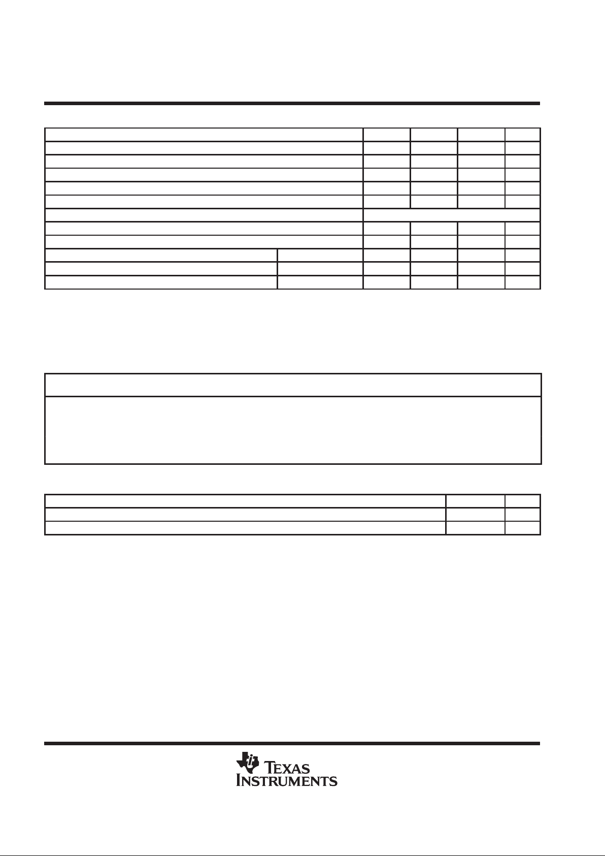
AVAILABLE OPTIONS
PACKAGE
T
A
VIOmax
AT 25°C
SMALL
OUTLINE
(D)
CHIP
CARRIER
(FK)
CERAMIC
DIP
(J)
PLASTIC
DIP
(N)
TSSOP
(PW)
0°C to 70°C 6 mV LM348D — — LM348N LM348PW
–25°C to 85°C 6 mV LM248D — — LM248N —
–55°C to 125°C 5 mV — LM148FK LM148J — —
The D package is available taped and reeled. Add the suffix R to the device type (e.g., LM348DR).
Please be aware that an important notice concerning availability, standard warranty, and use in critical applications of
Texas Instruments semiconductor products and disclaimers thereto appears at the end of this data sheet.
Copyright 1996, Texas Instruments Incorporated
PRODUCTION DATA information is current as of publication date.
Products conform to specifications per the terms of Texas Instruments
standard warranty. Production processing does not necessarily include
testing of all parameters.
1
2
3
4
5
6
7
14
13
12
11
10
9
8
1OUT
1IN–
1 IN+
V
CC+
2IN +
2IN–
2OUT
4OUT
4IN–
4IN+
V
CC –
3IN+
3IN–
3OUT
LM148 ...J PACKAGE
LM248, LM348 . . . D, N, OR PW PACKAGE
(TOP VIEW)
3 2 1 20 19
910111213
4
5
6
7
8
18
17
16
15
14
4IN+
NC
V
CC –
NC
3IN+
1IN+
NC
V
CC+
NC
2IN+
LM148 . . . FK PACKAGE
(TOP VIEW)
1IN –
1OUT
NC
3IN –
4IN –
2IN –
2OUT
NC
NC – No internal connection
3OUT
4OUT
LM148, LM248, LM348
QUADRUPLE OPERATIONAL AMPLIFIERS
SLOS058B – OCTOBER 1979 – REVISED AUGUST 1996
2
POST OFFICE BOX 655303 • DALLAS, TEXAS 75265
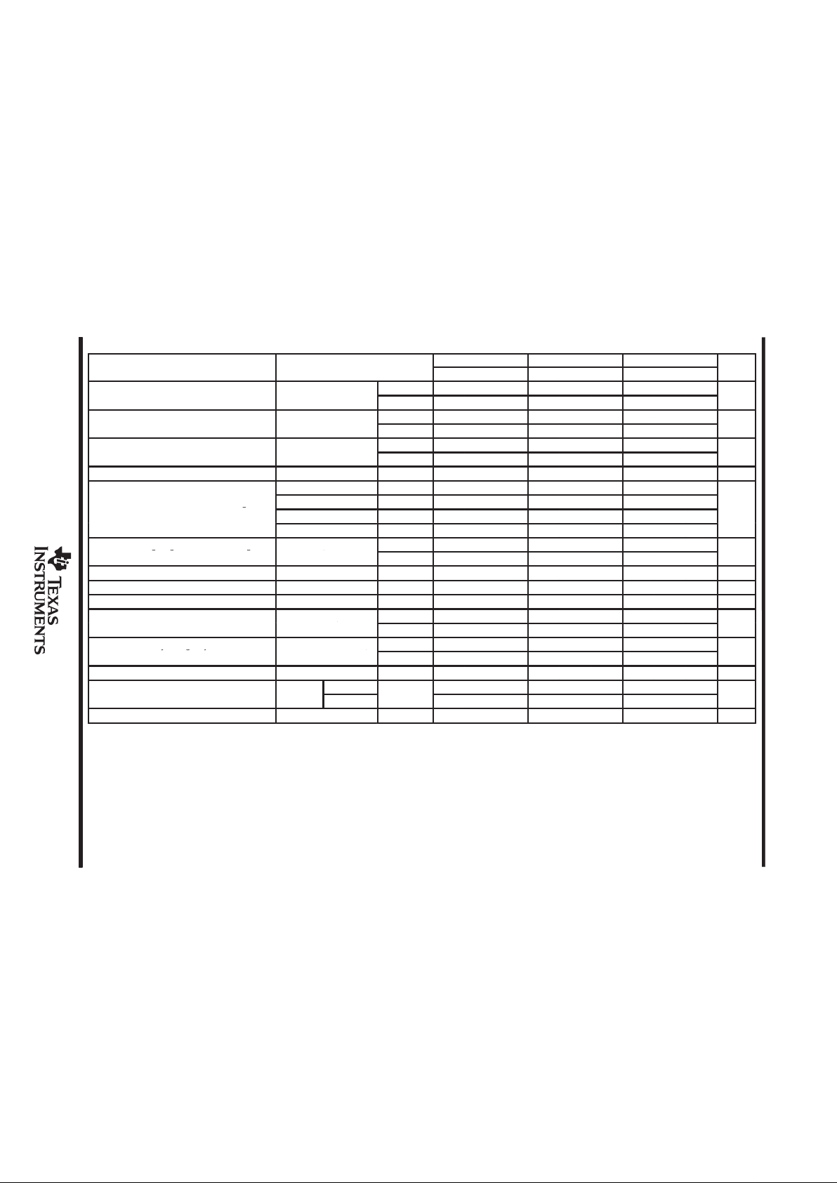
absolute maximum ratings over operating free-air temperature range (unless otherwise noted)
LM148 LM248 LM348 UNIT
Supply voltage, V
CC+
(see Note 1) 22 18 18 V
Supply voltage, V
CC–
(see Note 1) –22 –18 –18 V
Differential input voltage, VID (see Note 2) 44 36 36 V
Input voltage, VI (either input, see Notes 1 and 3) ±22 ±18 ±18 V
Duration of output short circuit (see Note 4) unlimited unlimited unlimited
Continuous total power dissipation See Dissipation Rating Table
Operating free-air temperature range, T
A
–55 to 125 –25 to 85 0 to 70 °C
Storage temperature range –65 to 150 –65 to 150 –65 to 150 °C
Case temperature for 60 seconds FK package 260 °C
Lead temperature 1,6 mm (1/16 inch) from case for 60 seconds J package 300 °C
Lead temperature 1,6 mm (1/16 inch) from case for 10 seconds D, N, or PW package 260 260 °C
NOTES: 1. All voltage values, except differential voltages, are with respect to the midpoint between V
CC+
and V
CC–
.
2. Differential voltages are at IN+ with respect to IN–.
3. The magnitude of the input voltage must never exceed the magnitude of the supply voltage or the value specified in the table,
whichever is less.
4. The output may be shorted to ground or either power supply. Temperature and/or supply voltages must be limited to ensure that
the dissipation rating is not exceeded.
DISSIPATION RATING TABLE
PACKAGE
TA ≤ 25°C
POWER RATING
DERATING
FACTOR
DERATE
ABOVE T
A
TA = 70°C
POWER RATING
TA = 85°C
POWER RATING
TA = 125°C
POWER RATING
D 900 mW 7.6 mW/°C 32°C 611 mW 497 mW N/A
FK 900 mW 11.0 mW/°C68°C 878 mW 713 mW 273 mW
J 900 mW 11.0 mW/°C68°C 878 mW 713 mW 273 mW
N 900 mW 9.2 mW/°C52°C 734 mW 596 mW N/A
PW 700 mW 5.6 mW/°C N/A 448 mW N/A N/A
recommended operating conditions
MIN MAX UNIT
Supply voltage, V
CC+
4 18 V
Supply voltage, V
CC–
–4 –18 V
LM148, LM248, LM348
QUADRUPLE OPERATIONAL AMPLIFIERS
SLOS058B – OCTOBER 1979 – REVISED AUGUST 1996
POST OFFICE BOX 655303 DALLAS, TEXAS 75265
• 3
electrical characteristics at specified free-air temperature, V
CC
±
=
±15 V (unless otherwise noted)
LM148 LM248 LM348
PARAMETER
TEST CONDITIONS
†
MIN TYP MAX MIN TYP MAX MIN TYP MAX
UNIT
p
25°C 1 5 1 6 1 6
VIOInput offset voltage
V
O
=
0
Full range 6 7.5 7.5
mV
p
25°C 4 25 4 50 4 50
IIOInput offset current
V
O
=
0
Full range 75 125 100
nA
p
25°C 30 100 30 200 30 200
IIBInput bias current
V
O
=
0
Full range 325 500 400
nA
V
ICR
Common-mode input voltage range Full range ±12 ±12 ± 12 V
RL = 10 kΩ 25°C ±12 ±13 ±12 ±13 ±12 ±13
Maximum peak output voltage
RL ≥ 10 kΩ
Full range ±12 ±12 ± 12
V
OM
g
swing
RL = 2 kΩ
25°C ±10 ±12 ±10 ± 12 ±10 ± 12
V
RL ≥ 2 kΩ Full range ±10 ±10 ± 10
Large-signal differential voltage V
= ±10 V,
25°C 50 160 25 160 25 160
A
VD
gg g
amplification
O
,
RL= ≥ 2 kΩ
Full range 25 15 15
V/mV
r
i
Input resistance
‡
25°C 0.8 2.5 0.8 2.5 0.8 2.5 MΩ
B
1
Unity-gain bandwidth AVD = 1 25°C 1 1 1 MHz
φ
m
Phase margin AVD = 1 25°C 60° 60° 60°
V
= V
min,
25°C 70 90 70 90 70 90
CMRR
Common-mode rejection ratio
IC ICR
,
VO = 0
Full range 70 70 70
dB
Supply-voltage rejection ratio V
= ± 9 V to ± 15 V,
25°C 77 96 77 96 77 96
k
SVR
ygj
(∆V
CC±
/∆VIO)
CC±
,
VO = 0
Full range 77 77 77
dB
I
OS
Short-circuit output current 25°C ±25 ±25 ±25 mA
pp
p
VO = 0
°
2.4 4.5 2.4 4.5
ICCSupply current (four amplifiers)
No load
VO = V
OM
25°C
2.4 3.6
mA
VO1/VO2Crosstalk attenuation f = 1 Hz to 20 kHz 25°C 120 120 120 dB
†
All characteristics are measured under open-loop conditions with zero common-mode input voltage unless otherwise specified. Full range for TA is – 55°C to 125°C for
LM148, –25°C to 85°C for LM248, and 0°C to 70°C for LM348.
‡
This parameter is not production tested.

LM148, LM248, LM348
QUADRUPLE OPERATIONAL AMPLIFIERS
SLOS058B – OCTOBER 1979 – REVISED AUGUST 1996
4
POST OFFICE BOX 655303 • DALLAS, TEXAS 75265
operating characteristics, V
CC
±
=
±15 V, T
A
= 25°C
PARAMETER TEST CONDITIONS MIN TYP MAX UNIT
SR Slew rate at unity gain RL = 2 kΩ, CL = 100 pF, See Figure 1 0.5 V/µs
PARAMETER MEASUREMENT INFORMATION
–
+
V
I
CL = 100 pF
RL = 2 kΩ
Figure 1. Unity-Gain Amplifier
–
+
10 kΩ
100 Ω
V
I
RL = 2 kΩ
CL = 100 pF
AVD = –100
Figure 2. Inverting Amplifier

IMPORTANT NOTICE
T exas Instruments and its subsidiaries (TI) reserve the right to make changes to their products or to discontinue
any product or service without notice, and advise customers to obtain the latest version of relevant information
to verify, before placing orders, that information being relied on is current and complete. All products are sold
subject to the terms and conditions of sale supplied at the time of order acknowledgement, including those
pertaining to warranty, patent infringement, and limitation of liability.
TI warrants performance of its semiconductor products to the specifications applicable at the time of sale in
accordance with TI’s standard warranty. Testing and other quality control techniques are utilized to the extent
TI deems necessary to support this warranty. Specific testing of all parameters of each device is not necessarily
performed, except those mandated by government requirements.
CERT AIN APPLICATIONS USING SEMICONDUCTOR PRODUCTS MAY INVOLVE POTENTIAL RISKS OF
DEATH, PERSONAL INJURY, OR SEVERE PROPERTY OR ENVIRONMENTAL DAMAGE (“CRITICAL
APPLICATIONS”). TI SEMICONDUCTOR PRODUCTS ARE NOT DESIGNED, AUTHORIZED, OR
WARRANTED TO BE SUITABLE FOR USE IN LIFE-SUPPORT DEVICES OR SYSTEMS OR OTHER
CRITICAL APPLICATIONS. INCLUSION OF TI PRODUCTS IN SUCH APPLICA TIONS IS UNDERST OOD TO
BE FULLY AT THE CUSTOMER’S RISK.
In order to minimize risks associated with the customer’s applications, adequate design and operating
safeguards must be provided by the customer to minimize inherent or procedural hazards.
TI assumes no liability for applications assistance or customer product design. TI does not warrant or represent
that any license, either express or implied, is granted under any patent right, copyright, mask work right, or other
intellectual property right of TI covering or relating to any combination, machine, or process in which such
semiconductor products or services might be or are used. TI’s publication of information regarding any third
party’s products or services does not constitute TI’s approval, warranty or endorsement thereof.
Copyright 1998, Texas Instruments Incorporated
 Loading...