

ISENSE
ADJ
VIN
PGATE
FB
EN
LM3489
GND
PGND
1
2
3
4
5
6
7
8
+ +
Q1
V
IN
V
OUT
C
IN1
C
OUT
D1
L
R
ADJ
R
IS
C
ADJ
R1
R2
C
ff
C
IN2
www.ti.com
Hysteretic PFET Buck Controller With Enable Pin
Check for Samples: LM3489, LM3489-Q1
1
FEATURES
2
• Easy to use control methodology
• No control loop compensation required
• Wide 4.5V to 35V input range
• 1.239V to VINadjustable output range
• High efficiency 93%
• ±1.3% (±2% over temp) internal reference
• 100% duty cycle operation
• Maximum operation frequency > 1MHz
• Current limit protection
• Dedicated enable pin (on if unconnected)
• Shutdown mode draws only 7µA supply
current
• VSSOP-8
• LM3489 is AEC-Q100 Grade 1 qualified
APPLICATIONS
• Set-Top Box
• DSL or Cable Modem
• PC/IA
• Auto PC
• TFT Monitor
• Battery Powered Portable Applications
• Distributed Power Systems
• Always On Power
• High Power LED Driver
• Automotive
LM3489
LM3489-Q1
SNVS443B –MAY 2006–REVISED FEBRUARY 2013
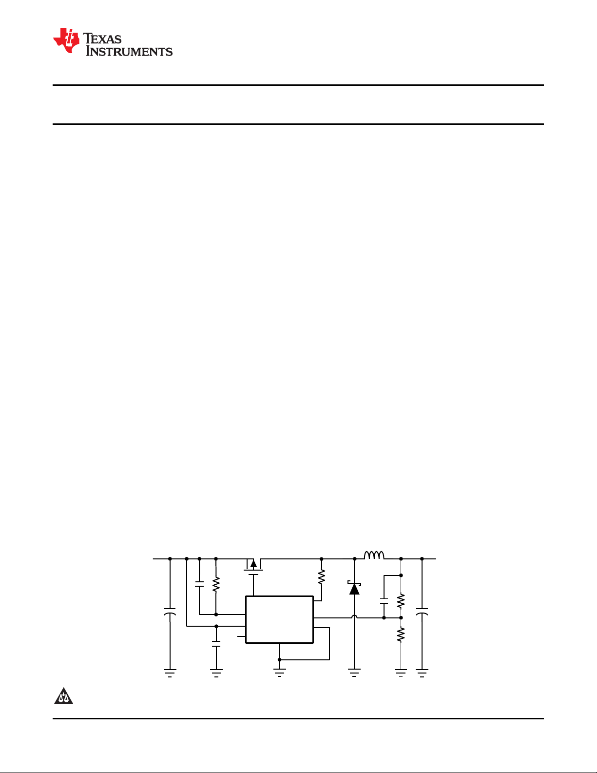
DESCRIPTION
The LM3489 is a high efficiency PFET switching
regulator controller that can be used to quickly and
easily develop a small, cost effective, switching buck
regulator for a wide range of applications. The
hysteretic control architecture provides for simple
design without any control loop stability concerns
using a wide variety of external components. The
PFET architecture also allows for low component
count as well as ultra-low dropout, 100% duty cycle
operation. Another benefit is high efficiency operation
at light loads without an increase in output ripple. A
dedicated Enable Pin provides a shutdown mode
drawing only 7µA. Leaving the Enable Pin
unconnected defaults to on.
Current limit protection can be implemented by
measuring the voltage across the PFET’s R
thus eliminating the need for a sense resistor. A
sense resistor may be used to improve current limit
accuracy if desired. The cycle-by-cycle current limit
can be adjusted with a single resistor, ensuring safe
operation over a range of output currents.
DS(ON)
,
TYPICAL APPLICATION CIRCUIT
1
2All trademarks are the property of their respective owners.
PRODUCTION DATA information is current as of publication date.
Products conform to specifications per the terms of the Texas
Instruments standard warranty. Production processing does not
necessarily include testing of all parameters.
Please be aware that an important notice concerning availability, standard warranty, and use in critical applications of
Texas Instruments semiconductor products and disclaimers thereto appears at the end of this data sheet.
Copyright © 2006–2013, Texas Instruments Incorporated
ISENSE
GND
PGND
VIN
PGATE
ADJFB
EN
1
2
3
4 5
6
7
8
LM3489
LM3489-Q1
SNVS443B –MAY 2006–REVISED FEBRUARY 2013
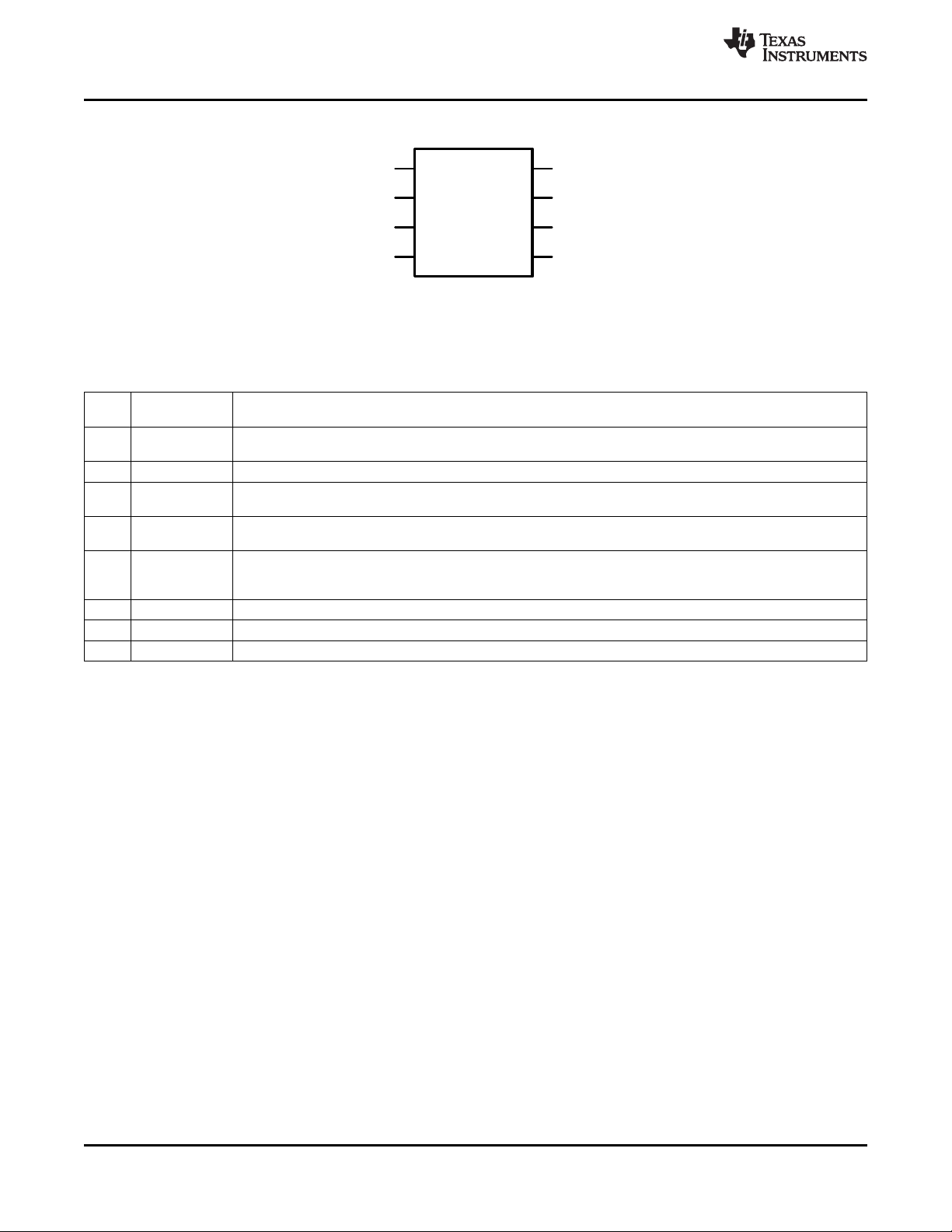
CONNECTION DIAGRAM
Figure 1. Top View
8-Lead Plastic VSSOP-8
Package Number (DGK)
PIN DESCRIPTIONS
Pin Name Description
No.
1 ISENSE The current sense input pin. This pin should be connected to the PFET drain terminal directly or through a series
resistor up to 600 ohm for 28V>Vin>35V.
2 GND Signal ground.
3 EN Enable pin. Connect EN pin to ground to shutdown the part or float to enable operation (Internally pulled high).
This pin can also be used to perform UVLO function.
4 FB The feedback input. Connect the FB to a resistor voltage divider between the output and GND for an adjustable
output voltage.
5 ADJ Current limit threshold adjustment. Connected to an internal 5.5µA current source. A resistor is connected
between this pin and VIN. The voltage across this resistor is compared with the ISENSE pin voltage to determine
if an over-current condition has occurred.
6 PGND Power ground.
7 PGATE Gate Drive output for the external PFET. PGATE swings between VIN and VIN-5V.
8 VIN Power supply input pin.
www.ti.com
2 Submit Documentation Feedback Copyright © 2006–2013, Texas Instruments Incorporated
Product Folder Links: LM3489 LM3489-Q1
www.ti.com
LM3489
LM3489-Q1
SNVS443B –MAY 2006–REVISED FEBRUARY 2013
These devices have limited built-in ESD protection. The leads should be shorted together or the device placed in conductive foam
during storage or handling to prevent electrostatic damage to the MOS gates.
Absolute Maximum Ratings
(1)
VIN Voltage −0.3V to 36V
PGATE Voltage −0.3V to 36V
FB Voltage −0.3V to 5V
ISENSE Voltage
−1.0V to 36V
-1V (<100ns)
ADJ Voltage −0.3V to 36V
EN Voltage
(2)
−0.3V to 6V
Maximum Junction Temperature 150°C
Power Dissipation, TA= 25°C
ESD Susceptibility Human Body Model
(3)
(4)
417mW
2kV
Lead Temperature Vapor Phase (60 sec.) 215°C
Infrared (15 sec.) 220°C
Storage Temperature −65°C to 150°C
(1) Absolute maximum ratings are limits beyond which damage to the device may occur. Operating Ratings are conditions for which the
device is intended to be functional, but device parameter specifications may not be ensured. For specifications and test conditions, see
the Electrical Characteristics.
(2) This pin is internally pulled high and clamped at 8V typical. The absolute maximum and operating maximum rating specifies the input
level allowed for an external voltage source applied to this pin without triggering the internal clamp with margin.
(3) The maximum allowable power dissipation is a function of the maximum junction temperature, T
resistance, θJA= 240°C/W, and the ambient temperature, TA. The maximum allowable power dissipation at any ambient temperature is
calculated using: P
(4) The human body model is a 100 pF capacitor discharged through a 1.5kΩ resistor into each pin. The machine model is a 200pF
D_MAX
= (T
- TA)/θJA. Exceeding the maximum allowable power dissipation will cause excessive die temperature.
J_MAX
, the junction-to-ambient thermal
J_MAX
capacitor discharged directly into each pin. MIL-STD-883 3015.7
Operating Ratings
(1)
Supply Voltage Range (VIN) 4.5V to 35V
EN Voltage (maximum)
(2)
5.5V
Operating Junction Temperature (TJ) −40°C to +125°C
(1) Absolute maximum ratings are limits beyond which damage to the device may occur. Operating Ratings are conditions for which the
device is intended to be functional, but device parameter specifications may not be ensured. For specifications and test conditions, see
the Electrical Characteristics.
(2) This pin is internally pulled high and clamped at 8V typical. The absolute maximum and operating maximum rating specifies the input
level allowed for an external voltage source applied to this pin without triggering the internal clamp with margin.
Copyright © 2006–2013, Texas Instruments Incorporated Submit Documentation Feedback 3
Product Folder Links: LM3489 LM3489-Q1
LM3489
LM3489-Q1
SNVS443B –MAY 2006–REVISED FEBRUARY 2013
Electrical Characteristics
(1)(2)
Specifications in Standard type face are for TJ= 25°C, and in bold type face apply over the full Operating Temperature
Range (TJ= −40°C to +125°C). Unless otherwise specified, VIN= 12V, V
= VIN− 1V, and V
ISNS
= VIN− 1.1V. Datasheet
ADJ
min/max specification limits are specified by design, test, or statistical analysis.
Symbol Parameter Test Conditions Min Typ Max Unit
I
SHDN
V
EN
V
EN_HYST
I
Q
V
FB
(3)
V
HYST
V
CL_OFFSET
I
CL_ADJ
T
CL
R
PGATE
I
PGATE
(4)
I
FB
T
ONMIN_NOR
T
ONMIN_CL
%VFB/ΔV
Shutdown input supply current EN = 0V 7 15 µA
Enable threshold voltage Enable rising 1.15 1.5 1.85 V
Enable threshold hysteresis 130 mV
Quiescent Current at ground pin FB = 1.5V (Not Switching) 280 400 µA
Feedback Voltage 1.223 1.239 1.255 V
1.214 1.264
Comparator Hysteresis 10 15 mV
14 20
Current limit comparator offset VFB= 1.0V -20 0 +20 mV
Current limit ADJ current source VFB= 1.5V 3.0 5.5 7.0 µA
Current limit one shot off time V
= 11.5V 6 9 14 µs
ADJ
V
= 11.0V
ISNS
VFB= 1.0V
Driver resistance Source 5.5 Ω
I
SOURCE
= 100mA
Sink 8.5
I
= 100mA
SINK
Driver Output current Source 0.44 A
VIN= 7V, PGATE = 3.5V
Sink 0.1
VIN = 7V, PGATE = 3.5V
FB pin Bias Current VFB= 1.0V 300 750 nA
Minimum on time in normal V
operation C
Minimum on time in current limit V
Feedback Voltage Line Regulation 4.5 ≤ VIN≤ 35V 0.01 %/V
IN
= V
ISNS
ADJ
on OUT = 1000pF
load
= V
ISNS
VFB= 1.0V
C
ADJ
on OUT = 1000pF
load
+ 0.1V 100 ns
(5)
- 0.1V 200 ns
(5)
www.ti.com
(1) All limits are specified at room temperature (standard type face) and at temperature extremes (bold type face). All room temperature
limits are 100% tested. All limits at temperature extremes are specified via correlation using standard Statistical Quality Control (SQC)
methods. All limits are used to calculate Average Outgoing Quality Level (AOQL).
(2) Typical numbers are at 25°C and represent the most likely norm.
(3) The VFBis the trip voltage at the FB pin when PGATE switches from high to low.
(4) Bias current flows out from the FB pin.
(5) A 1000pF capacitor is connected between VINand PGATE.
4 Submit Documentation Feedback Copyright © 2006–2013, Texas Instruments Incorporated
Product Folder Links: LM3489 LM3489-Q1
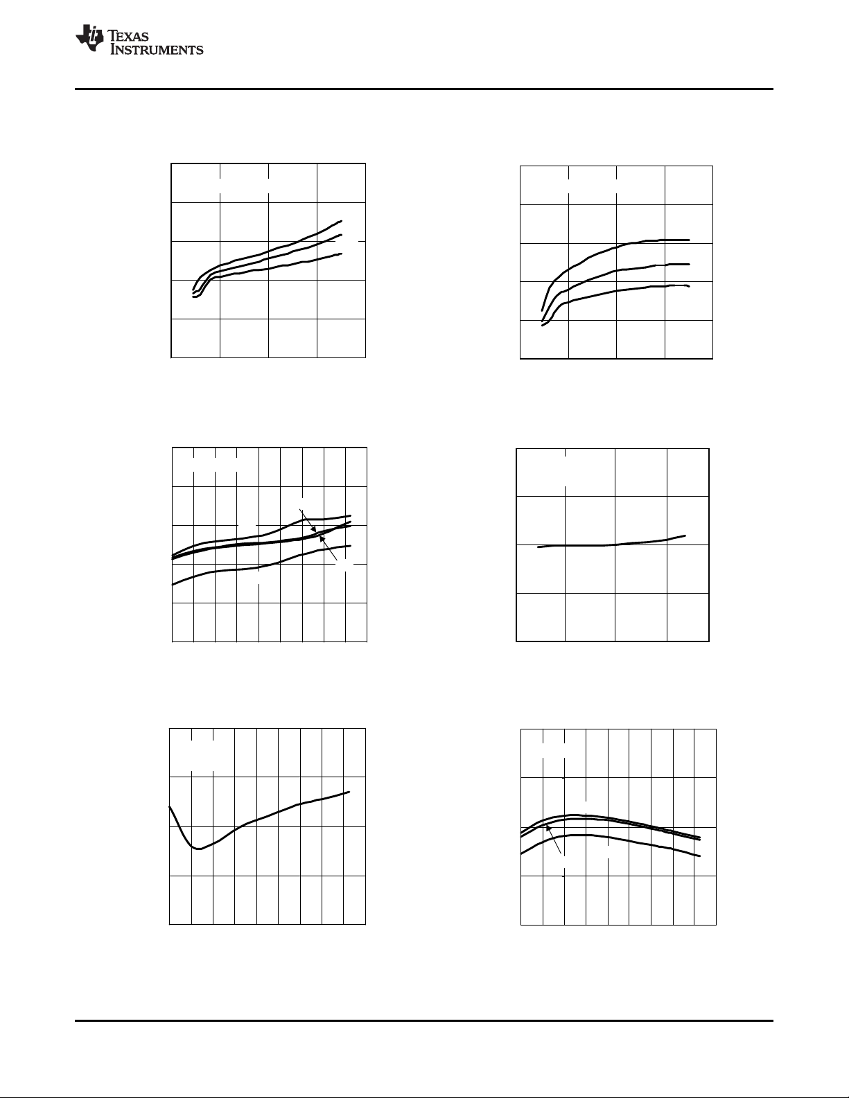
-40
-20 0 20 40 60 80 100 140
JUNCTION TEMPERATURE (°C)
120
2
6
10
14
18
V
HYST
(mV)
I
OUT
= 0
VIN = 12V
-40
-20 0 20 40 60 80 100 140
JUNCTION TEMPERATURE (°C)
120
4.5
5
5.5
6
6.5
I
CL_ADJ
(PA)
VFB = 1.5V
4.5V
18V
35V
1.214
1.224
1.234
1.244
1.254
1.264
-40
-20 0 20 40 60 80 100 140
JUNCTION TEMPERATURE (°C)
V
FB
(V)
120
I
OUT
= 200 mA
18V
35V
12V
4.5V
0 10 20 30 40
2
6
10
14
16
V
HYST
(mV)
VIN (V)
I
OUT
= 0
TJ = 25°C
0 10 20 30 40
0
3
6
9
12
15
I
IN
(PA)
VIN (V)
VFB = 1.5V, VEN = 5.5V
-40°C
25°C
125°C
0 10 20 30 40
0
100
200
300
400
500
I
IN
(
P
A
)
VIN (V)
VFB = 1.5V, VEN = 5.5V
-40°C
25°C
125°C
www.ti.com
LM3489
LM3489-Q1
SNVS443B –MAY 2006–REVISED FEBRUARY 2013
Typical Performance Characteristics
All curves taken at VIN = 12V with configuration in Design Information. TJ= 25°C, unless otherwise specified.
Quiescent Current vs Input Voltage Shutdown Current vs Input Voltage
Figure 2. Figure 3.
Feedback Voltage vs Temperature Feedback Voltage Hysteresis vs Input Voltage
Feedback Voltage Hysteresis vs Temperature Current Limit ADJ Current vs Temperature
Copyright © 2006–2013, Texas Instruments Incorporated Submit Documentation Feedback 5
Figure 4. Figure 5.
Figure 6. Figure 7.
Product Folder Links: LM3489 LM3489-Q1
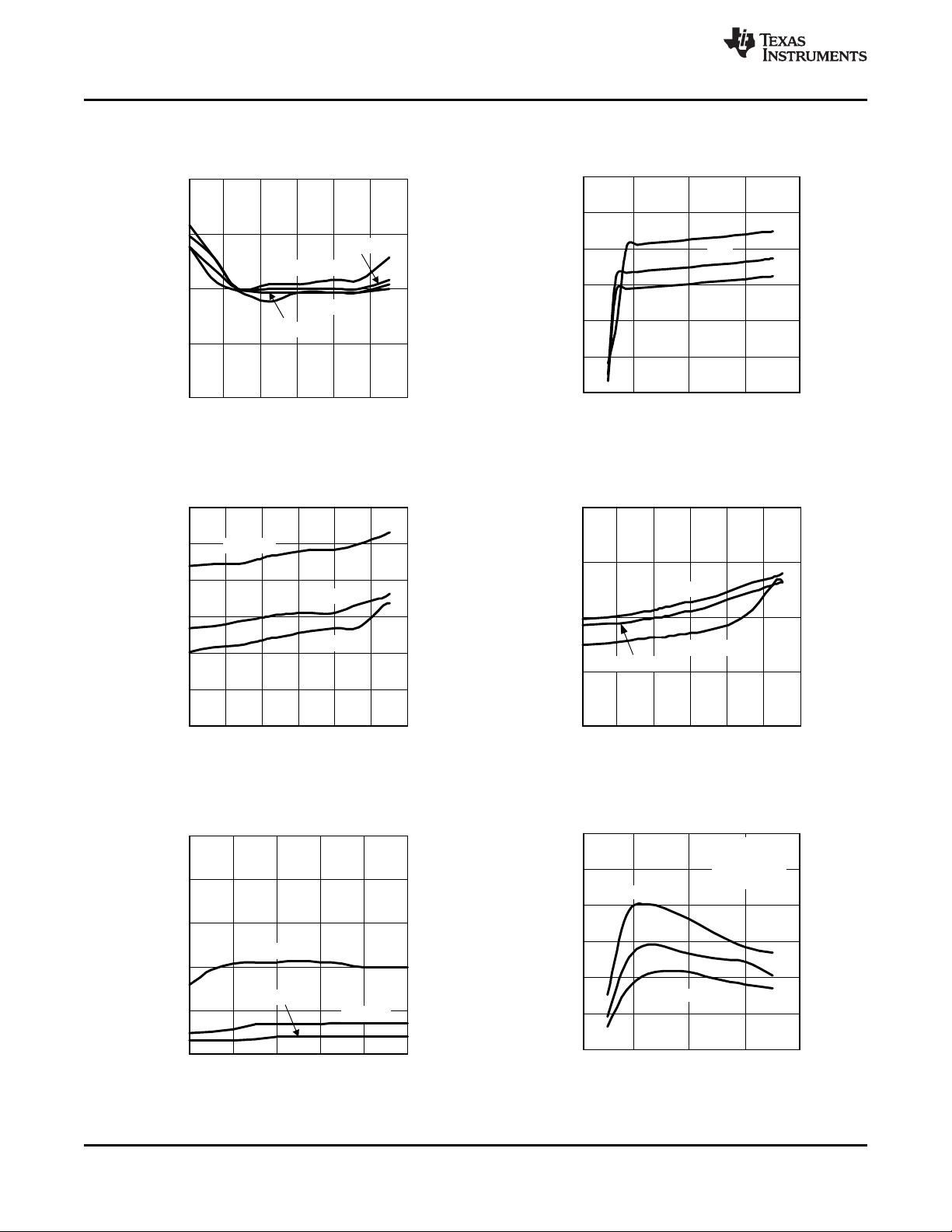
0 0.2 0.4 0.6 0.8 1
0
2
4
6
8
10
OPERATING ON TIME (Ps)
LOAD CURRENT (A)
VIN = 12V
VIN = 6V
VIN = 24V
0 40
0
100
200
300
400
500
600
OPERATING FREQUENCY (kHz)
VIN (V)
10 20 30
L = 10 PH
L = 15 PH
L = 22 PH
V
OUT
= 3.3V
I
OUT
= 500 mA
Cff = 100 pF
-40 -10 20 50 80 110 140
JUNCTION TEMPERATURE, TJ (°C)
40
60
80
100
120
140
160
T
ONMIN_NOR
(ns)
VIN = 4.5V
VIN = 24V
VIN = 12V
-40 -10 20 50 80 110 140
JUNCTION TEMPERATURE, TJ (oC)
100
150
200
250
300
T
ONMIN_CL
(ns)
VIN = 12V
VIN = 4.5V
VIN = 24V
-40 -10 20 50 80 110 140
JUNCTION TEMPERATURE, TJ (°C)
8
8.5
9
9.5
10
T
CL
(Ps)
VIN = 12V
VIN = 4.5V
VIN = 24V
VIN = 35V
0 40
3
3.5
4
4.5
5
5.5
6
V
IN
-V
PGATE
(V)
VIN (V)
10 20 30
-40°C
25°C
125°C
LM3489
LM3489-Q1
SNVS443B –MAY 2006–REVISED FEBRUARY 2013
Typical Performance Characteristics (continued)
All curves taken at VIN = 12V with configuration in Design Information. TJ= 25°C, unless otherwise specified.
Current Limit One Shot OFF Time vs Temperature VIN- V
Figure 8. Figure 9.
Minimum ON Time vs Temperature (Normal Operation) Minimum ON Time vs Temperature (Current Limit)
PGATE
vs V
IN
www.ti.com
Operating ON Time vs Load Current Operating Frequency vs Input Voltage
6 Submit Documentation Feedback Copyright © 2006–2013, Texas Instruments Incorporated
Figure 10. Figure 11.
Figure 12. Figure 13.
Product Folder Links: LM3489 LM3489-Q1
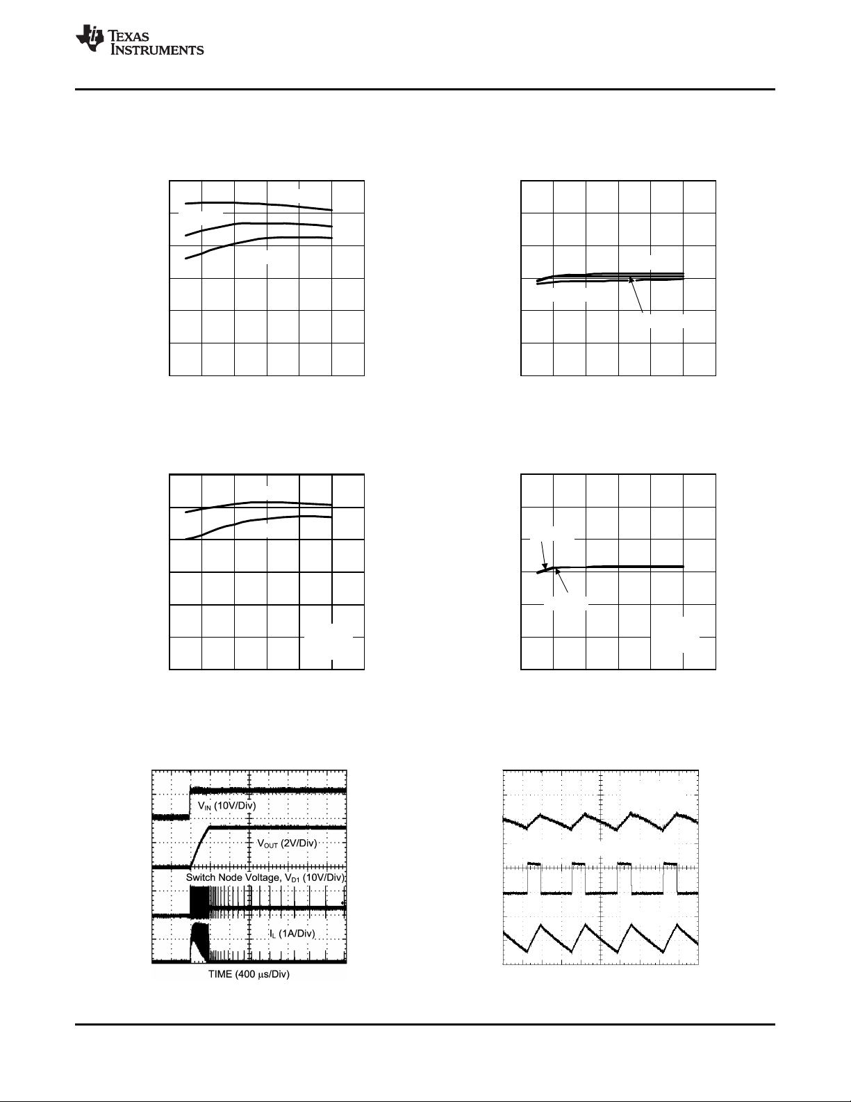
V
OUT
RIPPLE
(50 mVac/Div)
Switch Node Voltage, VD1 (10V/Div)
IL (1A/Div)
TIME (2 Ps/DIV)
0.0 0.2 0.4 0.6 0.8 1.0 1.2
OUTPUT CURRENT (A)
40
50
60
70
80
90
100
EFFICIENCY (%)
L = 22 PH
R1 = 60.7k
R2 = 20k
VIN = 24V
VIN = 12V
0.0 0.2 0.4 0.6 0.8 1.0 1.2
OUTPUT CURRENT (A)
-3.0
-2.0
-1.0
0.0
1.0
2.0
3.0
'V
OUT
(%)
VIN = 24V
VIN = 12V
L = 22 PH
R1 = 60.7k
R2 = 20k
0.0 0.2 0.4 0.6 0.8 1.0 1.2
OUTPUT CURRENT (A)
40
50
60
70
80
90
100
EFFICIENCY (%)
VIN = 4.5V
VIN = 24V
VIN = 12V
0.0 0.2 0.4 0.6 0.8 1.0 1.2
OUTPUT CURRENT (A)
-3.0
-2.0
-1.0
0.0
1.0
2.0
3.0
'V
OUT
(%)
VIN = 4.5V
VIN = 24V
VIN = 12V
www.ti.com
SNVS443B –MAY 2006–REVISED FEBRUARY 2013
Typical Performance Characteristics (continued)
All curves taken at VIN = 12V with configuration in Design Information. TJ= 25°C, unless otherwise specified.
LM3489
LM3489-Q1
Efficiency vs Load Current V
(V
= 3.3V, L = 22µH) (V
OUT
Figure 14. Figure 15.
Efficiency vs Load Current (V
= 5V, L = 22µH) V
OUT
Regulation vs Load Current
OUT
Regulation vs Load Current (V
OUT
= 3.3V, L = 22µH)
OUT
= 5V, L = 22µH)
OUT
Copyright © 2006–2013, Texas Instruments Incorporated Submit Documentation Feedback 7
Figure 16. Figure 17.
Power Up (No Load, C
Figure 18. Figure 19.
= 1nF) (VIN= 12V, V
ADJ
Product Folder Links: LM3489 LM3489-Q1
Continuous Mode Operation
OUT
= 3.3 V, I
OUT
= 500mA)
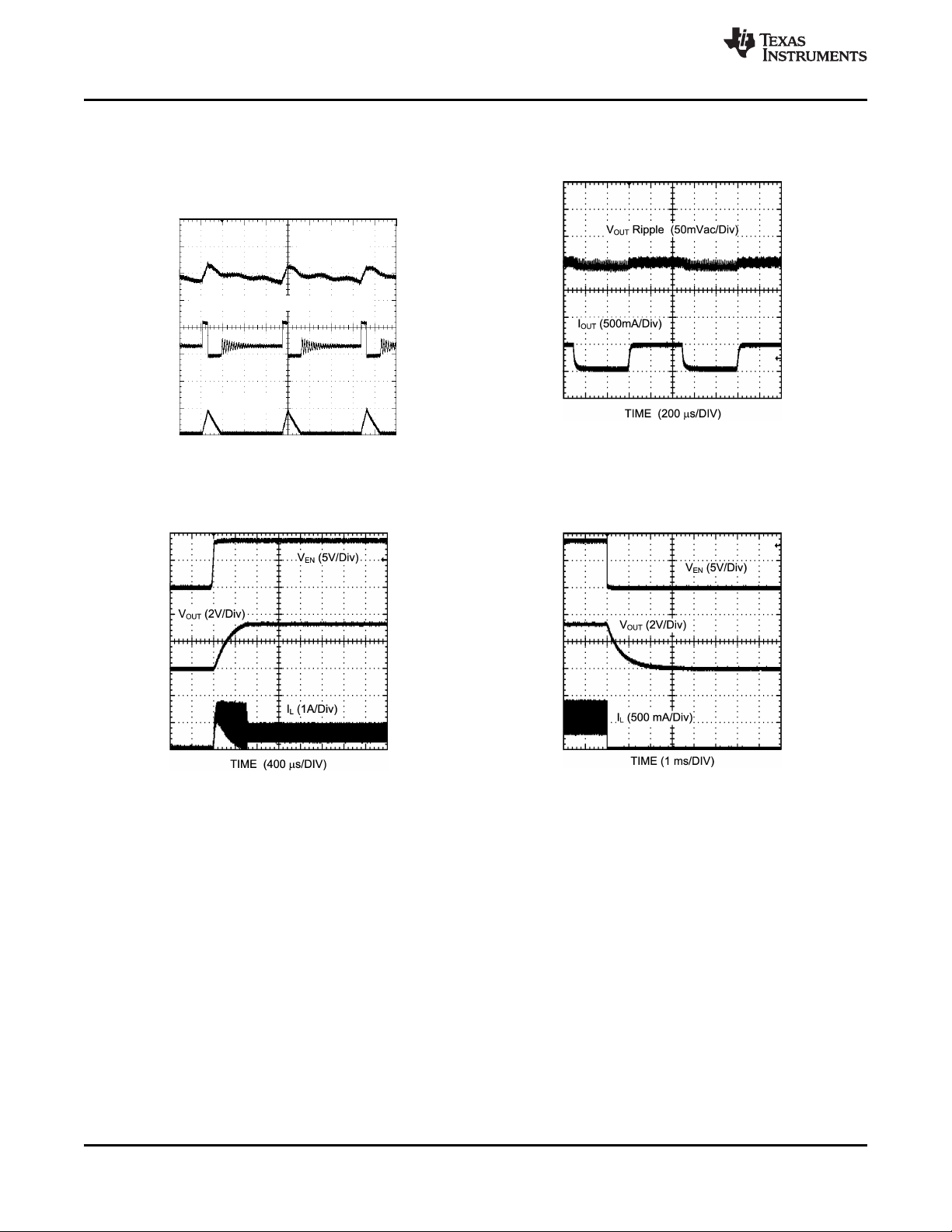
V
OUT
RIPPLE
(20 mVac/Div)
Switch Node Voltage, VD1 (10V/Div)
IL (500 mA/Div)
TIME (4 Ps/DIV)
LM3489
LM3489-Q1
SNVS443B –MAY 2006–REVISED FEBRUARY 2013
Typical Performance Characteristics (continued)
All curves taken at VIN = 12V with configuration in Design Information. TJ= 25°C, unless otherwise specified.
Discontinuous Mode Operation Load Transient
(VIN= 12V, V
OUT
=3.3 V, I
= 50mA) (V
OUT
= 3.3 V, 50 mA - 500 mA Load)
OUT
Figure 20. Figure 21.
www.ti.com
Enable Transient Shutdown Transient
(V
= 3.3 V, 500 mA Loaded) (V
OUT
= 3.3 V, 500 mA Loaded)
OUT
Figure 22. Figure 23.
8 Submit Documentation Feedback Copyright © 2006–2013, Texas Instruments Incorporated
Product Folder Links: LM3489 LM3489-Q1

www.ti.com
LM3489
LM3489-Q1
SNVS443B –MAY 2006–REVISED FEBRUARY 2013
SIMPLIFIED FUNCTIONAL BLOCK DIAGRAM
FUNCTIONAL DESCRIPTION
OVERVIEW
The LM3489 is a buck (step-down) DC-DC controller that uses a hysteretic control scheme. The control
comparator is designed with approximately 10mV of hysteresis. In response to the voltage at the FB pin, the gate
drive (PGATE pin) turns the external PFET on or off. When the inductor current is too high, the current limit
protection circuit engages and turns the PFET off for approximately 9µs.
Hysteretic control does not require an internal oscillator. Switching frequency depends on the external
components and operating conditions. The operating frequency reduces at light loads resulting in excellent
efficiency compared to other architectures.
The output voltage can be programmed by two external resistors. The output can be set in a wide range from
1.239V (typical) to VIN.
HYSTERETIC CONTROL CIRCUIT
When the FB input to the control comparator falls below the reference voltage (1.239V), the output of the
comparator switches to a low state. This results in the driver output, PGATE, pulling the gate of the PFET low
and turning on the PFET. With the PFET on, the input supply charges C
the series path through the PFET and the inductor. Current through the Inductor ramps up linearly and the output
voltage increases. As the FB voltage reaches the upper threshold, which is the internal reference voltage plus
10mV, the output of the comparator changes from low to high, and the PGATE responds by turning the PFET off.
As the PFET turns off, the inductor voltage reverses, the catch diode turns on, and the current through the
inductor ramps down. Then, as the output voltage reaches the internal reference voltage again, the next cycle
starts.
and supplies current to the load via
OUT
Copyright © 2006–2013, Texas Instruments Incorporated Submit Documentation Feedback 9
Product Folder Links: LM3489 LM3489-Q1

LM3489
LM3489-Q1
SNVS443B –MAY 2006–REVISED FEBRUARY 2013
The LM3489 operates in discontinuous conduction mode at light load current or continuous conduction mode at
heavy load current. In discontinuous conduction mode, current through the inductor starts at zero and ramps up
to the peak, then ramps down to zero. The next cycle starts when the FB voltage reaches the reference voltage.
Until then, the inductor current remains zero and the output capacitor supplies the load. The operating frequency
is lower and switching losses reduced. In continuous conduction mode, current always flows through the inductor
and never ramps down to zero.
The output voltage (V
V
= 1.239 x (R1 + R2) / R2 (1)
OUT
) can be programmed by 2 external resistors. It can be calculated as follows:
OUT
www.ti.com
Figure 24. Hysteretic Window
The minimum output voltage ripple (V
V
For example, with V
V
= V
OUT_PP
= 0.01 x (33K + 20k) / 20k = 0.0266V (3)
OUT_PP
(R1 + R2) / R2 (2)
HYST
set to 3.3V, V
OUT
Operating frequency (F) is determined by knowing the input voltage, output voltage, inductor, V
) can be calculated in the same way.
OUT_PP
OUT_PP
is 26.6mV
HYST
, ESR
(Equivalent Series Resistance) of output capacitor, and the delay. It can be approximately calculated using the
formula:
(4)
where:
α: (R1 + R2) / R2
delay: It includes the LM3489 propagation delay time and the PFET delay time. The propagation delay is 90ns
typically (see Figure 25).
10 Submit Documentation Feedback Copyright © 2006–2013, Texas Instruments Incorporated
Product Folder Links: LM3489 LM3489-Q1

INPUT VOLTAGE - OUTPUT VOLTAGE (V)
PROPOGATION DELAY (ns)
0
20
40
60
80
100
120
140
0
5
10
15
20
25 30
35
L=10PH
L=4.7PH
L=22PH
LM3489
LM3489-Q1
www.ti.com
Figure 25. Propagation Delay
The operating frequency and output ripple voltage can also be significantly influenced by the speed up capacitor
(Cff). Cff is connected in parallel with the high side feedback resistor, R1. The location of this capacitor is similar
to where a phase lead capacitor would be located in a PWM control scheme. However it's effect on hysteretic
operation is much different. Cff effectively shorts out R1 at the switching frequency and applies the full output
ripple to the FB pin without dividing by the R2/R1 ratio. The end result is a reduction in output ripple and an
increase in operating frequency. When adding Cff, calculate the formula above with α = 1. The value of Cff
depend on the desired operating frequency and the value of R2. A good starting point is 470pF ceramic at
100kHz decreasing linearly with increased operating frequency. Also note that as the output voltage is
programmed below 2.5V, the effect of Cff will decrease significantly.
SNVS443B –MAY 2006–REVISED FEBRUARY 2013
CURRENT LIMIT OPERATION
The LM3489 has a cycle-by-cycle current limit. Current limit is sensed across the VDSof the PFET or across an
additional sense resistor. When current limit is activated, the LM3489 turns off the external PFET for a period of
9µs(typical). The current limit is adjusted by an external resistor, R
The current limit circuit is composed of the ISENSE comparator and the one-shot pulse generator. The positive
input of the ISENSE comparator is the ADJ pin. An internal 5.5µA current sink creates a voltage across the
external R
resistor. This voltage is compared to the voltage across the PFET or sense resistor. The ADJ
ADJ
voltage can be calculated as follows:
V
= VIN− (R
ADJ
Where 3.0µA is the minimum I
x 3.0µA) (5)
ADJ
value.
CL-ADJ
The negative input of the ISENSE comparator is the ISENSE pin that should be connected to the drain of the
external PFET. The inductor current is determined by sensing the VDS. It can be calculated as follows.
V
ISENSE
= VIN− (R
DSON
x I
IND_PEAK
) = VIN− V
DS
ADJ
.
(6)
Copyright © 2006–2013, Texas Instruments Incorporated Submit Documentation Feedback 11
Figure 26. Current Sensing by V
Product Folder Links: LM3489 LM3489-Q1
DS

LM3489
LM3489-Q1
SNVS443B –MAY 2006–REVISED FEBRUARY 2013
www.ti.com
The current limit is activated when the voltage at the ADJ pin exceeds the voltage at the I
pin. The ISENSE
SENSE
comparator triggers the 9µs one shot pulse generator forcing the driver to turn the PFET off. The driver turns the
PFET back on after 9µs. If the current has not reduced below the set threshold, the cycle will repeat
continuously.
A filter capacitor, C
, should be placed as shown in Figure 26. C
ADJ
filters unwanted noise so that the ISENSE
ADJ
comparator will not be accidentally triggered. A value of 100pF to 1nF is recommended in most applications.
Higher values can be used to create a soft-start function (See Start Up section).
The current limit comparator has approximately 100ns of blanking time. This ensures that the PFET is fully on
when the current is sensed. However, under extreme conditions such as cold temperature, some PFETs may not
fully turn on within the blanking time. In this case, the current limit threshold must be increased. If the current limit
function is used, the on time must be greater than 100ns. Under low duty cycle operation, the maximum
operating frequency will be limited by this minimum on time.
During current limit operation, the output voltage will drop significantly as will operating frequency. As the load
current is reduced, the output will return to the programmed voltage. However, there is a current limit fold back
phenomenon inherent in this current limit architecture. See Figure 27.
Figure 27. Current Limit Fold Back Phenomenon
At high input voltages (>28V) increased undershoot at the switch node can cause an increase in the current limit
threshold. To avoid this problem, a low Vf Schottky catch diode must be used (See Catch Diode Selection).
Additionally, a resistor can be placed between the ISENSE pin and the switch node. Any value in the range of
220Ω to 600Ω is recommended.
START UP
The current limit circuit is active during start-up. During start-up the PFET will stay on until either the current limit
or the feedback comparator is tripped
If the current limit comparator is tripped first then the fold back characteristic should be taken into account. Startup into full load may require a higher current limit set point or the load must be applied after start-up.
One problem with selecting a higher current limit is inrush current during start-up. Increasing the capacitance
(C
) in parallel with R
ADJ
results in a soft-start characteristic. C
ADJ
ADJ
and R
create an RC time constant forcing
ADJ
current limit to activate at a lower current. The output voltage will ramp more slowly when using this technique.
There is example start-up plot for C
C
will have little to no effect on soft-start.
ADJ
equal to 1nF in the Typical Performance Characteristics. Lower values for
ADJ
EXTERNAL SENSE RESISTOR
The VDSof a PFET will tend to vary significantly over temperature. This will result an equivalent variation in
current limit. To improve current limit accuracy an external sense resistor can be connected from VINto the
source of the PFET, as shown in Figure 28. The current sense resistor, RCSshould have value comparable with
R
OPERATION can be used by replacing the R
of the PFET used, typically in the range of 50mΩ to 200 mΩ. The equation in CURRENT LIMIT
DSON
DSON
with RCS.
12 Submit Documentation Feedback Copyright © 2006–2013, Texas Instruments Incorporated
Product Folder Links: LM3489 LM3489-Q1

V
IN(UVLO_HYST)
= V
EN_HYST
x
1+
R4
R3
V
IN(UVLO)
= V
EN
1 +
R4
R3
LM3489
LM3489-Q1
www.ti.com
Figure 28. Current Sensing by External Resistor
PGATE
When switching, the PGATE pin swings from VIN (off) to some voltage below VIN (on). How far the PGATE will
swing depends on several factors including the capacitance, on time, and input voltage.
PGATE voltage swing will increase with decreasing gate capacitance. Although PGATE voltage will typically be
around VIN-5V, with very small gate capacitances, this value can increase to a typical maximum of VIN-8.3V.
Additionally, PGATE swing voltage will increase as on time increases. During long on times, such as when
operating at 100% duty cycle, the PGATE voltage will eventually fall to its maximum voltage of VIN-8.3V (typical)
regardless of the PFET gate capacitance.
The PGATE voltage will not fall below 0.4V (typical). Therefore, when the input voltage falls below approximately
9V, the PGATE swing voltage range will be reduced. At an input voltage of 7V, for instance, PGATE will swing
from 7V to a minimum of 0.4V.
SNVS443B –MAY 2006–REVISED FEBRUARY 2013
DEVICE ENABLE, SHUTDOWN
The LM3489 can be remotely shutdown by forcing the enable pin to ground. With EN pin grounded, the internal
blocks other than the enable logic are de-activated and the shutdown current of the device will be lowered to only
7µA (typical). Releasing the EN pin allows for normal operation to resume. The EN pin is internally pulled high
with the voltage clamped at 8V typical. For normal operation this pin should be left open. In case an external
voltage source is applied to this pin for enable control, the applied voltage should not exceed the maximum
operating voltage level specified in this datasheet, i.e. 5.5V.
ADJUSTABLE UVLO
The under-voltage-lockout function can be implemented as shown in Figure 29. By incorporating the feature of
the internal enable threshold, the lockout level can be programmed through an external potential divider formed
with R3 and R4. The input voltage information is detected and compared with the enable threshold and the
device operation will be inhibited when VINdrops below the preset UVLO level. The UVLO and hysteresis voltage
can be calculated as follows:
(7)
(8)
where VENis the enable rising threshold voltage and V
EN_HYST
is the enable threshold hysteresis.
Copyright © 2006–2013, Texas Instruments Incorporated Submit Documentation Feedback 13
Product Folder Links: LM3489 LM3489-Q1

Ipk =
I
OUT
+
'i
2
x 1.1
Ipk =
I
OUT
+
'i
2
x 1.1
VIN - VDS - V
OUT
L =
'i
x
D
f
ISENSE
ADJ
VIN
PGATE
FB
EN
LM3489
GND
PGND
1
2
3
4
5
6
7
8
V
IN
V
EN
R3
R4
LM3489
LM3489-Q1
SNVS443B –MAY 2006–REVISED FEBRUARY 2013
Figure 29. Adjustable UVLO
DESIGN INFORMATION
Hysteretic control is a simple control scheme. However the operating frequency and other performance
characteristics highly depend on external conditions and components. If either the inductance, output
capacitance, ESR, VIN, or Cff is changed, there will be a change in the operating frequency and output ripple.
The best approach is to determine what operating frequency is desirable in the application and then begin with
the selection of the inductor and C
OUT
ESR.
www.ti.com
INDUCTOR SELECTION (L)
The important parameters for the inductor are the inductance and the current rating. The LM3489 operates over
a wide frequency range and can use a wide range of inductance values. A rule of thumb is to use the equations
used for Simple Switchers®. The equation for inductor ripple (Δi) as a function of output current (I
for I
Δi ≤ I
for I
Δi ≤ I
< 2.0Amps
out
x I
out
> 2.0Amps
out
x 0.3
out
−0.366726
out
The inductance can be calculated based upon the desired operating frequency where:
And
where D is the duty cycle, VDis the diode forward voltage, and VDSis the voltage drop across the PFET.
The inductor should be rated to the following:
The inductance value and the resulting ripple is one of the key parameters controlling operating frequency. The
second is the inductor ESR that contribute to the steady state power loss due to current flowing through the
inductor.
OUT
) is:
(9)
(10)
(11)
14 Submit Documentation Feedback Copyright © 2006–2013, Texas Instruments Incorporated
Product Folder Links: LM3489 LM3489-Q1

R
DSON
R
ADJ
= I
IND_PEAK
x
I
CL_ADJ
V
OUT(VIN
± V
OUT
)
I
RMS_CIN
= I
OUT
x
V
IN
www.ti.com
LM3489
LM3489-Q1
SNVS443B –MAY 2006–REVISED FEBRUARY 2013
OUTPUT CAPACITOR SELECTION (C
OUT
)
The ESR of the output capacitor times the inductor ripple current is equal to the output ripple of the regulator.
However, the V
sets the first order value of this ripple. As ESR is increased with a given inductance,
HYST
operating frequency increases as well. If ESR is reduced then the operating frequency reduces.
The use of ceramic capacitors has become a common desire of many power supply designers. However,
ceramic capacitors have a very low ESR resulting in a 90° phase shift of the output voltage ripple. This results in
low operating frequency and increased output ripple. To fix this problem a low value resistor should be added in
series with the ceramic output capacitor. Although counter intuitive, this combination of a ceramic capacitor and
external series resistance provides highly accurate control over the output voltage ripple. Other types capacitor,
such as Sanyo POS CAP and OS-CON, Panasonic SP CAP, and Nichicon "NA" series, are also recommended
and may be used without additional series resistance.
For all practical purposes, any type of output capacitor may be used with proper circuit verification.
INPUT CAPACITOR SELECTION (CIN)
A bypass capacitor is required between the input source and ground. It must be located near the source pin of
the external PFET. The input capacitor prevents large voltage transients at the input and provides the
instantaneous current when the PFET turns on.
The important parameters for the input capacitor are the voltage rating and the RMS current rating. Follow the
manufacturer's recommended voltage derating. For high input voltage applications, low ESR electrolytic,
Nichicon "UD" series or the Panasonic "FK" series are available. The RMS current in the input capacitor can be
calculated as follows:
(12)
The input capacitor power dissipation can be calculated as follows.
P
= I
D(CIN)
The input capacitor must be able to handle the RMS current and the dissipation. Several input capacitors may be
connected in parallel to handle large RMS currents. In some cases it may be much cheaper to use multiple
electrolytic capacitors than a single low ESR, high performance capacitor such as OS-CON or Tantalum. The
capacitance value should be selected such that the ripple voltage created by the switch current pulses is less
than 10% of the total DC voltage across the capacitor.
For high VIN conditions (> 28V), the fast switching, high swing of the internal gate drive introduces unwanted
disturbance to the VIN rail and the current limit function can be affected. In order to eliminate this potential
problem, a high quality ceramic capacitor of 0.1 µF is recommended to filter out the internal disturbance at the
VIN pin. This capacitor should be placed right next to the VIN pin for best performance.
RMS_CIN
2
x ESR
CIN
(13)
PROGRAMMING THE CURRENT LIMIT (R
The current limit is determined by connecting a resistor (R
ADJ
)
) between input voltage and the ADJ pin, pin 5.
ADJ
where:
R
I
I
Using the minimum value for I
: Drain-Source ON resistance of the external PFET
DSON
: 3.0µA minimum
CL_ADJ
IND_PEAK
= I
LOAD
+ I
RIPPLE
/2
(3.0µA) ensures that the current limit threshold will be set higher than the
CL_ADJ
peak inductor current.
The R
mind, R
PFET with a lower R
Copyright © 2006–2013, Texas Instruments Incorporated Submit Documentation Feedback 15
value must be selected to ensure that the voltage at the ADJ pin does not fall below 3.5V. With this in
ADJ
ADJ_MAX
= (VIN-3.5)/7µA. If a larger R
, or use a current sense resistor as shown in Figure 28.
DSON
value is needed to set the desired current limit, either use a
ADJ
Product Folder Links: LM3489 LM3489-Q1
(14)

LM3489
LM3489-Q1
SNVS443B –MAY 2006–REVISED FEBRUARY 2013
The current limit function can be disabled by connecting the ADJ pin to ground and ISENSE to VIN.
CATCH DIODE SELECTION (D1)
The important parameters for the catch diode are the peak current, the peak reverse voltage, and the average
power dissipation. The average current through the diode can be calculated as following.
I
= I
D_AVE
x (1 − D) (15)
OUT
The off state voltage across the catch diode is approximately equal to the input voltage. The peak reverse
voltage rating must be greater than input voltage. In nearly all cases a Schottky diode is recommended. In low
output voltage applications a low forward voltage provides improved efficiency. For high temperature
applications, diode leakage current may become significant and require a higher reverse voltage rating to
achieve acceptable performance.
P-CHANNEL MOSFET SELECTION (Q1)
The important parameters for the PFET are the maximum Drain-Source voltage (VDS), the on resistance (R
Current rating, and the input capacitance.
The voltage across the PFET when it is turned off is equal to the sum of the input voltage and the diode forward
voltage. The VDSmust be selected to provide some margin beyond the input voltage.
PFET drain current, Id, must be rated higher than the peak inductor current, I
IND-PEAK
Depending on operating conditions, the PGATE voltage may fall as low as VIN- 8.3V. Therefore, a PFET must
be selected with a VGSmaximum rating greater than the maximum PGATE swing voltage.
As input voltage decreases below 9V, PGATE swing voltage may also decrease. At 5.0V input the PGATE will
swing from VINto VIN- 4.6V. To ensure that the PFET turns on quickly and completely, a low threshold PFET
should be used when the input voltage is less than 7V.
Total power loss in the FET can be approximated using the following equation:
PD
switch
= R
DSON
x I
2
x D + F x I
OUT
x VINx (ton+ t
OUT
)/2 (16)
off
.
www.ti.com
DSON
),
where:
ton= FET turn on time
t
= FET turn off time
off
A value of 10ns to 20ns is typical for ton and toff.
A PFET should be selected with a turn on rise time of less than 100ns. Slower rise times will degrade efficiency,
can cause false current limiting, and in extreme cases may cause abnormal spiking at the PGATE pin.
The R
temperature coefficient. At 100°C, the R
increase in R
is used in determining the current limit resistor value, R
DSON
must be considered when determining R
DSON
may be as much as 150% higher than the 25°C value. This
DSON
. Note that the R
ADJ
in wide temperature range applications. If the
ADJ
has a positive
DSON
current limit is set based upon 25°C ratings, then false current limiting can occur at high temperature.
Keeping the gate capacitance below 2000pF is recommended to keep switching losses and transition times low.
This will also help keep the PFET drive current low, which will improve efficiency and lower the power dissipation
within the controller.
As gate capacitance increases, operating frequency should be reduced and as gate capacitance decreases
operating frequency can be increased.
INTERFACING WITH THE ENABLE PIN
The enable pin is internally pulled high with clamping at 8V typical. For normal operation this pin should be left
open. To disable the device, the enable pin should be connected to ground externally. If an external voltage
source is applied to this pin for enable control, the applied voltage should not exceed the maximum operating
voltage level specified in this datasheet, i.e. 5.5V. For most applications, an open drain or open collector
transistor can be used to short this pin to ground to shutdown the device .
16 Submit Documentation Feedback Copyright © 2006–2013, Texas Instruments Incorporated
Product Folder Links: LM3489 LM3489-Q1

ISENSE
ADJ
VIN
PGATE
FB
EN
LM3489
GND
PGND
7
2
3
4
5
6
1
8
+ +
Q1 FDC5614P
V
IN
V
OUT
C
IN1
C
OUT
D1
L 22 PH
R
ADJ
C
ADJ
R1
R2
C
ff
C
IN2
7V ± 35V
22 PF
50V
0.1PF
50V
3.3V/0.5A
1 nF
24k
33k
20k
100 pF
100 PF
6.3V
MBRS140
SD*
* Short to shutdown
the device
R
IS
270
LM3489
LM3489-Q1
www.ti.com
PCB Layout
The PCB board layout is very important in all switching regulator designs. Poor layout can cause switching noise
into the feedback signal and generate EMI problems. For minimal inductance, the wires indicated by heavy lines
in schematic diagram should be as wide and short as possible. Keep the ground pin of the input capacitor as
close as possible to the anode of the catch diode. This path carries a large AC current. The switching node, the
node with the diode cathode, inductor and FET drain should be kept short. This node is one of the main sources
for radiated EMI since it sees a large AC voltage at the switching frequency. It is always a good practice to use a
ground plane in the design, particularly for high current applications.
The two ground pins, PGND and GND, should be connected by as short a trace as possible. They can be
connected underneath the device. These pins are resistively connected internally by approximately 50Ω. The
ground pins should be tied to the ground plane, or to a large ground trace in close proximity to both the FB
divider and C
The gate pin of the external PFET should be located close to the PGATE pin. However, if a very small FET is
used, a resistor may be required between PGATE pin and the gate of the PFET to reduce high frequency ringing.
Since this resistor will slow down the PFET’s rise time, the current limit blanking time should be taken into
consideration (refer to Current Limiting Operation). The feedback voltage signal line can be sensitive to noise.
Avoid inductive coupling with the inductor or the switching node. The FB trace should be kept away from those
areas. Also, the orientation of the inductor can contribute un-wanted noise coupling to the FB path. If noise
problems are observed it may be worth trying a different orientation of the inductor and select the best for final
component placement.
OUT
grounds.
SNVS443B –MAY 2006–REVISED FEBRUARY 2013
Figure 30. Typical Application Schematic for VOUT = 3.3V/500mA
Copyright © 2006–2013, Texas Instruments Incorporated Submit Documentation Feedback 17
Product Folder Links: LM3489 LM3489-Q1

LM3489
LM3489-Q1
SNVS443B –MAY 2006–REVISED FEBRUARY 2013
REVISION HISTORY
Changes from Revision A (February 2013) to Revision B Page
• Changed layout of National Data Sheet to TI format .......................................................................................................... 17
www.ti.com
18 Submit Documentation Feedback Copyright © 2006–2013, Texas Instruments Incorporated
Product Folder Links: LM3489 LM3489-Q1

PACKAGE OPTION ADDENDUM
www.ti.com
22-Sep-2015
PACKAGING INFORMATION
Orderable Device Status
LM3489MM NRND VSSOP DGK 8 1000 TBD Call TI Call TI -40 to 125 SKSB
LM3489MM/NOPB ACTIVE VSSOP DGK 8 1000 Green (RoHS
LM3489MMX/NOPB ACTIVE VSSOP DGK 8 3500 Green (RoHS
LM3489QMM/NOPB ACTIVE VSSOP DGK 8 1000 Green (RoHS
LM3489QMMX/NOPB ACTIVE VSSOP DGK 8 3500 Green (RoHS
(1)
The marketing status values are defined as follows:
ACTIVE: Product device recommended for new designs.
LIFEBUY: TI has announced that the device will be discontinued, and a lifetime-buy period is in effect.
NRND: Not recommended for new designs. Device is in production to support existing customers, but TI does not recommend using this part in a new design.
PREVIEW: Device has been announced but is not in production. Samples may or may not be available.
OBSOLETE: TI has discontinued the production of the device.
Package Type Package
(1)
Drawing
Pins Package
Qty
Eco Plan
(2)
& no Sb/Br)
& no Sb/Br)
& no Sb/Br)
& no Sb/Br)
Lead/Ball Finish
(6)
CU NIPDAUAG | CU SN Level-1-260C-UNLIM -40 to 125 SKSB
CU NIPDAUAG | CU SN Level-1-260C-UNLIM -40 to 125 SKSB
CU SN Level-1-260C-UNLIM -40 to 125 STEB
CU SN Level-1-260C-UNLIM -40 to 125 STEB
MSL Peak Temp
(3)
Op Temp (°C) Device Marking
(4/5)
(2)
Eco Plan - The planned eco-friendly classification: Pb-Free (RoHS), Pb-Free (RoHS Exempt), or Green (RoHS & no Sb/Br) - please check http://www.ti.com/productcontent for the latest availability
information and additional product content details.
TBD: The Pb-Free/Green conversion plan has not been defined.
Pb-Free (RoHS): TI's terms "Lead-Free" or "Pb-Free" mean semiconductor products that are compatible with the current RoHS requirements for all 6 substances, including the requirement that
lead not exceed 0.1% by weight in homogeneous materials. Where designed to be soldered at high temperatures, TI Pb-Free products are suitable for use in specified lead-free processes.
Pb-Free (RoHS Exempt): This component has a RoHS exemption for either 1) lead-based flip-chip solder bumps used between the die and package, or 2) lead-based die adhesive used between
the die and leadframe. The component is otherwise considered Pb-Free (RoHS compatible) as defined above.
Green (RoHS & no Sb/Br): TI defines "Green" to mean Pb-Free (RoHS compatible), and free of Bromine (Br) and Antimony (Sb) based flame retardants (Br or Sb do not exceed 0.1% by weight
in homogeneous material)
(3)
MSL, Peak Temp. - The Moisture Sensitivity Level rating according to the JEDEC industry standard classifications, and peak solder temperature.
(4)
There may be additional marking, which relates to the logo, the lot trace code information, or the environmental category on the device.
(5)
Multiple Device Markings will be inside parentheses. Only one Device Marking contained in parentheses and separated by a "~" will appear on a device. If a line is indented then it is a continuation
of the previous line and the two combined represent the entire Device Marking for that device.
(6)
Lead/Ball Finish - Orderable Devices may have multiple material finish options. Finish options are separated by a vertical ruled line. Lead/Ball Finish values may wrap to two lines if the finish
value exceeds the maximum column width.
Samples
Addendum-Page 1

PACKAGE OPTION ADDENDUM
www.ti.com
22-Sep-2015
Important Information and Disclaimer:The information provided on this page represents TI's knowledge and belief as of the date that it is provided. TI bases its knowledge and belief on information
provided by third parties, and makes no representation or warranty as to the accuracy of such information. Efforts are underway to better integrate information from third parties. TI has taken and
continues to take reasonable steps to provide representative and accurate information but may not have conducted destructive testing or chemical analysis on incoming materials and chemicals.
TI and TI suppliers consider certain information to be proprietary, and thus CAS numbers and other limited information may not be available for release.
In no event shall TI's liability arising out of such information exceed the total purchase price of the TI part(s) at issue in this document sold by TI to Customer on an annual basis.
OTHER QUALIFIED VERSIONS OF LM3489, LM3489-Q1 :
Catalog: LM3489
•
Automotive: LM3489-Q1
•
NOTE: Qualified Version Definitions:
Catalog - TI's standard catalog product
•
Automotive - Q100 devices qualified for high-reliability automotive applications targeting zero defects
•
Addendum-Page 2

PACKAGE MATERIALS INFORMATION
www.ti.com 26-Aug-2015
TAPE AND REEL INFORMATION
*All dimensions are nominal
Device Package
Type
LM3489MM VSSOP DGK 8 1000 178.0 12.4 5.3 3.4 1.4 8.0 12.0 Q1
LM3489MM/NOPB VSSOP DGK 8 1000 178.0 12.4 5.3 3.4 1.4 8.0 12.0 Q1
LM3489MMX/NOPB VSSOP DGK 8 3500 330.0 12.4 5.3 3.4 1.4 8.0 12.0 Q1
LM3489QMM/NOPB VSSOP DGK 8 1000 178.0 12.4 5.3 3.4 1.4 8.0 12.0 Q1
LM3489QMMX/NOPB VSSOP DGK 8 3500 330.0 12.4 5.3 3.4 1.4 8.0 12.0 Q1
Package
Drawing
Pins SPQ Reel
Diameter
(mm)
Reel
Width
W1 (mm)
A0
(mm)B0(mm)K0(mm)P1(mm)W(mm)
Pin1
Quadrant
Pack Materials-Page 1

PACKAGE MATERIALS INFORMATION
www.ti.com 26-Aug-2015
*All dimensions are nominal
Device Package Type Package Drawing Pins SPQ Length (mm) Width (mm) Height (mm)
LM3489MM VSSOP DGK 8 1000 210.0 185.0 35.0
LM3489MM/NOPB VSSOP DGK 8 1000 210.0 185.0 35.0
LM3489MMX/NOPB VSSOP DGK 8 3500 367.0 367.0 35.0
LM3489QMM/NOPB VSSOP DGK 8 1000 210.0 185.0 35.0
LM3489QMMX/NOPB VSSOP DGK 8 3500 367.0 367.0 35.0
Pack Materials-Page 2


IMPORTANT NOTICE
Texas Instruments Incorporated and its subsidiaries (TI) reserve the right to make corrections, enhancements, improvements and other
changes to its semiconductor products and services per JESD46, latest issue, and to discontinue any product or service per JESD48, latest
issue. Buyers should obtain the latest relevant information before placing orders and should verify that such information is current and
complete. All semiconductor products (also referred to herein as “components”) are sold subject to TI’s terms and conditions of sale
supplied at the time of order acknowledgment.
TI warrants performance of its components to the specifications applicable at the time of sale, in accordance with the warranty in TI’s terms
and conditions of sale of semiconductor products. Testing and other quality control techniques are used to the extent TI deems necessary
to support this warranty. Except where mandated by applicable law, testing of all parameters of each component is not necessarily
performed.
TI assumes no liability for applications assistance or the design of Buyers’ products. Buyers are responsible for their products and
applications using TI components. To minimize the risks associated with Buyers’ products and applications, Buyers should provide
adequate design and operating safeguards.
TI does not warrant or represent that any license, either express or implied, is granted under any patent right, copyright, mask work right, or
other intellectual property right relating to any combination, machine, or process in which TI components or services are used. Information
published by TI regarding third-party products or services does not constitute a license to use such products or services or a warranty or
endorsement thereof. Use of such information may require a license from a third party under the patents or other intellectual property of the
third party, or a license from TI under the patents or other intellectual property of TI.
Reproduction of significant portions of TI information in TI data books or data sheets is permissible only if reproduction is without alteration
and is accompanied by all associated warranties, conditions, limitations, and notices. TI is not responsible or liable for such altered
documentation. Information of third parties may be subject to additional restrictions.
Resale of TI components or services with statements different from or beyond the parameters stated by TI for that component or service
voids all express and any implied warranties for the associated TI component or service and is an unfair and deceptive business practice.
TI is not responsible or liable for any such statements.
Buyer acknowledges and agrees that it is solely responsible for compliance with all legal, regulatory and safety-related requirements
concerning its products, and any use of TI components in its applications, notwithstanding any applications-related information or support
that may be provided by TI. Buyer represents and agrees that it has all the necessary expertise to create and implement safeguards which
anticipate dangerous consequences of failures, monitor failures and their consequences, lessen the likelihood of failures that might cause
harm and take appropriate remedial actions. Buyer will fully indemnify TI and its representatives against any damages arising out of the use
of any TI components in safety-critical applications.
In some cases, TI components may be promoted specifically to facilitate safety-related applications. With such components, TI’s goal is to
help enable customers to design and create their own end-product solutions that meet applicable functional safety standards and
requirements. Nonetheless, such components are subject to these terms.
No TI components are authorized for use in FDA Class III (or similar life-critical medical equipment) unless authorized officers of the parties
have executed a special agreement specifically governing such use.
Only those TI components which TI has specifically designated as military grade or “enhanced plastic” are designed and intended for use in
military/aerospace applications or environments. Buyer acknowledges and agrees that any military or aerospace use of TI components
which have not been so designated is solely at the Buyer's risk, and that Buyer is solely responsible for compliance with all legal and
regulatory requirements in connection with such use.
TI has specifically designated certain components as meeting ISO/TS16949 requirements, mainly for automotive use. In any case of use of
non-designated products, TI will not be responsible for any failure to meet ISO/TS16949.
Products Applications
Audio www.ti.com/audio Automotive and Transportation www.ti.com/automotive
Amplifiers amplifier.ti.com Communications and Telecom www.ti.com/communications
Data Converters dataconverter.ti.com Computers and Peripherals www.ti.com/computers
DLP® Products www.dlp.com Consumer Electronics www.ti.com/consumer-apps
DSP dsp.ti.com Energy and Lighting www.ti.com/energy
Clocks and Timers www.ti.com/clocks Industrial www.ti.com/industrial
Interface interface.ti.com Medical www.ti.com/medical
Logic logic.ti.com Security www.ti.com/security
Power Mgmt power.ti.com Space, Avionics and Defense www.ti.com/space-avionics-defense
Microcontrollers microcontroller.ti.com Video and Imaging www.ti.com/video
RFID www.ti-rfid.com
OMAP Applications Processors www.ti.com/omap TI E2E Community e2e.ti.com
Wireless Connectivity www.ti.com/wirelessconnectivity
Mailing Address: Texas Instruments, Post Office Box 655303, Dallas, Texas 75265
Copyright © 2015, Texas Instruments Incorporated

 Loading...