

Page 1

LM3464
Application Note 2071 LM3464A 4 Channel LED Driver Evaluation Board
Literature Number: SNVA449C
Page 2

LM3464A 4 Channel LED Driver Evaluation Board AN-2071
LM3464A 4 Channel LED
Driver Evaluation Board
Introduction
This evaluation board demonstrates the high power efficiency
and outstanding output current accuracy of the LM3464A typical application circuit. With four LED strings connected, the
total output power is about 50W. The schematic, bill of material and PCB layout drawing of the LM3464A evaluation board
are provided in this document. This evaluation board can be
adapted to different types of power supply with changes of a
few components. The PCB of this evaluation board is pin to
pin compatible to both LM3464 and LM3464A with 80V and
95V maximum input voltage respectively. The information being presented in this document are also applicable to both the
LM3464 and LM3464A.
The LM3464A is a 4 channel linear LED driver which combined the advantages of high power efficiency of switching
regulators and low current ripple of linear current regulators.
With the incorporation of the proprietary Dynamic Headroom
Control (DHC) technology, the LM3464A optimizes system
efficiency automatically while providing outstanding output
stability and accuracy. Each LED current regulators of this
board consists of an external MOSFET and a control circuit
inside the LM3464A to provide the best flexibility to fulfill the
needs of different applications. The LM3464A includes a builtin Low Drop-Out (LDO) voltage regulator which accepts an
input voltage up to 95V (LM3464A) to provide power and voltage references to internal circuits, allowing the LM3464A to
adapt to difference source voltages easily. The integrated
thermal foldback control circuit protects the LED Strings from
damages due to over-temperature. This eventually secures
the lifetime of the entire lighting system. The LM3464A includes a fault handling mechanism which latches off output
channels upon open or short circuit of the LED strings, preventing substantial damages due to failures of the LEDs. The
number of output channel can be expanded by cascading
several LM3464A evaluation boards to achieve high luminous
output.
National Semiconductor
Application Note 2071
SH Wong
June 3, 2011
Standard Settings of the Evaluation Board
• Vin range 12V to 95V (LM3464A)
• 48V LED turn ON voltage
• 350mA LED current per channel
• 2kHz thermal foldback dimming frequency
Because the LM3464A evaluation board is designed to turn
on the LED strings at 48V rail voltage, applying excessive input voltage to this board will increase power dissipation on the
MOSFETs and could eventually damage the circuit. In order
to avoid permanent damages, it is not recommended not to
apply higher than 60V input voltage to this evaluation board.
This board is generally designed to drive 4 LED strings at
350mA which each sting contains 12 serial LEDs. For driving
LED strings of different configuration, the value of a few components should be adjusted following the descriptions in this
document.
Highlight Features
• Dynamic Headroom Control (DHC)
• Thermal foldback control
• High speed PWM dimming
• Minimum brightness limit for thermal foldback control
• Cascade operation for output channel expansion
• Vin Under-Voltage-Lockout
• Fault protection and indication
• Programmable startup voltage
• Thermal Shutdown
© 2011 National Semiconductor Corporation 301271 www.national.com
Page 3
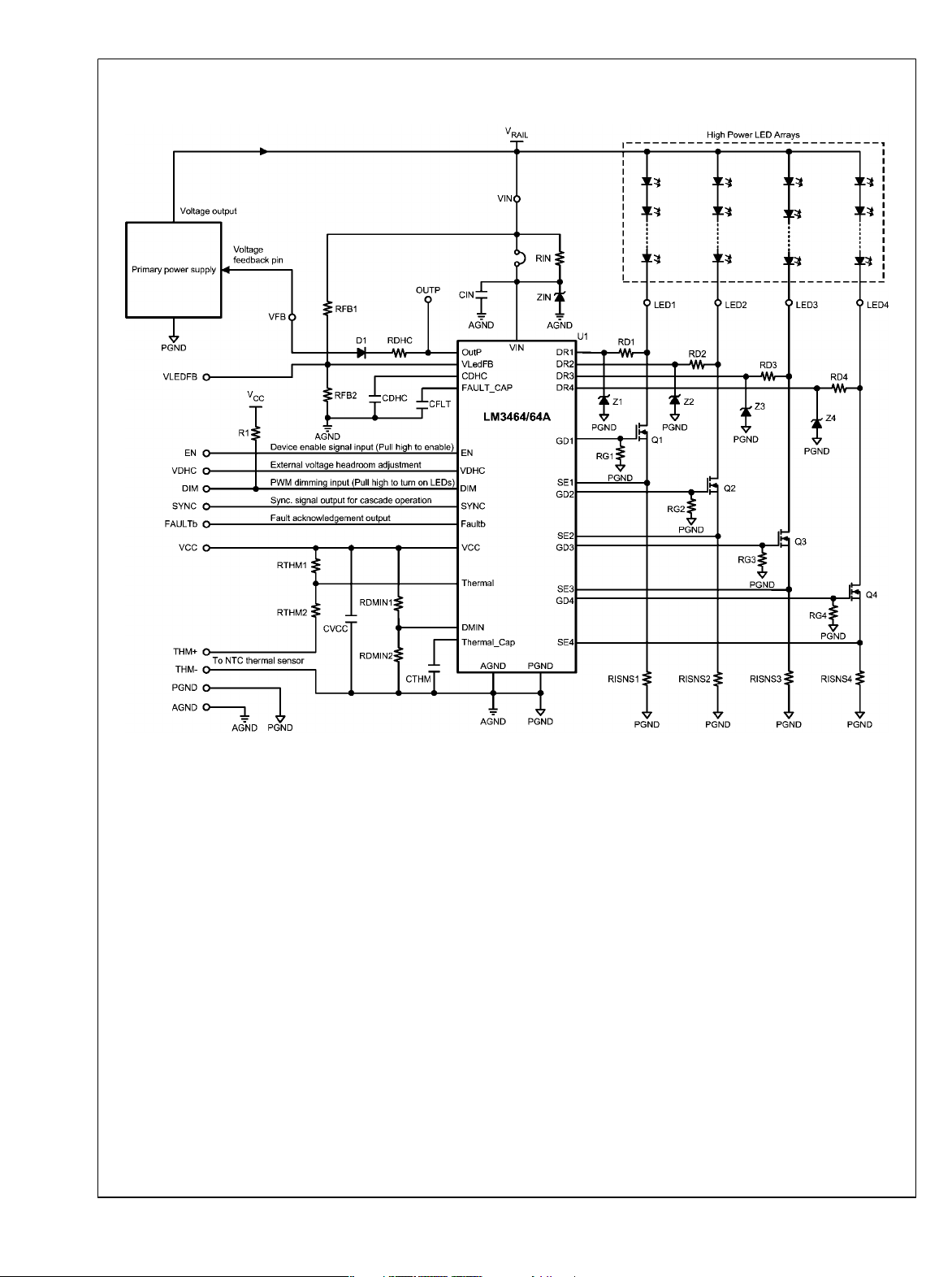
Evaluation Board Schematic
AN-2071
FIGURE 1. LM3464A Evaluation Board Schematic
www.national.com 2
30127101
Page 4

Bill of Materials
Designation Description Package Manufacturer Part # Vendor
U1 LED Driver IC, LM3464A eTSSOP-28 eTSSOP-28 LM3464AMH NSC
D1 Schottky Diode 40V 1.1A DO219AB DO219AB SL04-GS08 Vishay
Q1,Q2,Q3,Q4
CIN Cap MLCC 100V 2.2uF X7R 1210 1210 GRM32ER72A225KA35L Murata
CVCC Cap MLCC 10V 1uF X5R 0603 0603 GRM185R61A105KE36D Murata
CDHC Cap MLCC 50V 0.22uF X5R 0603 0603 GCM188R71H224KA64D Murata
CFLT Cap MLCC 50V 2.2nF X7R 0603 0603 GRM188R71H222KA01D Murata
CTHM Cap MLCC 50V 68nF X7R 0603 0603 GRM188R71H683KA01D Murata
R1 Chip Resistor 8.06Kohm 1% 0603 0603 CRCW06038K06FKEA Vishay
RTHM1 Chip Resistor 4.87Kohm 1% 0603 0603 CRCW06034K87FKEA Vishay
RTHM2 Chip Resistor 232ohm 1% 0603 0603 CRCW0603232RFKEA Vishay
RDMIN1 Chip Resistor 15.4Kohm 1% 0603 0603 CRCW060315K4FKEA Vishay
RDMIN2 Chip Resistor 1.05Kohm 1% 0603 0603 CRCW06031K05FKEA Vishay
RDHC Chip Resistor 2.67Kohm 1% 0603 0603 CRCW06032K67FKEA Vishay
RFB1 Chip Resistor 48.7Kohm 1% 0603 0603 CRCW060348K7FKEA Vishay
RFB2 Chip Resistor 2.67Kohm 1% 0603 0603 CRCW06032K67FKEA Vishay
RISNS1, RISNS2,
RISNS3, RISNS4
RIN, RD1, RD2, RD3,
RD4
VIN,PGND Banana Jack 5.3(mm) Dia 5.3 (mm) Dia. 575-8 Keystone
FAULTb,DIM, SYNC,
THM+, THM-,
AGND, VFB, VIN,
PGND, EN
LED1, LED2, LED3,
LED4
PCB LM3464EVAL PCB 82.5 X 60 (mm) 82.5 x 60 (mm) N/A NSC
RG1, R2, RG3, RG4 No Connection 0603
ZIN, Z1, Z2, Z3, Z4 No Connection SMA
MOSFET N-CH 150V 29A D-PAK D-PAK FDD2572 Fairchild
MOSFET N-CH 150V 50A TO252–3 TO252–3 IPD200N15N3 Infineon
Chip Resistor 1.13ohm 1% 0603 0603 CRCW06031R13FKEA Vishay
Chip Resistor 0ohm 1% 0603 0603 CRCW06030000Z0EA Vishay
Turret 2.35(mm) Dia 2.35 (mm) Dia. 1502-2 Keystone
Turret 2.35(mm) Dia 2.35 (mm) Dia. 1502-2 Keystone
Turret 2.35(mm) Dia 2.35 (mm) Dia. 1502-2 Keystone
AN-2071
3 www.national.com
Page 5
Connectors and Test Pins
AN-2071
30127102
FIGURE 2. Typical Connection Diagram
Evaluation Board Quick Setup Procedures
Terminal Designation Description
VIN Power supply positive (+ve) connection
PGND Power supply negative (-ve) connection
AGND LM3464A analog signal ground
LED1 Output Channel 1 (Connect to cathode of LED string 1)
LED2 Output Channel 2 (Connect to cathode of LED string 2)
LED3 Output Channel 3 (Connect to cathode of LED string 3)
LED4 Output Channel 4 (Connect to cathode of LED string 4)
EN LM3464A enable pin (pull down to disable)
VFB Connect to voltage feedback node of primary power supply for DHC
FAULTb Acknowledgement signal for arising of ‘FAULT’
DIM PWM dimming signal input (TTL signal compatible)
SYNC Synchronization signal for cascade operation
THM+ Connect to NTC thermal sensor for thermal foldback control
THM- Connect to NTC thermal sensor for thermal foldback control
VLEDFB Connected to LM3464A VLedFB pin
OUTP Connected to LM3464A OutP pin
VCC LM3464A internal voltage regulator output
VDHC Connected to LM3464A VDHC pin
www.national.com 4
Page 6
AN-2071
Structure of the System
A LM3464A LED lighting system is basically consist of three
main parts, the LM3464A evaluation board, an AC/DC power
supply and an LED array containing four LED strings. In general, the LM3464A evaluation board can be regarded as four
independent current sources that the dropout voltages on the
current sources are being monitored by an internal circuit that
generates the DHC signal. The LM3464A evaluation board is
designed to drive 4 LED strings of 12 LEDs in series. With
350mA driving current for every LED string, the default total
output power of the LM3464A evaluation board is around
60W. In order to ensure proper operation, the AC/DC power
supply and LED array should be selected following the steps
presented in this document.
Selection of AC/DC Power Supply
The LM3464A evaluation board can be powered by an AC/
DC power supply through the banana-plug type connectors
on the board as shown in figure 2. Assuming the nominal forward voltage of one LED is 3.5V, the total forward voltage of
a LED string containing 12 LED is about 42V. In order to reserve extra voltage headroom to compensate the variations
of the LED forward voltages due to changes of operation temperature, the LED turn ON voltage of this evaluation board is
set to 48V. As this evaluation board is designed to deliver
350mA for each output channel, which is about 60W output
power at 48V rail voltage, the AC/DC power supply must be
able to supply no less than 60W continuous output power at
48V. Therefore, a 60W AC/DC power supply with 48V output
voltage is needed.
In order to facilitate Dynamic Headroom Control (DHC), the
output voltage of the AC/DC power supply is adjusted by the
LM3464A. The LM3464A adjusts the output voltage of the AC/
DC power supply by sinking current from the output voltage
feedback node of the AC/DC converter through a resistor
RDHC into the OutP pin according to the dropout voltage of
the linear current regulators. The OutP pin of the LM3464A is
a open drain pin that can only sink current from the voltage
feedback node of the AC/DC power supply, thus the
LM3464A evaluation board is only able to increase the output
voltage of the AC/DC power supply to acquire wider voltage
headroom.
Since the output voltage of the AC/DC converter will be increased by the LM3464A to allow dynamic head room control
(DHC), the nominal output voltage of the AC/DC power supply
must be reduced prior to connecting to the LM3464A evaluation board to reserve voltage headroom for DHC to take
place. This is achieved by modifying the resistance of the
output voltage sensing resistors of the AC/DC power supply.
To adapt the AC/DC power supply to the LM3464A evaluation
board, the nominal output voltage of the AC/DC power supply
is recommended to be reduced from 48V to 36V. Usually, the
nominal output voltage of the AC/DC power supply can be
reduced by changing the resistance of the resistor divider for
output voltage feedback. Figure 2 shows the voltage feedback circuit using LM431 which has been widely used in
typical AC/DC power supplies as an example.
To reduce the output voltage of the AC/DC power supply from
48V to 36V, the resistance of R2 is increased without changing
the value of R1. The output voltage and value of R2 are related
by the following equations:
(1)
For V
And V
REF(AC/DC)
RAIL(nom)
= 2.5V
= 36V:
(2)
In the above equations, V
of the AC/DC converter for output voltage feedback. V
is the objective rail voltage level being adjusted to. In this
(nom)
example, reducing of the rail voltage is achieved by increasing
REF(AC/DC)
is the reference voltage
RAIL
the value of R2. With the rail voltage is reduced to 36V, the
LED strings are unable to be driven at 350mA due to insufficient voltage headroom until the DHC loop functions. In order
to ensure the LED strings an regulated driving current at the
time that the LED stings being turned on, the LM3464A increases the output voltage of the AC/DC power supply
(V
) from 36V to 48V (V
RAIL
LED strings. The level of V
of the resistors, RFB1 and RFB2. Figure 3 shows the changes
of V
upon the AC/DC power supply is powered until the
RAIL
system enters steady state operation.
DHC_READY
DHC_READY
) prior to turning on the
is defined by the value
As the output voltage of the AC/DC power supply is depending on the current being sunk from the output voltage feedback node of the AC/DC power supply, the output voltage
could increase to exceed the rated output voltage of the AC/
DC power supply and damage the system if the resistance of
the RDHC is too low and the OutP pin of the LM3464A is accidentally shortened to GND (V
value of the RDHC must be selected appropriately following
the equations below. In the equations, V
imum voltage that V
to GND. R1 and R2 are the resistors of the output voltage
can reach if the OutP pin is shortened
RAIL
= 0V). To avoid this, the
OutP
RAIL(peak)
is the max-
feedback resistor divider of the AC/DC power supply. When
designing the values of the RDHC, it is essential to ensure
that the V
of the AC/DC power supply, otherwise the AC/DC power sup-
RAIL(peak)
does not exceed the rated output voltage
ply could be damaged.
(3)
where
(4)
5 www.national.com
Page 7

AN-2071
FIGURE 3. Changes of Rail Voltage Upon Power Up
Setting of V
When V
pin of the LM3464A equals 2.5V. As the voltage at the
RAIL
DHC_READY
reaches V
DHC_READY
, the voltage at the VLedFB
VLedFB pin reaches 2.5V, the LM3464A performs a test for
no long than 400uS to identify and exclude the idle (no LED
connected) or failed (shorten / open circuit of LED string) output channels from the DHC loop. When a LED string is open
circuit, the voltage drop on the current sensing resistors
(V
— V
SE1
maintains below 30mV longer than the fault detection time
) is below 30mV. If the voltage of the SEx pin
SE4
defined by CFLT, an 'open fault' is recognized. When a LED
string is short circuit, causing the drain voltage of an external
MOSFET 8.4V higher than the drain voltage of any other
channel and maintains longer than the fault detection time
defined by CFLT, an short fault is recognized. Either a short
or open fault will cause the Faultb pin to pull low. When a LED
string experiences an open or short circuit, the corresponding
output channel will be disabled and excluded from the DHC
loop to sustain normal operation of the remaining LED strings.
The LM3464A will maintain the failed channels in disable
state until the EN pin is pulled low or the entire system is repowered. When the test is completed, the LM3464A enables
the output channels and provides constant current to the LED
strings.
The level of V
RFB2 on the evaluation board and can be adjusted to any
DHC_READY
is defined by the values of RFB1 and
level below 80V / 95V (LM3464/LM3464A) as desired. By default, the V
no more than 20V higher than the forward voltages of any LED
DHC_READY
is set at 48V. The V
DHC_READY
must set
30127103
string connected to the system under possible temperatures,
otherwise a ‘short fault’ may arise and results in immediate
output channel latch-off to protect the MOSFETs from overheat. The V
(5):
DHC_READY
is can be adjusted following equation
(5)
Adjusting Voltage Headroom
The voltage headroom of the LM3464A evaluation board can
be altered by adjusting the voltage at the VDHC pin (V
in the range of 0.8V to 2V. For the applications with high rail
voltage ripple, the voltage headroom should be increased to
secure accurate output current regulation. By default, the VDHC pin is biased internally to 0.9V as shown in figure 4.
VDHC
)
www.national.com 6
Page 8

30127104
FIGURE 4. Adjusting the VDHC Pin Voltage
To adjust V
tor divider (RA and RB) can be added across the VDHC test
pad and VCC or AGND terminals on the board. The values of
of RA and RB should be below 100kΩ and 16kΩ respectively
to ensure the accuracy of the headroom voltage under steady
state. The V
where
on the evaluation board, an additional resis-
VDHC
is governed by the following equation:
VDHC
(6)
Connecting the LED Strings
The LM3464A evaluation board is designed to drive 4 common anode LEDs strings of 12 serial LEDs per string. The
board includes four turret connectors, LED1, LED2, LED3 and
LED4 for cathode connections of the LED strings. The anode
of the LED strings should connect to the positive power output
terminal of the AC/DC power supply. By default, the output
current for each output channel is set at 350mA. The output
currents of the LM3464A evaluation board can be programmed individually by changing the value of the resistors
RISNS1, RISNS2, RISNS3 and RISNS4 accordingly. The
LED driving current is governed by the following equation:
(8)
Adjusting Frequency Response of the LM3464A Circuit
The frequency response of the LM3464A evaluation board
can be adjusted by changing the value of the capacitor,
C
. Higher capacitance of C
DHC
response of the LM3464A driver stage. In order to ensure
stable system operation, it is recommended to set the dominant pole of the LM3464A one decade lower than the dominant pole of the AC/DC converter. The default value of the
C
on the evaluation board is 0.22uF. For applications with
DHC
slow response AC/DC power supply (e.g. converters with active PFC), the value of CDHC should be increased to make
the frequency response of the board slower than the response
of the AC/DC power supply. The cut-off frequency of the
LM3464A driver stage is governed by the following equation:
results in slower frequency
DHC
AN-2071
(7)
(9)
7 www.national.com
Page 9

Thermal Foldback Control
The LM3464A evaluation board features an interface that en-
AN-2071
ables thermal foldback control by connecting a NTC thermal
sensor to the THM+ and THM- terminals. With the NTC sensor attached to the chassis of the LEDs, the integrated thermal foldback control circuit reduces the average LED current
and effectively reduces the LED temperature to prevent thermal breakdown of the LEDs. The thermal foldback control
circuit reduces the LED currents by means of PWM dimming
which the dimming frequency is set by the capacitor, CTHM
following the equation shows below:
(10)
The default value of the CTHM on the LM3464A evaluation
board is 68nF, which set the thermal foldback dimming frequency at 258Hz.
Thermal foldback control is activated when the voltage at the
Thermal pin, V
in figure 5. Thermal foldback control begins when V
below 3.25V. The LED current will be reduced to zero as
V
falls below 0.4V. The average LED current varies ac-
Thermal
cording to the Thermal pin voltage following the equation:
is in between 3.25V and 0.4V as shown
Thermal
Thermal
is
(11)
FIGURE 5. Changes of Average LED Current with Thermal Foldback Control
When the voltage at the DMIN pin is below 0.4V, the minimum
on time for thermal foldback control is restricted by the value
of C
. As the voltage of the Thermal pin is set below 0.4V,
THM
the on time for all output channels equals the discharge time
of the C
following the equation:
THM
(12)
30127113
Thus the minimum dimming duty cycle for thermal foldback is
calculated approximately equal to 0.5%:
(13)
www.national.com 8
Page 10

Design Example
AN-2071
FIGURE 6. Attaching NTC Thermistor to the LEDs
A NTC thermistor is connected to the THM+ and THM- terminals of the LM3464A evaluation board as shown in figure
6 to activate the thermal foldback control function.
Assuming that thermal foldback control is required to begin at
70°C LED chassis temperature and reduce 55% average LED
current (45% dimming duty cycle) when the chassis temperature reaches 125°C. Using the NTC thermister NXFT15WB473FA1B from MURATA, which has 4.704kΩ resistance at
70°C (R
V
at 125°C (45% dimming duty cycle):
Thermal
) and 1.436kΩ at 125°C (R
NTC(70°C)
NTC(125°C)
).
(14)
(15)
(16)
In the above equation, V
pin and D
back control. When thermal foldback begins:
is the dimming duty cycle under thermal fold-
THMFB
is the voltage at the Thermal
Thermal
(17)
(18)
(19)
When the temperature goes up to 125°C
30127114
(20)
By combining the equations (17) and (18), the values of
RTHM1 and RTHM2 can be obtained:
(21)
The default values of RTHM1 and RTHM2 on the LM3464A
evaluation board are 4.87kΩ and 232Ω respectively.
Minimum Dimming Duty Cycle for Thermal Foldback Control
The minimum dimming duty cycle for thermal foldback control
(D
THMFB_MIN
pin of the LM3464A. The minimum dimming duty cycle limit
overrides the minimum dimming level defined by RTHM1,
RTHM2 and the NTC thermistor. This function is especially
useful for the applications that require to maintain certain
brightness level under high operation temperature. The level
) can be limited by setting the voltage at the DMIN
9 www.national.com
Page 11

of minimum duty cycle limit is governed by the following equation:
AN-2071
PWM Dimming
PWM dimming control can be realized by applying PWM dimming signal to the DIM terminal of the board directly. When
the DIM pin is pulled to logic high, all output channles are
enabled. When the DIM pin is pulled to logic low (GND), all
(22)
output channels are turned OFF. In cascade operation, the
DIM signal should only be applied to the MASTER unit. The
LM3464A on the MASTER unit propagates the PWM dimming
signal on its DIM pin to the slave units one by one through the
SYNC pin. PWM dimming control is allowed when thermal
foldback control is activated. When PWM dimming and thermal foldback controls are required simultaneously, the PWM
dimming frequency should be set at least ten times below the
thermal foldback dimming frequency. The thermal foldback
dimming signal reduces the LED currents according to the
voltage at the Thermal pin when the signal at the DIM pin is
being pulled ‘high’ as shown in figure 7.
30127115
FIGURE 7. Thermal Foldback + PWM Dimming Control
www.national.com 10
Page 12

Cascade Operation
AN-2071
FIGURE 8. Cascading LM3464A Evaluation Boards for Output Channel Expansion
11 www.national.com
30127162
Page 13

The total output power of the LED lighting system can be expanded by cascading the LM3464A evaluation boards. In
cascade operation, the system involves one master unit and
AN-2071
multiple slave units. Both master and slave units are
LM3464A evaluation boards with minor modifications to program the LM3464A into master or slave modes. The connection diagram for cascade operation is shown in figure 8. The
master unit is responsible to provide functions as listed in below:
1. Detect rail voltage upon system startup
2. Command slave units to turn on LEDs as its VLedFB voltage reaches 2.5V
3. Provide dimming signal to slave units according to the
PWM dimming signal received at its DIM pin
4. Provide dimming signal to slave units according to the voltage of its Thermal pin
By default, the LM3464A evaluation board is set to master
mode. To set the board to slave mode, the following changes
to the board are required:
• Remove resistors RFB1 and RFB2
• Connect VLEDFB to VCC
When connecting the master and slaves, the following connections are required:
• Connect the VIN terminal of master and slave units together
and then to the POSITIVE output of the AC/DC power supply
• Connect the PGND terminal of master and slave units together and then to the NEGATIVE output of the AC/DC power
supply
• Connect the SYNC terminal of the master unit to DIM terminal of the next slave unit in the chain.
• Connect the VFB terminal of master and slave units together
and then to the voltage feedback node of the AC/DC power
supply.
If more than one slave unit is required, the SYNC pin of the
first slave unit should connect to the DIM pin of the next slave
unit to allow propagation of the control signal along the system
chain.
Connection To Led Arrays
When LEDs are connected to the LM3464A driver stage
through long cables, the parasitic components of the cable
harness and external MOSFETs may resonant and eventually lead to unstable system operation. In applications that the
cables between the LM3464A driver circuit and LED light engine are longer than 1 meter, a 4.7kΩ resistor should be
added across the GDx pins to GND as shown in Figure 12.
30127164
FIGURE 9. Additional Resistor Across GDx and SEx for
Cable Harness Over 1m Long
www.national.com 12
Page 14

AN-2071
FIGURE 10. Additional Voltage Clamping Circuits for V
Applications With High Rail Voltage
Since the LM3464A is rated to 95V supply voltage, applying
a voltage to any pin of the device exceeding the absolute rated
voltage could damage the device permanently. For the applications that the rail voltage could increase to exceed 95V,
external voltage clamping circuit must be added to the Vin and
DRx pins to avoid system breakdown. Figure 13 shows a typical application circuit with 150V peak rail voltage.
In figure 13, Z1, Z2, Z3, Z4 and ZIN are zener diodes for limiting
voltages at the DRx and VIN pins of the LM3464A. The reverse voltage of the selected zener diodes must not exceed
the rated voltage of the corresponding pin. For the LM3464A
30127165
RAIL(peak)
> 80V/95V (LM3464A)
evaluation board, the reverse voltage of the additional zener
diodes must not exceed 95V. The resistors R
R
, R
DR3
difference across the DRx pins and V
Calculating the Values of Zx and R
and RIN are resistors for absorbing the voltage
DR4
RAIL
DRx
.
:
DR1
, R
DR2
,
Since the current being passed through the zener diodes are
derived by the resistance of R
be calculated properly according to the reverse current of the
, the value of the R
DRx
DRx
must
zener diode and input current of the DRx pins of the LM3464A
avoid unnecessary power dissipations. For instant, a 500mW/
75V zener diode CMHZ5267B (Central Semiconductor) is
used to clamp the DRx pins at 75V. Because the reverse cur-
13 www.national.com
Page 15

rent of the CMHZ5267B is 1.7mA at 75V zener voltage, the
maximum allowable reverse current is 6.67mA at 500mW
power dissipation.
AN-2071
Given that the input current of the DRx pins of the LM3464A
at 100V is 63uA maximum, if the DRx pin voltage is below
100V, the current flowing into the DRx pin (I
63uA. In the following calculations, I
to reserve operation margin to compensate the characteris-
is assumed to 63uA
DRx
tics variations of the components.
Because V
pins, the maximum resistance of R
RAIL(peak)
lowing this equation:
is the possible highest voltage at the DRx
can be calculated fol-
DRx
Where VZ and IZ are the reverse voltage and current of the
zener diode Zx respectively.
For V
RAIL(peak)
= 150V, the maximum value of R
) is below
DRx
is:
DRx
Thus, a standard 42.2kΩ resistor with 0.25W power rating
(1206 package) and 1% tolerance can be used.
Calculating the Values of ZIN and RIN:
Assume the VIN pin of the LM3464A is about to be clamped
to 75V, a 1.5W/75V zener diode CMZ5946B from Central
Semiconductor is used to ensure adequate conduction current for ZIN. Because the reverse current of the CMZ5946B is
5mA at 75V, the allowable current flows through ZIN is in between 5mA to 20mA. Similar to the requirements of selecting
the Zx and R
is clamped to 75V by a voltage clamping circuit consists of
, the voltage at the VIN pin of the LM3464A
DRx
ZIN and RIN. Also since the maximum operating and shutdown current (VEN < 2.1V) are 3mA and 700uA respectively,
to ensure the voltage of the VIN pin is clamped close to 75V
even when the LM3464A is disabled, the value of RIN should
be calculated following the equations below:
Maximum value of RIN:
And the minimum value of R
Thus, the value of R
DRx
is:
DRx
must be selected in the range:
To minimize power dissipation on the zener diodes, a standard 42.2kΩ resistor can be used for the R
power dissipation on the R
is then equals to:
DRx
. The maximum
DRx
Minimum value of RIN:
So the value of RIN must be in the range:
To minimize power dissipations on both the ZIN and RIN, a
standard 9.31kΩ resistor can be selected for the RIN. Then
the maximum power dissipation on RIN is:
Thus, a standard 9.38kΩ resistor with 2512 package (1W)
and 1% tolerance can be used.
www.national.com 14
Page 16

AN-2071
Typical Performance and Waveforms All curves taken at V
= 48V with configuration in typical
IN
application for driving twelve power LEDs with four output channels active and output current per channel = 350mA. TA = 25°C,
unless otherwise specified.
Output Current Variation
30127120
VCC Variation (%)
Efficiency (%)
30127121
DHC in Cascade Operation
V
of Master Unit
SYNC
30127122
30127124
30127123
V
at System Startup
SYNC
30127125
15 www.national.com
Page 17

Evaluation Board Layout
AN-2071
30127126
FIGURE 11. Top Layer and Top Overlay
30127127
FIGURE 12. Bottom Layer and Bottom Overlay
www.national.com 16
Page 18

Notes
AN-2071
17 www.national.com
Page 19

Notes
For more National Semiconductor product information and proven design tools, visit the following Web sites at:
www.national.com
Products Design Support
Amplifiers www.national.com/amplifiers WEBENCH® Tools www.national.com/webench
Audio www.national.com/audio App Notes www.national.com/appnotes
Clock and Timing www.national.com/timing Reference Designs www.national.com/refdesigns
Data Converters www.national.com/adc Samples www.national.com/samples
Interface www.national.com/interface Eval Boards www.national.com/evalboards
LVDS www.national.com/lvds Packaging www.national.com/packaging
Power Management www.national.com/power Green Compliance www.national.com/quality/green
Switching Regulators www.national.com/switchers Distributors www.national.com/contacts
LDOs www.national.com/ldo Quality and Reliability www.national.com/quality
LED Lighting www.national.com/led Feedback/Support www.national.com/feedback
Voltage References www.national.com/vref Design Made Easy www.national.com/easy
PowerWise® Solutions www.national.com/powerwise Applications & Markets www.national.com/solutions
Serial Digital Interface (SDI) www.national.com/sdi Mil/Aero www.national.com/milaero
Temperature Sensors www.national.com/tempsensors SolarMagic™ www.national.com/solarmagic
PLL/VCO www.national.com/wireless PowerWise® Design
University
www.national.com/training
THE CONTENTS OF THIS DOCUMENT ARE PROVIDED IN CONNECTION WITH NATIONAL SEMICONDUCTOR CORPORATION
(“NATIONAL”) PRODUCTS. NATIONAL MAKES NO REPRESENTATIONS OR WARRANTIES WITH RESPECT TO THE ACCURACY
OR COMPLETENESS OF THE CONTENTS OF THIS PUBLICATION AND RESERVES THE RIGHT TO MAKE CHANGES TO
SPECIFICATIONS AND PRODUCT DESCRIPTIONS AT ANY TIME WITHOUT NOTICE. NO LICENSE, WHETHER EXPRESS,
IMPLIED, ARISING BY ESTOPPEL OR OTHERWISE, TO ANY INTELLECTUAL PROPERTY RIGHTS IS GRANTED BY THIS
DOCUMENT.
TESTING AND OTHER QUALITY CONTROLS ARE USED TO THE EXTENT NATIONAL DEEMS NECESSARY TO SUPPORT
NATIONAL’S PRODUCT WARRANTY. EXCEPT WHERE MANDATED BY GOVERNMENT REQUIREMENTS, TESTING OF ALL
PARAMETERS OF EACH PRODUCT IS NOT NECESSARILY PERFORMED. NATIONAL ASSUMES NO LIABILITY FOR
APPLICATIONS ASSISTANCE OR BUYER PRODUCT DESIGN. BUYERS ARE RESPONSIBLE FOR THEIR PRODUCTS AND
APPLICATIONS USING NATIONAL COMPONENTS. PRIOR TO USING OR DISTRIBUTING ANY PRODUCTS THAT INCLUDE
NATIONAL COMPONENTS, BUYERS SHOULD PROVIDE ADEQUATE DESIGN, TESTING AND OPERATING SAFEGUARDS.
EXCEPT AS PROVIDED IN NATIONAL’S TERMS AND CONDITIONS OF SALE FOR SUCH PRODUCTS, NATIONAL ASSUMES NO
LIABILITY WHATSOEVER, AND NATIONAL DISCLAIMS ANY EXPRESS OR IMPLIED WARRANTY RELATING TO THE SALE
AND/OR USE OF NATIONAL PRODUCTS INCLUDING LIABILITY OR WARRANTIES RELATING TO FITNESS FOR A PARTICULAR
PURPOSE, MERCHANTABILITY, OR INFRINGEMENT OF ANY PATENT, COPYRIGHT OR OTHER INTELLECTUAL PROPERTY
RIGHT.
LIFE SUPPORT POLICY
NATIONAL’S PRODUCTS ARE NOT AUTHORIZED FOR USE AS CRITICAL COMPONENTS IN LIFE SUPPORT DEVICES OR
SYSTEMS WITHOUT THE EXPRESS PRIOR WRITTEN APPROVAL OF THE CHIEF EXECUTIVE OFFICER AND GENERAL
COUNSEL OF NATIONAL SEMICONDUCTOR CORPORATION. As used herein:
Life support devices or systems are devices which (a) are intended for surgical implant into the body, or (b) support or sustain life and
whose failure to perform when properly used in accordance with instructions for use provided in the labeling can be reasonably expected
to result in a significant injury to the user. A critical component is any component in a life support device or system whose failure to perform
can be reasonably expected to cause the failure of the life support device or system or to affect its safety or effectiveness.
National Semiconductor and the National Semiconductor logo are registered trademarks of National Semiconductor Corporation. All other
brand or product names may be trademarks or registered trademarks of their respective holders.
Copyright© 2011 National Semiconductor Corporation
For the most current product information visit us at www.national.com
National Semiconductor
Americas Technical
Support Center
Email: support@nsc.com
AN-2071 LM3464A 4 Channel LED Driver Evaluation Board
www.national.com
Tel: 1-800-272-9959
National Semiconductor Europe
Technical Support Center
Email: europe.support@nsc.com
National Semiconductor Asia
Pacific Technical Support Center
Email: ap.support@nsc.com
National Semiconductor Japan
Technical Support Center
Email: jpn.feedback@nsc.com
Page 20

IMPORTANT NOTICE
Texas Instruments Incorporated and its subsidiaries (TI) reserve the right to make corrections, modifications, enhancements, improvements,
and other changes to its products and services at any time and to discontinue any product or service without notice. Customers should
obtain the latest relevant information before placing orders and should verify that such information is current and complete. All products are
sold subject to TI’s terms and conditions of sale supplied at the time of order acknowledgment.
TI warrants performance of its hardware products to the specifications applicable at the time of sale in accordance with TI’s standard
warranty. Testing and other quality control techniques are used to the extent TI deems necessary to support this warranty. Except where
mandated by government requirements, testing of all parameters of each product is not necessarily performed.
TI assumes no liability for applications assistance or customer product design. Customers are responsible for their products and
applications using TI components. To minimize the risks associated with customer products and applications, customers should provide
adequate design and operating safeguards.
TI does not warrant or represent that any license, either express or implied, is granted under any TI patent right, copyright, mask work right,
or other TI intellectual property right relating to any combination, machine, or process in which TI products or services are used. Information
published by TI regarding third-party products or services does not constitute a license from TI to use such products or services or a
warranty or endorsement thereof. Use of such information may require a license from a third party under the patents or other intellectual
property of the third party, or a license from TI under the patents or other intellectual property of TI.
Reproduction of TI information in TI data books or data sheets is permissible only if reproduction is without alteration and is accompanied
by all associated warranties, conditions, limitations, and notices. Reproduction of this information with alteration is an unfair and deceptive
business practice. TI is not responsible or liable for such altered documentation. Information of third parties may be subject to additional
restrictions.
Resale of TI products or services with statements different from or beyond the parameters stated by TI for that product or service voids all
express and any implied warranties for the associated TI product or service and is an unfair and deceptive business practice. TI is not
responsible or liable for any such statements.
TI products are not authorized for use in safety-critical applications (such as life support) where a failure of the TI product would reasonably
be expected to cause severe personal injury or death, unless officers of the parties have executed an agreement specifically governing
such use. Buyers represent that they have all necessary expertise in the safety and regulatory ramifications of their applications, and
acknowledge and agree that they are solely responsible for all legal, regulatory and safety-related requirements concerning their products
and any use of TI products in such safety-critical applications, notwithstanding any applications-related information or support that may be
provided by TI. Further, Buyers must fully indemnify TI and its representatives against any damages arising out of the use of TI products in
such safety-critical applications.
TI products are neither designed nor intended for use in military/aerospace applications or environments unless the TI products are
specifically designated by TI as military-grade or "enhanced plastic." Only products designated by TI as military-grade meet military
specifications. Buyers acknowledge and agree that any such use of TI products which TI has not designated as military-grade is solely at
the Buyer's risk, and that they are solely responsible for compliance with all legal and regulatory requirements in connection with such use.
TI products are neither designed nor intended for use in automotive applications or environments unless the specific TI products are
designated by TI as compliant with ISO/TS 16949 requirements. Buyers acknowledge and agree that, if they use any non-designated
products in automotive applications, TI will not be responsible for any failure to meet such requirements.
Following are URLs where you can obtain information on other Texas Instruments products and application solutions:
Products Applications
Audio www.ti.com/audio Communications and Telecom www.ti.com/communications
Amplifiers amplifier.ti.com Computers and Peripherals www.ti.com/computers
Data Converters dataconverter.ti.com Consumer Electronics www.ti.com/consumer-apps
DLP® Products www.dlp.com Energy and Lighting www.ti.com/energy
DSP dsp.ti.com Industrial www.ti.com/industrial
Clocks and Timers www.ti.com/clocks Medical www.ti.com/medical
Interface interface.ti.com Security www.ti.com/security
Logic logic.ti.com Space, Avionics and Defense www.ti.com/space-avionics-defense
Power Mgmt power.ti.com Transportation and Automotive www.ti.com/automotive
Microcontrollers microcontroller.ti.com Video and Imaging www.ti.com/video
RFID www.ti-rfid.com
OMAP Mobile Processors www.ti.com/omap
Wireless Connectivity www.ti.com/wirelessconnectivity
TI E2E Community Home Page e2e.ti.com
Mailing Address: Texas Instruments, Post Office Box 655303, Dallas, Texas 75265
Copyright © 2011, Texas Instruments Incorporated
 Loading...