

Page 1
I
COLL
V+
BR1
VAC
TRIAC
DIMMER
+
+
1
2
3
4
5 6
7
8
9
10
-
V
LED
GND
VCC
FLTR2
ASNS
FLTR1
ISNS
GATE
BLDR
COFF
DIM
LM3445MM
V
LED-
D3
C7
C9
C10
D4
D8
D9
R2
D1
Q1
C5
R5
C12
D2
D10
Q2
L2
Q3
R3
R4
C11
C4
C3
R1
U1
V
BUCK
LINE VOLTAGE (VAC)
EFFICIENCY (%)
95.0
90.0
85.0
80.0
75.0
80 90 100 110 120 130 140
14 Series connected LEDs
10 Series connected LEDs
LM3445
www.ti.com
SNVS570L –JANUARY 2009–REVISED MAY 2013
Triac Dimmable Offline LED Driver
Check for Samples: LM3445
1
FEATURES
2
• Triac Dim Decoder Circuit for LED Dimming
• Application Voltage Range 80VAC– 277V
AC
• Capable of Controlling LED Currents Greater
Than 1A
• Adjustable Switching Frequency
• Low Quiescent Current
• Adaptive Programmable Off-Time Allows for
Constant Ripple Current
• Thermal Shutdown
• No 120Hz Flicker
• Low Profile 10-Pin VSSOP Package or 14-Pin
SOIC voltage to the buck regulator. Additional features
• Patent Pending Drive Architecture
APPLICATIONS
• Retro Fit Triac Dimming
• Solid State Lighting
• Industrial and Commercial Lighting
• Residential Lighting
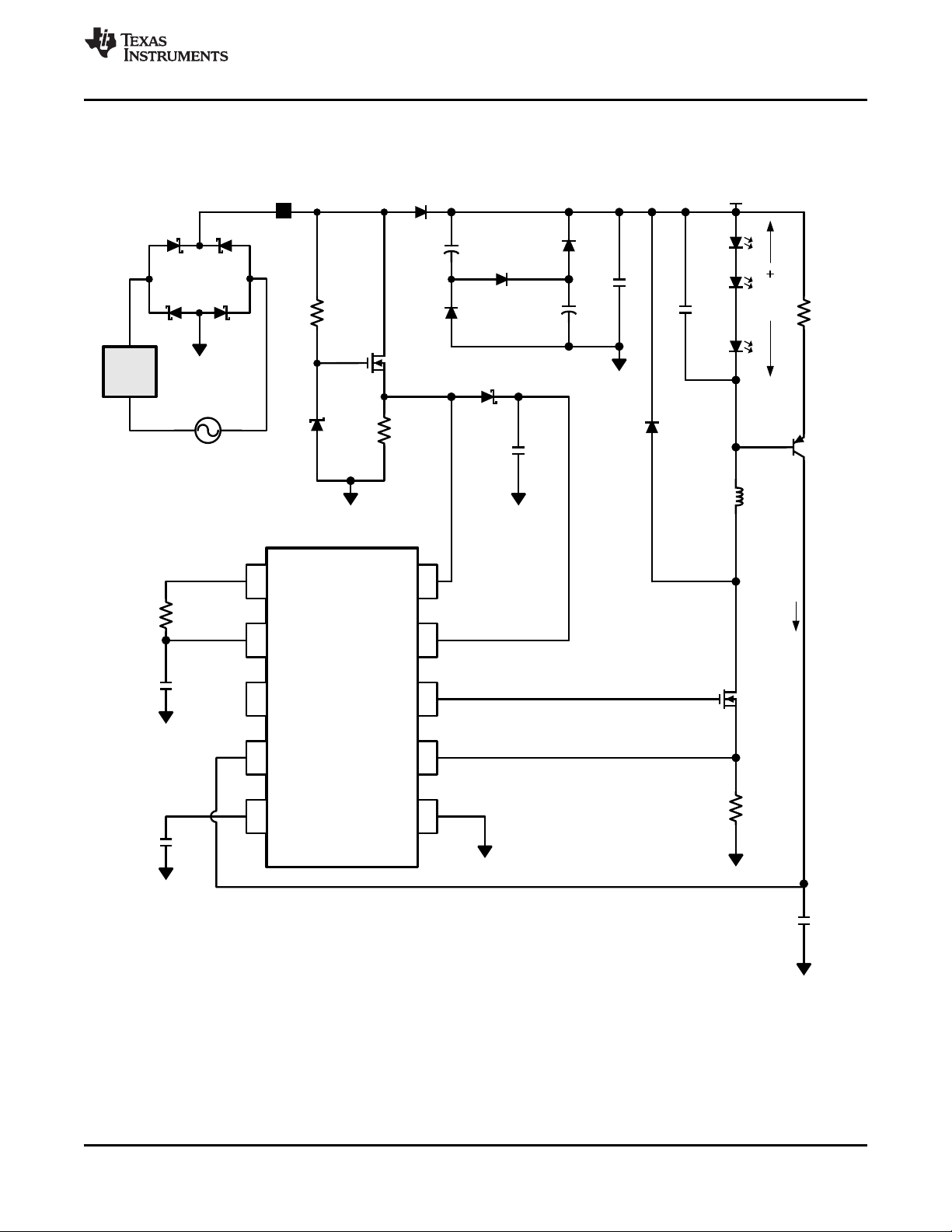
DESCRIPTION
The LM3445 is an adaptive constant off-time AC/DC
buck (step-down) constant current controller designed
to be compatible with triac dimmers. The LM3445
provides a constant current for illuminating high
power LEDs and includes a triac dim decoder. The
dim decoder allows wide range LED dimming using
standard triac dimmers. The high frequency capable
architecture allows the use of small external passive
components. The LM3445 includes a bleeder circuit
to ensure proper triac operation by allowing current
flow while the line voltage is low to enable proper
firing of the triac. A passive PFC circuit ensures good
power factor by drawing current directly from the line
for most of the cycle, and provides a constant positive
include thermal shutdown, current limit and V
under-voltage lockout.
CC
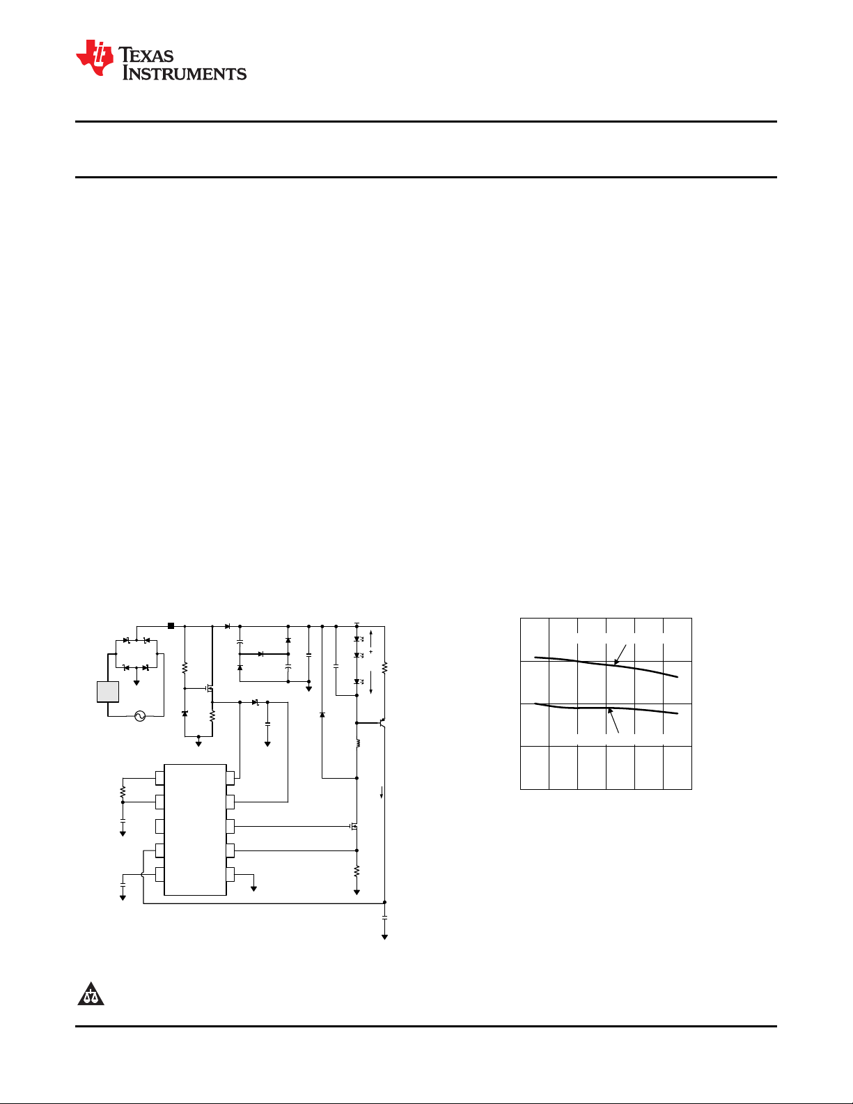
Typical LM3445 LED Driver Application Circuit
1
2All trademarks are the property of their respective owners.
PRODUCTION DATA information is current as of publication date.
Products conform to specifications per the terms of the Texas
Instruments standard warranty. Production processing does not
necessarily include testing of all parameters.
Please be aware that an important notice concerning availability, standard warranty, and use in critical applications of
Texas Instruments semiconductor products and disclaimers thereto appears at the end of this data sheet.
Copyright © 2009–2013, Texas Instruments Incorporated
Page 2
1
4
3
2
14
11
12
13
N/C
N/C
ASNS
DIM
GND
FLTR1
COFF
FLTR2
5 10N/C BLDR
6N/C
7ISNS
9
VCC
8 GATE
1
4
3
2
10
7
8
9
I
SNS
FLTR1
GATE
BLDR
COFF
V
CC
ASNS
DIM
5 6FLTR2 GND
LM3445
SNVS570L –JANUARY 2009–REVISED MAY 2013
www.ti.com
DEVICE INFORMATION
ORDER NUMBER
LM3445M/NOPB SULB
LM3445MM/NOPB SULB
LM3445MMX/NOPB LM3445M
LM3445MX/NOPB LM3445M
(1) For the most current package and ordering information, see the Package Option Addendum at the end of this document, or see the TI
web site at www.ti.com.
(1)
TOP MARK
Connection Diagram
Top View Top View
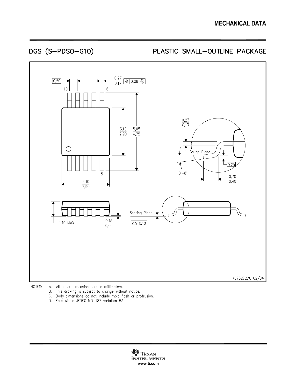
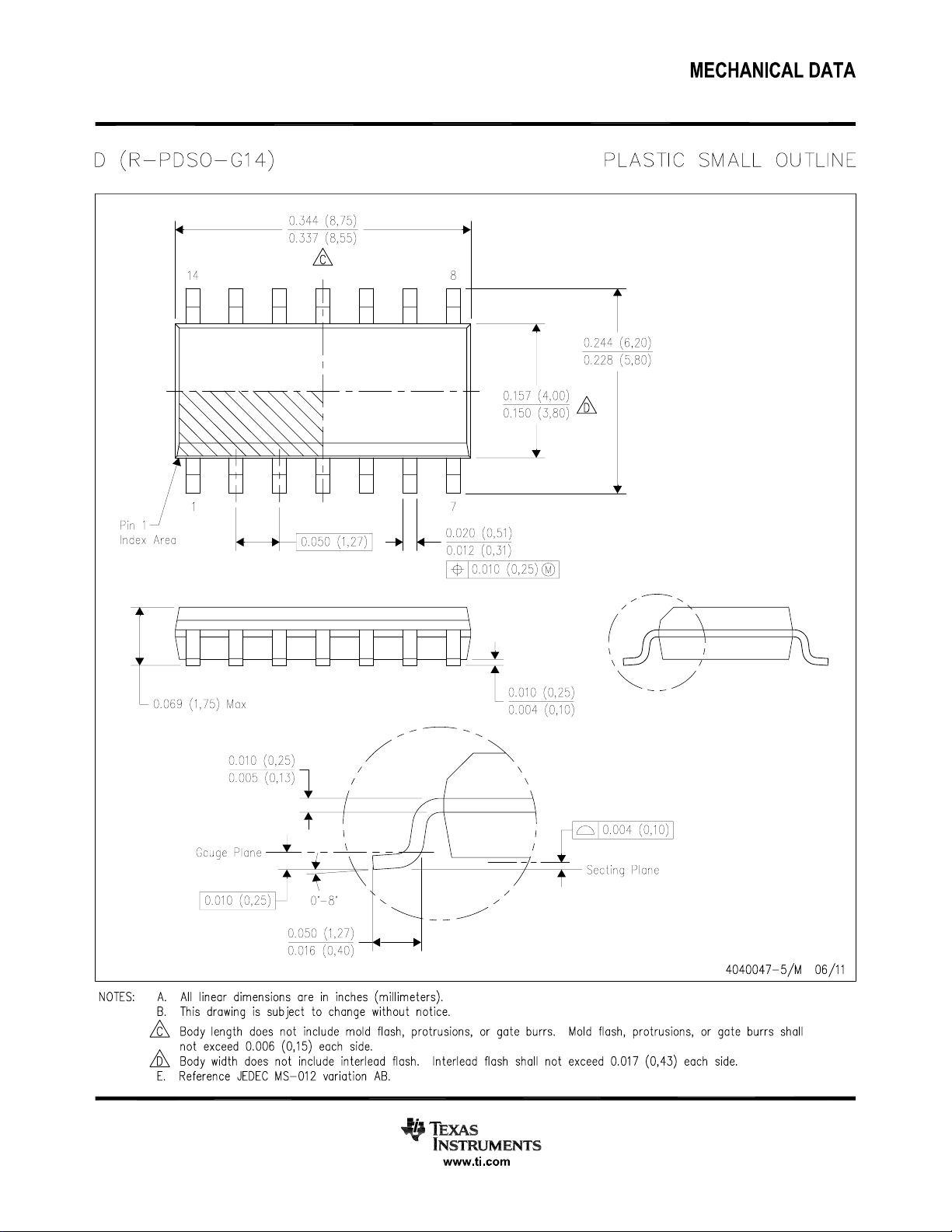
Figure 1. 10-Pin VSSOP Figure 2. 14-Pin SOIC
Package Number DGS Package Number D
SOIC VSSOP Name Description
12 1 ASNS PWM output of the triac dim decoder circuit. Outputs a 0 to 4V PWM signal with a duty cycle
13 2 FLTR1 First filter input. The 120Hz PWM signal from ASNS is filtered to a DC signal and compared to a 1 to
14 3 DIM Input/output dual function dim pin. This pin can be driven with an external PWM signal to dim the
1 4 COFF OFF time setting pin. A user set current and capacitor connected from the output to this pin sets the
3 5 FLTR2 Second filter input. A capacitor tied to this pin filters the PWM dimming signal to supply a DC voltage
4 6 GND Circuit ground connection.
7 7 ISNS LED current sense pin. Connect a resistor from main switching MOSFET source, ISNS to GND to set
8 8 GATE Power MOSFET driver pin. This output provides the gate drive for the power switching MOSFET of the
9 9 V
10 10 BLDR Bleeder pin. Provides the input signal to the angle detect circuitry as well as a current path through a
2,5,6,11 - N/C No Connect
CC
PIN DESCRIPTIONS
proportional to the triac dimmer on-time.
3V, 5.85 kHz ramp to generate a higher frequency PWM signal with a duty cycle proportional to the
triac dimmer firing angle. Pull above 4.9V (typical) to tri-state DIM.
LEDs. It may also be used as an output signal and connected to the DIM pin of other LM3445s or
other LED drivers to dim multiple LED circuits simultaneously.
constant OFF time of the switching controller.
to control the LED current. Could also be used as an analog dimming input.
the maximum LED current.
buck controller.
Input voltage pin. This pin provides the power for the internal control circuitry and gate driver.
switched 230Ω resistor to ensure proper firing of the triac dimmer.
2 Submit Documentation Feedback Copyright © 2009–2013, Texas Instruments Incorporated
Product Folder Links: LM3445
Page 3
LM3445
www.ti.com
SNVS570L –JANUARY 2009–REVISED MAY 2013
These devices have limited built-in ESD protection. The leads should be shorted together or the device placed in conductive foam
during storage or handling to prevent electrostatic damage to the MOS gates.
ABSOLUTE MAXIMUM RATINGS
(1)(2)
BLDR to GND -0.3V to +17V
VCC, GATE, FLTR1 to GND -0.3V to +14V
ISNS to GND -0.3V to +2.5V
ASNS, DIM, FLTR2, COFF to GND -0.3V to +7.0V
COFF Input Current 100mA
Continuous Power Dissipation
ESD Susceptibility, HBM
Junction Temperature (T
(3)
(4)
) 150°C
J-MAX
Internally Limited
2 kV
Storage Temperature Range -65°C to +150°C
Maximum Lead Temperature Range (Soldering) 260°C
(1) Absolute maximum ratings are limits beyond which damage to the device may occur. Operating Ratings are conditions for which the
device is intended to be functional, but device parameter specifications may not be guaranteed. For ensured specifications and test
conditions, see the Electrical Characteristics. All voltages are with respect to the potential at the GND pin, unless otherwise specified.
(2) If Military/Aerospace specified devices are required, please contact the Texas Instruments Sales Office/Distributors for availability and
specifications.
(3) Internal thermal shutdown circuitry protects the device from permanent damage. Thermal shutdown engages at TJ= 165°C (typ.) and
disengages at TJ= 145°C (typ).
(4) Human Body Model, applicable std. JESD22-A114-C.
OPERATING CONDITIONS
V
CC
Junction Temperature −40°C to +125°C
8.0V to 12V
ELECTRICAL CHARACTERISTICS
Limits in standard type face are for TJ= 25°C and those with boldface type apply over the full Operating Temperature
Range ( TJ= −40°C to +125°C). Minimum and Maximum limits are specified through test, design, or statistical correlation.
Typical values represent the most likely parametric norm at TJ= +25ºC, and are provided for reference purposes only.
Symbol Parameter Conditions Min Typ Max Units
BLEEDER
R
BLDR
VCCSUPPLY
I
VCC
V
CC-UVLO
COFF
V
COFF
R
COFF
t
COFF
CURRENT LIMIT
V
ISNS
t
ISNS
Bleeder resistance to GND I
= 10mA 230 325 Ω
BLDR
Operating supply current 2.00 2.85 mA
Rising threshold 7.4 7.7 V
Falling threshold 6.0 6.4
Hysterisis 1
Time out threshold 1.225 1.276 1.327 V
Off timer sinking impedance 33 60 Ω
Restart timer 180 µs
ISNS limit threshold 1.174 1.269 1.364 V
Leading edge blanking time 125 ns
Current limit reset delay 180 µs
ISNS limit to GATE delay ISNS = 0 to 1.75V step 33 ns
Copyright © 2009–2013, Texas Instruments Incorporated Submit Documentation Feedback 3
Product Folder Links: LM3445
Page 4
LM3445
SNVS570L –JANUARY 2009–REVISED MAY 2013
www.ti.com
ELECTRICAL CHARACTERISTICS (continued)
Limits in standard type face are for TJ= 25°C and those with boldface type apply over the full Operating Temperature
Range ( TJ= −40°C to +125°C). Minimum and Maximum limits are specified through test, design, or statistical correlation.
Typical values represent the most likely parametric norm at TJ= +25ºC, and are provided for reference purposes only.
Symbol Parameter Conditions Min Typ Max Units
INTERNAL PWM RAMP
f
RAMP
V
RAMP
D
RAMP
DIM DECODER
t
ANG_DET
V
ASNS
I
ASNS
V
DIM
V
TSTH
R
DIM
CURRENT SENSE COMPARATOR
V
FLTR2
R
FLTR2
V
OS
GATE DRIVE OUTPUT
V
DRVH
V
DRVL
I
DRV
t
DV
THERMAL SHUTDOWN
T
SD
THERMAL SHUTDOWN
R
θJA
Frequency 5.85 kHz
Valley voltage 0.96 1.00 1.04 V
Peak voltage 2.85 3.00 3.08
Maximum duty cycle 96.5 98.0 %
Angle detect rising threshold Observed on BLDR pin 6.79 7.21 7.81 V
ASNS filter delay 4 µs
ASNS VMAX 3.85 4.00 4.15 V
ASNS drive capability sink V
ASNS drive capability source V
DIM low sink current V
DIM High source current V
= 2V 7.6 mA
ASNS
= 2V -4.3
ASNS
= 1V 1.65 2.80
DIM
= 4V -4.00 -3.00
DIM
DIM low voltage PWM input voltage 0.9 1.33 V
threshold
DIM high voltage 2.33 3.15
Tri-state threshold voltage Apply to FLTR1 pin 4.87 5.25 V
DIM comparator tri-state impedance 10 MΩ
FLTR2 open circuit voltage 720 750 780 mV
FLTR2 impedance 420 kΩ
Current sense comparator offset voltage -4.0 0.1 4.0 mV
GATE high saturation I
GATE low saturation I
= 50 mA 0.24 0.50 V
GATE
= 100 mA 0.22 0.50
GATE
Peak souce current GATE = VCC/2 -0.77 A
Peak sink current GATE = VCC/2 0.88
Rise time C
Fall time C
Thermal shutdown temperature See
= 1 nF 15 ns
load
= 1 nF 15
load
(1)
165 °C
Thermal shutdown hysteresis 20
VSSOP-10 junction to ambient 121 °C/W
(1) Junction-to-ambient thermal resistance is highly application and board-layout dependent. In applications where high maximum power
dissipation exists, special care must be paid to thermal dissipation issues in board design. In applications where high power dissipation
and/or poor package thermal resistance is present, the maximum ambient temperature may have to be derated. Maximum ambient
temperature (T
of the device in the application (P
given by the following equation: T
) is dependent on the maximum operating junction temperature (T
A-MAX
), and the junction-to ambient thermal resistance of the part/package in the application (R
D-MAX
A-MAX
= T
J-MAX-OP
– (R
θJA
× P
D-MAX
).
J-MAX-OP
= 125°C), the maximum power dissipation
), as
θJA
4 Submit Documentation Feedback Copyright © 2009–2013, Texas Instruments Incorporated
Product Folder Links: LM3445
Page 5
200.0
190.0
180.0
170.0
160.0
150.0
-50 -25 0 25 50 75 100 125 150
TEMPERATURE (°C)
t
ON-MIN
(ns)
V
OFF
(V)
1.29
1.28
1.27
1.26
1.25
-50 -25 0 25 50 75 100 125 150
OFF Threshold at C11
TEMPERATURE (°C)
UVLO
(V)
8.0
7.5
7.0
6.5
6.0
-50 -25 0 25 50 75 100 125 150
UVLO (VCC) Rising
UVLO (VCC) Falling
TEMPERATURE (°C)
BLDR RESISTOR (Ö)
300
280
260
240
220
200
-50 -25 0 25 50 75 100 125 150
TEMPERATURE (°C)
LINE VOLTAGE (VAC)
f
SW
(Hz)
300k
250k
200k
150k
100k
50k
0
80 90 100 110 120 130 140
C11 = 2.2 nF, R3 = 348 k:
7 LEDs in Series (V
O
= 24.5V)
LINE VOLTAGE (VAC)
EFFICIENCY (%)
95.0
90.0
85.0
80.0
75.0
80 90 100 110 120 130 140
14 Series connected LEDs
10 Series connected LEDs
LM3445
www.ti.com
SNVS570L –JANUARY 2009–REVISED MAY 2013
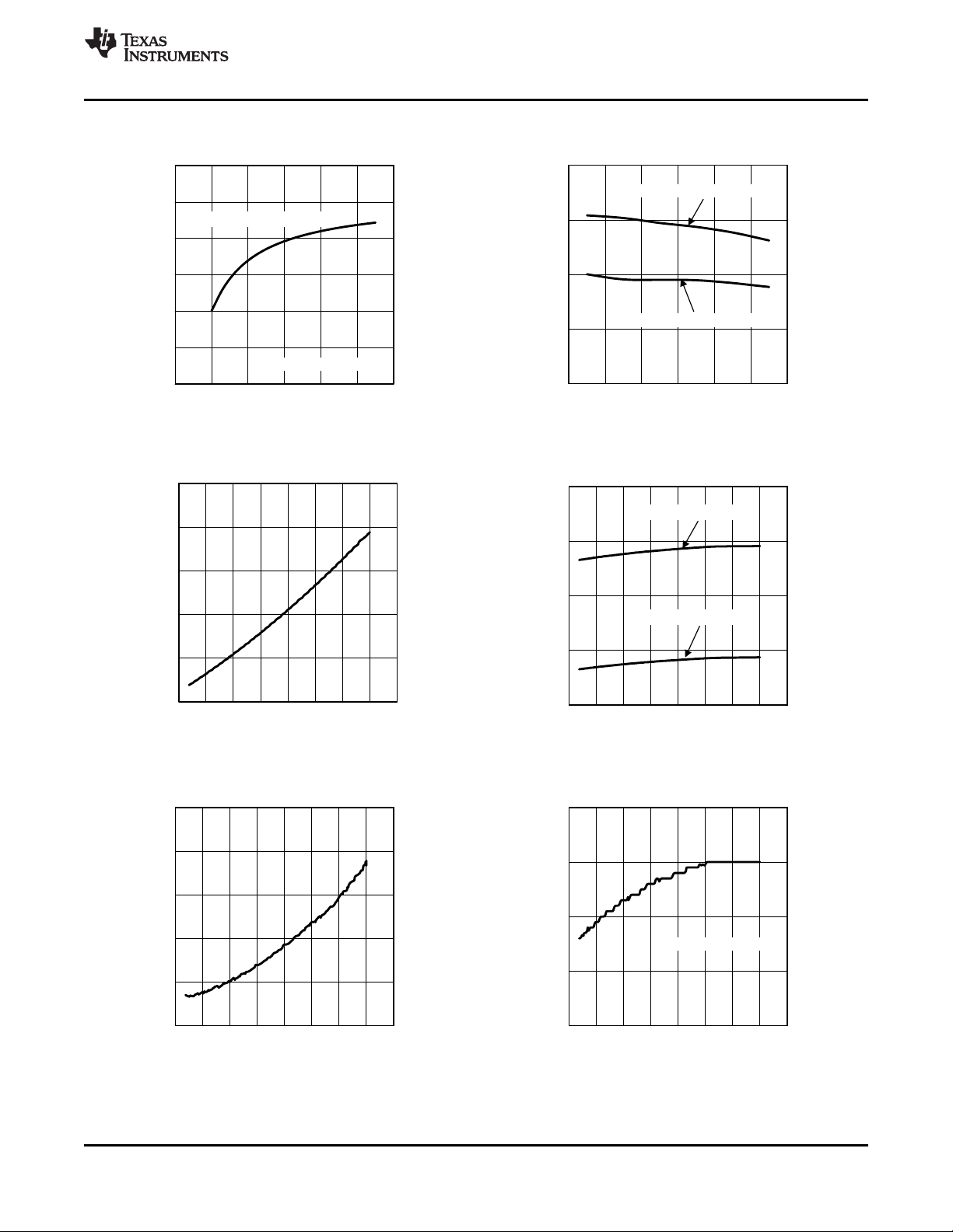
TYPICAL PERFORMANCE CHARACTERISTICS
fSWvs Input Line Voltage Efficiency vs Input Line Voltage
Figure 3. Figure 4.
BLDR Resistor vs Temperature VCCUVLO vs Temperature
Min On-Time (tON) vs Temperature Off Threshold (C11) vs Temperature
Copyright © 2009–2013, Texas Instruments Incorporated Submit Documentation Feedback 5
Figure 5. Figure 6.
Figure 7. Figure 8.
Product Folder Links: LM3445
Page 6
V
BUCK
(V)
NORMALIZED SW FREQ
1.50
1.25
1.00
0.75
0.50
0.25
0 50 100 150 200
3 LEDs
5 LEDs
7 LEDs
9 LEDs
Series
connected LEDs
LEADING EDGE BLANKING (ns)
NUMBER OF UNITS
15.0
10.0
5.0
0.0
80 100 120 140 160 180
Room (25°C)
Hot (125°C)
Cold (-40°C)
100 units tested
LM3445
SNVS570L –JANUARY 2009–REVISED MAY 2013
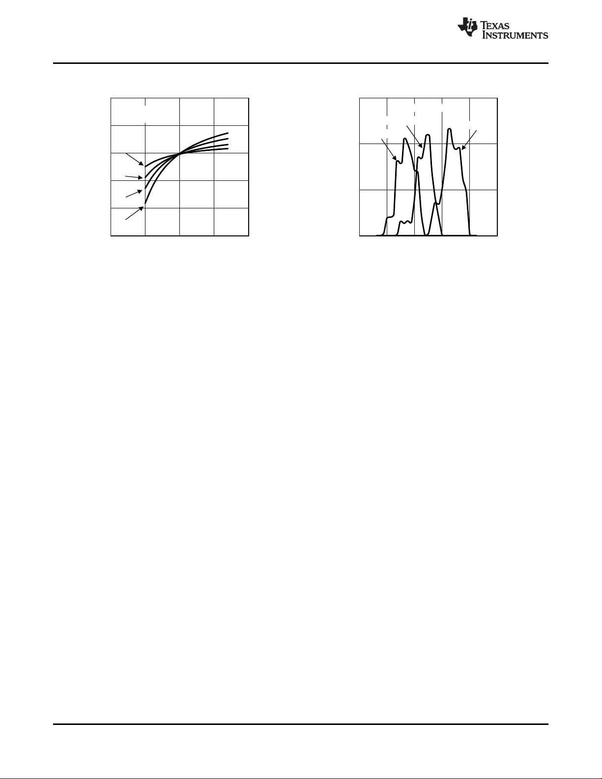
TYPICAL PERFORMANCE CHARACTERISTICS (continued)
Normalized Variation in fSWover V
Figure 9. Figure 10.
Voltage Leading Edge Blanking Variation Over Temperature
BUCK
www.ti.com
6 Submit Documentation Feedback Copyright © 2009–2013, Texas Instruments Incorporated
Product Folder Links: LM3445
Page 7
BRIGHT
DIM
MAINS AC
R1 250 kÖ
DIAC
LOAD
R2 3.3 kÖ
C1 100 nF
TRIAC
LM3445
7.2V
VCC UVLO
SRQ
PWM
I-LIM
1.27V
ISNS
ASNS
COFF
MOSFET
DRIVER
GND
FLTR1
FLTR2
DIM
VCC
ANGLE DETECT
BLEEDER
DIM DECODER
1.276V
4.9V
RAMP
0V to 4V
THERMAL
SHUTDOWN
50k
370k
1k
RAMP GEN.
5.9 kHz
3V
1V
INTERNAL
REGULATORS
750 mV
33:
125 ns
LEADING EDGE BLANKING
Tri-State
COFF
LATCH
CONTROLLER
START
4 Ps
BLDR
230
GATE
LM3445
www.ti.com
SNVS570L –JANUARY 2009–REVISED MAY 2013
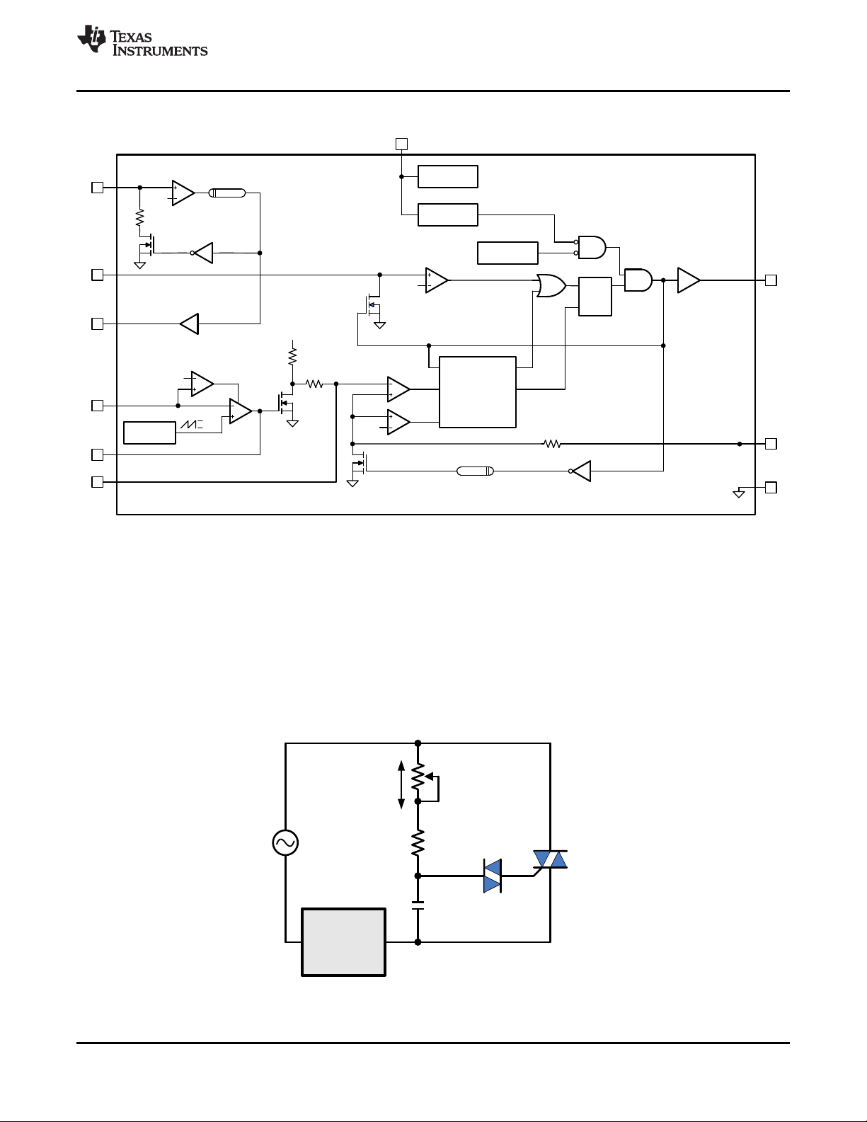
SIMPLIFIED INTERNAL BLOCK DIAGRAM
Figure 11. Simplified Block Diagram
APPLICATION INFORMATION
FUNCTIONAL DESCRIPTION
The LM3445 contains all the necessary circuitry to build a line-powered (mains powered) constant current LED
driver whose output current can be controlled with a conventional triac dimmer.
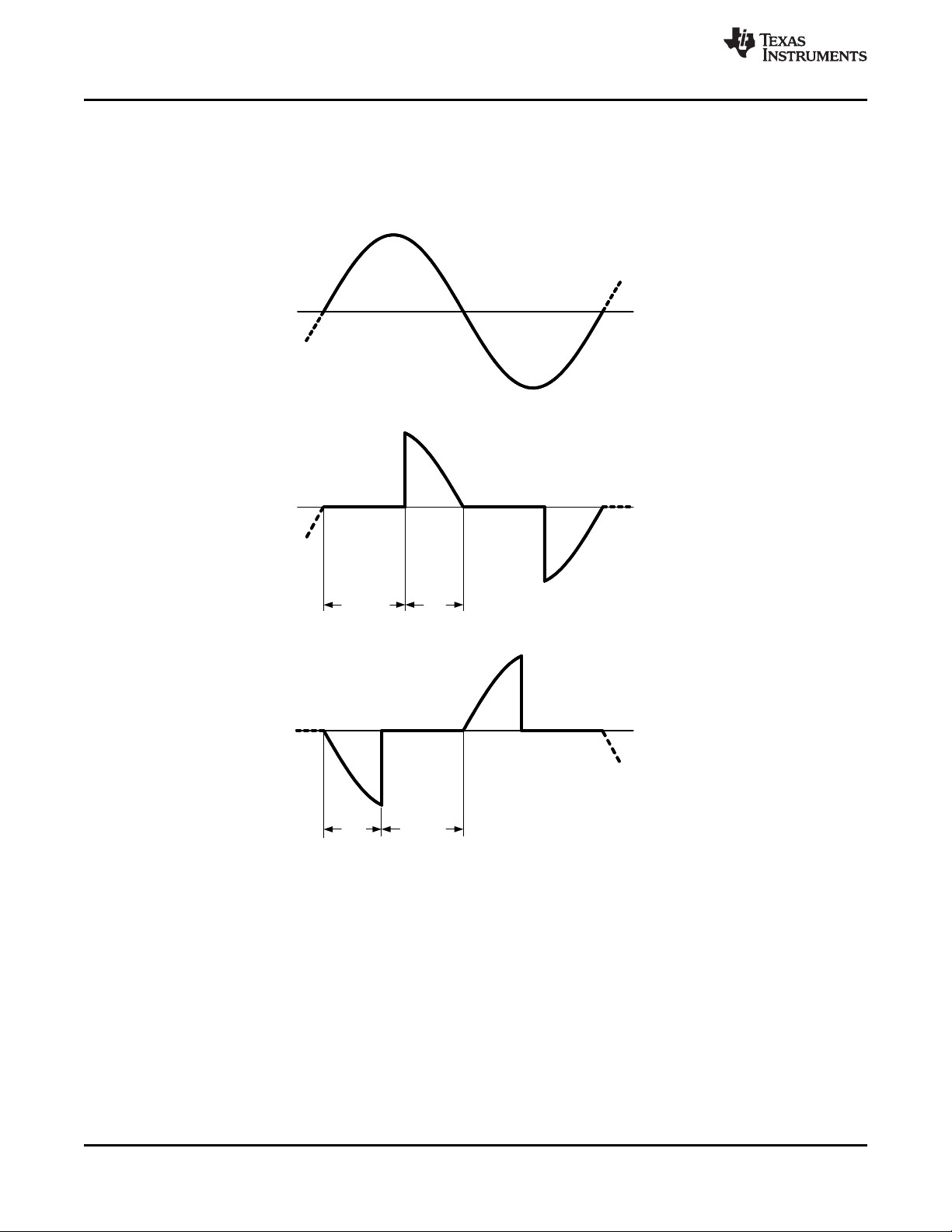
OVERVIEW OF PHASE CONTROL DIMMING
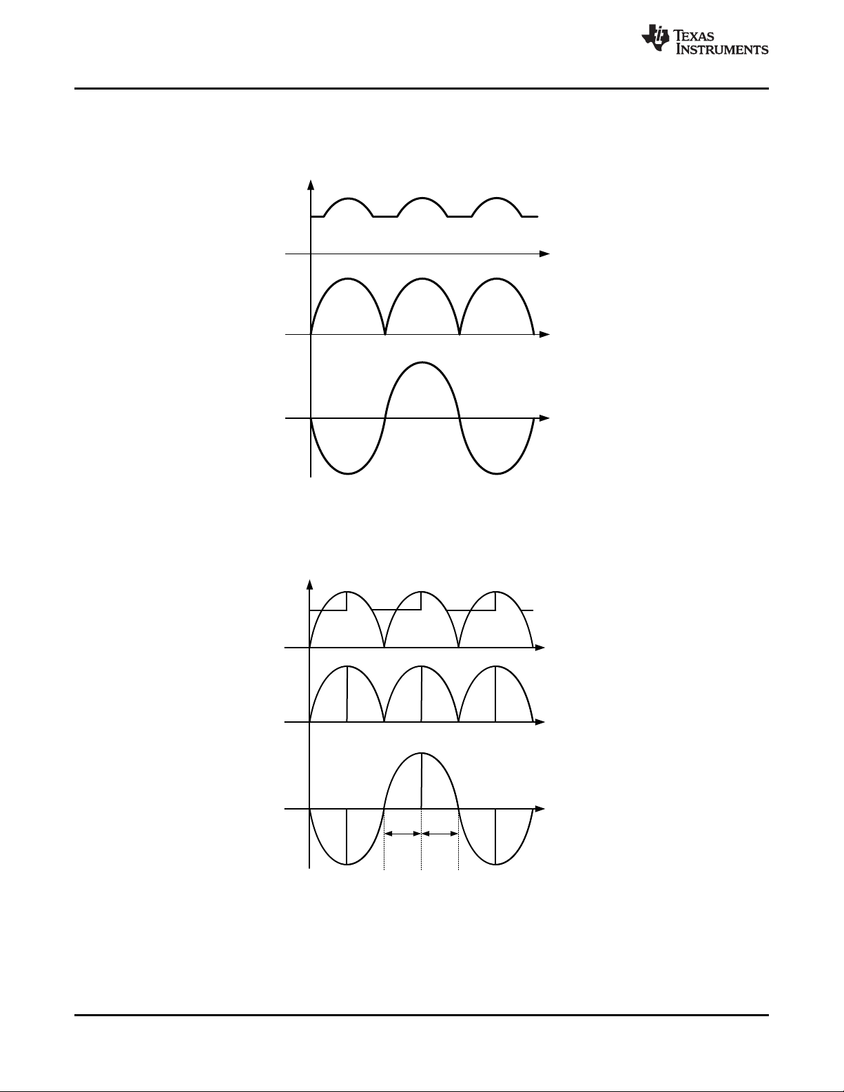
A basic "phase controlled" triac dimmer circuit is shown in Figure 12.
Copyright © 2009–2013, Texas Instruments Incorporated Submit Documentation Feedback 7
Figure 12. Basic Triac Dimmer
Product Folder Links: LM3445
Page 8
DELAY
DELAY
(a)
(b)
(c)
?
?
LM3445
SNVS570L –JANUARY 2009–REVISED MAY 2013
www.ti.com
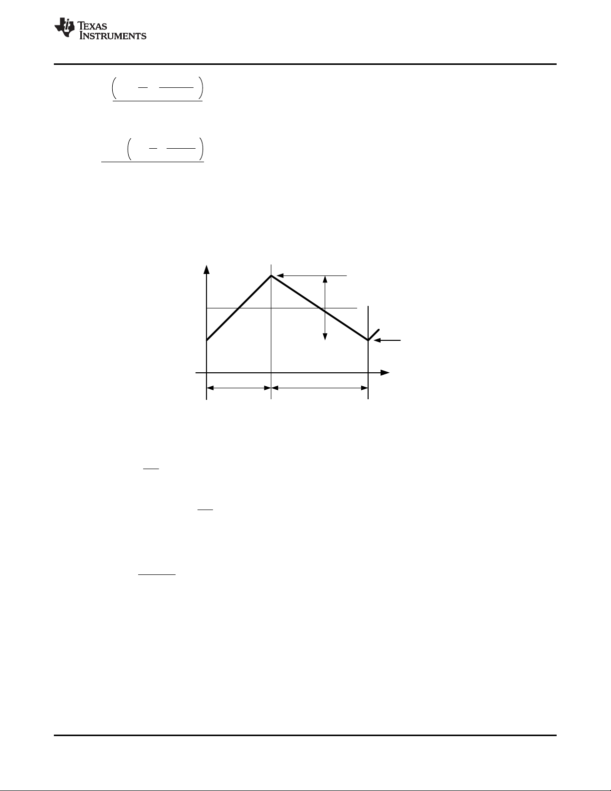
An RC network consisting of R1, R2, and C1 delay the turn on of the triac until the voltage on C1 reaches the
trigger voltage of the diac. Increasing the resistance of the potentiometer (wiper moving downward) increases the
turn-on delay which decreases the on-time or "conduction angle" of the triac (θ). This reduces the average power
delivered to the load. Voltage waveforms for a simple triac dimmer are shown in Figure 13. Figure 13a shows the
full sinusoid of the input voltage. Even when set to full brightness, few dimmers will provide 100% on-time, i.e.,
the full sinusoid.
Figure 13. Line Voltage and Dimming Waveforms
Figure 13b shows a theoretical waveform from a dimmer. The on-time is often referred to as the "conduction
angle" and may be stated in degrees or radians. The off-time represents the delay caused by the RC circuit
feeding the triac. The off-time be referred to as the "firing angle" and is simply 180° - θ.
Figure 13c shows a waveform from a so-called reverse phase dimmer, sometimes referred to as an electronic
dimmer. These typically are more expensive, microcontroller based dimmers that use switching elements other
than triacs. Note that the conduction starts from the zero-crossing, and terminates some time later. This method
of control reduces the noise spike at the transition.
Since the LM3445 has been designed to assess the relative on-time and control the LED current accordingly,
most phase-control dimmers, both forward and reverse phase, may be used with success.
8 Submit Documentation Feedback Copyright © 2009–2013, Texas Instruments Incorporated
Product Folder Links: LM3445
Page 9
I
COLL
V+
BR1
VAC
TRIAC
DIMMER
+
+
1
2
3
4
5 6
7
8
9
10
-
V
LED
GND
VCC
FLTR2
ASNS
FLTR1
ISNS
GATE
BLDR
COFF
DIM
LM3445MM
V
LED-
D3
C7
C9
C10
D4
D8
D9
R2
D1
Q1
C5
R5
C12
D2
D10
Q2
L2
Q3
R3
R4
C11
C4
C3
R1
U1
V
BUCK
LM3445
www.ti.com
SNVS570L –JANUARY 2009–REVISED MAY 2013
THEORY OF OPERATION
Refer to Figure 14 which shows the LM3445 along with basic external circuitry.
Figure 14. LM3445 Schematic
Copyright © 2009–2013, Texas Instruments Incorporated Submit Documentation Feedback 9
Product Folder Links: LM3445
Page 10
delay
V
BUCK
V
AC
V
BR1
t
?
(a)
(b)
(c)
t
t
V
AC
V
BR1
t
(a)
(b)
(c)
V
BUCK
LM3445
SNVS570L –JANUARY 2009–REVISED MAY 2013
www.ti.com
SENSING THE RECTIFIED TRIAC WAVEFORM
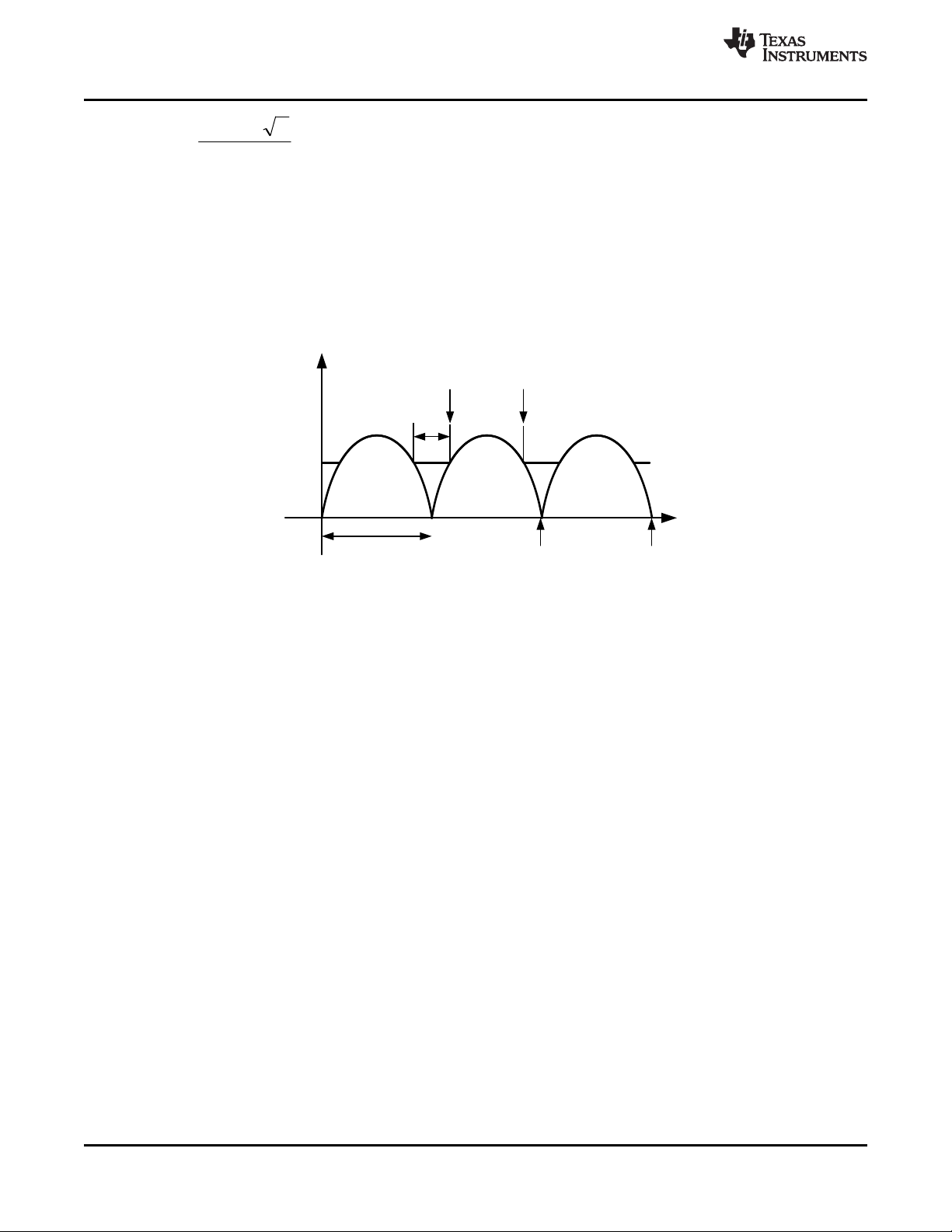
A bridge rectifier, BR1, converts the line (mains) voltage (Figure 15c) into a series of half-sines as shown in
Figure 15b. Figure 15a shows a typical voltage waveform after diode D3 (valley fill circuit, or V
BUCK
).
Figure 15. Voltage Waveforms After Bridge Rectifier Without Triac Dimming
Figure 16c and Figure 16b show typical triac dimmed voltage waveforms before and after the bridge rectifier.
Figure 16a shows a typical triac dimmed voltage waveform after diode D3 (valley fill circuit, or V
Figure 16. Voltage Waveforms After Bridge Rectifier With Triac Dimming
BUCK
).
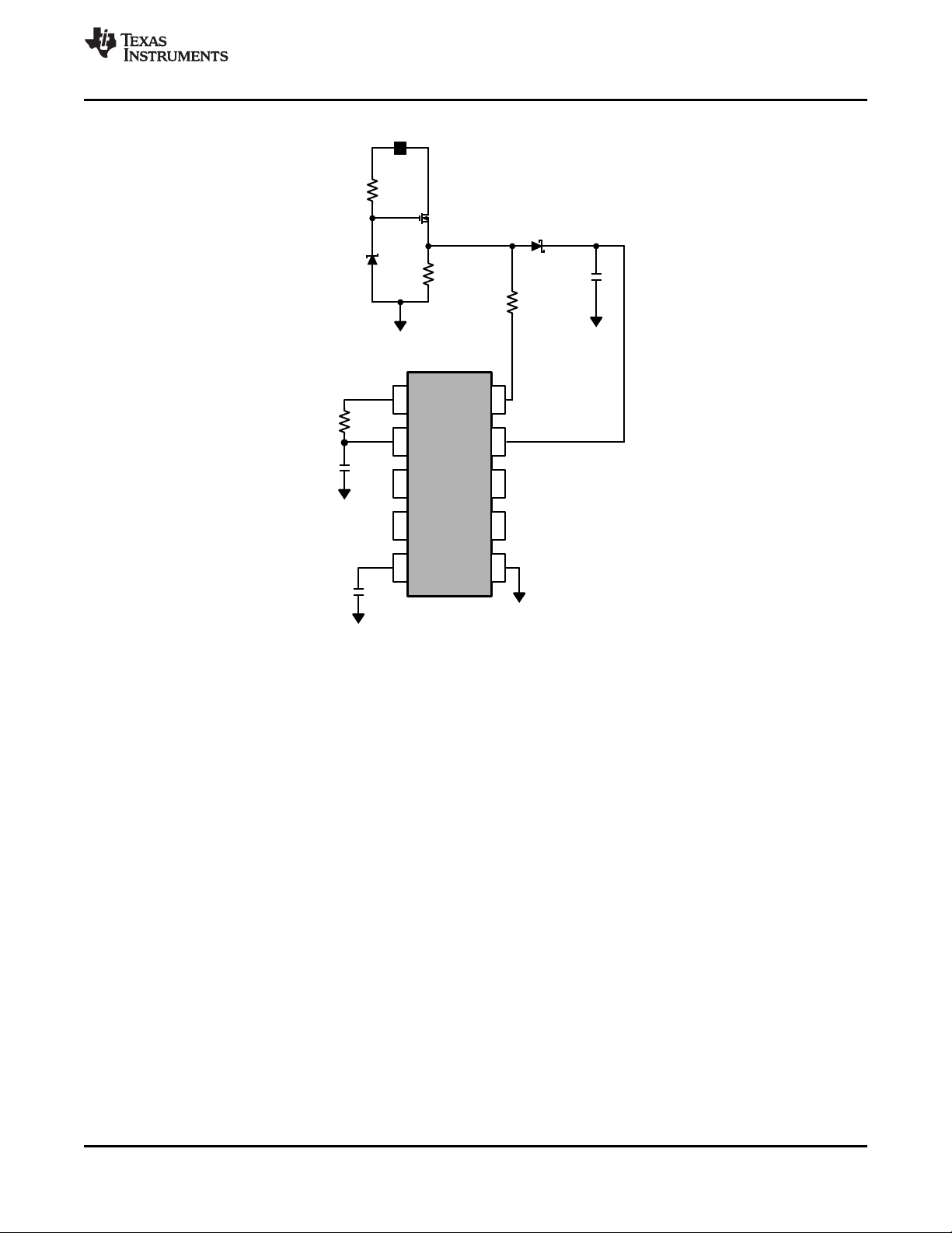
LM3445 LINE SENSING CIRCUITRY
An external series pass regulator (R2, D1, and Q1) translates the rectified line voltage to a level where it can be
sensed by the BLDR pin on the LM3445.
10 Submit Documentation Feedback Copyright © 2009–2013, Texas Instruments Incorporated
Product Folder Links: LM3445
Page 11
1
2
3
4
5 6
7
8
9
10
GND
VCC
FLTR2
ASNS
FLTR1
ISNS
GATE
BLDR
COFF
DIM
LM3445MM
V+
D1
D2
R2
Q1
R5 C5
U1
C4
C3
R1
R11
LM3445
www.ti.com
SNVS570L –JANUARY 2009–REVISED MAY 2013
Figure 17. LM3445 AC Line Sense Circuitry
D1 is typically a 15V zener diode which forces transistor Q1 to “stand-off” most of the rectified line voltage.
Having no capacitance on the source of Q1 allows the voltage on the BLDR pin to rise and fall with the rectified
line voltage as the line voltage drops below zener voltage D1 (see ANGLE DETECT).
A diode-capacitor network (D2, C5) is used to maintain the voltage on the VCC pin while the voltage on the
BLDR pin goes low. This provides the supply voltage to operate the LM3445.
Resistor R5 is used to bleed charge out of any stray capacitance on the BLDR node and may be used to provide
the necessary holding current for the dimmer when operating at light output currents.
TRIAC HOLDING CURRENT RESISTOR
In order to emulate an incandescent light bulb (essentially a resistor) with any LED driver, the existing triac will
require a small amount of holding current throughout the AC line cycle. An external resistor (R5) needs to be
placed on the source of Q1 to GND to perform this function. Most existing triac dimmers only require a few
milliamps of current to hold them on. A few “less expensive” triacs sold on the market will require a bit more
current. The value of resistor R5 will depend on:
• What type of triac the LM3445 will be used with
• How many light fixtures are running off of the triac
With a single LM3445 circuit on a common triac dimmer, a holding current resistor between 3 kΩ and 5 kΩ will
be required. As the number of LM3445 circuits is added to a single dimmer, the holding resistor R5’s resistance
can be increased. A few triac dimmers will require a resistor as low as 1 kΩ or lower for a single LM3445 circuit.
The trade-off will be performance vs efficiency. As the holding resistor R5 is increased, the overall efficiency per
LM3445 will also increase.
Copyright © 2009–2013, Texas Instruments Incorporated Submit Documentation Feedback 11
Product Folder Links: LM3445
Page 12

LM3445
SNVS570L –JANUARY 2009–REVISED MAY 2013
www.ti.com
ANGLE DETECT
The Angle Detect circuit uses a comparator with a fixed threshold voltage of 7.21V to monitor the BLDR pin to
determine whether the triac is on or off. The output of the comparator drives the ASNS buffer and also controls
the Bleeder circuit. A 4 µs delay line on the output is used to filter out noise that could be present on this signal.
The output of the Angle Detect circuit is limited to a 0V to 4.0V swing by the buffer and presented to the ASNS
pin. R1 and C3 comprise a low-pass filter with a bandwidth on the order of 1.0Hz.
The Angle Detect circuit and its filter produce a DC level which corresponds to the duty cycle (relative on-time) of
the triac dimmer. As a result, the LM3445 will work equally well with 50Hz or 60Hz line voltages.
BLEEDER
While the BLDR pin is below the 7.21V threshold, the bleeder MOSFET is on to place a small load (230Ω) on the
series pass regulator. This additional load is necessary to complete the circuit through the triac dimmer so that
the dimmer delay circuit can operate correctly. Above 7.21V, the bleeder resistor is removed to increase
efficiency.
FLTR1 PIN
The FLTR1 pin has two functions. Normally, it is fed by ASNS through filter components R1 and C3 and drives
the dim decoder. However, if the FLTR1 pin is tied above 4.9V (typical), e.g., to VCC, the Ramp Comparator is
tri-stated, disabling the dim decoder. See MASTER/SLAVE OPERATION.
DIM DECODER
The ramp generator produces a 5.85 kHz saw tooth wave with a minimum of 1.0V and a maximum of 3.0V. The
filtered ASNS signal enters pin FLTR1 where it is compared against the output of the Ramp Generator.
The output of the ramp comparator will have an on-time which is inversely proportional to the average voltage
level at pin FLTR1. However, since the FLTR1 signal can vary between 0V and 4.0V (the limits of the ASNS pin),
and the Ramp Generator signal only varies between 1.0V and 3.0V, the output of the ramp comparator will be on
continuously for V
135° to provide a 0 – 100% dimming range.
The output of the ramp comparator drives both a common-source N-channel MOSFET through a Schmitt trigger
and the DIM pin (see MASTER/SLAVE OPERATION for further functions of the DIM pin). The MOSFET drain is
pulled up to 750 mV by a 50 kΩ resistor.
Since the MOSFET inverts the output of the ramp comparator, the drain voltage of the MOSFET is proportional
to the duty cycle of the line voltage that comes through the triac dimmer. The amplitude of the ramp generator
causes this proportionality to "hard limit" for duty cycles above 75% and below 25%.
The MOSFET drain signal next passes through an RC filter comprised of an internal 370 kΩ resistor, and an
external capacitor on pin FLTR2. This forms a second low pass filter to further reduce the ripple in this signal,
which is used as a reference by the PWM comparator. This RC filter is generally set to 10Hz.
The net effect is that the output of the dim decoder is a DC voltage whose amplitude varies from near 0V to 750
mV as the duty cycle of the dimmer varies from 25% to 75%. This corresponds to conduction angles of 45° to
135°, respectively.
The output voltage of the Dim Decoder directly controls the peak current that will be delivered by Q2 during its
on-time. See BUCK CONVERTER for details.
As the triac fires beyond 135°, the DIM decoder no longer controls the dimming. At this point the LEDs will dim
gradually for one of two reasons:
1. The voltage at V
decrease as V
2. Minimum on-time is reached which fixes the duty-cycle and therefore reduces the voltage at V
The transition from dimming with the DIM decoder to headroom or minimum on-time dimming is seamless. LED
currents from full load to as low as 0.5 mA can be easily achieved.
< 1.0V and off continuously for V
FLTR1
decreases and the buck converter runs out of headroom and causes LED current to
BUCK
decreases.
BUCK
> 3.0V. This allows a decoding range from 45° to
FLTR1
BUCK
.
12 Submit Documentation Feedback Copyright © 2009–2013, Texas Instruments Incorporated
Product Folder Links: LM3445
Page 13

+
+
D3
C7
C9
C10
D4
D8
V
BUCK
V+
+
-
+
-
2
V
BUCK
2
V
BUCK
+
+
+
D3
C7
C8
C9
C10
D4
D5
D6
D7
D8
R7
R8
D9
R6
V
BUCK
V+
+
+
D3
C7
C9
C10
D4
D8
D9
R7
R6
R8
V
BUCK
V+
LM3445
www.ti.com
SNVS570L –JANUARY 2009–REVISED MAY 2013
VALLEY-FILL CIRCUIT
V
supplies the power which drives the LED string. Diode D3 allows V
BUCK
and off. V
has a relatively small hold capacitor C10 which reduces the voltage ripple when the valley fill
BUCK
capacitors are being charged. However, the network of diodes and capacitors shown between D3 and C10 make
up a "valley-fill" circuit. The valley-fill circuit can be configured with two or three stages. The most common
configuration is two stages. Figure 18 illustrates a two and three stage valley-fill circuit.
Figure 18. Two and Three Stage Valley Fill Circuit
The valley-fill circuit allows the buck regulator to draw power throughout a larger portion of the AC line. This
allows the capacitance needed at V
to be lower than if there were no valley-fill circuit, and adds passive
BUCK
power factor correction (PFC) to the application. Besides better power factor correction, a valley-fill circuit allows
the buck converter to operate while separate circuitry translates the dimming information. This allows for dimming
that isn’t subject to 120Hz flicker that can be perceived by the human eye.
to remain high while V+ cycles on
BUCK
VALLEY-FILL OPERATION
When the “input line is high”, power is derived directly through D3. The term “input line is high” can be explained
as follows. The valley-fill circuit charges capacitors C7 and C9 in series (see Figure 19) when the input line is
high.
Copyright © 2009–2013, Texas Instruments Incorporated Submit Documentation Feedback 13
Figure 19. Two Stage Valley-Fill Circuit When AC Line is High
Product Folder Links: LM3445
Page 14

V
VF-CAP
=
2
V
AC-RMS
3
+
+
D3
C7
C9
C10
D4
D8
D9
V
BUCK
V+
+
-
+
-
V
BUCK
V
BUCK
V
VF-CAP
=
2
V
AC-RMS
LM3445
SNVS570L –JANUARY 2009–REVISED MAY 2013
www.ti.com
The peak voltage of a two stage valley-fill capacitor is:
(1)
As the AC line decreases from its peak value every cycle, there will be a point where the voltage magnitude of
the AC line is equal to the voltage that each capacitor is charged. At this point diode D3 becomes reversed
biased, and the capacitors are placed in parallel to each other (Figure 20), and V
equals the capacitor
BUCK
voltage.
Figure 20. Two Stage Valley-Fill Circuit When AC Line is Low
A three stage valley-fill circuit performs exactly the same as two-stage valley-fill circuit except now three
capacitors are now charged in series, and when the line voltage decreases to:
Diode D3 is reversed biased and three capacitors are in parallel to each other.
The valley-fill circuit can be optimized for power factor, voltage hold up and overall application size and cost. The
LM3445 will operate with a single stage or a three stage valley-fill circuit as well. Resistor R8 functions as a
current limiting resistor during start-up, and during the transition from series to parallel connection. Resistors R6
and R7 are 1 MΩ bleeder resistors, and may or may not be necessary for each application.
BUCK CONVERTER
The LM3445 is a buck controller that uses a proprietary constant off-time method to maintain constant current
through a string of LEDs. While transistor Q2 is on, current ramps up through the inductor and LED string. A
resistor R3 senses this current and this voltage is compared to the reference voltage at FLTR2. When this
sensed voltage is equal to the reference voltage, transistor Q2 is turned off and diode D10 conducts the current
through the inductor and LEDs. Capacitor C12 eliminates most of the ripple current seen in the inductor. Resistor
R4, capacitor C11, and transistor Q3 provide a linear current ramp that sets the constant off-time for a given
output voltage.
(2)
Product Folder Links: LM3445
14 Submit Documentation Feedback Copyright © 2009–2013, Texas Instruments Incorporated
Page 15

= D =
t
ON
t
ON
+ t
OFF
= tON x f
SW
V
O
V
IN
L2
R3
C11
Q2
Q3
D10
I
COLL
4
6
7
8
R4
GND
ISNS
GATE
COFF
LM3445MM
V
BUCK
C12
LM3445
www.ti.com
SNVS570L –JANUARY 2009–REVISED MAY 2013
Figure 21. LM3445 Buck Regulation Circuit
OVERVIEW OF CONSTANT OFF-TIME CONTROL
A buck converter’s conversion ratio is defined as:
Constant off-time control architecture operates by simply defining the off-time and allowing the on-time, and
therefore the switching frequency, to vary as either VINor VOchanges. The output voltage is equal to the LED
string voltage (V
), and should not change significantly for a given application. The input voltage or V
LED
BUCK
(3)
in
this analysis will vary as the input line varies. The length of the on-time is determined by the sensed inductor
current through a resistor to a voltage reference at a comparator. During the on-time, denoted by tON, MOSFET
switch Q2 is on causing the inductor current to increase. During the on-time, current flows from V
the LEDs, through L2, Q2, and finally through R3 to ground. At some point in time, the inductor current reaches a
maximum (I
) determined by the voltage sensed at R3 and the ISNS pin. This sensed voltage across R3 is
L2-PK
BUCK
, through
compared against the voltage of dim decoder output, FLTR2, at which point Q2 is turned off by the controller.
Copyright © 2009–2013, Texas Instruments Incorporated Submit Documentation Feedback 15
Product Folder Links: LM3445
Page 16

t
t
OFF
t
ON
L2
(t)
I
AVE
I
L2-PK
'i
L
I
L2-MIN
LM3445
SNVS570L –JANUARY 2009–REVISED MAY 2013
www.ti.com
Figure 22. Inductor Current Waveform in CCM
During the off-period denoted by t
, the current through L2 continues to flow through the LEDs via D10.
OFF
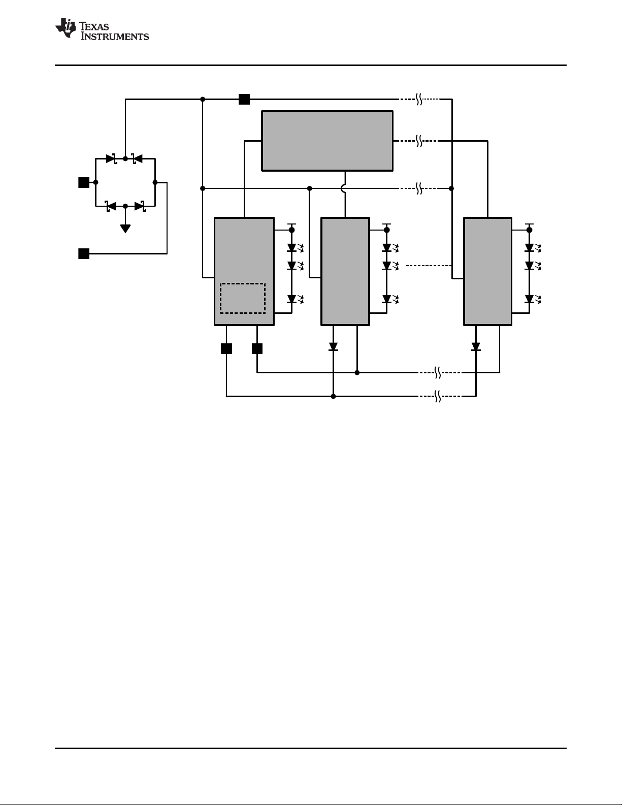
MASTER/SLAVE OPERATION
Multiple LM3445s can be configured so that large strings of LEDs can be controlled by a single triac dimmer. By
doing so, smooth consistent dimming for multiple LED circuits is achieved.
When the FLTR1 pin is tied above 4.9V (typical), preferably to VCC, the ramp comparator is tri-stated, disabling
the dim decoder. This allows one or more LM3445 devices or PWM LED driver devices (slaves) to be controlled
by a single LM3445 (master) by connecting their DIM pins together.
MASTER/SLAVE CONFIGURATION
TI offers an LM3445 demonstration PCB for customer evaluation through our website. The following description
and theory uses reference designators that follow our evaluation PCB. The LM3445 Master/Slave schematics are
illustrated below (Figure 23 through Figure 25) for clarity. Each board contains a separate circuit for the Master
and Slave function. Both the Master and Slave boards will need to be modified from their original stand alone
function so that they can be coupled together. Only the Master LM3445 requires use of the Master/Slave circuit
for any number of slaves.
MASTER BOARD MODIFICATIONS
• Remove R10 and replace with a BAS40 diode
• Connect TP18 to TP14 (VCC)
• Connect TP17 (gate of Q5) to TP15 (gate of Q2)
SLAVE BOARD(S) MODIFICATIONS
• Remove R11 (disconnects BLDR)
• Tie TP14 (FLTR1) to V
CC
MASTER/SLAVE(S) INTERCONNECTION
• Connect TP19 of Master to TP10 of Slave (Master VCC Control)
• Connect TP6 (DIM pin) of Master to TP6 (DIM pin) of Slave (Master DIM Control)
MASTER/SLAVE THEORY OF OPERATION
By placing two series diodes on the Master VCC circuit one forces the master VCC UVLO to become the
dominant threshold. When Master VCC drops below UVLO, GATE stops switching and the RC timer (>200 µs)
rises above the TL431 threshold (2.5V) which in turn pulls down on the gate of the Slave pass device (Q1).
The valley-fill circuit could consist of one large circuit to power all LM3445 series connected, or each LM3445
circuit could have a separate valley-fill circuit located near the buck converter.
16 Submit Documentation Feedback Copyright © 2009–2013, Texas Instruments Incorporated
Product Folder Links: LM3445
Page 17

1
2
3
4
5 6
7
8
9
10
GND
VCC
FLTR2
ASNS
FLTR1
ISNS
GATE
BLDR
COFF
DIM
LM3445MM
V+
D1
D2
R2
Q1
R5
C5
U1
C4
C3
R1
R11
Q5
R12
R13
C14
C13
BAS40
1
2
3
4
5 6
7
8
9
10
GND
VCC
FLTR2
ASNS
FLTR1
ISNS
GATE
BLDR
COFF
DIM
LM3445MM
V+
D1
D2
R2
Q1
R5
C5
U1
C4
R11
MASTER-
BUCK
SLAVE
BUCK
R10
MASTER LM3445 SLAVE LM3445
MASTER-V
BUCK
SLAVE-V
BUCK
MASTER/
SLAVE
CIRCUIT
MASTER
DIM CTRL
MASTER
VCC CTRL
TP18 TP19
TP10
TP17
D11
LM3445
www.ti.com
MASTER/SLAVE CONNECTION DIAGRAM
SNVS570L –JANUARY 2009–REVISED MAY 2013
Figure 23. Master Slave Configuration
Copyright © 2009–2013, Texas Instruments Incorporated Submit Documentation Feedback 17
Product Folder Links: LM3445
Page 18

SLAVE
BUCK
V+
BR1
SLAVE
BUCK
Valley-Fill
CKT
Valley-Fill
CKT
Valley-Fill
CKT
N
L
MASTER
DIM
MASTER
CTRL
MASTER
BUCK
MASTER
VCC
LM3445
SNVS570L –JANUARY 2009–REVISED MAY 2013
MASTER/SLAVE BLOCK DIAGRAMS
www.ti.com
Figure 24. Master/Slave Configuration With Separate Valley-Fill Circuits
18 Submit Documentation Feedback Copyright © 2009–2013, Texas Instruments Incorporated
Product Folder Links: LM3445
Page 19
SLAVE
BUCK
V+
BR1
SLAVE
BUCK
N
L
MASTER
CTRL
MASTER
BUCK
MASTER
VCC CTRL
MASTER
DIM CTRL
Large Valley-Fill CKT
LM3445
www.ti.com
SNVS570L –JANUARY 2009–REVISED MAY 2013
Figure 25. Master/Slave Configuration With One Valley-Fill Circuit
THERMAL SHUTDOWN
Thermal shutdown limits total power dissipation by turning off the output switch when the IC junction temperature
exceeds 165°C. After thermal shutdown occurs, the output switch doesn’t turn on until the junction temperature
drops to approximately 145°C.
Copyright © 2009–2013, Texas Instruments Incorporated Submit Documentation Feedback 19
Product Folder Links: LM3445
Page 20

1
K
V
LED
V
BUCK
u
¸
¹
·
¨
©
§
fSW =
1
t
OFF
V
LED
= K u
D
V
BUCK
D
t
ON
f
SW
=
,
and
1 - D
t
OFF
f
SW
=
1
t
OFF
+ t
ON
f
SW
=
D =
t
ON
t
ON
+ t
OFF
=
V
LED
V
BUCK
'¶=
t
OFF
t
ON
+ t
OFF
t
OFF
= C11 x 1.276V x
R4
V
LED
dv
dt
= D
1
V
LED
V
BUCK
u
= D =
t
ON
t
ON
+ t
OFF
= t
ON
x f
SW
V
LED
V
BUCK
LM3445
SNVS570L –JANUARY 2009–REVISED MAY 2013
www.ti.com
DESIGN GUIDE
DETERMINING DUTY-CYCLE (D)
Duty cycle (D) approximately equals:
(4)
With efficiency considered:
(5)
For simplicity, choose efficiency between 75% and 85%.
CALCULATING OFF-TIME
The “Off-Time” of the LM3445 is set by the user and remains fairly constant as long as the voltage of the LED
stack remains constant. Calculating the off-time is the first step in determining the switching frequency of the
converter, which is integral in determining some external component values.
PNP transistor Q3, resistor R4, and the LED string voltage define a charging current into capacitor C11. A
constant current into a capacitor creates a linear charging characteristic.
(6)
Resistor R4, capacitor C11 and the current through resistor R4 (i
are all fixed. Therefore, dv is fixed and linear, and dt (t
) can now be calculated.
OFF
), which is approximately equal to V
COLL
LED
/R4,
Common equations for determining duty cycle and switching frequency in any buck converter:
Therefore:
With efficiency of the buck converter in mind:
Substitute equations and rearrange:
Off-time, and switching frequency can now be calculated using the equations above.
(7)
(8)
(9)
(10)
(11)
SETTING THE SWITCHING FREQUENCY
Selecting the switching frequency for nominal operating conditions is based on tradeoffs between efficiency
(better at low frequency) and solution size/cost (smaller at high frequency).
20 Submit Documentation Feedback Copyright © 2009–2013, Texas Instruments Incorporated
Product Folder Links: LM3445
Page 21

BUCK(MAX)
= V
AC-RMS(MAX)
x
2
V
LED(MIN)
t
ON(MIN)
=
V
BUCK(MAX)
f
SW
1
K
1
u
V
BUCK
(V)
NORMALIZED SW FREQ
1.50
1.25
1.00
0.75
0.50
0.25
0 50 100 150 200
3 LEDs
5 LEDs
7 LEDs
9 LEDs
Series
connected LEDs
LM3445
www.ti.com
The input voltage to the buck converter (V
) changes with both line variations and over the course of each
BUCK
SNVS570L –JANUARY 2009–REVISED MAY 2013
half-cycle of the input line voltage. The voltage across the LED string will, however, remain constant, and
therefore the off-time remains constant.
The on-time, and therefore the switching frequency, will vary as the V
voltage changes with line voltage. A
BUCK
good design practice is to choose a desired nominal switching frequency knowing that the switching frequency
will decrease as the line voltage drops and increase as the line voltage increases (see Figure 26).
Figure 26. Graphical Illustration of Switching Frequency vs V
BUCK
The off-time of the LM3445 can be programmed for switching frequencies ranging from 30 kHz to over 1 MHz. A
trade-off between efficiency and solution size must be considered when designing the LM3445 application.
The maximum switching frequency attainable is limited only by the minimum on-time requirement (200 ns).
Worst case scenario for minimum on time is when V
string voltage (V
) is at its minimum value.
LED
is at its maximum voltage (AC high line) and the LED
BUCK
The maximum voltage seen by the Buck Converter is:
INDUCTOR SELECTION
The controlled off-time architecture of the LM3445 regulates the average current through the inductor (L2), and
therefore the LED string current. The input voltage to the buck converter (V
over the course of each half-cycle of the input line voltage. The voltage across the LED string is relatively
constant, and therefore the current through R4 is constant. This current sets the off-time of the converter and
therefore the output volt-second product (V
x off-time) remains constant. A constant volt-second product
LED
makes it possible to keep the ripple through the inductor constant as the voltage at V
) changes with line variations and
BUCK
varies.
BUCK
(12)
(13)
Copyright © 2009–2013, Texas Instruments Incorporated Submit Documentation Feedback 21
Product Folder Links: LM3445
Page 22

t
OFF
x
V
LED
'i
'i #
t
OFF
x
V
LED
V
L(OFF-TIME)
= V
LED
= L x
'i
't
V
L(OFF-TIME)
= V
LED
= L x
(I
(MAX)
- I
(MIN)
)
't
di
dt
-
C12
R3
Q2
-
D10
V
LED
V
BUCK
V
L2
L2
LM3445
SNVS570L –JANUARY 2009–REVISED MAY 2013
Figure 27. LM3445 External Components of the Buck Converter
www.ti.com
The equation for an ideal inductor is:
Given a fixed inductor value, L, this equation states that the change in the inductor current over time is
proportional to the voltage applied across the inductor.
During the on-time, the voltage applied across the inductor is,
V
L(ON-TIME)
= V
BUCK
- (V
LED
+ V
+ IL2x R3) (15)
DS(Q2)
Since the voltage across the MOSFET switch (Q2) is relatively small, as is the voltage across sense resistor R3,
we can simplify this to approximately,
V
L(ON-TIME)
= V
BUCK
- V
LED
During the off-time, the voltage seen by the inductor is approximately:
V
L(OFF-TIME)
The value of V
= V
LED
L(OFF-TIME)
will be relatively constant, because the LED stack voltage will remain constant. If we
rewrite the equation for an inductor inserting what we know about the circuit during the off-time, we get:
Re-arranging this gives:
From this we can see that the ripple current (Δi) is proportional to off-time (t
dominated by V
LED
divided by a constant (L2).
) multiplied by a voltage which is
OFF
These equations can be rearranged to calculate the desired value for inductor L2.
Where:
22 Submit Documentation Feedback Copyright © 2009–2013, Texas Instruments Incorporated
Product Folder Links: LM3445
(14)
(16)
(17)
(18)
(19)
(20)
Page 23
L-PK(UNDIM)
=
750 mV
R3
AVE(UNDIM)
= I
L2-PK(UNDIM)
-
'i
L
L2-PK
= I
AVE
+
'i
L
t
t
OFF
t
ON
L2
(t)
I
AVE
I
L2-PK
'i
L
I
L2-MIN
f
SW
x 'i
V
LED
V
LED
V
BUCK
1
K
1
u
V
LED
t
OFF
=
V
BUCK
f
SW
1
K
1
u
LM3445
www.ti.com
SNVS570L –JANUARY 2009–REVISED MAY 2013
(21)
Finally:
(22)
Refer to DESIGN EXAMPLE to better understand the design process.
SETTING THE LED CURRENT
The LM3445 constant off-time control loop regulates the peak inductor current (IL2). The average inductor current
equals the average LED current (I
inductor current.
). Therefore the average LED current is regulated by regulating the peak
AVE
Figure 28. Inductor Current Waveform in CCM
Knowing the desired average LED current, I
and the nominal inductor current ripple, ΔiL, the peak current for
AVE
an application running in continuous conduction mode (CCM) is defined as follows:
(23)
Or, the maximum, or "undimmed", LED current would then be,
(24)
This is important to calculate because this peak current multiplied by the sense resistor R3 will determine when
the internal comparator is tripped. The internal comparator turns the control MOSFET off once the peak sensed
voltage reaches 750 mV.
(25)
Current Limit: Under normal circumstances, the trip voltage on the PWM comparator would be less than or
equal to 750 mV, depending on the amount of dimming. However, if there is a short circuit or an excessive load
on the output, higher than normal switch currents will cause a voltage above 1.27V on the ISNS pin which will
trip the I-LIM comparator. The I-LIM comparator will reset the RS latch, turning off Q2. It will also inhibit the Start
Pulse Generator and the COFF comparator by holding the COFF pin low. A delay circuit will prevent the start of
another cycle for 180 µs.
VALLEY FILL CAPACITORS
Determining voltage rating and capacitance value of the valley-fill capacitors:
The maximum voltage seen by the valley-fill capacitors is:
Copyright © 2009–2013, Texas Instruments Incorporated Submit Documentation Feedback 23
Product Folder Links: LM3445
Page 24
V
BUCK
8.33 ms
30°
t
X
t
150°
180°0°
VF-CAP
=
2
V
AC(MAX)
#stages
LM3445
SNVS570L –JANUARY 2009–REVISED MAY 2013
www.ti.com
(26)
This is, of course, if the capacitors chosen have identical capacitance values and split the line voltage equally.
Often a 20% difference in capacitance could be observed between like capacitors. Therefore a voltage rating
margin of 25% to 50% should be considered.
Determining the capacitance value of the valley-fill capacitors:
The valley fill capacitors should be sized to supply energy to the buck converter (V
) when the input line is
BUCK
less than its peak divided by the number of stages used in the valley fill (tX). The capacitance value should be
calculated when the triac is not firing, i.e. when full LED current is being drawn by the LED string. The maximum
power is delivered to the LED string at this time, and therefore the most capacitance will be needed.
Figure 29. Two Stage Valley-Ffill V
Voltage with no TRIAC Dimming
BUCK
From the above illustration and the equation for current in a capacitor, i = C x dV/dt, the amount of capacitance
needed at V
At 60Hz, and a valley-fill circuit of two stages, the hold up time (tX) required at V
will be calculated as follows:
BUCK
is calculated as follows. The
BUCK
total angle of an AC half cycle is 180° and the total time of a half AC line cycle is 8.33 ms. When the angle of the
AC waveform is at 30° and 150°, the voltage of the AC line is exactly ½ of its peak. With a two stage valley-fill
circuit, this is the point where the LED string switches from power being derived from AC line to power being
derived from the hold up capacitors (C7 and C9). 60° out of 180° of the cycle or 1/3 of the cycle the power is
derived from the hold up capacitors (1/3 x 8.33 ms = 2.78 ms). This is equal to the hold up time (dt) from the
above equation, and dv is the amount of voltage the circuit is allowed to droop. From the next section
(“Determining Maximum Number of Series Connected LEDs Allowed”) we know the minimum V
BUCK
voltage will
be about 45V for a 90VACto 135VACline. At 90VAClow line operating condition input, ½ of the peak voltage is
64V. Therefore with some margin the voltage at V
(P
OUT/VBUCK
), where P
is equal to (V
OUT
LED
x I
LED
can not droop more than about 15V (dv). (i) is equal to
BUCK
). Total capacitance (C7 in parallel with C9) can now be
calculated. See DESIGN EXAMPLE for further calculations of the valley-fill capacitors.
Determining Maximum Number of Series Connected LEDs Allowed:
The LM3445 is an off-line buck topology LED driver. A buck converter topology requires that the input voltage
(V
) of the output circuit must be greater than the voltage of the LED stack (V
BUCK
) for proper regulation. One
LED
must determine what the minimum voltage observed by the buck converter will be before the maximum number
of LEDs allowed can be determined. Two variables will have to be determined in order to accomplish this.
1. AC line operating voltage. This is usually 90VACto 135VACfor North America. Although the LM3445 can
operate at much lower and higher input voltages a range is needed to illustrate the design process.
2. How many stages are implemented in the valley-fill circuit (1, 2 or 3).
In this example the most common valley-fill circuit will be used (two stages).
24 Submit Documentation Feedback Copyright © 2009–2013, Texas Instruments Incorporated
Product Folder Links: LM3445
Page 25
BUCK(MIN)
=
2
90
x SIN(135o)
= 45V
V
BUCK(MIN)
=
2
V
AC-RMS(MIN)
#stages
x SIN(T)
AC-RMS-PK
2
x SIN(T)
AC-RMS-PK
2
V
AC
t
135°90°45°
V
PEAK
LM3445
www.ti.com
SNVS570L –JANUARY 2009–REVISED MAY 2013
Figure 30. AC Line with Firing Angles
Figure 31 show three triac dimmed waveforms. One can easily see that the peak voltage (V
) from 0° to 90°
PEAK
will always be:
(27)
Once the triac is firing at an angle greater than 90° the peak voltage will lower and equal to:
(28)
The voltage at V
with a valley fill stage of two will look similar to the waveforms of Figure 32.
BUCK
The purpose of the valley fill circuit is to allow the buck converter to pull power directly off of the AC line when
the line voltage is greater than its peak voltage divided by two (two stage valley fill circuit). During this time, the
capacitors within the valley fill circuit (C7 and C8) are charged up to the peak of the AC line voltage. Once the
line drops below its peak divided by two, the two capacitors are placed in parallel and deliver power to the buck
converter. One can now see that if the peak of the AC line voltage is lowered due to variations in the line voltage,
or if the triac is firing at an angle above 90°, the DC offset (VDC) will lower. VDCis the lowest value that voltage
V
will encounter.
BUCK
Example:
Line voltage = 90VACto 135V
AC
Valley-Fill = two stage
Depending on what type and value of capacitors are used, some derating should be used for voltage droop when
the capacitors are delivering power to the buck converter. When the triac is firing at 135° the current through the
LED string will be small. Therefore the droop should be small at this point and a 5% voltage droop should be a
sufficient derating. With this derating, the lowest voltage the buck converter will see is about 42.5V in this
example.
Copyright © 2009–2013, Texas Instruments Incorporated Submit Documentation Feedback 25
Product Folder Links: LM3445
(29)
(30)
Page 26

DS(MAX)
= V
AC-RMS(MAX)
2
t
V
PEAK
V
+
V
DC
t
V
PEAK
V
+
V
DC
V
DC
t
V
PEAK
V
+
θ = 90°
t
θ = 45°
V
PEAK
V
+
V
+
t
V
PEAK
θ = 135°
LM3445
SNVS570L –JANUARY 2009–REVISED MAY 2013
Figure 31. AC Line with Various Firing Angles
Figure 32. V
Waveforms with Various Firing Angles
BUCK
www.ti.com
To determine how many LEDs can be driven, take the minimum voltage the buck converter will see (42.5V) and
divide it by the worst case forward voltage drop of a single LED.
Example: 42.5V/3.7V = 11.5 LEDs (11 LEDs with margin)
OUTPUT CAPACITOR
A capacitor placed in parallel with the LED or array of LEDs can be used to reduce the LED current ripple while
keeping the same average current through both the inductor and the LED array. With a buck topology the output
inductance (L2) can now be lowered, making the magnetics smaller and less expensive. With a well designed
converter, you can assume that all of the ripple will be seen by the capacitor, and not the LEDs. One must
ensure that the capacitor you choose can handle the RMS current of the inductor. Refer to manufacture’s
datasheets to ensure compliance. Usually an X5R or X7R capacitor between 1 µF and 10 µF of the proper
voltage rating will be sufficient.
SWITCHING MOSFET
The main switching MOSFET should be chosen with efficiency and robustness in mind. The maximum voltage
across the switching MOSFET will equal:
(31)
The average current rating should be greater than:
I
DS-MAX
= I
LED(-AVE)(DMAX
) (32)
26 Submit Documentation Feedback Copyright © 2009–2013, Texas Instruments Incorporated
Product Folder Links: LM3445
Page 27

V
LED(MIN)
1 -
D
=
V
BUCK(MAX)
x I
LED(AVE)
tV
AC-RMS(MAX)
2
V
D
LM3445
www.ti.com
SNVS570L –JANUARY 2009–REVISED MAY 2013
RE-CIRCULATING DIODE
The LM3445 Buck converter requires a re-circulating diode D10 (see the Typical Application circuit to carry the
inductor current during the MOSFET Q2 off-time. The most efficient choice for D10 is a diode with a low forward
drop and near-zero reverse recovery time that can withstand a reverse voltage of the maximum voltage seen at
V
. For a common 110VAC± 20% line, the reverse voltage could be as high as 190V.
BUCK
(33)
The current rating must be at least:
ID= 1 - (D
Or:
MIN
) x I
LED(AVE)
(34)
(35)
Copyright © 2009–2013, Texas Instruments Incorporated Submit Documentation Feedback 27
Product Folder Links: LM3445
Page 28

25.2V
115
(350 kHz x 0.1A)
=
2
= 580 PH
25.2V
1
0.8
1
u
t
OFF
1.276
V
LED
R4
= 175 pF
V
LED
= 360 k:
I
COLL
25.2V
135
2
u 3.23 Ps = 638 ns
0.8
1
u
t
ON (MIN)
=
25.2V
135
2
1
0.8
1
u
25.2V
115
(250 kHz)
2
= 3.23 Ps
1
0.8
1
u
t
OFF
=
V
BUCK(MAX)
= 135
2
= 190V
V
BUCK(MIN)
=
2
90
x SIN(135o)
= 45V
LM3445
SNVS570L –JANUARY 2009–REVISED MAY 2013
DESIGN EXAMPLE
The following design example illustrates the process of calculating external component values.
Known:
1. Input voltage range (90VAC– 135VAC)
2. Number of LEDs in series = 7
3. Forward voltage drop of a single LED = 3.6V
4. LED stack voltage = (7 x 3.6V) = 25.2V
Choose:
1. Nominal switching frequency, f
2. I
LED(AVE)
= 400 mA
3. Δi (usually 15% - 30% of
SW-TARGET
ILED(AVE)
) = (0.30 x 400 mA) = 120 mA
4. Valley fill stages (1,2, or 3) = 2
5. Assumed minimum efficiency = 80%
Calculate:
1. Calculate minimum voltage V
2. Calculate maximum voltage V
3. Calculate t
OFF
at V
BUCK
BUCK
BUCK
nominal line voltage:
= 250 kHz
equals:
equals:
www.ti.com
(36)
(37)
(38)
4. Calculate t
ON(MIN)
at high line to ensure that t
ON(MIN)
> 200 ns:
(39)
5. Calculate C11 and R4:
6. Choose current through R4: (between 50 µA and 100 µA) 70 µA
(40)
7. Use a standard value of 365 kΩ
8. Calculate C11:
9. (41)
10. Use standard value of 120 pF
11. Calculate ripple current: 400 mA X 0.30 = 120 mA
12. Calculate inductor value at t
OFF
= 3 µs:
(42)
13. Choose C10: 1.0 µF 200V
14. Calculate valley-fill capacitor values: VAClow line = 90VAC, V
minimum equals 60V (no triac dimming at
BUCK
maximum LED current). Set droop for 20V maximum at full load and low line.
28 Submit Documentation Feedback Copyright © 2009–2013, Texas Instruments Incorporated
Product Folder Links: LM3445
Page 29

dv
dt
LM3445
www.ti.com
i) equals P
C7 = C9 = 22 µF
OUT/VBUCK
SNVS570L –JANUARY 2009–REVISED MAY 2013
(270 mA), dV equals 20V, dt equals 2.77 ms, and then C
equals 37 µF. Therefore
TOTAL
(43)
Copyright © 2009–2013, Texas Instruments Incorporated Submit Documentation Feedback 29
Product Folder Links: LM3445
Page 30

L2
R3
C11
Q2
Q3
D3
I
COLL
V+
BR1
TRIAC
DIMMER
+
+
1
2
3
4
5 6
7
8
9
10
V
LED
R4
GND
VCC
FLTR2
ASNS
FLTR1
ISNS
GATE
BLDR
COFF
DIM
LM3445MM
V
LED-
D10
C7
C9
D4
D8
V+
C1
C2
F1
D1
D2
D9
R2
Q1
R5
C5
R8
R6
R7
C12
U1
C4
C3
R1
R12
R13
C14
C13
Q5
D11
C10
RT1
R10
R11
R14
VAC
J1
V
BUCK
Master-Slave Circuitry
L1
C15
L3
L4
TP3
TP10
TP11
TP12
D12
TP14
TP15
TP16
TP5
LED-
L5
TP4
LED+
TP7-9
TP18 TP19
TP17
TP6
LM3445
SNVS570L –JANUARY 2009–REVISED MAY 2013
INPUT = 90VACTO 135VAC, V
LM3445 DESIGN EXAMPLE 1
= 7 x HB LED STRING APPLICATION @ 400 MA
LED
www.ti.com
30 Submit Documentation Feedback Copyright © 2009–2013, Texas Instruments Incorporated
Product Folder Links: LM3445
Page 31

LM3445
www.ti.com
SNVS570L –JANUARY 2009–REVISED MAY 2013
Table 1. Bill of Materials
Qty Ref Des Description Mfr Mfr PN
1 U1 IC, CTRLR, DRVR-LED, VSSOP10 TI LM3445MM
1 BR1 Bridge Rectifiier, SMT, 400V, 800 mA DiodesInc HD04-T
1 L1 Common mode filter DIP4NS, 900 mA, 700 µH Panasonic ELF-11090E
1 L2 Inductor, SHLD, SMT, 1A, 470 µH Coilcraft MSS1260-474-KLB
2 L3, L4 Diff mode inductor, 500 mA 1 mH Coilcraft MSS1260-105KL-KLB
1 L5 Bead Inductor, 160Ω, 6A Steward HI1206T161R-10
3 C1, C2, C15 Cap, Film, X2Y2, 12.5MM, 250VAC, 20%, 10 nF Panasonic ECQ-U2A103ML
1 C3 Cap, X7R, 0603, 16V, 10%, 470 nF MuRata GRM188R71C474KA88D
1 C4 Cap, X7R, 0603, 16V, 10%, 100 nF MuRata GRM188R71C104KA01D
2 C5, C6 Cap, X5R, 1210, 25V, 10%, 22 µF MuRata GRM32ER61E226KE15L
2 C7, C9 Cap, AL, 200V, 105C, 20%, 33 µF UCC EKXG201ELL330MK20S
1 C10 Cap, Film, 250V, 5%, 10 nF Epcos B32521C3103J
1 C12 Cap, X7R, 1206, 50V, 10%, 1.0 uF Kemet C1206F105K5RACTU
1 C11 Cap, C0G, 0603, 100V, 5%, 120 pF MuRata GRM1885C2A121JA01D
1 C13 Cap, X7R, 0603, 50V, 10%, 1.0 nF Kemet C0603C102K5RACTU
1 C14 Cap, X7R, 0603, 50V, 10%, 22 nF Kemet C0603C223K5RACTU
1 D1 Diode, ZNR, SOT23, 15V, 5% OnSemi BZX84C15LT1G
2 D2, D13 Diode, SCH, SOD123, 40V, 120 mA NXP BAS40H
4 D3, D4, D8, D9 Diode, FR, SOD123, 200V, 1A Rohm RF071M2S
1 D10 Diode, FR, SMB, 400V, 1A OnSemi MURS140T3G
1 D11 IC, SHNT, ADJ, SOT23, 2.5V, 0.5% TI TL431BIDBZR
1 D12 TVS, VBR = 209V LittleFuse P6SMB220CA
1 R1 Resistor, 0603, 1%, 280 kΩ Panasonic ERJ-3EKF2803V
1 R2 Resistor, 1206, 1%, 100 kΩ Panasonic ERJ-8ENF1003V
1 R3 Resistor, 1210, 5%, 1.8Ω Panasonic ERJ-14RQJ1R8U
1 R4 Resistor, 0603, 1%, 576 kΩ Panasonic ERJ-3EKF5763V
1 R5 Resistor, 1206, 1%, 1.00 kΩ Panasonic ERJ-8ENF1001V
2 R6, R7 Resistor, 0805, 1%, 1.00 MΩ Rohm MCR10EZHF1004
2 R8, R10 Resistor, 1206, 0.0Ω Yageo RC1206JR-070RL
1 R9 Resistor, 1812, 0.0Ω
1 R11 Resistor, 0603, 0.0Ω Yageo RC0603JR-070RL
1 R12 Resistor, 0603, 1%, 33.2 kΩ Panasonic ERJ-3EKF3322V
1 R13 Resistor, 0603, 1%, 2.0 kΩ Panasonic ERJ-3EKF2001V
1 R14 Resistor, 0805, 1%, 3.3 MΩ Rohm MCR10EZHF3304
1 RT1 Thermistor, 120V, 1.1A, 50Ω @ 25°C Thermometrics CL-140
2 Q1, Q2 XSTR, NFET, DPAK, 300V, 4A Fairchild FQD7N30TF
1 Q3 XSTR, PNP, SOT23, 300V, 500 mA Fairchild MMBTA92
1 Q5 XSTR, NFET, SOT23, 100V, 170 mA Fairchild BSS123
1 J1 Terminal Block 2 pos Phoenix Contact 1715721
1 F1 Fuse, 125V, 1,25A bel SSQ 1.25
Copyright © 2009–2013, Texas Instruments Incorporated Submit Documentation Feedback 31
Product Folder Links: LM3445
Page 32

LM3445
SNVS570L –JANUARY 2009–REVISED MAY 2013
www.ti.com
REVISION HISTORY
Changes from Revision K (May 2013) to Revision L Page
• Changed layout of National Data Sheet to TI format .......................................................................................................... 31
32 Submit Documentation Feedback Copyright © 2009–2013, Texas Instruments Incorporated
Product Folder Links: LM3445
Page 33

PACKAGE OPTION ADDENDUM
www.ti.com
PACKAGING INFORMATION
Orderable Device Status
LM3445M/NOPB ACTIVE SOIC D 14 55 Green (RoHS
LM3445MM/NOPB ACTIVE VSSOP DGS 10 1000 Green (RoHS
LM3445MMX/NOPB ACTIVE VSSOP DGS 10 3500 Green (RoHS
LM3445MX/NOPB ACTIVE SOIC D 14 2500 Green (RoHS
(1)
The marketing status values are defined as follows:
ACTIVE: Product device recommended for new designs.
LIFEBUY: TI has announced that the device will be discontinued, and a lifetime-buy period is in effect.
NRND: Not recommended for new designs. Device is in production to support existing customers, but TI does not recommend using this part in a new design.
PREVIEW: Device has been announced but is not in production. Samples may or may not be available.
OBSOLETE: TI has discontinued the production of the device.
Package Type Package
(1)
Drawing
Pins Package
Qty
Eco Plan
(2)
& no Sb/Br)
& no Sb/Br)
& no Sb/Br)
& no Sb/Br)
Lead/Ball Finish MSL Peak Temp
(3)
CU SN Level-1-260C-UNLIM LM3445M
CU SN Level-1-260C-UNLIM -40 to 125 SULB
CU SN Level-1-260C-UNLIM -40 to 125 SULB
CU SN Level-1-260C-UNLIM LM3445M
Op Temp (°C) Top-Side Markings
(4)
(2)
Eco Plan - The planned eco-friendly classification: Pb-Free (RoHS), Pb-Free (RoHS Exempt), or Green (RoHS & no Sb/Br) - please check http://www.ti.com/productcontent for the latest availability
information and additional product content details.
TBD: The Pb-Free/Green conversion plan has not been defined.
Pb-Free (RoHS): TI's terms "Lead-Free" or "Pb-Free" mean semiconductor products that are compatible with the current RoHS requirements for all 6 substances, including the requirement that
lead not exceed 0.1% by weight in homogeneous materials. Where designed to be soldered at high temperatures, TI Pb-Free products are suitable for use in specified lead-free processes.
Pb-Free (RoHS Exempt): This component has a RoHS exemption for either 1) lead-based flip-chip solder bumps used between the die and package, or 2) lead-based die adhesive used between
the die and leadframe. The component is otherwise considered Pb-Free (RoHS compatible) as defined above.
Green (RoHS & no Sb/Br): TI defines "Green" to mean Pb-Free (RoHS compatible), and free of Bromine (Br) and Antimony (Sb) based flame retardants (Br or Sb do not exceed 0.1% by weight
in homogeneous material)
(3)
MSL, Peak Temp. -- The Moisture Sensitivity Level rating according to the JEDEC industry standard classifications, and peak solder temperature.
(4)
Multiple Top-Side Markings will be inside parentheses. Only one Top-Side Marking contained in parentheses and separated by a "~" will appear on a device. If a line is indented then it is a
continuation of the previous line and the two combined represent the entire Top-Side Marking for that device.
Important Information and Disclaimer:The information provided on this page represents TI's knowledge and belief as of the date that it is provided. TI bases its knowledge and belief on information
provided by third parties, and makes no representation or warranty as to the accuracy of such information. Efforts are underway to better integrate information from third parties. TI has taken and
continues to take reasonable steps to provide representative and accurate information but may not have conducted destructive testing or chemical analysis on incoming materials and chemicals.
TI and TI suppliers consider certain information to be proprietary, and thus CAS numbers and other limited information may not be available for release.
In no event shall TI's liability arising out of such information exceed the total purchase price of the TI part(s) at issue in this document sold by TI to Customer on an annual basis.
3-May-2013
Samples
Addendum-Page 1
Page 34

PACKAGE OPTION ADDENDUM
www.ti.com
3-May-2013
Addendum-Page 2
Page 35

PACKAGE MATERIALS INFORMATION
www.ti.com 8-May-2013
TAPE AND REEL INFORMATION
*All dimensions are nominal
Device Package
Type
LM3445MM/NOPB VSSOP DGS 10 1000 178.0 12.4 5.3 3.4 1.4 8.0 12.0 Q1
LM3445MMX/NOPB VSSOP DGS 10 3500 330.0 12.4 5.3 3.4 1.4 8.0 12.0 Q1
LM3445MX/NOPB SOIC D 14 2500 330.0 16.4 6.5 9.35 2.3 8.0 16.0 Q1
Package
Drawing
Pins SPQ Reel
Diameter
(mm)
Reel
Width
W1 (mm)
A0
(mm)B0(mm)K0(mm)P1(mm)W(mm)
Pin1
Quadrant
Pack Materials-Page 1
Page 36
PACKAGE MATERIALS INFORMATION
www.ti.com 8-May-2013
*All dimensions are nominal
Device Package Type Package Drawing Pins SPQ Length (mm) Width (mm) Height (mm)
LM3445MM/NOPB VSSOP DGS 10 1000 203.0 190.0 41.0
LM3445MMX/NOPB VSSOP DGS 10 3500 367.0 367.0 35.0
LM3445MX/NOPB SOIC D 14 2500 367.0 367.0 35.0
Pack Materials-Page 2
Page 37
Page 38
Page 39

IMPORTANT NOTICE
Texas Instruments Incorporated and its subsidiaries (TI) reserve the right to make corrections, enhancements, improvements and other
changes to its semiconductor products and services per JESD46, latest issue, and to discontinue any product or service per JESD48, latest
issue. Buyers should obtain the latest relevant information before placing orders and should verify that such information is current and
complete. All semiconductor products (also referred to herein as “components”) are sold subject to TI’s terms and conditions of sale
supplied at the time of order acknowledgment.
TI warrants performance of its components to the specifications applicable at the time of sale, in accordance with the warranty in TI’s terms
and conditions of sale of semiconductor products. Testing and other quality control techniques are used to the extent TI deems necessary
to support this warranty. Except where mandated by applicable law, testing of all parameters of each component is not necessarily
performed.
TI assumes no liability for applications assistance or the design of Buyers’ products. Buyers are responsible for their products and
applications using TI components. To minimize the risks associated with Buyers’ products and applications, Buyers should provide
adequate design and operating safeguards.
TI does not warrant or represent that any license, either express or implied, is granted under any patent right, copyright, mask work right, or
other intellectual property right relating to any combination, machine, or process in which TI components or services are used. Information
published by TI regarding third-party products or services does not constitute a license to use such products or services or a warranty or
endorsement thereof. Use of such information may require a license from a third party under the patents or other intellectual property of the
third party, or a license from TI under the patents or other intellectual property of TI.
Reproduction of significant portions of TI information in TI data books or data sheets is permissible only if reproduction is without alteration
and is accompanied by all associated warranties, conditions, limitations, and notices. TI is not responsible or liable for such altered
documentation. Information of third parties may be subject to additional restrictions.
Resale of TI components or services with statements different from or beyond the parameters stated by TI for that component or service
voids all express and any implied warranties for the associated TI component or service and is an unfair and deceptive business practice.
TI is not responsible or liable for any such statements.
Buyer acknowledges and agrees that it is solely responsible for compliance with all legal, regulatory and safety-related requirements
concerning its products, and any use of TI components in its applications, notwithstanding any applications-related information or support
that may be provided by TI. Buyer represents and agrees that it has all the necessary expertise to create and implement safeguards which
anticipate dangerous consequences of failures, monitor failures and their consequences, lessen the likelihood of failures that might cause
harm and take appropriate remedial actions. Buyer will fully indemnify TI and its representatives against any damages arising out of the use
of any TI components in safety-critical applications.
In some cases, TI components may be promoted specifically to facilitate safety-related applications. With such components, TI’s goal is to
help enable customers to design and create their own end-product solutions that meet applicable functional safety standards and
requirements. Nonetheless, such components are subject to these terms.
No TI components are authorized for use in FDA Class III (or similar life-critical medical equipment) unless authorized officers of the parties
have executed a special agreement specifically governing such use.
Only those TI components which TI has specifically designated as military grade or “enhanced plastic” are designed and intended for use in
military/aerospace applications or environments. Buyer acknowledges and agrees that any military or aerospace use of TI components
which have not been so designated is solely at the Buyer's risk, and that Buyer is solely responsible for compliance with all legal and
regulatory requirements in connection with such use.
TI has specifically designated certain components as meeting ISO/TS16949 requirements, mainly for automotive use. In any case of use of
non-designated products, TI will not be responsible for any failure to meet ISO/TS16949.
Products Applications
Audio www.ti.com/audio Automotive and Transportation www.ti.com/automotive
Amplifiers amplifier.ti.com Communications and Telecom www.ti.com/communications
Data Converters dataconverter.ti.com Computers and Peripherals www.ti.com/computers
DLP® Products www.dlp.com Consumer Electronics www.ti.com/consumer-apps
DSP dsp.ti.com Energy and Lighting www.ti.com/energy
Clocks and Timers www.ti.com/clocks Industrial www.ti.com/industrial
Interface interface.ti.com Medical www.ti.com/medical
Logic logic.ti.com Security www.ti.com/security
Power Mgmt power.ti.com Space, Avionics and Defense www.ti.com/space-avionics-defense
Microcontrollers microcontroller.ti.com Video and Imaging www.ti.com/video
RFID www.ti-rfid.com
OMAP Applications Processors www.ti.com/omap TI E2E Community e2e.ti.com
Wireless Connectivity www.ti.com/wirelessconnectivity
Mailing Address: Texas Instruments, Post Office Box 655303, Dallas, Texas 75265
Copyright © 2013, Texas Instruments Incorporated
Page 40

 Loading...