


LM340-N, LM78xx
www.ti.com
LM340-N/LM78XX Series 3-Terminal Positive Regulators
Check for Samples: LM340-N, LM78xx
1
FEATURES
2
• Complete Specifications at 1A Load
• Output Voltage Tolerances of ±2% at Tj= 25°C
and ±4% Over the Temperature Range
(LM340A)
• Line Regulation of 0.01% of V
1A Load (LM340A)
• Load Regulation of 0.3% of V
• Internal Thermal Overload Protection
• Internal Short-circuit Current Limit
• Output Transistor Safe Area Protection
• P+Product Enhancement Tested
/V of ΔVINat
OUT
/A (LM340A)
OUT
SNOSBT0J –FEBRUARY 2000–REVISED DECEMBER 2013
DESCRIPTION
The LM140/LM340A/LM340-N/LM78XXC monolithic
3-terminal positive voltage regulators employ internal
current-limiting, thermal shutdown and safe-area
compensation, making them essentially indestructible.
If adequate heat sinking is provided, they can deliver
over 1.0A output current. They are intended as fixed
voltage regulators in a wide range of applications
including local (on-card) regulation for elimination of
noise and distribution problems associated with
single-point regulation. In addition to use as fixed
voltage regulators, these devices can be used with
external components to obtain adjustable output
voltages and currents.
Considerable effort was expended to make the entire
series of regulators easy to use and minimize the
number of external components. It is not necessary to
bypass the output, although this does improve
transient response. Input bypassing is needed only if
the regulator is located far from the filter capacitor of
the power supply.
The 5V, 12V, and 15V regulator options are available
in the steel TO-3 power package. The
LM340A/LM340-N/LM78XXC series is available in the
TO-220 plastic power package, and the LM340-N-5.0
is available in the SOT-223 package, as well as the
LM340-5.0 and LM340-12 in the surface-mount
DDPAK/TO-263 package.
Typical Applications
*Required if the regulator is located far from the power supply filter.
**Although no output capacitor is needed for stability, it does help
transient response. (If needed, use 0.1 μF, ceramic disc).
Figure 1. Fixed Output Regulator Figure 2. Adjustable Output Regulator
1
Please be aware that an important notice concerning availability, standard warranty, and use in critical applications of
Texas Instruments semiconductor products and disclaimers thereto appears at the end of this data sheet.
2All trademarks are the property of their respective owners.
PRODUCTION DATA information is current as of publication date.
Products conform to specifications per the terms of the Texas
Instruments standard warranty. Production processing does not
necessarily include testing of all parameters.
V
= 5V + (5V/R1 + IQ) R2 5V/R1 > 3 IQ,
OUT
load regulation (Lr) ≈ [(R1 + R2)/R1] (Lrof LM340-5).
Copyright © 2000–2013, Texas Instruments Incorporated

SOT-223 DDPAK/TO-263
LM340-N, LM78xx
SNOSBT0J –FEBRUARY 2000–REVISED DECEMBER 2013
ΔIQ= 1.3 mA over line and load changes.
Figure 3. Current Regulator Figure 4. Comparison between SOT-223 and
DDPAK/TO-263 Packages
Scale 1:1
Connection Diagrams
Figure 5. DDPAK/TO-263 Surface-Mount Package Figure 6. 3-Lead SOT-223
Top View Top View
See Package Number KTT0003B See Package Number DCY
These devices have limited built-in ESD protection. The leads should be shorted together or the device placed in conductive foam
during storage or handling to prevent electrostatic damage to the MOS gates.
www.ti.com
Absolute Maximum Ratings
DC Input Voltage 35V
Internal Power Dissipation
Maximum Junction Temperature 150°C
Storage Temperature Range −65°C to +150°C
Lead Temperature (Soldering, 10 sec.) TO-3 Package (NDS) 300°C
ESD Susceptibility
(1) Absolute Maximum Ratings are limits beyond which damage to the device may occur. Operating Conditions are conditions under which
the device functions but the specifications might not be ensured. For ensured specifications and test conditions see the Electrical
Characteristics.
(2) Military datasheets are available upon request. At the time of printing, the military datasheet specifications for the LM140K-5.0/883,
LM140K-12/883, and LM140K-15/883 complied with the min and max limits for the respective versions of the LM140. The LM140H and
LM140K may also be procured as JAN devices on slash sheet JM38510/107.
(3) If Military/Aerospace specified devices are required, please contact the Texas Instruments Sales Office/Distributors for availability and
specifications.
(4) The maximum allowable power dissipation at any ambient temperature is a function of the maximum junction temperature for operation
(T
= 125°C or 150°C), the junction-to-ambient thermal resistance (θJA), and the ambient temperature (TA). P
JMAX
TA)/θJA. If this dissipation is exceeded, the die temperature will rise above T
temperature rises above 150°C, the device will go into thermal shutdown. For the TO-3 package (NDS), the junction-to-ambient thermal
resistance (θJA) is 39°C/W. When using a heatsink, θJAis the sum of the 4°C/W junction-to-case thermal resistance (θJC) of the TO-3
package and the case-to-ambient thermal resistance of the heatsink. For the TO-220 package (NDE), θJAis 54°C/W and θJCis 4°C/W. If
SOT-223 is used, the junction-to-ambient thermal resistance is 174°C/W and can be reduced by a heatsink (see Applications Hints on
heatsinking).If the DDPAK\TO-263 package is used, the thermal resistance can be reduced by increasing the PC board copper area
thermally connected to the package: Using 0.5 square inches of copper area, θJAis 50°C/W; with 1 square inch of copper area, θJAis
37°C/W; and with 1.6 or more inches of copper area, θJAis 32°C/W.
(5) ESD rating is based on the human body model, 100 pF discharged through 1.5 kΩ.
(4)
(5)
(1)(2)(3)
Internally Limited
TO-220 Package (NDE), DDPAK/TO-263
Package (KTT) 230°C
2 kV
= (T
and the electrical specifications do not apply. If the die
JMAX
DMAX
JMAX
−
Operating Conditions
(1) Absolute Maximum Ratings are limits beyond which damage to the device may occur. Operating Conditions are conditions under which
the device functions but the specifications might not be ensured. For ensured specifications and test conditions see the Electrical
Characteristics.
2 Submit Documentation Feedback Copyright © 2000–2013, Texas Instruments Incorporated
(1)
Product Folder Links: LM340-N LM78xx

LM340-N, LM78xx
www.ti.com
Operating Conditions
(1)
(continued)
SNOSBT0J –FEBRUARY 2000–REVISED DECEMBER 2013
LM140 −55°C to +125°C
Temperature Range (TA)
(2)
LM340A, LM340-N 0°C to +125°C
LM7808C 0°C to +125°C
(2) The maximum allowable power dissipation at any ambient temperature is a function of the maximum junction temperature for operation
(T
= 125°C or 150°C), the junction-to-ambient thermal resistance (θJA), and the ambient temperature (TA). P
JMAX
TA)/θJA. If this dissipation is exceeded, the die temperature will rise above T
temperature rises above 150°C, the device will go into thermal shutdown. For the TO-3 package (NDS), the junction-to-ambient thermal
and the electrical specifications do not apply. If the die
JMAX
DMAX
= (T
JMAX
−
resistance (θJA) is 39°C/W. When using a heatsink, θJAis the sum of the 4°C/W junction-to-case thermal resistance (θJC) of the TO-3
package and the case-to-ambient thermal resistance of the heatsink. For the TO-220 package (NDE), θJAis 54°C/W and θJCis 4°C/W. If
SOT-223 is used, the junction-to-ambient thermal resistance is 174°C/W and can be reduced by a heatsink (see Applications Hints on
heatsinking).If the DDPAK\TO-263 package is used, the thermal resistance can be reduced by increasing the PC board copper area
thermally connected to the package: Using 0.5 square inches of copper area, θJAis 50°C/W; with 1 square inch of copper area, θJAis
37°C/W; and with 1.6 or more inches of copper area, θJAis 32°C/W.
Copyright © 2000–2013, Texas Instruments Incorporated Submit Documentation Feedback 3
Product Folder Links: LM340-N LM78xx

LM340-N, LM78xx
SNOSBT0J –FEBRUARY 2000–REVISED DECEMBER 2013
www.ti.com
LM340A Electrical Characteristics
I
= 1A, 0°C ≤ TJ≤ + 125°C (LM340A) unless otherwise specified
OUT
Output Voltage 5V 12V 15V
Symbol Input Voltage (unless otherwise noted) 10V 19V 23V Units
Parameter Conditions Min Typ Max Min Typ Max Min Typ Max
V
ΔV
Output TJ= 25°C 4.9 5 5.1 11.75 12 12.25 14.7 15 15.3 V
O
Voltage
Line IO= 500 mA 10 18 22 mV
O
Regulation
PD≤ 15W, 5 mA ≤ IO≤ 1A 4.8 5.2 11.5 12.5 14.4 15.6 V
V
MIN
ΔV
≤ VIN≤ V
IN
MAX
(7.5 ≤ VIN≤ 20) (14.8 ≤ VIN≤ 27) (17.9 ≤ VIN≤ 30) V
(7.5 ≤ VIN≤ 20) (14.8 ≤ VIN≤ 27) (17.9 ≤ VIN≤ 30) V
TJ= 25°C 3 10 4 18 4 22 mV
ΔV
IN
(7.5 ≤ VIN≤ 20) (14.5 ≤ VIN≤ 27) (17.5 ≤ VIN≤ 30) V
TJ= 25°C 4 9 10 mV
Over Temperature 12 30 30 mV
ΔV
ΔV
IN
Load TJ= 5 mA ≤ IO≤ 1.5A 10 25 12 32 12 35 mV
O
Regulation 25°C
250 mA ≤ IO≤ 15 19 21 mV
(8 ≤ VIN≤ 12) (16 ≤ VIN≤ 22) (20 ≤ VIN≤ 26) V
750 mA
Over Temperature, 25 60 75 mV
5 mA ≤ IO≤ 1A
I
Q
ΔI
Quiescent TJ= 25°C 6 6 6 mA
Current
Quiescent 5 mA ≤ IO≤ 1A 0.5 0.5 0.5 mA
Q
Current
Change
Over Temperature 6.5 6.5 6.5 mA
TJ= 25°C, IO= 1A 0.8 0.8 0.8 mA
V
MIN
≤ VIN≤ V
MAX
(7.5 ≤ VIN≤ 20) (14.8 ≤ VIN≤ 27) (17.9 ≤ VIN≤ 30) V
IO= 500 mA 0.8 0.8 0.8 mA
V
≤ VIN≤ V
MIN
V
Output Noise TA= 25°C, 10 Hz ≤ f ≤ 100 40 75 90 μV
N
Voltage kHz
MAX
(8 ≤ VIN≤ 25) (15 ≤ VIN≤ 30) (17.9 ≤ VIN≤ 30) V
Ripple TJ= 25°C, f = 120 Hz, IO= 68 80 61 72 60 70 dB
Rejection 1A
or f = 120 Hz, IO= 500 mA, 68 61 60 dB
Over Temperature,
V
≤ VIN≤ V
MIN
R
Dropout TJ= 25°C, IO= 1A 2.0 2.0 2.0 V
O
Voltage
MAX
(8 ≤ VIN≤ 18) (15 ≤ VIN≤ 25) (18.5 ≤ VIN≤ 28.5) V
Output f = 1 kHz 8 18 19 mΩ
Resistance
Short-Circuit TJ= 25°C 2.1 1.5 1.2 A
Current
Peak Output TJ= 25°C 2.4 2.4 2.4 A
Current
Average TC Min, TJ= 0°C, IO= 5 mA −0.6 −1.5 −1.8 mV/°C
of V
O
V
Input Voltage TJ= 25°C
IN
Required to
Maintain Line
7.5 14.5 17.5 V
Regulation
(1) All characteristics are measured with a 0.22 μF capacitor from input to ground and a 0.1 μF capacitor from output to ground. All
characteristics except noise voltage and ripple rejection ratio are measured using pulse techniques (tw≤ 10 ms, duty cycle ≤ 5%).
Output voltage changes due to changes in internal temperature must be taken into account separately.
(1)
4 Submit Documentation Feedback Copyright © 2000–2013, Texas Instruments Incorporated
Product Folder Links: LM340-N LM78xx

LM340-N, LM78xx
www.ti.com
LM140 Electrical Characteristics
(1)
SNOSBT0J –FEBRUARY 2000–REVISED DECEMBER 2013
−55°C ≤ TJ≤ +150°C unless otherwise specified
Symb
Input Voltage (unless otherwise noted) 10V 19V 23V Units
ol
Parameter Conditions Min Typ Max Min Typ Max Min Typ Max
V
Output Voltage TJ= 25°C, 5 mA ≤ IO≤ 1A 4.8 5 5.2 11.5 12 12.5 14.4 15 15.6 V
O
ΔVOLine IO= 500 TJ= 25°C 3 50 4 120 4 150 mV
Regulation mA
ΔVOLoad TJ= 5 mA ≤ IO≤ 10 50 12 120 12 150 mV
Regulation 25°C 1.5A
I
ΔI
Quiescent IO≤ 1A TJ= 25°C 6 6 6 mA
Q
Current
Quiescent 5 mA ≤ IO≤ 1A 0.5 0.5 0.5 mA
Q
Current
Change
V
Output Noise TA= 25°C, 10 Hz ≤ f ≤ 100 40 75 90 μV
N
Voltage kHz
Ripple f = 120 IO≤ 1A, TJ= 68 80 61 72 60 70 dB
Rejection Hz 25°C or
R
Dropout TJ= 25°C, IO= 1A 2.0 2.0 2.0 V
O
Voltage
Output f = 1 kHz 8 18 19 mΩ
Resistance
Short-Circuit TJ= 25°C 2.1 1.5 1.2 A
Current
Peak Output TJ= 25°C 2.4 2.4 2.4 A
Current
Average TC of 0°C ≤ TJ≤ +150°C, IO= 5 −0.6 −1.5 −1.8 mV/°C
V
OUT
Output Voltage 5V 12V 15V
PD≤ 15W, 5 mA ≤ IO≤ 1A 4.75 5.25 11.4 12.6 14.25 15.75 V
V
MIN
≤ VIN≤ V
ΔV
MAX
IN
(8 ≤ VIN≤ 20) (15.5 ≤ VIN≤ 27) (18.5 ≤ VIN≤ 30) V
(7 ≤ VIN≤ 25) (14.5 ≤ VIN≤ 30) (17.5 ≤ VIN≤ 30) V
−55°C ≤ TJ≤ 50 120 150 mV
+150°C
ΔV
IN
(8 ≤ VIN≤ 20) (15 ≤ VIN≤ 27) (18.5 ≤ VIN≤ 30) V
IO≤ 1A TJ= 25°C 50 120 150 mV
ΔV
IN
(7.5 ≤ VIN≤ 20) (14.6 ≤ VIN≤ 27) (17.7 ≤ VIN≤ 30) V
−55°C ≤ TJ≤ 25 60 75 mV
+150°C
ΔV
IN
(8 ≤ VIN≤ 12) (16 ≤ VIN≤ 22) (20 ≤ VIN≤ 26) V
250 mA ≤ IP≤ 25 60 75 mV
750 mA
−55°C ≤ TJ≤ +150°C, 50 120 150 mV
5 mA ≤ IO≤ 1A
−55°C ≤ TJ≤ 7 7 7 mA
+150°C
TJ= 25°C, IO≤ 1A 0.8 0.8 0.8 mA
V
MIN
≤ VIN≤ V
MAX
(8 ≤ VIN≤ 20) (15 ≤ VIN≤ 27) (18.5 ≤ VIN≤ 30) V
IO= 500 mA, −55°C ≤ TJ≤ 0.8 0.8 0.8 mA
+150°C
V
MIN
≤ VIN≤ V
MAX
(8 ≤ VIN≤ 25) (15 ≤ VIN≤ 30) (18.5 ≤ VIN≤ 30) V
IO≤ 500 mA, 68 61 60 dB
V
MIN
−55°C ≤ T
≤+150°C
≤ VIN≤ V
MAX
J
(8 ≤ VIN≤ 18) (15 ≤ VIN≤ 25) (18.5 ≤ VIN≤ 28.5) V
mA
(1) All characteristics are measured with a 0.22 μF capacitor from input to ground and a 0.1 μF capacitor from output to ground. All
characteristics except noise voltage and ripple rejection ratio are measured using pulse techniques (tw≤ 10 ms, duty cycle ≤ 5%).
Output voltage changes due to changes in internal temperature must be taken into account separately.
Copyright © 2000–2013, Texas Instruments Incorporated Submit Documentation Feedback 5
Product Folder Links: LM340-N LM78xx

LM340-N, LM78xx
SNOSBT0J –FEBRUARY 2000–REVISED DECEMBER 2013
LM140 Electrical Characteristics
(1)
(continued)
www.ti.com
−55°C ≤ TJ≤ +150°C unless otherwise specified
Symb
Input Voltage (unless otherwise noted) 10V 19V 23V Units
ol
Parameter Conditions Min Typ Max Min Typ Max Min Typ Max
V
Input Voltage TJ= 25°C, IO≤ 1A
IN
Required to
Maintain Line
Regulation
LM340-N Electrical Characteristics
Output Voltage 5V 12V 15V
7.5 14.6 17.7 V
(1)
0°C ≤ TJ≤ +125°C unless otherwise specified
Output Voltage 5V 12V 15V
Symbol Input Voltage (unless otherwise noted) 10V 19V 23V Units
Parameter Conditions Min Typ Max Min Typ Max Min Typ Max
V
ΔV
ΔV
I
Q
ΔI
V
(1) All characteristics are measured with a 0.22 μF capacitor from input to ground and a 0.1 μF capacitor from output to ground. All
6 Submit Documentation Feedback Copyright © 2000–2013, Texas Instruments Incorporated
Output Voltage TJ= 25°C, 5 mA ≤ IO≤ 1A 4.8 5 5.2 11.5 12 12.5 14.4 15 15.6 V
O
PD≤ 15W, 5 mA ≤ IO≤ 1A 4.75 5.25 11.4 12.6 14.25 15.75 V
V
≤ VIN≤ V
MIN
Line Regulation IO= 500 TJ= 25°C 3 50 4 120 4 150 mV
O
mA
ΔV
MAX
IN
(7.5 ≤ VIN≤ 20) (14.5 ≤ VIN≤ 27) (17.5 ≤ VIN≤ 30) V
(7 ≤ VIN≤ 25) (14.5 ≤ VIN≤ 30) (17.5 ≤ VIN≤ 30) V
0°C ≤ TJ≤ 50 120 150 mV
+125°C
ΔV
IN
(8 ≤ VIN≤ 20) (15 ≤ VIN≤ 27) (18.5 ≤ VIN≤ 30) V
IO≤ 1A TJ= 25°C 50 120 150 mV
ΔV
IN
(7.5 ≤ VIN≤ 20) (14.6 ≤ VIN≤ 27) (17.7 ≤ VIN≤ 30) V
0°C ≤ TJ≤ 25 60 75 mV
+125°C
ΔV
IN
Load Regulation TJ= 5 mA ≤ IO≤ 10 50 12 120 12 150 mV
O
25°C 1.5A
(8 ≤ VIN≤ 12) (16 ≤ VIN≤ 22) (20 ≤ VIN≤ 26) V
250 mA ≤ IO≤ 25 60 75 mV
750 mA
5 mA ≤ IO≤ 1A, 0°C ≤ T
≤ +125°C
J
50 120 150 mV
Quiescent IO≤ 1A TJ= 25°C 8 8 8 mA
Current
0°C ≤ TJ≤ 8.5 8.5 8.5 mA
+125°C
Quiescent 5 mA ≤ IO≤ 1A 0.5 0.5 0.5 mA
Q
Current Change
TJ= 25°C, IO≤ 1A 1.0 1.0 1.0 mA
V
MIN
≤ VIN≤ V
MAX
(7.5 ≤ VIN≤ 20) (14.8 ≤ VIN≤ 27) (17.9 ≤ VIN≤ 30) V
IO≤ 500 mA, 0°C ≤ TJ≤ 1.0 1.0 1.0 mA
+125°C
V
≤ VIN≤ V
MIN
Output Noise TA= 25°C, 10 Hz ≤ f ≤ 40 75 90 μV
N
Voltage 100 kHz
MAX
(7 ≤ VIN≤ 25) (14.5 ≤ VIN≤ 30) (17.5 ≤ VIN≤ 30) V
Ripple Rejection IO≤ 1A, TJ= 62 80 55 72 54 70 dB
25°C
f = 120
Hz
V
MIN
≤ VIN≤ V
or IO≤ 500 62 55 54 dB
mA,
0°C ≤ T
+125°C
MAX
≤
J
(8 ≤ VIN≤ 18) (15 ≤ VIN≤ 25) (18.5 ≤ VIN≤ 28.5) V
characteristics except noise voltage and ripple rejection ratio are measured using pulse techniques (tw≤ 10 ms, duty cycle ≤ 5%).
Output voltage changes due to changes in internal temperature must be taken into account separately.
Product Folder Links: LM340-N LM78xx

LM340-N, LM78xx
www.ti.com
LM340-N Electrical Characteristics
(1)
(continued)
SNOSBT0J –FEBRUARY 2000–REVISED DECEMBER 2013
0°C ≤ TJ≤ +125°C unless otherwise specified
Output Voltage 5V 12V 15V
Symbol Input Voltage (unless otherwise noted) 10V 19V 23V Units
Parameter Conditions Min Typ Max Min Typ Max Min Typ Max
R
Dropout Voltage TJ= 25°C, IO= 1A 2.0 2.0 2.0 V
O
Output f = 1 kHz 8 18 19 mΩ
Resistance
Short-Circuit TJ= 25°C 2.1 1.5 1.2 A
Current
Peak Output TJ= 25°C 2.4 2.4 2.4 A
Current
Average TC of 0°C ≤ TJ≤ +125°C, IO= 5 −0.6 −1.5 −1.8 mV/°C
V
OUT
V
Input Voltage TJ= 25°C, IO≤ 1A
IN
Required to
Maintain Line
mA
7.5 14.6 17.7 V
Regulation
LM7808C Electrical Characteristics
0°C ≤ TJ≤ +150°C, VI= 14V, IO= 500 mA, CI= 0.33 μF, CO= 0.1 μF, unless otherwise specified
Symbol Parameter Conditions
V
ΔV
ΔV
V
I
Q
ΔI
O
O
Q
Output Voltage TJ= 25°C 7.7 8.0 8.3 V
Line Regulation TJ= 25°C 10.5V ≤ VI≤ 25V 6.0 160 mV
O
Load Regulation TJ= 25°C 5.0 mA ≤ IO≤ 1.5A 12 160 mV
O
Output Voltage 11.5V ≤ VI≤ 23V, 5.0 mA ≤ IO≤ 1.0A, P ≤ 15W 7.6 8.4 V
Quiescent Current TJ= 25°C 4.3 8.0 mA
Quiescent With Line 11.5V ≤ VI≤ 25V 1.0 mA
Current Change With Load 5.0 mA ≤ IO≤ 1.0A 0.5
V
N
Noise TA= 25°C, 10 Hz ≤ f ≤ 100 kHz 52 μV
ΔVI/ΔVORipple Rejection f = 120 Hz, IO= 350 mA, TJ= 25°C 56 72 dB
V
DO
R
O
I
OS
I
PK
Dropout Voltage IO= 1.0A, TJ= 25°C 2.0 V
Output Resistance f = 1.0 kHz 16 mΩ
Output Short Circuit Current TJ= 25°C, VI= 35V 0.45 A
Peak Output Current TJ= 25°C 2.2 A
ΔVO/ΔT Average Temperature Coefficient of IO= 5.0 mA
Output Voltage
(1)
LM7808C Units
Min Typ Max
11.0V ≤ VI≤ 17V 2.0 80
250 mA ≤ IO≤ 750 mA 4.0 80
0.8 mV/°C
(1) All characteristics are measured with a 0.22 μF capacitor from input to ground and a 0.1 μF capacitor from output to ground. All
characteristics except noise voltage and ripple rejection ratio are measured using pulse techniques (tw≤ 10 ms, duty cycle ≤ 5%).
Output voltage changes due to changes in internal temperature must be taken into account separately.
Copyright © 2000–2013, Texas Instruments Incorporated Submit Documentation Feedback 7
Product Folder Links: LM340-N LM78xx

LM340-N, LM78xx
SNOSBT0J –FEBRUARY 2000–REVISED DECEMBER 2013
Typical Performance Characteristics
Maximum Average Power Dissipation Maximum Average Power Dissipation
Figure 7. Figure 8.
Maximum Power Dissipation (DDPAK/TO-263)
(See Note 2) Output Voltage (Normalized to 1V at TJ= 25°C)
www.ti.com
Shaded area refers to LM340A/LM340-N, LM7805C, LM7812C and
Figure 9. Figure 10.
Ripple Rejection Ripple Rejection
Figure 11. Figure 12.
8 Submit Documentation Feedback Copyright © 2000–2013, Texas Instruments Incorporated
Product Folder Links: LM340-N LM78xx
LM7815C.

LM340-N, LM78xx
www.ti.com
SNOSBT0J –FEBRUARY 2000–REVISED DECEMBER 2013
Typical Performance Characteristics (continued)
Output Impedance Dropout Characteristics
Figure 13. Figure 14.
Quiescent Current Peak Output Current
Shaded area refers to LM340A/LM340-N, LM7805C, LM7812C and
LM7815C.
Shaded area refers to LM340A/LM340-N, LM7805C, LM7812C and
LM7815C.
Figure 15. Figure 16.
Dropout Voltage Quiescent Current
Figure 17. Figure 18.
Copyright © 2000–2013, Texas Instruments Incorporated Submit Documentation Feedback 9
Product Folder Links: LM340-N LM78xx

LM340-N, LM78xx
SNOSBT0J –FEBRUARY 2000–REVISED DECEMBER 2013
Typical Performance Characteristics (continued)
Line Regulation Line Regulation
140AK-5.0, I
= 1A, TA= 25°C 140AK-5.0, VIN= 10V, TA= 25°C
OUT
Figure 19. Figure 20.
www.ti.com
Equivalent Schematic
10 Submit Documentation Feedback Copyright © 2000–2013, Texas Instruments Incorporated
Product Folder Links: LM340-N LM78xx

LM340-N, LM78xx
www.ti.com
SNOSBT0J –FEBRUARY 2000–REVISED DECEMBER 2013
APPLICATION HINTS
The LM340-N/LM78XX series is designed with thermal protection, output short-circuit protection and output
transistor safe area protection. However, as with any IC regulator, it becomes necessary to take precautions to
assure that the regulator is not inadvertently damaged. The following describes possible misapplications and
methods to prevent damage to the regulator.
SHORTING THE REGULATOR INPUT
When using large capacitors at the output of these regulators, a protection diode connected input to output
(Figure 21) may be required if the input is shorted to ground. Without the protection diode, an input short will
cause the input to rapidly approach ground potential, while the output remains near the initial V
because of the
OUT
stored charge in the large output capacitor. The capacitor will then discharge through a large internal input to
output diode and parasitic transistors. If the energy released by the capacitor is large enough, this diode, low
current metal and the regulator will be destroyed. The fast diode in Figure 21 will shunt most of the capacitors
discharge current around the regulator. Generally no protection diode is required for values of output capacitance
≤ 10 μF.
RAISING THE OUTPUT VOLTAGE ABOVE THE INPUT VOLTAGE
Since the output of the device does not sink current, forcing the output high can cause damage to internal low
current paths in a manner similar to that just described in the “Shorting the Regulator Input” section.
REGULATOR FLOATING GROUND (Figure 22)
When the ground pin alone becomes disconnected, the output approaches the unregulated input, causing
possible damage to other circuits connected to V
also occur to the regulator. This fault is most likely to occur when plugging in regulators or modules with on card
regulators into powered up sockets. Power should be turned off first, thermal limit ceases operating, or ground
should be connected first if power must be left on.
. If ground is reconnected with power “ON”, damage may
OUT
TRANSIENT VOLTAGES
If transients exceed the maximum rated input voltage of the device, or reach more than 0.8V below ground and
have sufficient energy, they will damage the regulator. The solution is to use a large input capacitor, a series
input breakdown diode, a choke, a transient suppressor or a combination of these.
Figure 21. Input Short
Figure 22. Regulator Floating Ground
Copyright © 2000–2013, Texas Instruments Incorporated Submit Documentation Feedback 11
Product Folder Links: LM340-N LM78xx
LM340-N, LM78xx
SNOSBT0J –FEBRUARY 2000–REVISED DECEMBER 2013
www.ti.com
Figure 23. Transients
When a value for θ
is found using the equation shown, a heatsink must be selected that has a value that is
(H–A)
less than or equal to this number.
θ
is specified numerically by the heatsink manufacturer in this catalog, or shown in a curve that plots
(H–A)
temperature rise vs power dissipation for the heatsink.
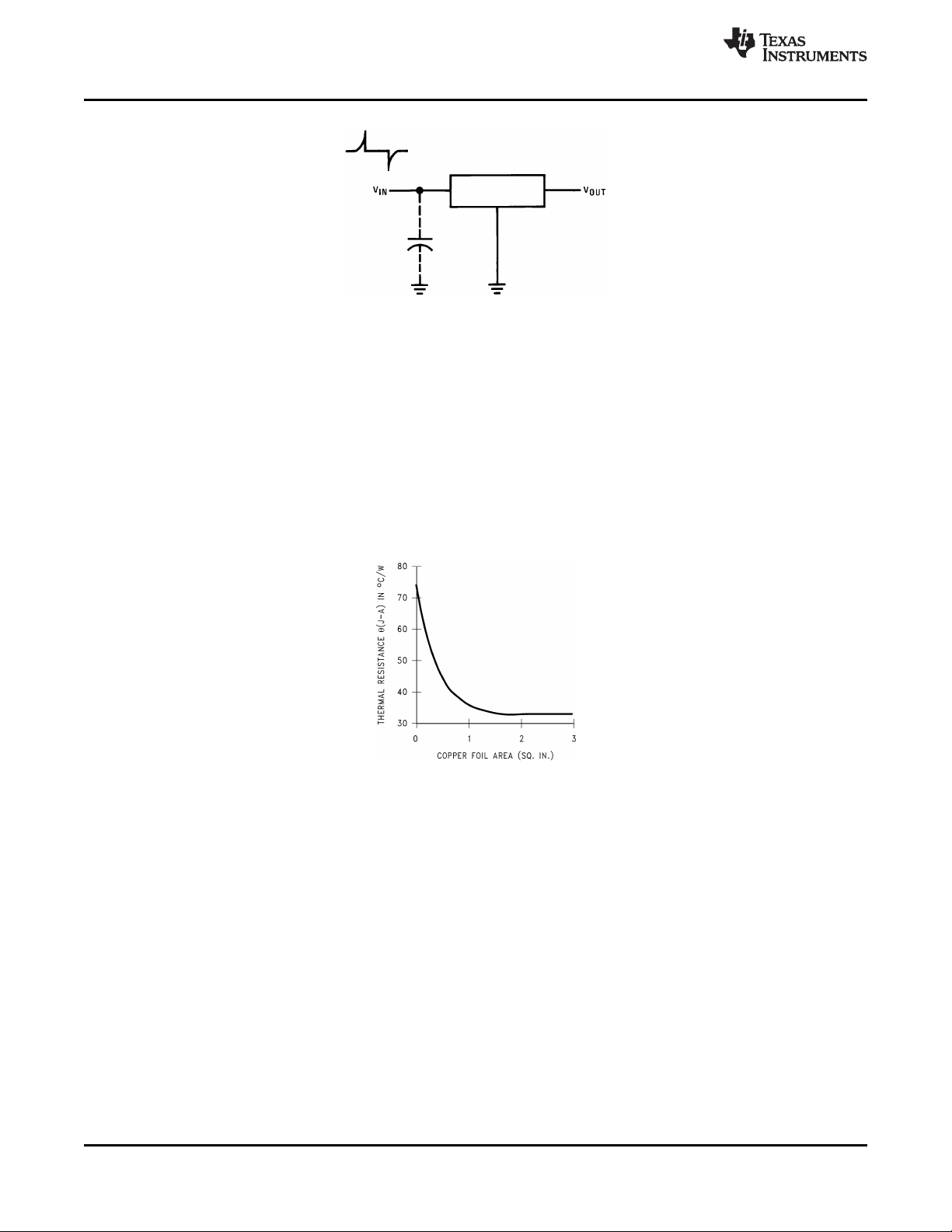
HEATSINKING DDPAK/TO-263 AND SOT-223 PACKAGE PARTS
Both the DDPAK/TO-263 (KTT) and SOT-223 (DCY) packages use a copper plane on the PCB and the PCB
itself as a heatsink. To optimize the heat sinking ability of the plane and PCB, solder the tab of the plane.
shows for the DDPAK/TO-263 the measured values of θ
with 1 ounce copper and no solder mask over the copper area used for heatsinking.
for different copper area sizes using a typical PCB
(J–A)
Figure 24. θ
vs Copper (1 ounce) Area for the DDPAK/TO-263 Package
(J–A)
As shown in the figure, increasing the copper area beyond 1 square inch produces very little improvement. It
should also be observed that the minimum value of θ
for the DDPAK/TO-263 package mounted to a PCB is
(J–A)
32°C/W.
As a design aid, Figure 25 shows the maximum allowable power dissipation compared to ambient temperature
for the DDPAK/TO-263 device (assuming θ
12 Submit Documentation Feedback Copyright © 2000–2013, Texas Instruments Incorporated
Product Folder Links: LM340-N LM78xx
is 35°C/W and the maximum junction temperature is 125°C).
(J–A)

LM340-N, LM78xx
www.ti.com
Figure 25. Maximum Power Dissipation vs T
AMB
SNOSBT0J –FEBRUARY 2000–REVISED DECEMBER 2013
for the DDPAK/TO-263 Package
Figure 26 and Figure 27 show the information for the SOT-223 package. Figure 26 assumes a θ
for 1 ounce copper and 51°C/W for 2 ounce copper and a maximum junction temperature of 125°C.
(J–A)
of 74°C/W
Figure 26. θ
vs Copper (2 ounce) Area
(J–A)
for the SOT-223 Package
Figure 27. Maximum Power Dissipation vs
T
for the SOT-223 Package
AMB
Please see AN-1028 (SNVA036) for power enhancement techniques to be used with the SOT-223 package.
Copyright © 2000–2013, Texas Instruments Incorporated Submit Documentation Feedback 13
Product Folder Links: LM340-N LM78xx

0.1 PF
0.22 PF
OUTPUTINPUT
GND
V
O
V
I
0.1 PF
(NOTE 1)
0.22 PF
OUTPUTINPUT
GND
V
O
V
I
0.1 PF0.22 PF
OUTPUTINPUT
GND
V
O
V
I
+
+
LM340-N, LM78xx
SNOSBT0J –FEBRUARY 2000–REVISED DECEMBER 2013
Typical Applications
Bypass capacitors are recommended for optimum stability and transient response, and should be located as close as
possible to the regulator.
Figure 28. Fixed Output Regulator
www.ti.com
Figure 29. High Input Voltage Circuits
14 Submit Documentation Feedback Copyright © 2000–2013, Texas Instruments Incorporated
Product Folder Links: LM340-N LM78xx

0.1 PF
0.22 PF
OUTPUT
INPUT
GND
OUT
R1
3.0:
Q1
2N6132
IN
R
SC
Q2
2N6124
0.1 PF
0.22 PF
OUTPUT
INPUT
GND
V
O
R1
3.0:
Q1
2N6133
IO MAX
I
Q1
I
REG
V
I
LM340-N, LM78xx
www.ti.com
SNOSBT0J –FEBRUARY 2000–REVISED DECEMBER 2013
Figure 30. High Current Voltage Regulator
Figure 31. High Output Current, Short Circuit Protected
Product Folder Links: LM340-N LM78xx
Copyright © 2000–2013, Texas Instruments Incorporated Submit Documentation Feedback 15

0.1 PF
OUTPUTINPUT
GND
+ OUT
+ +
0.1 PF
OUTPUTINPUT
GND
- OUT
+ +
LM340-N, LM78xx
SNOSBT0J –FEBRUARY 2000–REVISED DECEMBER 2013
Figure 32. Positive and Negative Regulator
www.ti.com
16 Submit Documentation Feedback Copyright © 2000–2013, Texas Instruments Incorporated
Product Folder Links: LM340-N LM78xx

LM340-N, LM78xx
www.ti.com
SNOSBT0J –FEBRUARY 2000–REVISED DECEMBER 2013
REVISION HISTORY
Changes from Revision I (March 2013) to Revision J Page
• Changed 0.5 from typ to max ............................................................................................................................................... 4
Copyright © 2000–2013, Texas Instruments Incorporated Submit Documentation Feedback 17
Product Folder Links: LM340-N LM78xx

PACKAGE OPTION ADDENDUM
www.ti.com
PACKAGING INFORMATION
Orderable Device Status
LM340AT-5.0 NRND TO-220 NDE 3 45 TBD Call TI Call TI 0 to 70 LM340AT
LM340AT-5.0/NOPB ACTIVE TO-220 NDE 3 45 Pb-Free (RoHS
LM340K-5.0 ACTIVE TO-3 NDS 2 50 TBD Call TI Call TI 0 to 70 LM340K
LM340K-5.0/NOPB ACTIVE TO-3 NDS 2 50 Green (RoHS
LM340MP-5.0 NRND SOT-223 DCY 4 1000 TBD Call TI Call TI 0 to 70 N00A
LM340MP-5.0/NOPB ACTIVE SOT-223 DCY 4 1000 Green (RoHS
LM340MPX-5.0/NOPB ACTIVE SOT-223 DCY 4 2000 Green (RoHS
LM340S-12/NOPB ACTIVE DDPAK/
LM340S-5.0 NRND DDPAK/
LM340S-5.0/NOPB ACTIVE DDPAK/
LM340SX-12/NOPB ACTIVE DDPAK/
LM340SX-5.0 NRND DDPAK/
LM340SX-5.0/NOPB ACTIVE DDPAK/
LM340T-12 NRND TO-220 NDE 3 45 TBD Call TI Call TI 0 to 70 LM340T12
LM340T-12/NOPB ACTIVE TO-220 NDE 3 45 Green (RoHS
LM340T-15 NRND TO-220 NDE 3 45 TBD Call TI Call TI 0 to 70 LM340T15
LM340T-15/NOPB ACTIVE TO-220 NDE 3 45 Green (RoHS
LM340T-5.0 NRND TO-220 NDE 3 45 TBD Call TI Call TI 0 to 70 LM340T5
Package Type Package
(1)
TO-263
TO-263
TO-263
TO-263
TO-263
TO-263
Drawing
Qty
KTT 3 45 Pb-Free (RoHS
KTT 3 45 TBD Call TI Call TI 0 to 70 LM340S
KTT 3 45 Pb-Free (RoHS
KTT 3 500 Pb-Free (RoHS
KTT 3 500 TBD Call TI Call TI 0 to 70 LM340S
KTT 3 500 Pb-Free (RoHS
Pins Package
Eco Plan
(2)
Exempt)
& no Sb/Br)
& no Sb/Br)
& no Sb/Br)
Exempt)
Exempt)
Exempt)
Exempt)
& no Sb/Br)
& no Sb/Br)
Lead/Ball Finish
(6)
MSL Peak Temp
(3)
Op Temp (°C) Device Marking
CU SN Level-1-NA-UNLIM 0 to 70 LM340AT
Call TI Level-1-NA-UNLIM 0 to 70 LM340K
CU SN Level-1-260C-UNLIM 0 to 70 N00A
CU SN Level-1-260C-UNLIM 0 to 70 N00A
CU SN Level-3-245C-168 HR 0 to 70 LM340S
CU SN Level-3-245C-168 HR 0 to 70 LM340S
CU SN Level-3-245C-168 HR 0 to 70 LM340S
CU SN Level-3-245C-168 HR 0 to 70 LM340S
CU SN Level-1-NA-UNLIM 0 to 70 LM340T12
CU SN Level-1-NA-UNLIM 0 to 70 LM340T15
11-Feb-2015
Samples
(4/5)
5.0 P+
5.0 P+
-5.0 7805P+
-5.0 7805P+
-12 P+
-5.0 P+
-5.0 P+
-12 P+
-5.0 P+
-5.0 P+
7812 P+
7812 P+
7815 P+
7815 P+
Addendum-Page 1

PACKAGE OPTION ADDENDUM
www.ti.com
Orderable Device Status
LM340T-5.0/LF01 ACTIVE TO-220 NDG 3 45 Pb-Free (RoHS
LM340T-5.0/NOPB ACTIVE TO-220 NDE 3 45 Pb-Free (RoHS
LM7812CT/NOPB ACTIVE TO-220 NDE 3 45 Green (RoHS
(1)
The marketing status values are defined as follows:
ACTIVE: Product device recommended for new designs.
LIFEBUY: TI has announced that the device will be discontinued, and a lifetime-buy period is in effect.
NRND: Not recommended for new designs. Device is in production to support existing customers, but TI does not recommend using this part in a new design.
PREVIEW: Device has been announced but is not in production. Samples may or may not be available.
OBSOLETE: TI has discontinued the production of the device.
Package Type Package
(1)
Drawing
Pins Package
Qty
Eco Plan
(2)
Exempt)
Exempt)
& no Sb/Br)
Lead/Ball Finish
(6)
CU SN Level-4-260C-72 HR LM340T5
CU SN Level-1-NA-UNLIM 0 to 70 LM340T5
CU SN Level-1-NA-UNLIM 0 to 70 LM340T12
MSL Peak Temp
(3)
Op Temp (°C) Device Marking
7805 P+
7805 P+
7805 P+
7812 P+
11-Feb-2015
(4/5)
(2)
Eco Plan - The planned eco-friendly classification: Pb-Free (RoHS), Pb-Free (RoHS Exempt), or Green (RoHS & no Sb/Br) - please check http://www.ti.com/productcontent for the latest availability
information and additional product content details.
TBD: The Pb-Free/Green conversion plan has not been defined.
Pb-Free (RoHS): TI's terms "Lead-Free" or "Pb-Free" mean semiconductor products that are compatible with the current RoHS requirements for all 6 substances, including the requirement that
lead not exceed 0.1% by weight in homogeneous materials. Where designed to be soldered at high temperatures, TI Pb-Free products are suitable for use in specified lead-free processes.
Pb-Free (RoHS Exempt): This component has a RoHS exemption for either 1) lead-based flip-chip solder bumps used between the die and package, or 2) lead-based die adhesive used between
the die and leadframe. The component is otherwise considered Pb-Free (RoHS compatible) as defined above.
Green (RoHS & no Sb/Br): TI defines "Green" to mean Pb-Free (RoHS compatible), and free of Bromine (Br) and Antimony (Sb) based flame retardants (Br or Sb do not exceed 0.1% by weight
in homogeneous material)
(3)
MSL, Peak Temp. - The Moisture Sensitivity Level rating according to the JEDEC industry standard classifications, and peak solder temperature.
(4)
There may be additional marking, which relates to the logo, the lot trace code information, or the environmental category on the device.
(5)
Multiple Device Markings will be inside parentheses. Only one Device Marking contained in parentheses and separated by a "~" will appear on a device. If a line is indented then it is a continuation
of the previous line and the two combined represent the entire Device Marking for that device.
(6)
Lead/Ball Finish - Orderable Devices may have multiple material finish options. Finish options are separated by a vertical ruled line. Lead/Ball Finish values may wrap to two lines if the finish
value exceeds the maximum column width.
Important Information and Disclaimer:The information provided on this page represents TI's knowledge and belief as of the date that it is provided. TI bases its knowledge and belief on information
provided by third parties, and makes no representation or warranty as to the accuracy of such information. Efforts are underway to better integrate information from third parties. TI has taken and
Samples
Addendum-Page 2
PACKAGE OPTION ADDENDUM
www.ti.com
continues to take reasonable steps to provide representative and accurate information but may not have conducted destructive testing or chemical analysis on incoming materials and chemicals.
TI and TI suppliers consider certain information to be proprietary, and thus CAS numbers and other limited information may not be available for release.
11-Feb-2015
In no event shall TI's liability arising out of such information exceed the total purchase price of the TI part(s) at issue in this document sold by TI to Customer on an annual basis.
Addendum-Page 3

PACKAGE MATERIALS INFORMATION
www.ti.com 5-Dec-2014
TAPE AND REEL INFORMATION
*All dimensions are nominal
Device Package
LM340MP-5.0 SOT-223 DCY 4 1000 330.0 16.4 7.0 7.5 2.2 12.0 16.0 Q3
LM340MP-5.0/NOPB SOT-223 DCY 4 1000 330.0 16.4 7.0 7.5 2.2 12.0 16.0 Q3
LM340MPX-5.0/NOPB SOT-223 DCY 4 2000 330.0 16.4 7.0 7.5 2.2 12.0 16.0 Q3
LM340SX-12/NOPB DDPAK/
TO-263
LM340SX-5.0 DDPAK/
TO-263
LM340SX-5.0/NOPB DDPAK/
TO-263
Type
Package
Drawing
Pins SPQ Reel
Diameter
(mm)
KTT 3 500 330.0 24.4 10.75 14.85 5.0 16.0 24.0 Q2
KTT 3 500 330.0 24.4 10.75 14.85 5.0 16.0 24.0 Q2
KTT 3 500 330.0 24.4 10.75 14.85 5.0 16.0 24.0 Q2
Reel
Width
W1 (mm)
A0
(mm)B0(mm)K0(mm)P1(mm)W(mm)
Pin1
Quadrant
Pack Materials-Page 1

PACKAGE MATERIALS INFORMATION
www.ti.com 5-Dec-2014
*All dimensions are nominal
Device Package Type Package Drawing Pins SPQ Length (mm) Width (mm) Height (mm)
LM340MP-5.0 SOT-223 DCY 4 1000 367.0 367.0 35.0
LM340MP-5.0/NOPB SOT-223 DCY 4 1000 367.0 367.0 35.0
LM340MPX-5.0/NOPB SOT-223 DCY 4 2000 367.0 367.0 35.0
LM340SX-12/NOPB DDPAK/TO-263 KTT 3 500 367.0 367.0 45.0
LM340SX-5.0 DDPAK/TO-263 KTT 3 500 367.0 367.0 45.0
LM340SX-5.0/NOPB DDPAK/TO-263 KTT 3 500 367.0 367.0 45.0
Pack Materials-Page 2

NDS0002A
MECHANICAL DATA
www.ti.com

NDE0003B
MECHANICAL DATA
www.ti.com

NDG0003F
MECHANICAL DATA
www.ti.com
T03F (Rev B)

MECHANICAL DATA
MPDS094A – APRIL 2001 – REVISED JUNE 2002
DCY (R-PDSO-G4) PLASTIC SMALL-OUTLINE
6,70 (0.264)
6,30 (0.248)
3,10 (0.122)
4
2,90 (0.114)
0,10 (0.004)
M
7,30 (0.287)
6,70 (0.264)
1 2 3
2,30 (0.091)
4,60 (0.181)
1,80 (0.071) MAX
0,10 (0.0040)
0,02 (0.0008)
NOTES: A. All linear dimensions are in millimeters (inches).
B. This drawing is subject to change without notice.
C. Body dimensions do not include mold flash or protrusion.
D. Falls within JEDEC TO-261 Variation AA.
3,70 (0.146)
3,30 (0.130)
0,84 (0.033)
0,66 (0.026)
0,10 (0.004)
1,70 (0.067)
1,50 (0.059)
Seating Plane
M
0,08 (0.003)
0°–10°
Gauge Plane
0,25 (0.010)
0,75 (0.030) MIN
0,35 (0.014)
0,23 (0.009)
4202506/B 06/2002
POST OFFICE BOX 655303 • DALLAS, TEXAS 75265

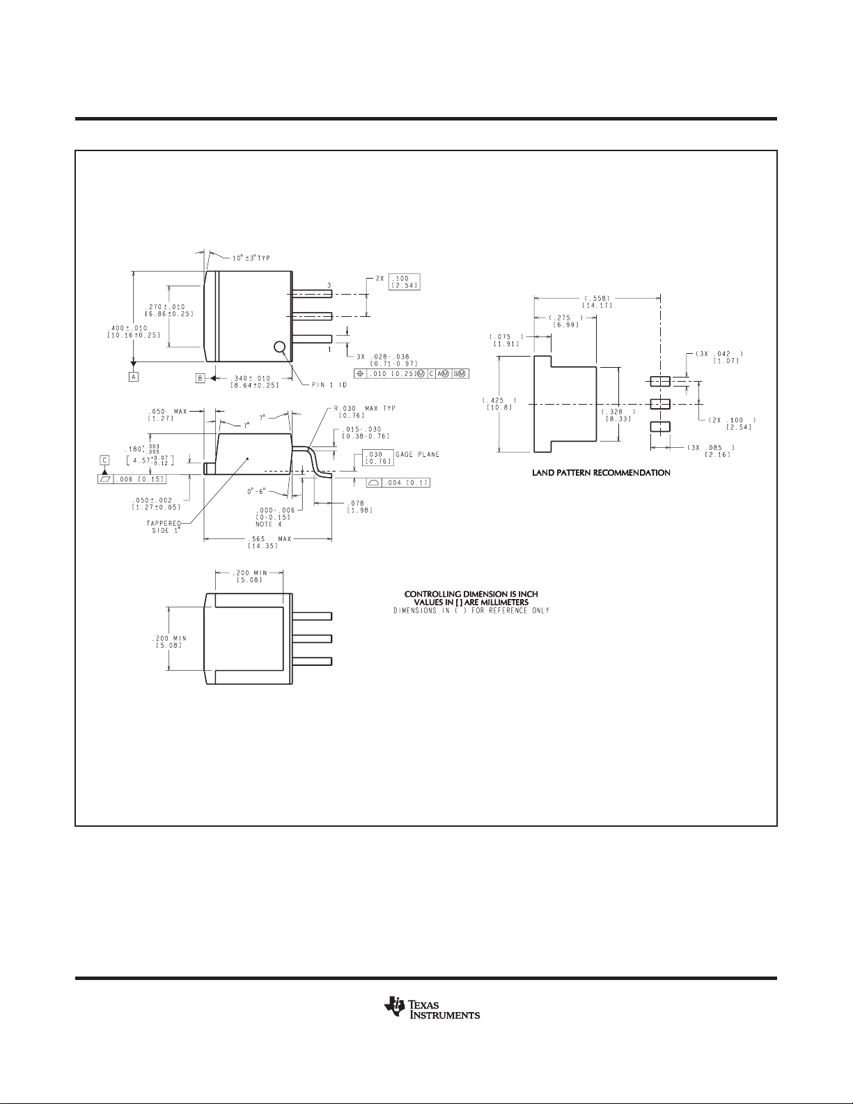
KTT0003B
MECHANICAL DATA
BOTTOM SIDE OF PACKAGE
TS3B (Rev F)
www.ti.com

IMPORTANT NOTICE
Texas Instruments Incorporated and its subsidiaries (TI) reserve the right to make corrections, enhancements, improvements and other
changes to its semiconductor products and services per JESD46, latest issue, and to discontinue any product or service per JESD48, latest
issue. Buyers should obtain the latest relevant information before placing orders and should verify that such information is current and
complete. All semiconductor products (also referred to herein as “components”) are sold subject to TI’s terms and conditions of sale
supplied at the time of order acknowledgment.
TI warrants performance of its components to the specifications applicable at the time of sale, in accordance with the warranty in TI’s terms
and conditions of sale of semiconductor products. Testing and other quality control techniques are used to the extent TI deems necessary
to support this warranty. Except where mandated by applicable law, testing of all parameters of each component is not necessarily
performed.
TI assumes no liability for applications assistance or the design of Buyers’ products. Buyers are responsible for their products and
applications using TI components. To minimize the risks associated with Buyers’ products and applications, Buyers should provide
adequate design and operating safeguards.
TI does not warrant or represent that any license, either express or implied, is granted under any patent right, copyright, mask work right, or
other intellectual property right relating to any combination, machine, or process in which TI components or services are used. Information
published by TI regarding third-party products or services does not constitute a license to use such products or services or a warranty or
endorsement thereof. Use of such information may require a license from a third party under the patents or other intellectual property of the
third party, or a license from TI under the patents or other intellectual property of TI.
Reproduction of significant portions of TI information in TI data books or data sheets is permissible only if reproduction is without alteration
and is accompanied by all associated warranties, conditions, limitations, and notices. TI is not responsible or liable for such altered
documentation. Information of third parties may be subject to additional restrictions.
Resale of TI components or services with statements different from or beyond the parameters stated by TI for that component or service
voids all express and any implied warranties for the associated TI component or service and is an unfair and deceptive business practice.
TI is not responsible or liable for any such statements.
Buyer acknowledges and agrees that it is solely responsible for compliance with all legal, regulatory and safety-related requirements
concerning its products, and any use of TI components in its applications, notwithstanding any applications-related information or support
that may be provided by TI. Buyer represents and agrees that it has all the necessary expertise to create and implement safeguards which
anticipate dangerous consequences of failures, monitor failures and their consequences, lessen the likelihood of failures that might cause
harm and take appropriate remedial actions. Buyer will fully indemnify TI and its representatives against any damages arising out of the use
of any TI components in safety-critical applications.
In some cases, TI components may be promoted specifically to facilitate safety-related applications. With such components, TI’s goal is to
help enable customers to design and create their own end-product solutions that meet applicable functional safety standards and
requirements. Nonetheless, such components are subject to these terms.
No TI components are authorized for use in FDA Class III (or similar life-critical medical equipment) unless authorized officers of the parties
have executed a special agreement specifically governing such use.
Only those TI components which TI has specifically designated as military grade or “enhanced plastic” are designed and intended for use in
military/aerospace applications or environments. Buyer acknowledges and agrees that any military or aerospace use of TI components
which have not been so designated is solely at the Buyer's risk, and that Buyer is solely responsible for compliance with all legal and
regulatory requirements in connection with such use.
TI has specifically designated certain components as meeting ISO/TS16949 requirements, mainly for automotive use. In any case of use of
non-designated products, TI will not be responsible for any failure to meet ISO/TS16949.
Products Applications
Audio www.ti.com/audio Automotive and Transportation www.ti.com/automotive
Amplifiers amplifier.ti.com Communications and Telecom www.ti.com/communications
Data Converters dataconverter.ti.com Computers and Peripherals www.ti.com/computers
DLP® Products www.dlp.com Consumer Electronics www.ti.com/consumer-apps
DSP dsp.ti.com Energy and Lighting www.ti.com/energy
Clocks and Timers www.ti.com/clocks Industrial www.ti.com/industrial
Interface interface.ti.com Medical www.ti.com/medical
Logic logic.ti.com Security www.ti.com/security
Power Mgmt power.ti.com Space, Avionics and Defense www.ti.com/space-avionics-defense
Microcontrollers microcontroller.ti.com Video and Imaging www.ti.com/video
RFID www.ti-rfid.com
OMAP Applications Processors www.ti.com/omap TI E2E Community e2e.ti.com
Wireless Connectivity www.ti.com/wirelessconnectivity
Mailing Address: Texas Instruments, Post Office Box 655303, Dallas, Texas 75265
Copyright © 2015, Texas Instruments Incorporated

 Loading...