

Features
■ Inductor switches boost controller
■ PFM mode control
■ High efficiency over wide range of load (1 mA
to 40 mA)
■ Integrated load disconnect switch
■ Over voltage protection with automatic restart
■ Soft start with adjustable peak current limit
■ Enable pin
■ Low shutdown current
■ Small external inductor
■ Supply voltage from 3.0 V to 5.5 V
Application
■ PMOLED display driver
Description
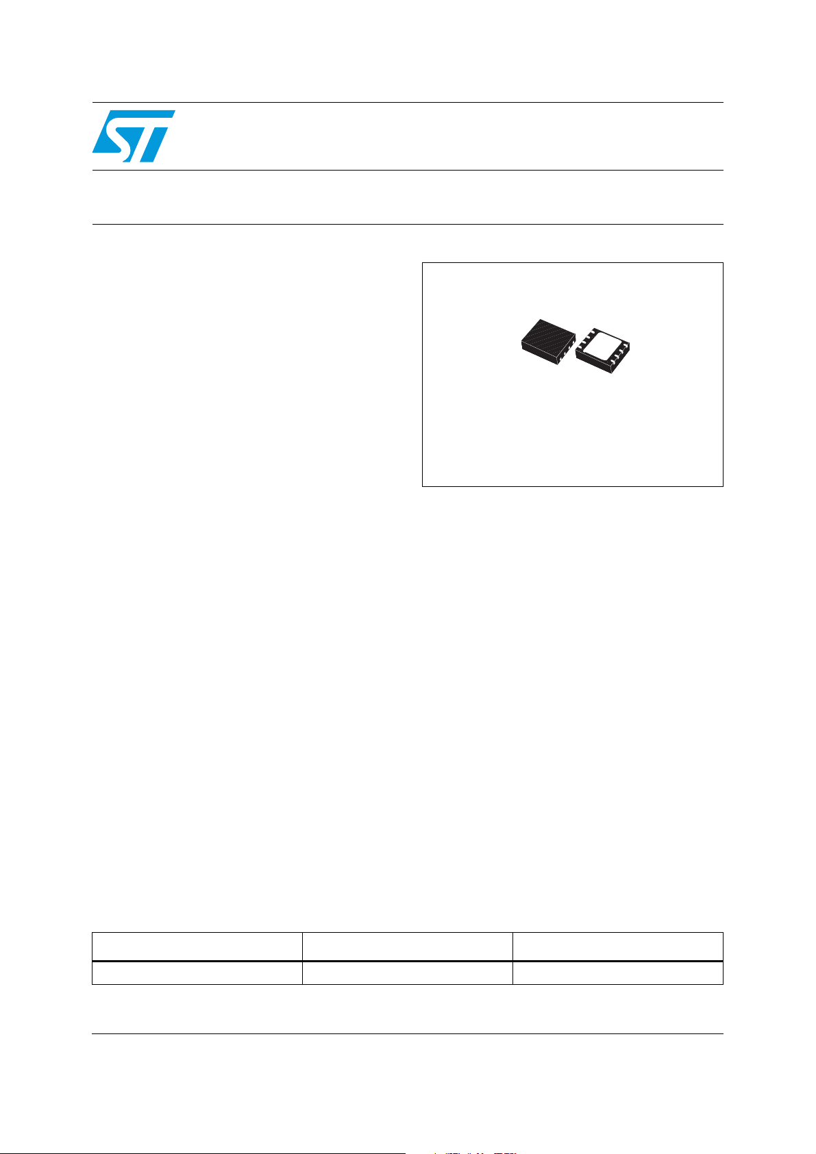
STOD2540
PMOLED display power supply
QFN8 (3 x 3 mm)
In this state-of-the-art boost converter, a DC
current path exists between the battery source
and the load. In order to reduce the consumption
in shutdown mode, a high-side load isolation
switch is necessary to cut this DC current path in
standby mode. The load disconnect switch (LDS)
act as an isolation switch in shutdown mode.
STOD2540 is dedicated to passive matrix OLED
(PMOLED) displays for portable handsets and
provides the pre-charge and biasing voltage of
the column matrix driver as shown in figure 3. The
current capability of STOD2540 allows feeding a
1", 1.3" or 1.5" color PMOLED. STOD2540 is a
boost converter that operates from 3.0 V to 5.5 V
and can provide an output voltage as high as 25
V. The output current capability is maximum 40
mA up to 25 V output voltage. The regulation is
performed by a resistor divider network (figure 3)
that detects the output voltage.
Table 1. Device summary
Order code Package Packaging
STOD2540PUR QFN8 (3 x 3 mm) 3000 parts per reel
July 2010 Doc ID 12204 Rev 10 1/20
www.st.com
20

Contents STOD2540
Contents
1 Diagram . . . . . . . . . . . . . . . . . . . . . . . . . . . . . . . . . . . . . . . . . . . . . . . . . . . 3
2 Pin configuration . . . . . . . . . . . . . . . . . . . . . . . . . . . . . . . . . . . . . . . . . . . . 4
3 Maximum ratings . . . . . . . . . . . . . . . . . . . . . . . . . . . . . . . . . . . . . . . . . . . . 5
4 Electrical characteristics . . . . . . . . . . . . . . . . . . . . . . . . . . . . . . . . . . . . . 6
5 Functional description . . . . . . . . . . . . . . . . . . . . . . . . . . . . . . . . . . . . . . . 8
5.1 Boost controller . . . . . . . . . . . . . . . . . . . . . . . . . . . . . . . . . . . . . . . . . . . . . 8
5.2 Adjustable peak inductor current limit . . . . . . . . . . . . . . . . . . . . . . . . . . . . 8
5.3 Enable . . . . . . . . . . . . . . . . . . . . . . . . . . . . . . . . . . . . . . . . . . . . . . . . . . . . 8
5.4 OVP . . . . . . . . . . . . . . . . . . . . . . . . . . . . . . . . . . . . . . . . . . . . . . . . . . . . . . 8
5.5 Load isolation switch . . . . . . . . . . . . . . . . . . . . . . . . . . . . . . . . . . . . . . . . . 9
5.6 Efficiency . . . . . . . . . . . . . . . . . . . . . . . . . . . . . . . . . . . . . . . . . . . . . . . . . . 9
5.7 Under voltage lockout (UVLO) . . . . . . . . . . . . . . . . . . . . . . . . . . . . . . . . . . 9
6 Typical application . . . . . . . . . . . . . . . . . . . . . . . . . . . . . . . . . . . . . . . . . 10
6.1 Demonstration board . . . . . . . . . . . . . . . . . . . . . . . . . . . . . . . . . . . . . . . . 11
7 Typical performance characteristics . . . . . . . . . . . . . . . . . . . . . . . . . . . 12
8 Package mechanical data . . . . . . . . . . . . . . . . . . . . . . . . . . . . . . . . . . . . 15
9 Revision history . . . . . . . . . . . . . . . . . . . . . . . . . . . . . . . . . . . . . . . . . . . 19
2/20 Doc ID 12204 Rev 10

STOD2540 Diagram
1 Diagram
Figure 1. Block diagram
Doc ID 12204 Rev 10 3/20

Pin configuration STOD2540
2 Pin configuration
Figure 2. Pin connections (top through view)
Table 2. Pin description
Pin n° Symbol Note
1V
2R
SET
Supply voltage
I
Peak inductor current adjust
3 AGND Analog ground
4 FB Feedback for the LED current regulation
5V
6V
O
CAP
Output voltage for LED supply
Load disconnect switch input
7 EN IC enable signal
8V
SW
Boost switch drain
PGND Power ground
4/20 Doc ID 12204 Rev 10
STOD2540 Maximum ratings
3 Maximum ratings
Table 3. Absolute maximum ratings
Symbol Parameter Value Unit
VB
SW, VBO
V
I
R
SET
EN Enable pin V
V
ESD
T
STG
T
OP
Breakdown voltage at OUT and SW pin 40 V
Supply voltage range 6 V
R
pin VI + 0.3 V
SET
+ 0.3 V
I
ESD ratings, HBM MIL STD 883C 2 kV
Storage temperature range - 65 to 150 °C
Operating junction temperature range - 40 to 85 °C
Table 4. Thermal data
Symbol Parameter Value Unit
R
thJA
Thermal resistance junction-ambient 52 °C/W
Doc ID 12204 Rev 10 5/20

Electrical characteristics STOD2540
4 Electrical characteristics
TJ = 40 °C to 85 °C, VI = 3.6 V, VEN = 3V, CI = CO = 4.7 µF, L = 4.7 µH, R1 = 180 kΩ,
R
= 10 kΩ, VO = 24 V, Typ. values @ 25 °C, unless otherwise specified.
2
Table 5. Electrical characteristics
Symbol Parameter Test condition Min. Typ. Max. Unit
V
V
V
OVP
I
I
SD
I
R
DSON-SW
O
O
Q
Input voltage range 3.0 5.5 V
I
= 3 V to 5.5 V VI + 0.5
Regulated output voltage
Over voltage protection on
output
Continuous output current
Stand-by current
Quiescent current consumption
Boost switch R
DSON
(1)
V
I
= 25 V
V
O
V
= Low, VI = 3.6 V
EN
V
= Low, VI = 3 V to 4.2 V
EN
V
= 3 V to 4.2 V @ 25 °C
I
= 5.5 V @ 25 °C
V
I
VI = 4.2 V, ISW = 100 mA
35 V
140mA
25 35 V
0.4 0.8
0.8 1.2
0.4 Ω
BVDS Breakdown voltage 40 V
R
DSON-
LDS
R
DSON
(1)
VO = 25 V, IO = 30 mA
2 Ω
BVDS Breakdown voltage 40 V
I
LIM-ADJ
I
LIM-MAX
Peak inductor limit range
Maximum peak inductor current
(1)
(1)
R
= 10 kΩ to 100 kΩ
SET
VI = 3 V to 5.5 V, R
SET
= V
0.2 1.1 A
I
0.75 1.2 A
FB Feedback voltage 5% @ 25 °C 1.18 1.24 1.30 V
T
ON_MAX
T
OFF_MIN
Maximum ON time
Minimum OFF time
Efficiency, V
= 3.6 V
I
Eff
Efficiency, V
= 4.2 V
I
Ripple Output ripple and noise
OV
HYST
Over-voltage hysteresis 2 V
(1)
(1)
= 4.2 V
V
I
= 4.2 V
V
I
IO = 1 mA to 5 mA
= 5 mA to 40 mA
I
O
IO = 1 mA to 5 mA
I
= 5 mA to 40 mA
O
V
= 3.6 V, IO = 5 mA, VO = 24 V
I
V
= 3.6 V, IO = 30 mA, VO = 24 V
I
V
= 4.2 V, IO = 5 mA, VO = 24 V
I
= 4.2 V, IO = 30 mA, VO = 24 V
V
I
5.5 µs
300 ns
65
70
65
70
1.3
1.3
1.3
1.3
3
µA
10
mA
%
%
6/20 Doc ID 12204 Rev 10

STOD2540 Electrical characteristics
Table 5. Electrical characteristics (continued)
Symbol Parameter Test condition Min. Typ. Max. Unit
V
Enable input logic low
EN
Line_V
Load_V
1. Guaranteed by design.
Enable input logic high
Line regulation V
FB
Line regulation V
FB
FB
FB
Disable Low V
Enable High V
IL
IH
1.2
0.3
V
VI = 3 V to 5.5 V, IO = 5 mA 5 35 mV
VI = 3 V to 5.5 V, IO = 5 mA 5 35 mV
Doc ID 12204 Rev 10 7/20

Functional description STOD2540
5 Functional description
5.1 Boost controller
STOD2540 is a boost converter operating in PFM (pulsed frequency modulation) mode. The
converter monitors the output voltage through the bridge resistor divider R
when the feedback voltage falls below the reference voltage, REF2, the boost switch t
turns ON and the current ramps up. The inductor current is measured by detect the
temperature compensated drain voltage of the boost MOSFET. The boost turns off when its
drain voltage reaches the reference REF1, the main switch remains off until the minimum off
time (300 ns typical) has passed and the feedback voltage is below the reference again. A
maximum ON time of 4 µs prevent the switch t
to stay ON during a too long period of
SW
time.
and R2 and
1
SW
In order to well calculate the bridge resistors values with a fixed V
can be used:
(V
/ 1.24) -1 = R1 / R
O
2
5.2 Adjustable peak inductor current limit
The peak inductor current is monitored by sensing the drain voltage of the switch tSW.
Since it exceeds the temperature compensated and supply voltage compensated reference
REF1, the RS flip flop is reset and t
By connecting a resistance between the pin R
adjusted from 200 mA to 1.1 A (R
connected to V
, the default value is 1 A.
I
is turned OFF.
SW
and GND, the peak current limit can be
from 10 kΩ to 100 kΩ). When the pin R
SET
SET
5.3 Enable
The ENABLE pin is a high logic input signal and allows turning on/off the controller without
cutting the input voltage from the boost regulator circuit. With a high input voltage (1.2 V <
V
< VI + 0.3 V) on this pin, the device is allowed to work normally. No pull-up or pull down
EN
is present on this pin.
, the following formula
O
is directly
SET
5.4 OVP
If the regulation loop is cut, there is no signal at the feedback pin, the PFM controller will
then continue to switch without control and generate an output voltage at the SW, V
V
pin exceeding the breakdown value V
O
The over voltage protection (OVP) senses the voltage at the V
exceed the breakdown voltage of the device the controller is automatically turned off.
A hysteresis control enables the device to automatically restart when the output voltage
drops below a 2 V typical value.
8/20 Doc ID 12204 Rev 10
BSW
, V
BCAP
and VBO.
pin. When the voltage
CAP
CAP
and

STOD2540 Functional description
5.5 Load isolation switch
When the device is in shutdown mode, a DC current path always exists between the power
source and the load; increasing the standby consumption. A high side switch LDS isolates
the load from the source when the STOD2540 is disabled.
5.6 Efficiency
The total consumption of some PMOLED display, can be as low as 1 mA. In order to
increase the battery run time of the device, STOD2540 offers a high efficiency over a wide
range of load and input voltage range.
5.7 Under voltage lockout (UVLO)
The minimum supply voltage is 3.0 V, under this value the under voltage lockout circuit
operates with typical threshold 2.8 V.
When supply voltage is below 3.0 V, possible noise in the supply line could disturb the UVLO
circuit causing loss of output regulation. This behavior is eliminated choosing C
higher.
= 10 µF or
I
Doc ID 12204 Rev 10 9/20

Typical application STOD2540
6 Typical application
Figure 3. Basic connection
Table 6. External components (see Figure 3)
Symbol Parameter Test Min. Typ. Max. Unit
VRRM 30 V
D Boost schottky diode
R
R
SET
C
Feedback resistor 180
1
Feedback resistor 10
2
Peak current limit adjust IPK = 200 mA to 1.1 A 10 100
Input ceramic type low ESR Ceramic type 4.7 µF
I
VF at IF = 300 mA, TJ = 25 °C 0.5 V
at VR = 10 V, TJ = 25 °C 30 µA
I
R
kΩR
Capacitance 4.7 µF
C
O
Output capacitance: ceramic
low ESR
Voltage 42 V
ESR 1.6 W
Inductance 4.7 µH
L Boost inductor (height < 2mm)
I
, R
SAT
SET
pin to V
I
1A
Note: The external components suggested in this document should be considered as a design
reference guide. The performances mentioned in the electrical characteristics table are not
guaranteed for all the possible electrical parameters of the components included in this list.
On other hand, the operation of STOD2540 is not limited to the use of components included
in this list.
10/20 Doc ID 12204 Rev 10

STOD2540 Typical application
6.1 Demonstration board
Figure 4. Suggested demonstration board schematic (top layer view)
Doc ID 12204 Rev 10 11/20

Typical performance characteristics STOD2540
7 Typical performance characteristics
TJ = 40 °C to 85 °C, VI = 3.6 V, VEN = 3 V, CI = CO = 4.7 µF, L = 4.7 µH, R1 = 180 kΩ,
R
= 10 kΩ, VO = 24 V, Typ. values @ 25 °C, unless otherwise specified.
2
Figure 5. Efficiency vs. output current Figure 6. Efficiency vs. input voltage
Figure 7. VEN vs. temperature Figure 8. VFB vs. input voltage
Figure 9. VFB vs. output current Figure 10. VFB vs. output current
12/20 Doc ID 12204 Rev 10

STOD2540 Typical performance characteristics
Figure 11. V
Figure 13. I
vs. temperature Figure 12. V
OVP
LIM_MAX
vs. input voltage Figure 14. I
RIPPLE
LIM_MAX
vs. input voltage
vs. temperature
Figure 15. I
LIM_MAX
vs. R
SET
Doc ID 12204 Rev 10 13/20
Figure 16. IQ vs. temperature

Typical performance characteristics STOD2540
Figure 17. t
Figure 19. Line VFB vs. temperature Figure 20. Load VFB vs. temperature
ON_MAX
vs. temperature Figure 18. t
OFF_MIN
vs. temperature
14/20 Doc ID 12204 Rev 10

STOD2540 Package mechanical data
8 Package mechanical data
In order to meet environmental requirements, ST offers these devices in different grades of
ECOPACK
specifications, grade definitions and product status are available at: www.st.com.
ECOPACK
®
packages, depending on their level of environmental compliance. ECOPACK®
®
is an ST trademark.
Table 7. QFN8 (3 x 3 mm) mechanical data
Dim.
Min. Typ. Max.
A 0.800.901.00
A1 0 0.02 0.05
A3 0.20
b 0.250.300.35
mm.
D 2.853.003.15
D2 2.49 2.64 2.74
E 2.853.003.15
E2 1.75 1.90 2.00
e0.65
L 0.300.400.50
Doc ID 12204 Rev 10 15/20

Package mechanical data STOD2540
Figure 21. Drawing dimension QFN8 (3 x 3 mm)
16/20 Doc ID 12204 Rev 10
8057023_B

STOD2540 Package mechanical data
Tape & reel QFNxx/DFNxx (3x3) mechanical data
mm. inch.
Dim.
Min. Typ. Max. Min. Typ. Max.
A180 7.087
C 12.8 13.2 0.504 0.519
D 20.2 0.795
N60 2.362
T 14.4 0.567
Ao 3.3 0.130
Bo 3.3 0.130
Ko 1.1 0.043
Po 4 0.157
P 8 0.315
Doc ID 12204 Rev 10 17/20

Package mechanical data STOD2540
Figure 22. QFN8 (3x3) footprint recommended data
18/20 Doc ID 12204 Rev 10

STOD2540 Revision history
9 Revision history
Table 8. Document revision history
Date Revision Changes
22-Mar-2006 1 Initial release.
03-Apr-2006 2 Add fig. 2 demonstration board on page 3.
08-Jun-2006 3 Description in cover page updated.
23-Jun-2006 4 Change range of R
11-Sep-2006 5 Mistake on table 4 Ripple test value 3.6 V ==> 4.2 V.
27-Feb-2009 6 Modified mechanical data.
03-Mar-2009 7 Modified packaging Table1 on page1.
11-Mar-2009 8 Modified Figure 2 on page 4 and added Figure 22 on page 18.
25-Nov-2009 9 Modified Table 1 on page 1.
01-Jul-2010 10 Modified: Table 7 on page 15, Figure 21 on page 16 and Figure 22 on page 18.
value and add description paragraph 5.7.
SET
Doc ID 12204 Rev 10 19/20

STOD2540
Please Read Carefully:
Information in this document is provided solely in connection with ST products. STMicroelectronics NV and its subsidiaries (“ST”) reserve the
right to make changes, corrections, modifications or improvements, to this document, and the products and services described herein at any
time, without notice.
All ST products are sold pursuant to ST’s terms and conditions of sale.
Purchasers are solely responsible for the choice, selection and use of the ST products and services described herein, and ST assumes no
liability whatsoever relating to the choice, selection or use of the ST products and services described herein.
No license, express or implied, by estoppel or otherwise, to any intellectual property rights is granted under this document. If any part of this
document refers to any third party products or services it shall not be deemed a license grant by ST for the use of such third party products
or services, or any intellectual property contained therein or considered as a warranty covering the use in any manner whatsoever of such
third party products or services or any intellectual property contained therein.
UNLESS OTHERWISE SET FORTH IN ST’S TERMS AND CONDITIONS OF SALE ST DISCLAIMS ANY EXPRESS OR IMPLIED
WARRANTY WITH RESPECT TO THE USE AND/OR SALE OF ST PRODUCTS INCLUDING WITHOUT LIMITATION IMPLIED
WARRANTIES OF MERCHANTABILITY, FITNESS FOR A PARTICULAR PURPOSE (AND THEIR EQUIVALENTS UNDER THE LAWS
OF ANY JURISDICTION), OR INFRINGEMENT OF ANY PATENT, COPYRIGHT OR OTHER INTELLECTUAL PROPERTY RIGHT.
UNLESS EXPRESSLY APPROVED IN WRITING BY AN AUTHORIZED ST REPRESENTATIVE, ST PRODUCTS ARE NOT
RECOMMENDED, AUTHORIZED OR WARRANTED FOR USE IN MILITARY, AIR CRAFT, SPACE, LIFE SAVING, OR LIFE SUSTAINING
APPLICATIONS, NOR IN PRODUCTS OR SYSTEMS WHERE FAILURE OR MALFUNCTION MAY RESULT IN PERSONAL INJURY,
DEATH, OR SEVERE PROPERTY OR ENVIRONMENTAL DAMAGE. ST PRODUCTS WHICH ARE NOT SPECIFIED AS "AUTOMOTIVE
GRADE" MAY ONLY BE USED IN AUTOMOTIVE APPLICATIONS AT USER’S OWN RISK.
Resale of ST products with provisions different from the statements and/or technical features set forth in this document shall immediately void
any warranty granted by ST for the ST product or service described herein and shall not create or extend in any manner whatsoever, any
liability of ST.
ST and the ST logo are trademarks or registered trademarks of ST in various countries.
Information in this document supersedes and replaces all information previously supplied.
The ST logo is a registered trademark of STMicroelectronics. All other names are the property of their respective owners.
© 2010 STMicroelectronics - All rights reserved
STMicroelectronics group of companies
Australia - Belgium - Brazil - Canada - China - Czech Republic - Finland - France - Germany - Hong Kong - India - Israel - Italy - Japan -
Malaysia - Malta - Morocco - Philippines - Singapore - Spain - Sweden - Switzerland - United Kingdom - United States of America
www.st.com
20/20 Doc ID 12204 Rev 10
 Loading...