Sony STR-DH130 Service Manual
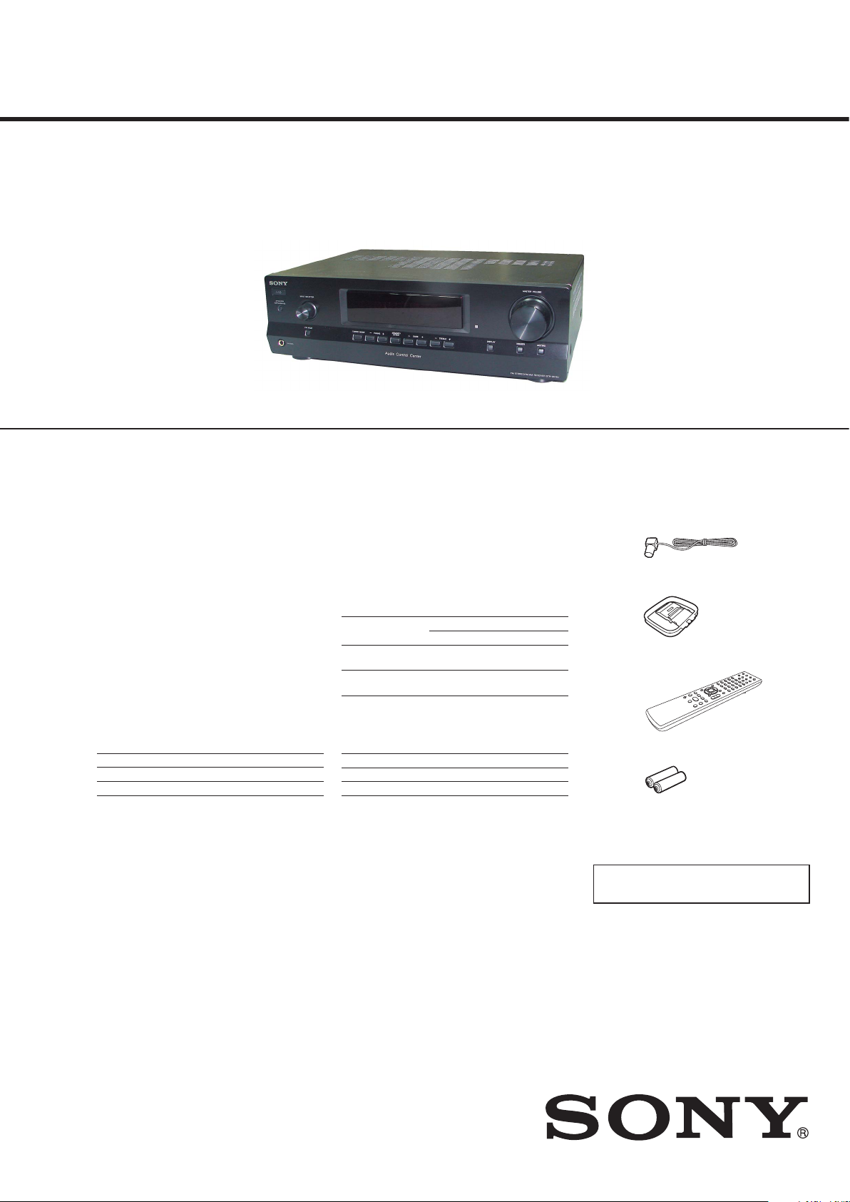
STR-DH130
SERVICE MANUAL
Ver. 1.0 2012.01
Specifi cations
AUDIO POWER
SPECIFICATIONS
POWER OUTPUT AND TOTAL
HARMONIC DISTORTION:
(US model only)
With 8 ohm loads, both channels driven, from
20 – 20,000 Hz; rated 90 watts per channel
minimum RMS power, with no more than 0.09%
total harmonic distortion from 250 milliwatts to
rated output.
Amplifi er section
US, Canadian and AEP models
Minimum RMS Output Power (8 ohms, 20 Hz –
20 kHz, THD 0.09%)
90 W + 90 W
Stereo Mode Output Power (8 ohms, 1 kHz,
THD 1%)
100 W + 100 W
1)
Measured under the following conditions:
Area Power requirements
US, Canadian 120 V AC, 60 Hz
AEP 230 V AC, 50 Hz
Frequency response
Analog 10 Hz – 70 kHz
+0.5/–2 dB (with BASS =
0 dB, TREBLE = 0 dB)
Input
Analog (PORTABLE IN)
Sensitivity: 1 V/
50 kilohms
S/N
Inputs
Analog (Except PORTABLE IN)
Sensitivity: 500 mV/
50 kilohms
S/N
Outputs
Analog (AUDIO OUT)
Voltage: 500 mV/
10 kilohms
1)
2)
: 96 dB (A, 500 mV3))
2)
: 96 dB (A, 500 mV3))
Tone
Gain levels ±10 dB, 1 dB step
2)
INPUT SHORT (with BASS = 0 dB, TREBLE =
0 dB).
3)
Weighted network, input level.
FM tuner section
Tuning range 87.5 MHz – 108.0 MHz
Antenna (aerial) FM wire antenna (aerial)
Antenna (aerial) terminals
75 ohms, unbalanced
AM tuner section
Tuning range
Area Tuning scale
US, Canadian 530 kHz – 531 kHz –
AEP
Antenna (aerial) Loop antenna (aerial)
General
Power requirements
Area Power requirements
US, Canadian 120 V AC, 60 Hz
AEP 230 V AC, 50/60 Hz
Power consumption 200 W
Power consumption (during standby mode)
0.3 W
Dimensions (w/h/d) (Approx.)
430 mm × 132.5 mm ×
279 mm (17 in × 5 1/4 in ×
11 in) including projecting
parts and controls
Mass (Approx.) 6.4 kg (14 lb 2 oz)
10 kHz step 9 kHz step
1,710 kHz 1,710 kHz
– 531 kHz –
1,602 kHz
US Model
Canadian Model
AEP Model
Supplied accessories
s Operating Instructions
s Quick Setup Guide
s FM wire antenna (aerial) (1)
s AM loop antenna (aerial) (1)
s Remote control (RM-AAU130) (1)
s R6 (size AA) batteries (2)
Design and specifi cations are subject to
change without notice.
Halogenated fl ame retardants are not used in
the certain printed wiring boards.
9-890-596-01
2012A08-1
2012.01
©
FM STEREO / FM-AM RECEIVER
Sony Corporation
Published by Sony EMCS (Malaysia) PG Tec
STR-DH130
SAFETY CHECK-OUT (US MODEL)
After correcting the original service problem, perform the following safety check before releasing the set to the customer:
Check the antenna terminals, metal trim, “metallized” knobs,
screws, and all other exposed metal parts for AC leakage.
Check leakage as described below.
LEAKAGE TEST
The AC leakage from any exposed metal part to earth ground and
from all exposed metal parts to any exposed metal part having a
return to chassis, must not exceed 0.5 mA (500 microamperes.).
Leakage current can be measured by any one of three methods.
1. A commercial leakage tester, such as the Simpson 229 or RCA
WT-540A. Follow the manufacturers’ instructions to use these
instruments.
2. A battery-operated AC milliammeter. The Data Precision 245
digital multimeter is suitable for this job.
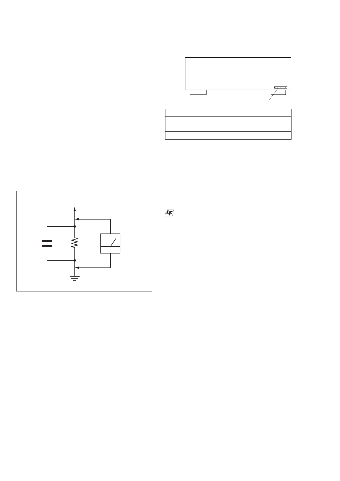
3. Measuring the voltage drop across a resistor by means of a
VOM or battery-operated AC voltmeter. The “limit” indication
is 0.75 V, so analog meters must have an accurate low-voltage
scale. The Simpson 250 and Sanwa SH-63Trd are examples
of a passive VOM that is suitable. Nearly all battery operated
digital multimeters that have a 2 V AC range are suitable. (See
Fig. A)
To Exposed Metal
Parts on Set
MODEL IDENTIFICATION
–BACK PANEL–
Part No.
Model Part No.
US
AEP
Canadian 4-408-213-2
4-408-213-0[]
4-408-213-1[]
[]
Notes on chip component replacement
• Never reuse a disconnected chip component.
• Notice that the minus side of a tantalum capacitor may be damaged by heat.
UNLEADED SOLDER
Boards requiring use of unleaded solder are printed with the leadfree mark (LF) indicating the solder contains no lead.
(Caution: Some printed circuit boards may not come printed with
the lead free mark due to their particular size)
AC
1.5 kΩ0.15 μF
Earth Ground
voltmeter
(0.75 V)
Fig. A. Using an AC voltmeter to check AC leakage.
: LEAD FREE MARK
Unleaded solder has the following characteristics.
• Unleaded solder melts at a temperature about 40 °C higher
than ordinary solder.
Ordinary soldering irons can be used but the iron tip has to be
applied to the solder joint for a slightly longer time.
Soldering irons using a temperature regulator should be set to
about 350 °C.
Caution: The printed pattern (copper foil) may peel away if the
heated tip is applied for too long, so be careful!
• Strong viscosity
Unleaded solder is more viscous (sticky, less prone to fl ow)
than ordinary solder so use caution not to let solder bridges
occur such as on IC pins, etc.
• Usable with ordinary solder
It is best to use only unleaded solder but unleaded solder may
also be added to ordinary solder.
SAFETY-RELATED COMPONET WARNING!
COMPONENTS IDENTIFIED BY MARK 0 OR DOTTED LINE
WITH MARK 0 ON THE SCHEMATIC DIAGRAMS AND IN
THE PARTS LIST ARE CRITICAL TO SAFE OPERATION.
REPLACE THESE COMPONENTS WITH SONY PARTS
WHOSE PART NUMBERS APPEAR AS SHOWN IN THIS
MANUAL OR IN SUPPLEMENTS PUBLISHED BY SONY.
2
ATTENTION AU COMPOSANT AYANT RAPPORT
À LA SÉCURITÉ!
LES COMPOSANTS IDENTIFIÉS PAR UNE MARQUE 0 SUR
LES DIAGRAMMES SCHÉMATIQUES ET LA LISTE DES
PIÈCES SONT CRITIQUES POUR LA SÉCURITÉ DE FONCTIONNEMENT. NE REMPLACER CES COM- POSANTS QUE
PAR DES PIÈCES SONY DONT LES NUMÉROS SONT DONNÉS DANS CE MANUEL OU DANS LES SUPPLÉMENTS
PUBLIÉS PAR SONY.

TABLE OF CONTENTS
1. DISASSEMBLY
1-1. Case ..................................................................................... 4
1-2. Back Panel Section ............................................................. 5
1-3. Front Panel Section ............................................................. 5
1-4. MAIN Board Section .......................................................... 6
2. TEST MODE ...................................................................... 7
3. FM TUNER CHECK ........................................................ 9
4. DIAGRAMS
4-1. Block Diagram – Main Section – ......................................11
4-2. Block Diagram – Display and Power Section – ............... 12
4-3. Printed Wiring Board – Main Board – .............................. 14
4-4. Schematic Diagram – Main Board 1/3 – .......................... 15
4-5. Schematic Diagram – Main Board 2/3 – .......................... 16
4-6. Schematic Diagram – Main Board 3/3 – .......................... 17
4-7. Printed Wiring Board – Display and
Power Key Board – ........................................................... 18
4-8. Schematic Diagram – Display and
Power Key Board – ........................................................... 19
4-9. Printed Wiring Board – Headphone, Thermal and
Tuner1 Board – ................................................................. 20
4-10. Schematic Diagram – Headphone, Thermal and
Tuner1 Board – ................................................................. 20
STR-DH130
5. EXPLODED VIEWS
5-1. Case Section ...................................................................... 26
5-2. Front Panel Section ............................................................ 27
5-3. Back Panel Section ............................................................ 28
5-4. Chassis Section .................................................................. 29
6. ELECTRICAL PARTS LIST ....................................... 30
3
STR-DH130
SECTION 1
DISASSEMBLY
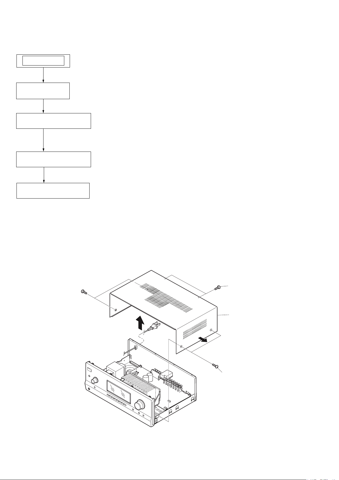
Note: This set can be disassemble according to the following sequence.
SET
1-1. CASE
(Page 4)
1-2. BACK PANEL SECTION
(Page 5)
1-3. FRONT PANEL SECTION
(Page 5)
1-4. MAIN BOARD SECTION
(Page 6)
Note: Follow the disassembly procedure in the numerical order given.
1-1. CASE
1 two
screws
(+BVST 4x8)
3 two
screws
(+BVTP 3x8)
4 case
2 two
screws
(+BVST 4x8)
4
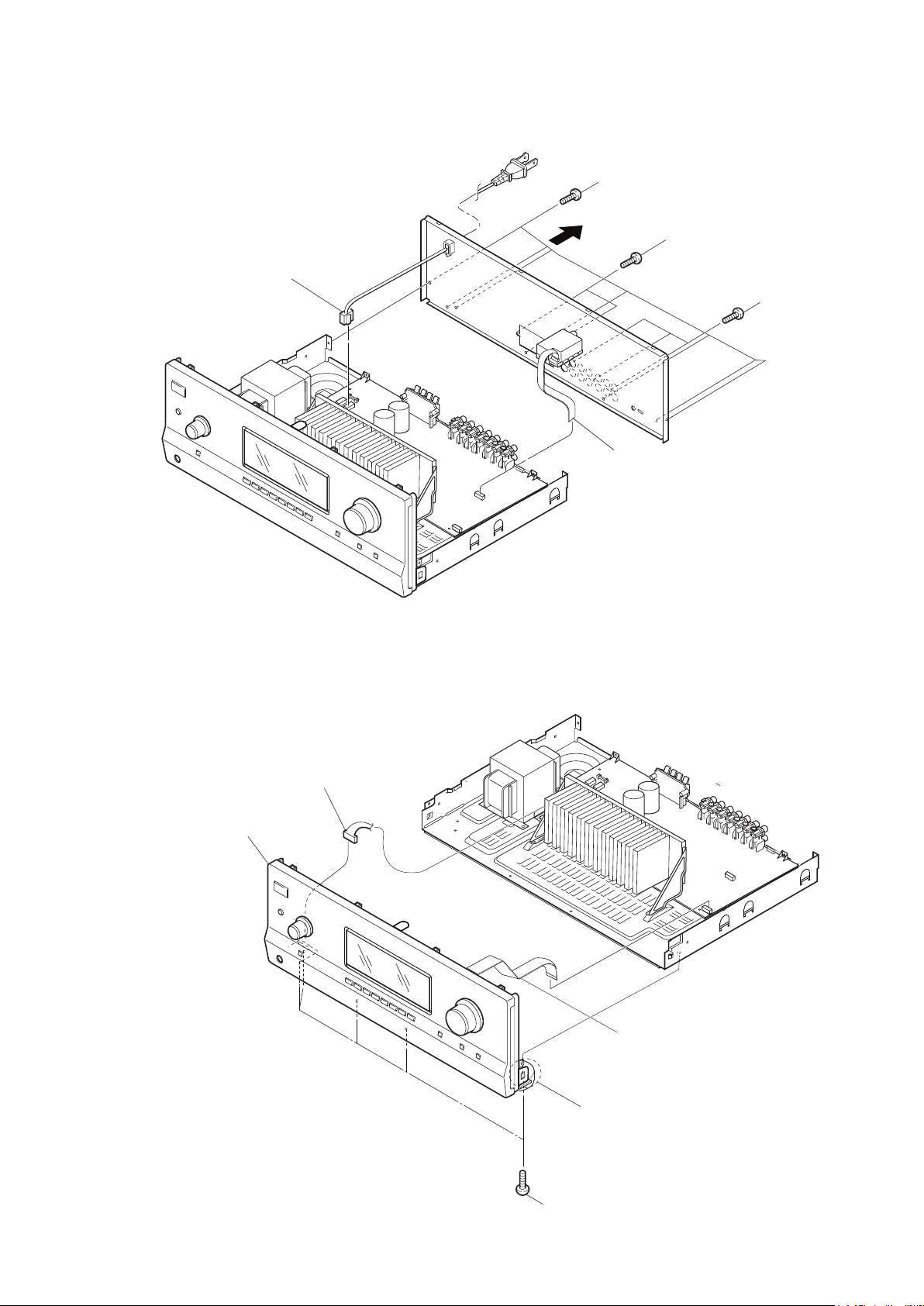
1-2. BACK PANEL SECTION
STR-DH130
1 CNP901 (3P)
5 seven
(+BVTP 3x8)
screws
4 two
screws
(+BVTP 3x8)
2 wire (flat type) (9 core)
(CNS402)
3 three
(+BVTP 3x8)
screws
1-3. FRONT PANEL SECTION
1 CNP790 (4P)
5 front panel section
2 wire (flat type) (15 core)
(CNS600)
4 claw
3 five
screws
(+BVTP 3x8)
5
STR-DH130
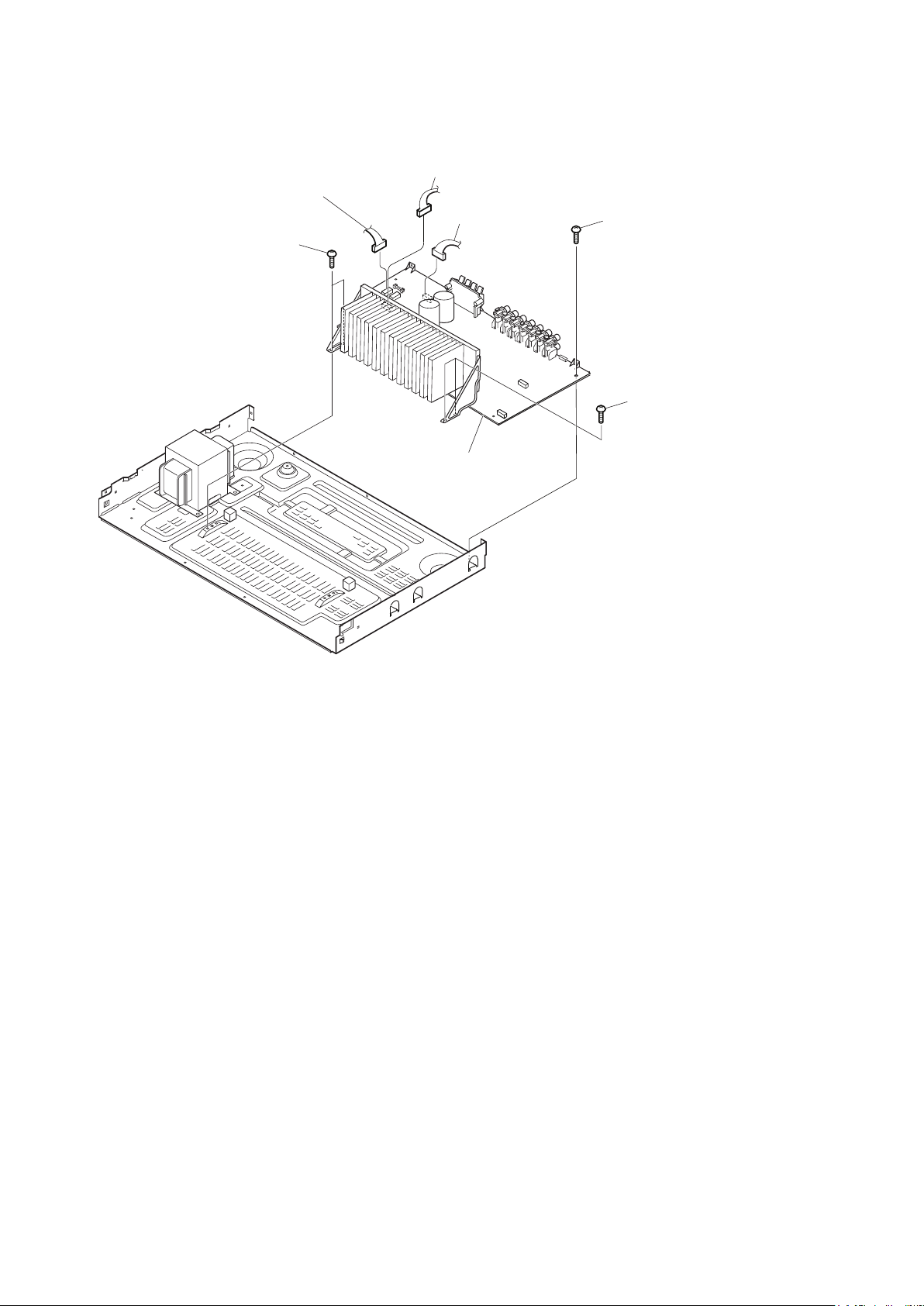
1-4. MAIN BOARD SECTION
2 CNP911 (5P)
1 CNP902 (2P)
5 two
screws
(+BVTP 3x8)
3 CNP930 (5P)
7 MAIN board section
4 one
screws
(+BVTP 3x8)
6 two
screws
(+BVTP 3x8)
6
SECTION 2
TEST MODE
STR-DH130
[AM CHANNEL STEP 9 kHz/10 kHz SELECTION MODE]
(US, Canadian model only)
* Either the 9 kHz step or 10 kHz step can be selected for the AM
channel step.
* Procedure:
1. While pressing the [TUNING MODE] button, press the
[
] button to turn on the main power.
?/1
2. The message “9K STEP” or “10K STEP” appears for a
moment
and the channel step is changed.
[SOFTWARE VERSION DISPLAY MODE]
* The software version is displayed.
* Procedure:
1. While pressing the [SPEAKERS (OFF/A/B/A+B)] and the
[MUTING] buttons simultaneously, press the [
] button to
?/1
turn on the main power.
2. The destination and the software version are displayed.
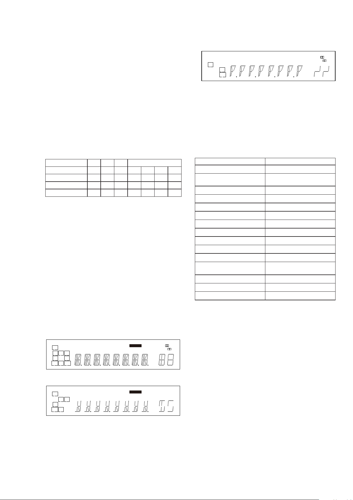
Destination D1 D2 D3 VERSION
UNKNOWN U N K
U2 U 2 1. 0 5 A
CA2 C A 2 2. 0 5 A
CEL C E L 3. 0 5 A
[KEY CHECK MODE]
* Button check
* Procedure:
1. While pressing the [SPEAKERS (OFF/A/B/A+B)] and the
[DIMMER] buttons simultaneously, press the [
] button to
?/1
turn on the main power.
2. The message “REST 13” appears.
3. Every press of any button other than the [
] counts down
?/1
the buttons. The buttons which are already counted once are
not counted again. When all buttons are pressed “REST 00”
appears.
[VACUUM FLUORESCENT DISPLAY TEST MODE]
* All fl uorescent segments are tested. When this test is activated,
all segments light on at the same time, then each segment lights
on one after another.
* Procedure:
While pressing the [SPEAKER (OFF/A/B/A+B)] and the
[DISPLAY] buttons simultaneously, press the [
] button to
?/1
turn on the main power.
1. ALL segments light on.
SW
LFE
LR
C
SL SR
S
SBL SB SBR
SP
SP B
HDMI
A
OPT
S-AIR
96/24
DTS
-ES
CAT
NEO:6COAX
SAT
MEMORY
D.RANGE
RDS
MONO
ZONE 2
SLEEP
dB
k
m
MHz
II
xPL
EXST
D
Hz
ft.
2. Turn the [INPUT SELECTOR] control, confi rm display.
LFE
LR
S
SP B
S-AIR
-ES
MEMORY
NEO:6COAX
SAT
ZONE 2
k
MHz
xPL
EXST
ft.
3. Turn the [INPUT SELECTOR] control, confi rm display.
SW
C
SL SR
SBL SB SBR
SP
HDMI
A
OPT
96/24
DTS
CAT
D.RANGE
RDS
MONO
SLEEP
dB
m
II
D
Hz
4. Turn the [INPUT SELECTOR] control, all segments light off.
[HISTORY MODE]
* The state that the set is used is memorized.
* Procedure:
1. While pressing the [TREBLE +] and [SPEAKERS (OFF/A/
B/A+B)] buttons, press the [
] button to turn on the power
?/1
and “HISTORY” is displayed.
2. Each time the []/[] buttons on the remote commander is
pressed, the item is switched in order as follows.
Item Display
History HISTORY
Count how many time of
protector happen
COUNT xx
Total single power on time xxxxxHxx01
Input function FUNCTION
HP ON/OFF HP xxx
Volume VOL xxx
Bass BASS xxx
Treble TREB xxx
Balance F xxx
Total power on time xxxxxHxx02
Muting MUTE xxx
Power on counter
(Rebox Test Mode)
REBXxxxx
Protector Type PROTxxxx
VACS step VACS xx
Return to history HISTORY
[PROTECTOR AUTO OFF]
* To disable auto off after protector occur
* Procedure:
1. While pressing the [TREBLE -] and [SPEAKERS (OFF/A/B/
A+B)] buttons, press the [
] button to turn on the main
?/1
power.
2. “PROT OFF” appears and switch off the set.
[SHIPMENT MODE]
* All preset contents are reset to the default setting.
* Procedure:
1. While pressing the [TUNING MODE] and the [MUTING]
buttons simultaneously, press the [
] button to turn on the
?/1
main power.
2. “CLEARING” and “CLEARED” appear and switch off the
set.
7

STR-DH130
[DESTINATION WRITE MODE]
* Write the set destination when the destination is “UNKNOWN”.
This mode can be performed once only.
* Procedure:
1. Press the [
2. Press the [FM MODE] and [DISPLAY] buttons
simultaneously.
3. “DEST XXX” appears and turns [INPUT SELECTOR] to
select the required destination.
4. Press [MEMORY/ENTER] button to save the destination.
5. “CLEARING” and “CLEARED” appear and the set will
switch on.
6. Perform [SOFTWARE VERSION DISPLAY MODE] to
confi rm the written destination.
] button to turn on the main power.
?/1
Selection Destination
DEST U2 U.S.A
DEST CEL Europe
DEST CA2 CANADA
8

SECTION 3
FM TUNER CHECK
STR-DH130
FM AUTO STOP CHECK
set
Procedure:
1. Turn on the set.
2. Input the following signal from Signal Generator to FM
antenna input directly.
* Carrier Frequency: A=87.5 MHz, B=98 MHz, C=108 MHz
Deviation : 75 kHz
Modulation : 1 kHz
ANT input : 35 dBu (EMF)
Note:
Please use 75 ohm “coaxial cable” to connect SG and the set. You
cannot use video cable for checking.
Please use SG whose output impedance is 75 ohm.
3. Set to FM tuner function and scan the input FM signal with
automatic scanning.
4. Confi rm that input Frequency of A, B and C are detected and
automatic scanning stops.
generator
OUT (75 Ω)
The stop of automatic scanning means “The station signal is received in good condition.”
9
STR-DH130
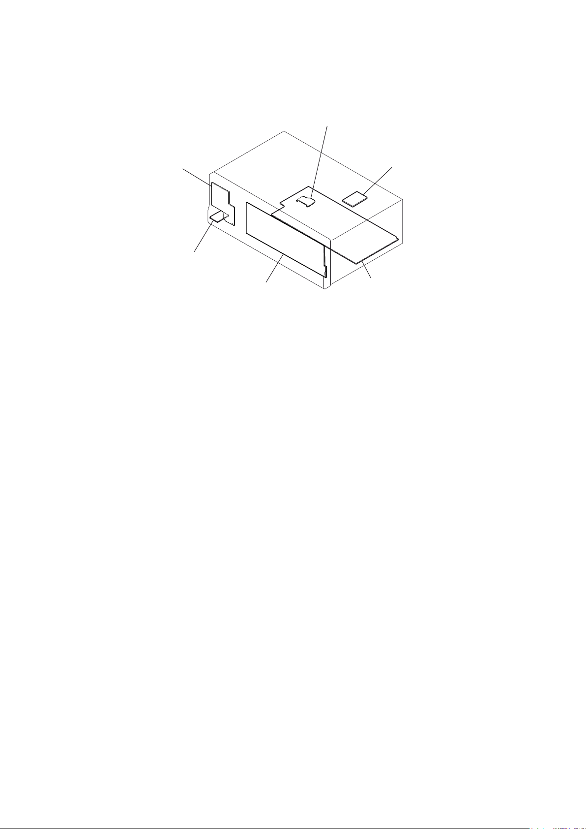
• Circuit Boards Location
SECTION 4
DIAGRAMS
THERMAL board
(for US and Canadian model only)
POWER KEY board
HEADPHONE board
DISPLAY board
TUNER1 board
MAIN board
10
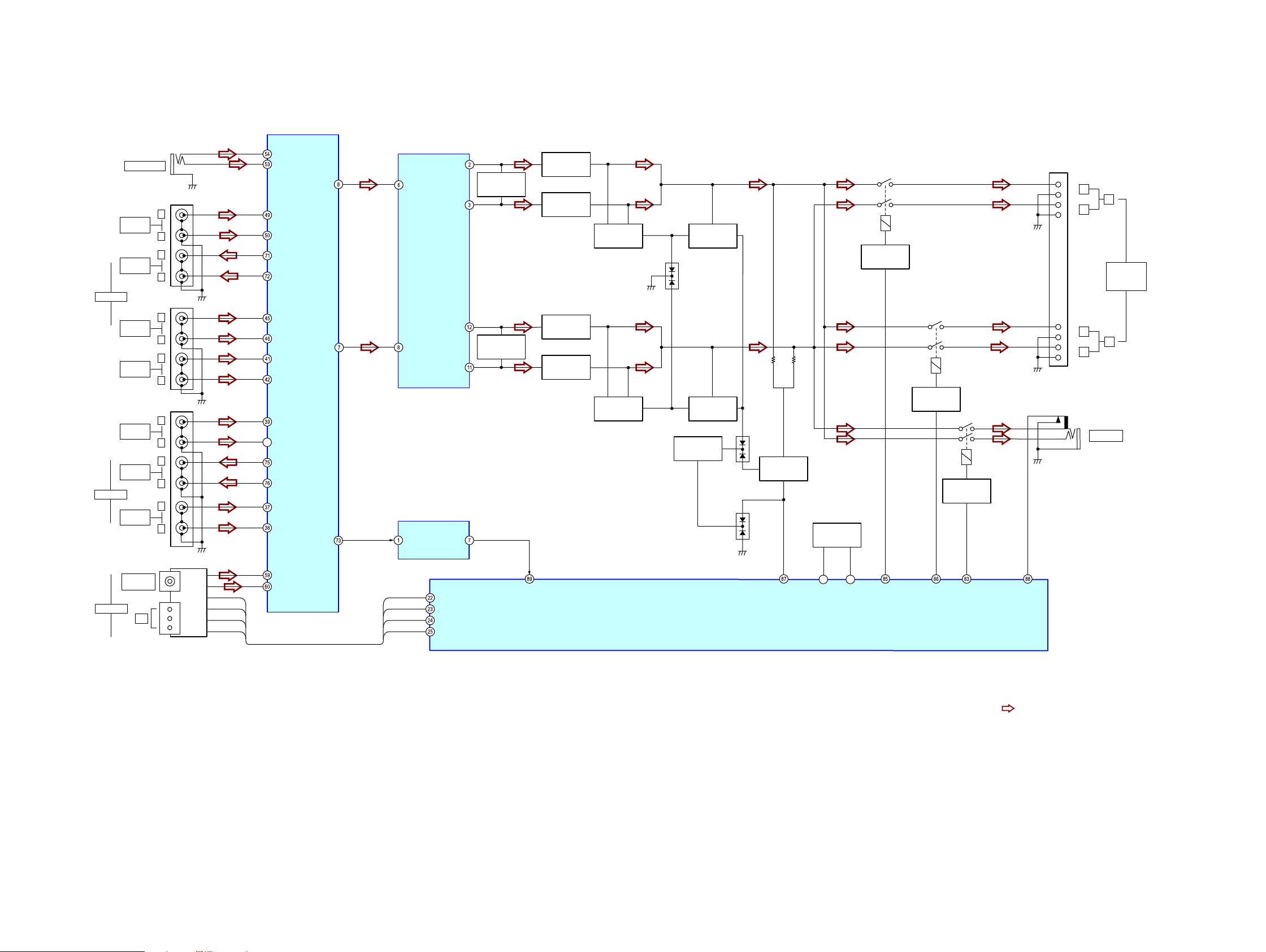
4-1. BLOCK DIAGRAM — MAIN SECTION —
J404
PORTABLE IN
J401
AUDIO
OUT
AUDIO
IN
SAT
AUDIO
OUT
AUDIO
IN
L
R
L
R
J402
L
R
L
R
J403
L
R
L
R
L
R
MD/TAPE
VIDEO
SA-CD/CD
AUDIO IN
AUDIO IN
BD-DVD
AUDIO IN
INR9
INL9
INL7
INR7
RECL1
RECR1
INL5
INR5
INL3
INR3
INL2
INR2
40
RECL3
RECR3
INL1
INR1
INPUT SELECTOR
IC400
OUTPUT L
OUTPUT R
REC L2
POWER AMP
IC700
IN1
IN2
SOUND DETECTOR
IC603
IN
+V OUT1
-V OUT1
+V OUT2
-V OUT2
OUT
LIMITER
Q701, Q702
LIMITER
Q751, Q752
BOOSTER
Q703
BOOSTER
Q704
BOOSTER
Q753
BOOSTER
Q754
OVERLAND
DETECTOR
Q711
OVERLAND
DETECTOR
Q761
D705
PROTECTOR
OVERLAND
DETECTOR
OVERLAND
DETECTOR
Q325
Q712
Q762
D326
D325
PROTECTOR
Q323, Q324
US, CND only
THERMAL
CIRCUIT
RELAY
DRIVE
Q350
RY350
RELAY
DRIVE
Q355
RY355
RELA
DRIVE
Q360
Y
RY360
J790
TB401
STR-DH130
+
L
-
+
-
+
-
+
-
R
L
R
A
B
PHONES
SPEAKER
INPEDANCE
USE 8-16:
ANTENNA
FM 75:
COAXIAL
AM
TUNER
AUDIO L
AUDIO R
RDS
INL 12
CK
DA
CE
CK
RDS
DA
CE
INR 12
CK
RDS
DA
CE
TUNER_SCL
TUNER_RDS
TUNER_SDA
TUNER_CE
SOUND DETECT
SYSTEM CONTROLLER
IC702 (1/2)
PROTECT
91
TEMP_SENSOR2
90
TEMP_SENSOR1
Y
SP_A_R
HP_RY
SP_B_RY
HP_DETECT
SLJnDl SDWK
: AUDIO
AEEUHYLDWLon
CND CDnDGLDn PoGHl
STR-DH130
11 11
 Loading...