

Sony SCP-C333ES Service Manual

SCD-C333ES
SERVICE MANUAL
Model Name Using Similar Mechanism NEW
CD Mechanism Type CDM59-DVBU5
Optical Pick-up Type KHM-230AAA/J1NP
SPECIFICATIONS
US Model
Canadian Model
When a super audio CD is played
Playing frequency range 2 Hz to 100 kHz
Frequency response 2 Hz to 50 kHz (–3 dB)
Dynamic range 103 dB or more
Total harmonic distortion rate
0.0015 % or less
Wow and flutter Value of measurable limit (±0.001 %
W. PEAK) or less
When a CD is played
Frequency response 2 Hz to 20 kHz
Dynamic range 99 dB or more
Total harmonic distortion rate
0.002 % or less
Wow and flutter Value of measurable limit (±0.001 %
W. PEAK) or less
Output connector
Load impedance
Over 10 kilohms
Light emitting
wave length:
( )
660 nm
75 ohms
ANALOG OUT
DIGITAL (CD)
OUT OPTICAL*
DIGITAL (CD)
OUT COAXIAL*
Jack type
Phono
jacks
Square
optical
output
connector
Coaxial
output
connector
Output level
2 Vrms
(at 50 kilohms)
–18 dBm
0.5 Vp-p
Load impedanceJack type Output level
PHONES
*Output only the audio signals of the CD
General
Laser radiant power: 5.47 uW at 650 nm
*These output is the value measured at a distance of about
200mm from the objective lens surface on the optical pick-up.
Power requirements 120 V AC, 60 Hz
Power consumption 28 W
Dimensions (w/h/d) 430 × 138 × 409 mm
Mass (approx.) 10.5 kg (23 lbs 3 oz.)
Supplied accessories
• Audio connecting cord
(phono jack × 2 y phono jack × 2) (1)
• Remote commander (remote) RM-SC300 (1)
• R06 (size-AA) batteries (2)
Design and specifications are subject to change without notice.
Stereo
phone jack
10 mW
(17 × 5 1/2 × 16 1/8 in.)
incl. projecting parts
32 ohms
SUPER AUDIO CD PLAYER

TABLE OF CONTENTS
SAFETY CHECK-OUT
1. SERVICING NOTES (1) .............................................3
2. GENERAL .......................................................................... 4
3. DISASSEMBLY
3-1. Cover ·············································································6
3-2. Front Panel Section ······················································· 6
3-3. Main Board···································································· 7
3-4. Audio Board ··································································7
3-5. CD Mechanism Deck (CDM59-DVBU5) ····················· 8
3-6. Optical Pick-Up Block (KHM-230AAA/J1NP)············ 9
3-7. Tab le Assy ·····································································9
3-8. Tray, Sensor Board ······················································ 10
3-9. Loading Motor Board ·················································· 10
3-10.Adjusting Phase of Swing Gear and Gear (U/D) ········ 11
4. DIAGRAMS
4-1. Block Diagrams ··························································· 13
• RF Section································································· 13
• Main Section-1·························································· 14
• Main Section-2·························································· 15
• Audio Section ···························································· 16
• Display/Power Section·············································· 17
4-2. Schematic Diagram RF Section ······························· 18
4-3. Printed Wiring Board RF Section······························19
4-4. Printed Wiring Board Main Section (Side A) ··········· 20
4-5. Printed Wiring Board Main Section (Side B)···········21
4-6. Schematic Diagram Main Section (1/5) ··················· 22
4-7. Schematic Diagram Main Section (2/5) ··················· 23
4-8. Schematic Diagram Main Section (3/5) ··················· 24
4-9. Schematic Diagram Main Section (4/5) ··················· 25
4-10. Schematic Diagram Main Section (5/5)··················· 26
4-11. Schematic Diagram Audio Section (1/3) ················· 27
4-12. Schematic Diagram Audio Section (2/3) ················· 28
4-13. Schematic Diagram Audio Section (3/3) ················· 29
4-14. Printed Wiring Board Audio Section (Side A) ········ 30
4-15. Printed Wiring Board Audio Section (Side B)········ 31
4-16. Schematic Diagram Display Section ······················· 32
4-17. Printed Wiring Board Display Section···················· 33
4-18. Schematic Diagram HP Section······························ 34
4-19. Printed Wiring Board HP Section ··························· 35
4-20. Schematic Diagram Sensor Section ························ 36
4-21. Printed Wiring Board Sensor Section ····················· 37
4-22. Schematic Diagram Power Section························· 38
4-23. Printed Wiring Board Power Section ·······················39
4-24. IC Block Diagrams ····················································· 41
4-25. IC Pin Function Description ·······································46
5. SERVICING NOTES (2) ................................................ 52
After correcting the original service problem, perform the following
safety checks before releasing the set to the customer:
Check the antenna terminals, metal trim, “metallized” knobs, screws,
and all other exposed metal parts for A C leakage. Check leakage as
described below.
LEAKAGE
The AC leakage from any exposed metal part to earth Ground and
from all exposed metal parts to any exposed metal part having a
return to chassis, must not exceed 0.5 mA (500 microampers).
Leakage current can be measured by any one of three methods.
1. A commercial leakage tester, such as the Simpson 229 or RCA
WT -540A. Follo w the manufacturers’ instructions to use these
instruments.
2. A battery-operated AC milliammeter. The Data Precision 245
digital multimeter is suitable for this job.
3. Measuring the voltage drop across a resistor by means of a
VOM or battery-operated AC v oltmeter . The “limit” indication
is 0.75 V, so analog meters must have an accurate lo w-v oltage
scale. The Simpson 250 and Sanwa SH-63Trd are e xamples of
a passive VOM that is suitable. Nearly all battery operated
digital multimeters that have a 2V AC range are suitable. (See
Fig. A)
To Exposed Metal
Parts on Set
0.15µF
1.5kΩ
Earth Ground
AC
voltmeter
(0.75V)
Fig. A. Using an AC voltmeter to check AC leakage.
SAFETY-RELATED COMPONENT WARNING !!
6. TEST MODE...................................................................... 53
7. EXPLODED VIEWS
7-1.Case Section··································································· 69
7-2.Front Panel Section ························································ 70
7-3.Main Chassis Section ····················································· 71
7-4.CD Mechanism (CDM59-DVBU5) -1 Section·············· 72
7-5.CD Mechanism (CDM59-DVBU5) -2 Section·············· 73
8. ELECTRICAL PARTS LIST ........................................ 74
2
COMPONENTS IDENTIFIED BY MARK 0 OR DOTTED LINE WITH
MARK 0 ON THE SCHEMATIC DIAGRAMS AND IN THE PARTS
LIST ARE CRITICAL TO SAFE OPERATION. REPLACE THESE
COMPONENTS WITH SONY PARTS WHOSE PART NUMBERS
APPEAR AS SHOWN IN THIS MANUAL OR IN SUPPLEMENTS
PUBLISHED BY SONY.
ATTENTION AU COMPOSANT AYANT RAPPORT
À LA SÉCURITÉ!!
LES COMPOSANTS IDENTIFIÉS P AR UNE MARQUE 0 SUR LES
DIAGRAMMES SCHÉMA TIQUES ET LA LISTE DES PIÈCES SONT
CRITIQUES POUR LA SÉCURITÉ DE FONCTIONNEMENT. NE
REMPLACER CES COMPOSANTS QUE PAR DES PIÈCES SONY
DONT LES NUMÉROS SONT DONNÉS DANS CE MANUEL OU
DANS LES SUPPLÉMENTS PUBLIÉS PAR SONY.

SECTION 1
SERVICING NOTES (1)
NOTES ON HANDLING THE OPTICAL PICK-UP BLOCK
OR BASE UNIT
The laser diode in the optical pick-up block may suffer electrostatic
break-down because of the potential difference generated by the
charged electrostatic load, etc. on clothing and the human body.
During repair, pay attention to electrostatic break-down and also
use the procedure in the printed matter which is included in the
repain parts.
The flexible board is easily damaged and should be handled with
care.
NOTES ON LASER DIODE EMISSION CHECK
The laser beam on this model is concentrated so as to be focused on
the disc reflective surface by the objective lens in the optical pickup block. Therefore, when checking the laser diode emission,
observe from more than 30 cm away from the objective lens.
The emission check enables continuous checking of the S curve.
CAUTION
Use of controls or adjustments or performance of procedures
other than those specified herein may result in hazardous
radiation exposure.
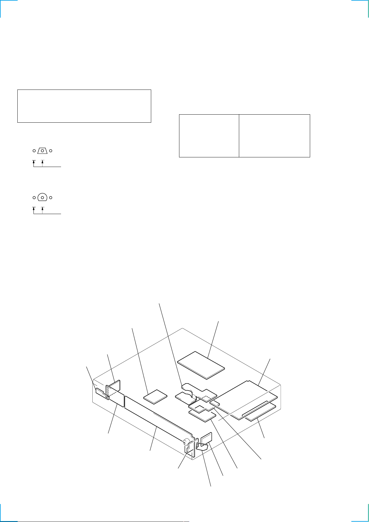
When the bottom plate is removed, the RF board can be checked.
eleven screws
(BVTP3 × 8)
bottom plate
RF board
This appliance is classified as a CLASS 1 LASER product.
The CLASS 1 LASER PRODUCT MARKING is located on the
rear exterior.
LASER DIODE AND FOCUS SEARCH OPERATION
CHECK
Carry out the “S curve check” in “CD section adjustment” and check
that the S curve waveform is output three times.
Notes on chip component replacement
• Never reuse a disconnected chip component.
• Notice that the minus side of a tantalum capacitor may be
damaged by heat.
Flexible Circuit Board Repairing
• Keep the temperature of soldering iron around 270˚C
during repairing.
• Do not touch the soldering iron on the same conductor of the
circuit board (within 3 times).
• Be careful not to apply force on the conductor when soldering
or unsoldering.
3

SECTION 2
GENERAL
Front Panel PartsDescriptions
POWER
DISC 1
CONTINUE
DISC 2
SHUFFLE
DISC 3
PROGRAM
DISC 4
MENU
DISC 5
TIME/TEXT
SACD
This section is extracted
from instruction manual.
CHECK CLEAR
AMS
DISC SKIPEX-CHANGE
PUSH ENTER
OPEN/CLOSE
LEVEL
MIN MAX
PHONES
1 POWER switch (11)
Press to turn on/off the player.
2 Remote sensor
(4)
3 DISC 1–5 button (12)
Press to select the disc.
4 SACD/CD button (with an LED) (10)
Each time you press the button while the Hybrid disc
(page 11) is loaded, the layer changes between an HD
layer (the LED turns on) and CD layer (the LED turns
off).
5 Display window (13)
Shows various information.
6 N button (12)
Press to start play.
N indicator
Lights up during playback.
7 X button (12)
Press to pause play.
X indicator
Lights up during pause.
8 x button (12)
Press to stop play.
9 EX-CHANGE button (15)
Press to replace discs while playing a disc.
0 CHECK button (19)
Press to check the programmed order.
qa lAMSL dial (AMS: Automatic Music Sensor)
(12)
When you turn the lAMSL dial
counterclockwise by one click, you go back to the
preceding track; when you turn the lAMSL dial
clockwise by one click, you go to the succeeding track.
qs CLEAR button (20)
Press to delete a programmed track number.
qd DISC SKIP button (11)
Press to select the disc.
qf PHONE LEVEL control
Adjust the headphones volume.
qg PHONES jack
Connect the headphones.
qh A OPEN/CLOSE button (11)
Press to open/close the disc tray.
qj Disc tray (11)
Press A OPEN/CLOSE to open/close the disc tray.
qk TIME/TEXT button (13)
Each time you press the button, the playing time of the
track, the total remaining time on the disc, or TEXT
information appears in the display.
ql MENU button (5)
Press to enter the menu.
w; PROGRAM button (19)
Press to select Program Play.
wa SHUFFLE button (18)
Press to select Shuffle Play.
w; CONTINUE button (12)
Press to resume normal play from Shuffle Play or
Program Play.
4

Rear Panel Parts Descriptions
L
R
ANALOG
OUT
COAXIALOPTICAL
OUT
DIGITAL (CD)
CONTROL
A1
ΙΙ
1 ANALOG OUT jacks (5)
Connect to an audio component using the audio
connecting cord.
2 DIGITAL (CD) OUT OPTICAL connector (5)
Connect to an audio component using an optical
digital cable.
3 DIGITAL (CD) OUT COAXIAL connector (5)
Connect to an audio component using the coaxial
digital cable.
Remote Parts Descriptions
1 CONTINUE button (12)
Press to resume normal play from Shuffle Play or
Program Play.
SHUFFLE button (18)
Press to select Shuffle Play.
PROGRAM button (19)
Press to select Program Play.
2 DIGITAL FILTER button (20)
Press to select the digital filter type when a CD is
played.
3 DISC/CAPS button (15, 23)
Press to select the disc.
Press to select the capital letter.
4 Number buttons (15)
Press to enter the track numbers.
5
i
10 button (16)
Press to locate a track numbered over 10.
6 REPEAT button (17)
Press repeatedly to play all tracks or only one track on
the disc.
7 NAME INPUT button (23)
Press to enter the name input mode.
8 H button (12)
Press to start play.
X button (12)
Press to pause play.
x button (12)
Press to stop play.
4 CONTROL A1
jack (5)
Connect to the Sony audio component using the
monaural (2P) mini-plug cord.
Note
Only the audio signals of the CD can be output from the
DIGITAL (CD) OUT connectors shown in 2 and 3. Those of
the Super Audio CD cannot be output through DIGITAL (CD)
OUT.
9 AMS ./> (AMS: Automatic Music Sensor)
buttons (16)
Press to locate a specific track.
0 m/M buttons (16)
Press to locate a portion you want to play within a
track.
qa DISC SKIP +/– buttons (11)
Press to select the disc.
qs CD1/2 (COMMAND MODE) switch (5)
Select the command mode.
qd DISPLAY MODE button (13)
Press to turn off the information.
qf TIME/TEXT/SPACE button (13, 23)
Each time you press the button, the playing time of the
track, the total remaining time on the disc, or TEXT
information appears in the display.
Press to insert a space.
qg ENTER button (23)
Press to decide the selection.
qh CLEAR button (19)
Press to delete a programmed track number.
qj CHECK button (19)
Press to check the programmed order.
qk SACD/CD button (10)
Each time you press the button while the Hybrid disc
(page 11) is loaded, the layer changes between an HD
layer (the SACD/CD LED turns on) and CD layer (the
SACD/CD LED turns off).
CD2
CD1
PLAY MODE
CONTINUE SHUFFLE
DIGITAL
FILTER
DISC
CAPS
PROGRAM
DISPLAY
MODE
TIME/TEXT
SPACE
ABC DEFABC
123
JKL MNOGHI
456
TUV WXYZPQRS
78
>10 ENTER
10/0
REPEAT CHECK
NAME
INPUT
–+
CLEAR
SACD/CD
AMS
DISC SKIP
9
5
SECTION 3
DISASSEMBLY
Note : Follow the disassembly procedure in the numerical order given.
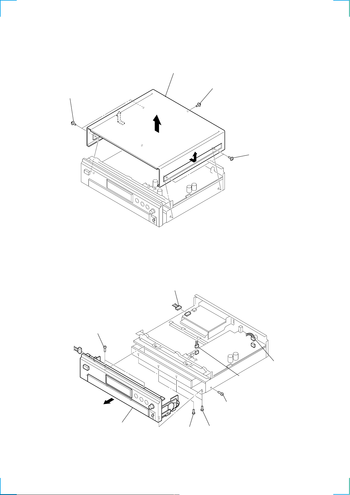
3-1. COVER
1 two screws(TP)
3 cover
2 screw(TP)
1 two screws(TP)
3-2. FRONT PANEL SECTION
6 two screws
(BVTP3 × 8)
8 front panel section
1 connector
(CN906)
5 two screws
(BVTP3 × 10)
3 connector
(CN303)
2 connector
(CN404)
7 screw
(BVTP3 × 8)
4 two screws
(BVTP3 × 8)
6

3-3. MAIN BOARD
)
8 two screws
(BVTP3 × 8)
9 MAIN board
6 connectors
(CN905)
1 connectors
(CN701)
7 two screws
(BVTP3 × 8)
2 wire (flat type) (35 core)
(CN503)
3 connectors
(CN904)
4 wire (flat type) (16 core)
(CN901)
5 wire (flat type) (8 core)
(CN902)
3-4. AUDIO BOARD
3 two screws
(BVTP3 × 8)
2 two screws
(BVTP3 × 8)
4 AUDIO board
1 four screws
(BVTP3 × 8
7
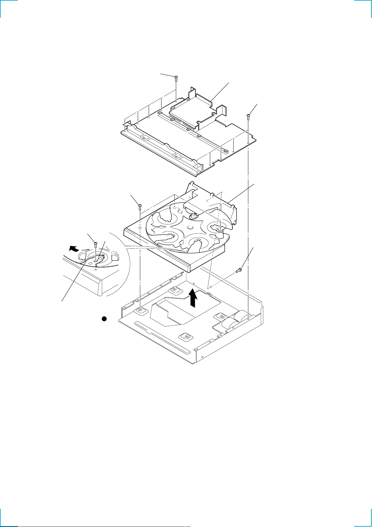
3-5. CD MECHANISM DECK (CDM59-DVBU5)
k
1 five screws
(BVTP3 × 8)
3 sub chassis
2 five screws
(BVTP3 × 8)
4 three screws
6 screw
(BVTP3 × 8)
5 Slide the tray until the screw
that fixes the table assy can be
seen through around hole
in the table assy.
(BVTP3 × 8)
a
8 CD mechanism dec
(CDM59-DVBU5)
7 screw(BVTP3 × 8)
8

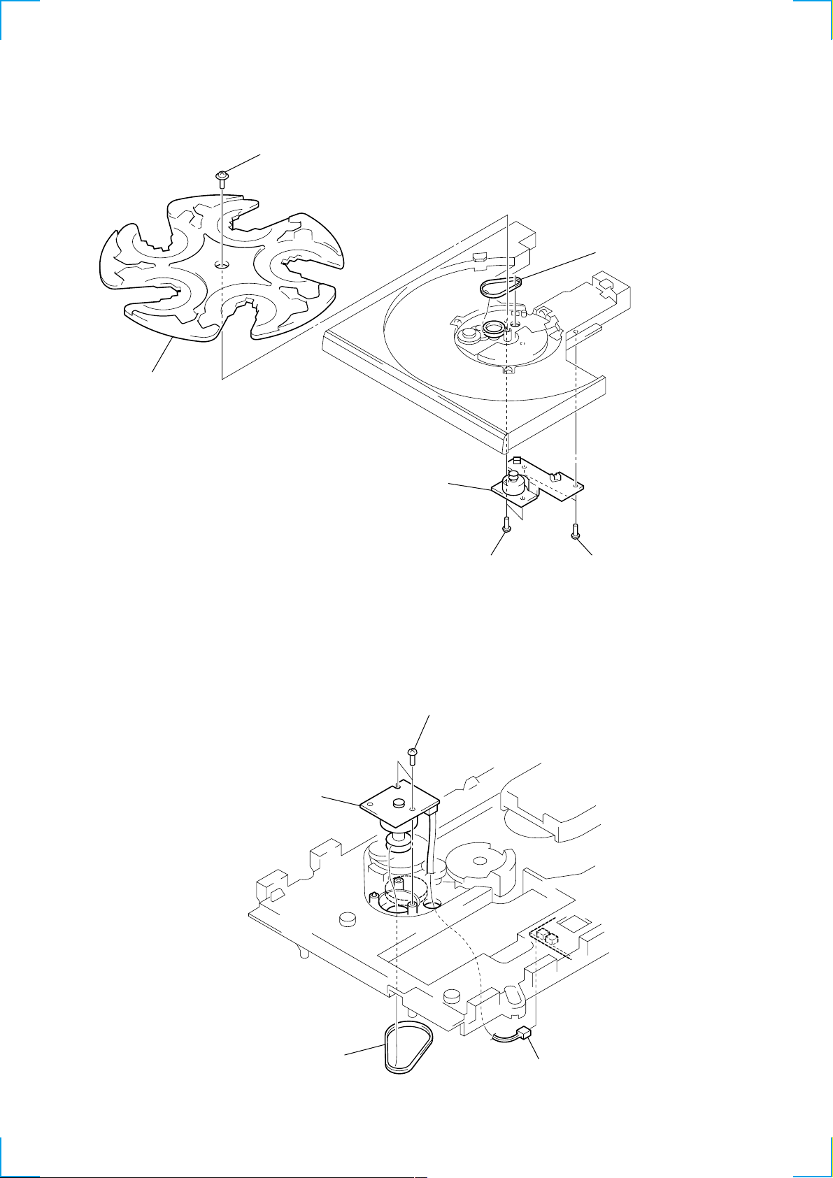
3-6. OPTICAL PICK-UP BLOCK (KHM-230AAA/J1NP)
Note: When installing the BU
on the chassis, set the
lever (lifter) in free
position, the gear (U/D)
in UP position, and insert
the shaft into the
groove of gear (U/D).
b
3-7. TABLE ASSY
3 two screws
gear (U/D)
9 three screws
(PTPWH M2.6)
BU section
b
(BTTP M2.6)
7 three screws
(BVTP3 × 8)
0 bracket (guide)
gear
(loading C)
2
3 two screws
(PTPWH M2.6)
4 optical pick-up block
(KHM-230AAA/J1NP)
5 four compression springs (932)
1 two screws
(PTPWH M2.6)
8 RF board
6 connector
(CN002)
7 two screws
(BTTP M2.6)
8 bracket (guide 2)
qa table assy
Note: When installing the table assy
on the chassis assy, engage
the gear (loading C) with the groove
by looking into the gear through
a hole in the table assy.
e
e
3
2 two screws
(BTTP M2.6)
1 Slide the tray until the screw
d
c
6 bracket (guide)
that fixes the bracket (guide)
can be seen through a round
c
hole , in the table assy.
4 wire (flat type)
(6 core) (CN15)
5 screw
(BTTP M2.6)
d
9
3-8. TRAY, SENSOR BOARD
)
2 tray
1 screw
(PTPWH M2.6)
3 belt (rotary)
5 SENSOR board
3-9. LOADING MOTOR BOARD
4 LOADING MOTOR board
4 two screws
(BTTP M2.6)
3 two screws
(BTTP M2.6)
4 two screws
(BTTP M2.6
10
1 belt (loading)
2 connector
(CN13)
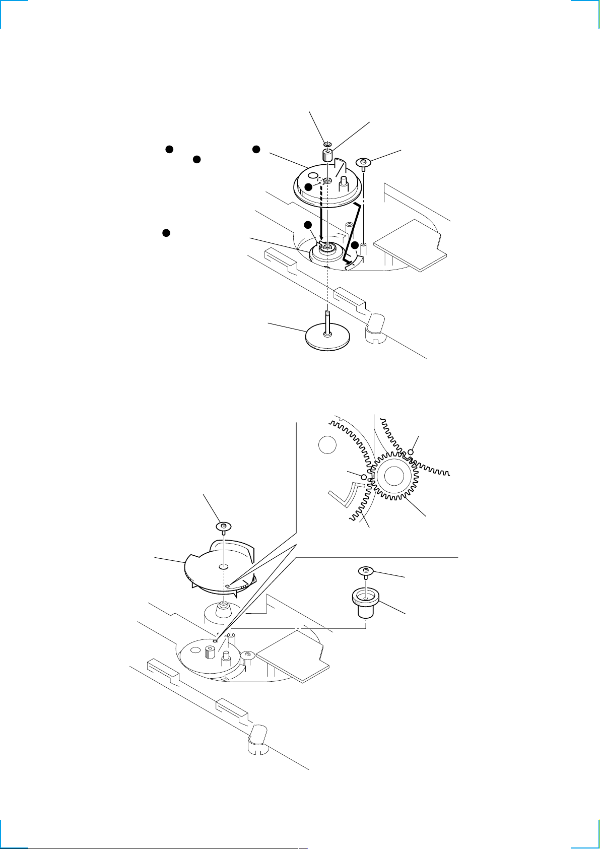
3-10. ADJUSTING PHASE OF SWING GEAR AND GEAR (U/D)
5 stopper washer (FR)
3 Let the swing gear through under the
chassis and engage its dowel
with the groove of rotary encoder.
h
f
g
g
4 Push fully the shaft of shaft gear and
align the hole shape of gear (loading B).
6 screw
(PTPWH M2.6)
2 Install the rotary encoder so that
its groove comes to the position
shown in the figure.
f
1 Insert the shaft gear up to the
position where its shaft comes
out by 5 mm.
8 screw
(PTPWH M2.6)
f
h
circle mark
circle mark
7 gear (U/D)
gear (RV)
swing gear
Fig. A
q; screw
(PTPWH M2.6)
9 gear (RV)
Note: Align swing gear, a circle mark
on the gear (U/D), and the teeth
of gear (RV) to the position
showing in the Fig. A.
11
SECTION 4
DIAGRAMS
NOTE FOR PRINTED WIRING BOARDS AND SCHEMATIC DIAGRAMS
Note on Printed Wiring Board:
• X : parts extracted from the component side.
• Y : parts extracted from the conductor side.
• b : Pattern from the side which enables seeing.
(The other layers' patterns are not indicated.)
Caution:
Pattern face side: Parts on the pattern f ace side seen from
(A Side) the pattern face are indicated.
Parts face side: Parts on the par ts face side seen from
(B Side) the parts face are indicated.
• Indication of transistor
Q
B
CE
These are omitted.
Q
B
CE
These are omitted.
Note on Schematic Diagram:
• All capacitors are in µF unless otherwise noted. pF: µµF
50 WV or less are not indicated except for electrolytics
and tantalums.
• All resistors are in Ω and 1/
specified.
f
•
• C : panel designation.
• 5 : fusible resistor.
• U : B+ Line.
• V : B– Line.
• Voltages and waveforms are dc with respect to ground
• Voltages are taken with a VOM (Input impedance 10 MΩ).
• Waveforms are taken with a oscilloscope.
• Circled numbers refer to waveforms.
• Signal path.
: internal component.
Note:
The components identified by mark 0 or dotted
line with mark 0 are critical for safety.
Replace only with part
number specified.
under no-signal conditions.
no mark : CD PLAY
Voltage var iations may be noted due to normal production tolerances.
Voltage var iations may be noted due to normal production tolerances.
J : SACD
c : CD
I : DIGITAL OUT
4
W or less unless otherwise
Note:
Les composants identifiés par
une marque 0 sont critiques
pour la sécurité.
Ne les remplacer que par une
pièce portant le numéro
spécifié.
• Circuit Boards Location
REMOTE SENSOR board
LOADING MOTOR board
AC SW board
KEY board
SENSOR board
DISPLAY board
HP board
MAIN board
AUDIO board
AC board
JUNCTION board
RF board
DOOR MOTOR board
12
DOOR SW board

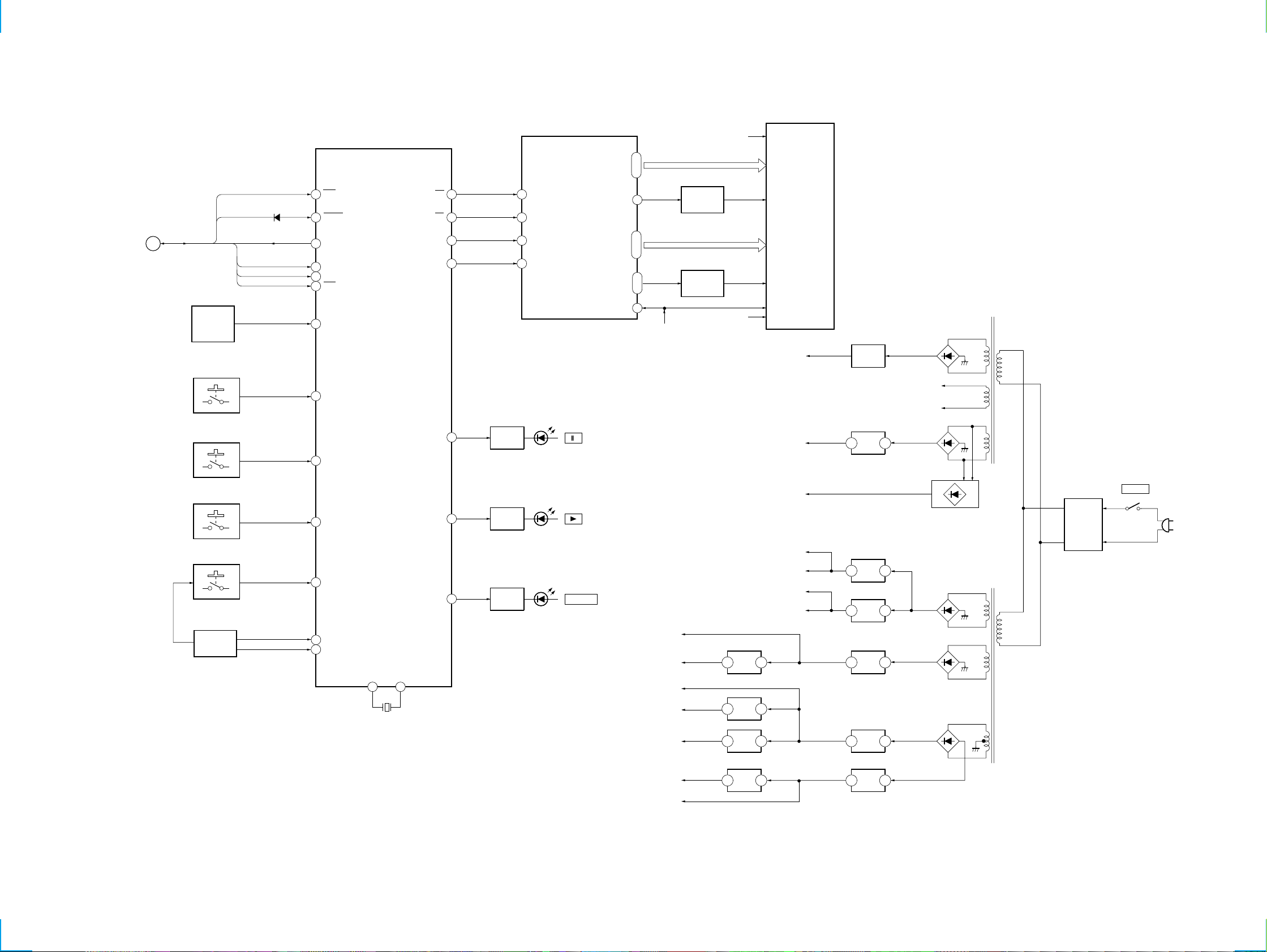
4-1. BLOCK DIAGRAMS
RF SECTION
OPTICAL PICK-UP
BLOCK
(KHM-230AAA/J1NP)
RF
A
B
C
D
DETECTOR
E
F
G
H
DVD_LD
LASER
DIODE
LASER
DIODE
(TRACKING)
(SLED)
INLIMIT
SENSOR
(SPINDLE)
M1000
(DOOR MOTOR)
VMOD
2-AXIS
DEVICE
M
M
M
VC
(2.5V)
(FOCUS)
DVD_PD
CD_LD
CD_PD
Q002
Q005
IC081
7
6
1
2
Q001
SACD-LD-DRIVE
Q003
CD-LD-DRIVE
1.65V
FD+
FD–
TD+
TD–
SD+
SD–
SP+
SP–
LOAD+
LOAD–
63
1
3
4
5
6
12
11
10
9
16
15
14
13
18
17
21
23
22
24
20
36
FOCUS/TRACKING COIL DRIVE,
12
11
14
13
17
18
8
9
6
5
IC502
SLED MOTOR DRIVE
FOCUS
COIL
DRIVE
TRACKING
COIL
DRIVE
SLED
MOTOR
DRIVE
IC512
SPINDLE/DOOR
MOTOR DRIVE
SPINDLE
MOTOR
DRIVE
DOOR
MOTOR
DRIVE
RFSIN
DVDRFP
A2
B2
C2
D2
A
B
C
D
CD_A
CD_B
CD_C
CD_D
CD_E
CD_F
DVDLD
DVDPD
CDLD
CDPD
VC
VC125
STANDBY1
STANDBY2
MUTE2
MUTE1
ATOP
62
ATON
61
FOCUS/TRACKING ERROR AMP
FFDR
5
FRDR
6
9
TFDR
2
TRDR
3
SFDR
24
SRDR
23
20
17
SP_ON
13
LOAD
22
MUTE_LOAD
2
59
60
SACD/CD RF-AMP
AIN
FNN
IC001
SPIN
SPDA
FNP
AIP
53
52
FJMP1
FJMP2
MUTE_2D
SCD-C333ES
54
DIP
RFAC
MIRR
SDATA
SCLK
LDON
SDEN
57
IC004(1/2)
VC-BUFFER
1.65V
IC509
CD-DECODER
SERVO-DSP
50
RFAC
40
TE
39
TE
FE
40
FE
PI
38
27
47
46
26
48
MIRR
DATA_RF
CLK_RF
LDON
SDEN
IC004(2/2)
57
PI
TE
MIRR
AVC(1.65V)
TFDR
TRDR
SFDR
SRDR
LIM_SW
SE
41
TE
FE
39
FE
PI
43
RFDC
20
MIRR
42
CE
38
VC
33
FFDR
34
FRDR
31
TFDR
32
TRDR
29
SFDR
30
SRDR
26
SSTP
DOUT
PCMD
BCK
LRCK
XTAI
WDCK
EXCK
SBSO
WFCK
C2PO
LOCK
FOK
COUT
SCOR
GFS
SCLK
SENS
CLOK
XLAT
DATA
MUTE
SQCK
SQSO
MD2
XRST
MDP
AVC 1.65V
64
66
67
65
71
17
80
79
10
14
24
22
19
15
13
8
7
6
5
4
3
77
76
63
2
25
MDAT
BCLK
LRCK
768FS
GSCOR
EXCK
SBSO
WFCK
C2PO
LOCK
FOK
COUT
SCOR
GFS
SCLK
SENS
CLOK
XLAT
DATA
MUTE_CD
SQCK
SQSO
MD2
XRST_CD
MDP
8
14
Q372
BUFFER
10
12
IC385
OPTICAL
TRANSMITTER
55
DIN
RFAC
+3.3V
• Signal Path
OPTICAL
COAXIAL
MDAT, BCK, LRCK
: SACD
: CD
: DIGITAL OUT
IC385
J385
SCOR
A
TO MAIN SECTION(1/2)
(Page 14)
DIGITAL OUT
CD
TO AUDIO SECTION
B
(Page 16)
C
TO MAIN SECTION(1/2)
(Page 14)
TO MAIN SECTION(2/2)
D
(Page 15)
TO MAIN SECTION(1/2)
E
(Page 14)
TO MAIN SECTION(1/2)
F
(Page 14)
TO MAIN SECTION(2/2)
G
(Page 15)
H
TO MAIN SECTION(2/2)
(Page 15)
VMOD
16
I
TO MAIN SECTION(2/2)
(Page 15)
1313

SCD-C333ES
MAIN SECTION-1
TO RF/SERVO SECTION
(Page 13)
TO MAIN SECTION(2/2)
(Page 15)
TO MAIN SECTION(2/2)
(Page 15)
TO MAIN SECTION(2/2)
(Page 15)
TO MAIN SECTION(2/2)
(Page 15)
TO RF/SERVO SECTION
(Page 13)
TO RF/SERVO SECTION
(Page 13)
TO RF/SERVO SECTION
(Page 13)
TO MAIN SECTION(2/2)
(Page 15)
TO MAIN SECTION(2/2)
(Page 15)
16
SP_DW
D0 – 7
A0 – 7
RF_AC
SP_DW
IC706
D-RAM
DATA BUS
ADDRESS BUS
MDP
SPIN
APDO
RF_AD_CE, WMPLCK
WE
RAS
UCAS
LCAS
JIT
A0 – 9
I/O0 – 15
OE
4
IC704
SW
21 – 24, 27 – 32
2 – 5, 7 – 10,
41 – 44, 46 – 49
17
33
18
34
35
IC708(2/2)
IC703(1/2)
2
1
IC708(1/2)
+
-
MA0 – 9
BD0 – F
D0 – 7
A0 – 7
XRST_DVD
XHRD
XHWR
XCS1882
XINIT0
XINIT1
SCOR
MDIN
GSCOR
EXCK
SBSO
WFCK
C2PO
BCLK
MDAT
LRCK
GFS_V
A
J
K
L
M
E
F
C
N
O
768FS
117
RFIN
89, 91
MA0 – 9
79 – 80, 82 – 87,
MD0 – F
104 – 106
66 – 69,71, 73 – 75,
96 – 97, 99, 101, 102,
76
XMWR
94
XMOE
XRAS
78
95
XCAS
D0 – 7A0 – 7
172 – 176, 1, 2, 45, 7, 9 – 14
164
XRST
17
XRD
18
XWR
XCS
19
XINT0
20
XINT1
21
150
SCOR
MDIN2
137
SPO
135
GSCOR
146
EXCK
147
SBIN
148
151
WFCK
155
C2PO
158
BCLK
160
MDAT
LRCK
163
GFS
107
APEO
109
IC701
DVD DECODER
XHWR
XHRD
XHRQ
HDB8
XHAC
MA11
MA10
XTAL
XTL2
XTL1
HDB0 – 7
48
49
46
26
53
93
92
167
169
170
32, 30, 27, 24
44, 41, 39, 35,
RF_AC
768FS
IC803
RF-BUFFER
31
RF_AC_CE
WMPLCK
2 – 9
SHIFT REGISTER
B
2
4
3
2
4
RF A/D CONVERTER
29
ADIN
5
XCE
24
2
IC812
BUFFER
IC815
IC813
BUFFER
IC814
IC804
IC806
IC807
• Signal Path
: SACD
100
17
99
80
81
13
10
11
14
5
2
1
6
7
8
9
91 – 98
SDCK
EXCKO1
XSHD
XSAK
SDEF
XSRQ
82 – 89
WCK
WRFD
SD0 – 7
WAD0 – 7
XRST
SMUTE
XMSLAT
MSCK
MSDI
MSDO
MSREDY
MCKI
IC801
DSD DECODER
PRAWN
DSAL
DSAR
XWE
XCAS
XRAS
XOE
BCKD
BCKA
SDATAL
47
SDATAR
48
IC808
D-RAM
A0 – 10
51, 52, 55 – 63
70 – 77
DQ0 – 7
66
67
68
69
42
46
3
9
12
128FSO
2
IC811
CLOCK
A0 – 10
10 – 13, 16 – 21, 9
DQ0 – 7
2 – 5, 24 – 27
6
WE
23
CAS
7
RAS
22
OE
IC809
TIMING
QQ
CK
D
Q
CK
D
IC810
IC300
COUNTER
65
2
LT64FSO
8
Q
11
4
256FSO IN
TO AUDIO SECTION
P
(Page 16)
18 – 11
QF
11
CK
8
16
17
18
2
9 – 16
D0 – 7
CLK
4
IC805
4
18
2
XRST_DSD
SHRMUT
XMSLAT
MSCK
MSDATI
MSDATO
SHRRDY
768FS
1414

MAIN SECTION-2
SCD-C333ES
TO RF/SERVO SECTION
(Page 13)
TO RF/SERVO SECTION
(Page 13)
TO RF/SERVO SECTION
(Page 13)
TO MAIN SECTION(1/2)
(Page 14)
TO MAIN SECTION(1/2)
(Page 14)
16
G
D
H
N
J
S1022
(IN_SW)
S1023
(OUT_SW)
FJMP1
FJMP2
SPDA
LOAD
APDO
WMPLCK
2
3
6
8
7
IC904
D/A CONV
AO3
AO4
AO7
AO9
AO8
1
IC910
DT
CLK
LD
MUTE_CD
DATA_RF
CLK_RF
MUTE_2D
SP_ON
MUTE_LOAD
SW
4
RF_AD_CE
17
16
15
MD2
SENS
LOCK
FOK
GFS
DATA
XLAT
COUT
SCLK
CLOK
SQCK
SQSO
SCOR
MIRR
LDON
2
GFS_V
SP_DW
IN_SW
OUT_SW
DATA BUS
ADDRESS BUS
D0 - D7
2 – 9
1D-8D
CLK
XOC
1Q-8Q
19 – 12
3,25,24,21,23,2,26,1
XCE
IC905
RESET
6
OUT
J381
CONTROL A1 II
IFSOO
IFSCO
Q381
SW
A7
3 14 1 15 2
2A
1B
IC909
DECODER
XIFCS
XCS2
1XG
Q901
2XG
1Y2
2Y0
XHWR
1A
61211
IC907
D-FF
1
89 – 96 14 – 21
A0 – A7 D0 – D7
7
FCS_JMP_4
8
FCS_JMP_3
5
DATA_DAC
6
CLK_DAC
4
LAT_DAC
IC901
MECHA-CON
TE
65
FE
PI
TE
67
FE
60
PI
DOCTRL
3
SENS_CD
9
75
LOCK_CD
FOK_CD
74
71
GFS_CD
DATA_CD
26
LAT_CD
27
29
COUT_CD
SCLK_CD
72
CLOK_CD
37
59
MUTE_CD
35
SQCK
SQSO
33
SCOR
34
SDATA_RF
83
82
SDCLOK_RF
MIRR
32
LDON
43
MUTE_2D
60
63
SP_ON
MUTE_LOAD
61
MON_DVD
25
76
RF_AD_CE
JIT
64
JIT
58
GFS_DVD
77
SP_DW
30
IN_SW
31
OUT_SW
XTAL EXTAL
40 41
X901
20MHz
XRD
XWR
XCS_DVD
INIT0_DVD
INIT1_DVD
XCS2
XCS_IO
XDIS_IO
TXD
RXD
RST
INIT_DF
LATCH_DF
SHIFT_DF
SCDATA_DF
MODE_DF
AMUTE
BUSY_DP
SDIN
SDOUT
SLK
REQ
MUTE_DSD
XMSLAT
SCK_DSD
SDOUT_DSD
SDIN_DSD
READY_DSD
EEP_SIO
EEP_SCL
T_SENS
A1IN
XHRD
85
XHWR
84
XCS1882
12
XINIT0
22
XINIT1
23
XCS2
10
XCS_IO
11
XDIS_IO
44
TXD
81
RXD
80
38 20
INIT
97
LATCH
98
SHIFT
99
DATA
100
MODE
1
AMUTE
2
IFBUSY
51
SIN1
52
53
SHRMUT
XMSLAT
MSCK
MSDATI
MSDATO
SHRRDY
5
6
T_SENS
IC903
EEPROM
SDA
SCL
IC906
54
56
45
46
50
49
48
47
78
79
24
28
A0 - A6
10 – 4 11–13,15–19
A0 - A6A7 - A14
IC908
S-RAM
2
IN
C
5
I/O1 - I/O8
D0 -D7
XOE
XWE
22
27
S901
XIFCS
5V
XHRD
XHWR
XRST_DVD
XDIS_IO
XHWR
XHRD
XCS_IO
XRST_DP
XRST_DSD
A1OUT
44 – 46
A0 – A2 D0 – D7
RST_DVD
20
XDIS
39
41
XWR
XRD
42
XCS
43
19
RST_DP
18
RST_DSD
16
A1OUT
28 – 30, 33 – 37
IC902
I/O EXPANDER
LOAD_IN
LOAD_OUT
TBLR
TBLL
D_SENS
OUT_SW
VMOD
RST_CD
PD6
DATA BUS
ADDRESS BUS
15
13
7
6
11
S1
12
S2
10
59
22
21
26
M12V
Q903
Q904
OUT_SW_CHG
VMOD
XRST_CD
SDEN
LOADING/TABLE
2
3
7
16
Q902(1/2)
Q902(2/2)
IC920
+7V
1 3
REG
IC11
MOTOR DRIVE
OUT1+
FIN1
RIN1
OUT1-
OUT2+
FIN2
OUT2-
RIN2
8
9
11
10
D0 -D7
A0 - A7
TXD
RXD
M7V
M
(LOADING)
M
(TRAY)
S200
(TABLE ADDRESSS DETECT)
ROTARY
ENCODER
D11
(DISC SENSOR)
OPEN
CLOSE
S11
D10
(TABLE SENSOR)
TO MAIN SECTION(1/2)
K
(Page 14)
TO MAIN SECTION(1/2)
L
(Page 14)
TO MAIN SECTION(1/2)
M
(Page 14)
RS-232C (JIG)
M10
M11
I
TO RF/SERVO SECTION
(Page 13)
O
TO MAIN SECTION(1/2)
(Page 14)
TO DISPLAY/POWER SECTION
Q
R
(Page 17)
TO AUDIO SECTION
(Page 16)
1515

SCD-C333ES
AUDIO SECTION
TO RF/SERVO SECTION
(Page 13)
TO MAIN SECTION(1/2)
(Page 14)
IC101
IC301
DIGITAL FILTER
B
P
MDAT
BCLK
LRCK
SDATA L
SDATA R
48
49
50
53
52
DATAI
BCKI
LRCKI
SDATA L
SDATA R
L1 (–)
L1 (+)
L2 (+)
L2 (–)
1
3
6
8
28
27
25
24
IC100
CURRENT PULSE D/A
IN2–
IN2+
IN1+
IN1–
I01+
I02–
I01–
I02+
L+
1
2
4
5
L-
CONVERSION
6
2
I-V
Q100
7
1
Q101
IC102(1/2)
AUDIO FILTER
3
2
IC102(2/2)
BUFFER
+
1
-
6
-
+
5
7
RY350
R
J301
ANALOG OUT
L
TO MAIN SECTION(2/2)
(Page 15)
LT64FSO
256FSO IN
R
INIT
LATCH
SHIFT
DATA
MODE
51
44
30
28
31
32
33
34
SBCKI
LVCK02
INIT
NREGCLR
LATCH
SHIFT
SCDATA
MODE
3
IC302
IC200
CURRENT PULSE D/A
R-
17
R2 (–)
R2 (+)
19
R1 (+)
22
R1 (–)
XIN
13
5
24
IN2– IO1+
28
27
IN2+
25
IN1+
24
IN1–
IO2–
IO1–
IO2+
1
2
4
5
R+
CONVERSION
6
2
IC201
I-V
Q201
7
1
Q200
IC307(1/2)
HEADPHONE
AMP
5 7
IC202(1/2)
AUDIO FILTER
2
-
+
3
IC307(2/2)
HEAD PHONE
AMP
RV1101-1
PHONE LEVEL
J1101
PHONES
Q370
MUTING
IC202(2/2)
BUFFER
1
-
6
5
7
+
• Signal Path
: SACD
: CD
X321
45MHZ
AMUTE
16
Q350
MUTE
3
1
MUTING
CONTROL
RELAY
DRIVE
Q352
Q351
Q360
MUTING
RV1101-2
PHONE LEVEL
1616
DISPLAY/POWER SECTION
TO MAIN SECTION(2/2)
(Page 15)
Q
IC1000
REMOTE
CONTROL
RECEIVER
S1013, 1015, 1017,
1019, 1021
S1000(1/2), 1012, 1014,
1016, 1018, 1020
S1003, 1005, 1007,
1010, 1011
S1004, 1006, 1008
S1009
ROTARY
ENCODER
XFRRST
IFBSY
SIN1
IFSO0
IFSCO
XIFCS
D1002
IC1002
DISPLAY CONTROLLER
47 51
ACK
30
RESET
50
SOUT
49
SIN
48
SCK
REQ
60
56
SIRCS
45
KEY 3
44
KEY 2
43
KEY 1
42
KEY 0
40
JOG2
39
JOG1
EXTAL XTAL
32
31
X1000
CP
CS
DA
RESET OUT
LED(PAUSE)
LED(PLAY)
LED(SACD/CD)
SCD-C333ES
IC1001
FLUORESCENT
INDICATOR TUBE DRIVE
1 – 3452 – 39
P1 – 343G – 16G
+5V
+3.3V
+12V
+5V
+5V
Q1001
SEGMENT
DRIVE
Q1000, 1002
GRID
DRIVE
63
FL CLK (CL)
52
53
46
67
66
65
Q1006
LED
DRIVER
Q1005
LED
DRIVER
Q1004
LED
DRIVER
62
FLT (CE)
64
FL DATA (DI)
61
FL RST
D1001
D1000
S1000(1/2)
SACD/CD
VFL
P35
35
53, 54
1G, 2G
35
-31V
(DF+5V)
F1
FL1000
FLUORESCENT
INDICATOR
TUBE
T901
POWER
F2
D402- 405
-31V
+12V
(M12V)
C+12V
D+5V
A+5V
D+3.3V
A+3.3V
IC303
+3.3V
3
3
3
REG
IC304
+5V
REG
IC306
+5V
REG
1
1
1
Q401
-31V REG
IC400
+12V
3
REG
IC402
3
REG
IC401
+3.3V
3
REG
IC403
3
REG
IC405
+12V
3
REG
+5V
+5V
F1
F2
D406- 409
1
D432- 433,
D434
1
D410- 413
1
D414- 417
1
D422- 425
1
TRANSFORMER
T902
POWER
TRANSFORMER
L991
LINE
FILTER
S1025
POWER
AC
IN
IC305
-7V
16
-12V
-7V
3
REG
2
IC404
-12V
3
REG
2
1717

SCD-C333ES
4-2. SCHEMATIC DIAGRAM RF SECTION • Refer to page 40 for Waveforms.
1818
SCD-C333ES
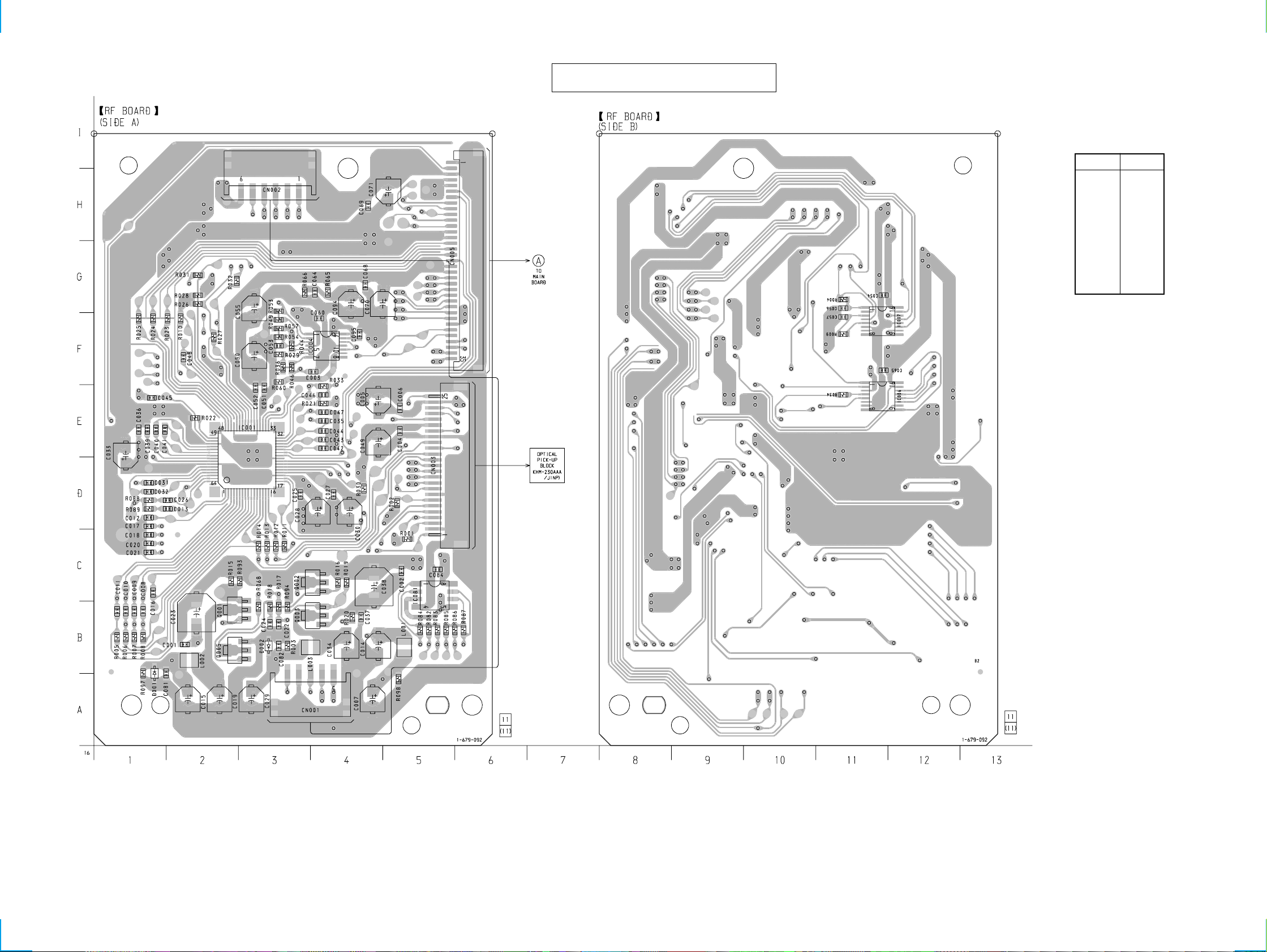
4-3. PRINTED WIRING BOARD RF SECTION • Refer to page 12 for Circuit Board Location.
There are a few cases that the part printed on
this diagram isn’t mounted in this model.
(Page 20)
• Semiconductor
Location
Ref. No. Location
D001 A-1
D002 B-3
IC001 E-3
IC004 F-4
IC081 C-5
Q001 B-2
Q002 C-3
Q003 B-3
Q005 B-2
1919

SCD-C333ES
4-4. PRINTED WIRING BOARD MAIN SECTION (SIDE A) • Refer to page 12 for Circuit Board Location.
(Page 30)
• Semiconductor
(Page 30)
Location
Ref. No. Location
D901 C-5
D902 C-5
D903 I-11
IC509 F-6
IC701 F-10
IC704 G-9
IC801 B-10
IC803 D-8
IC804 C-8
IC901 B-3
IC902 C-6
IC905 D-5
IC907 B-5
IC909 B-5
Q901 C-5
Q905 C-5
There are a few cases that the part printed on
this diagram isn’t mounted in this model.
(Page 19)
(Page 30)
(Page 33)
(Page 35)
(Page 30)
(Page 30)
(Page 37)
2020
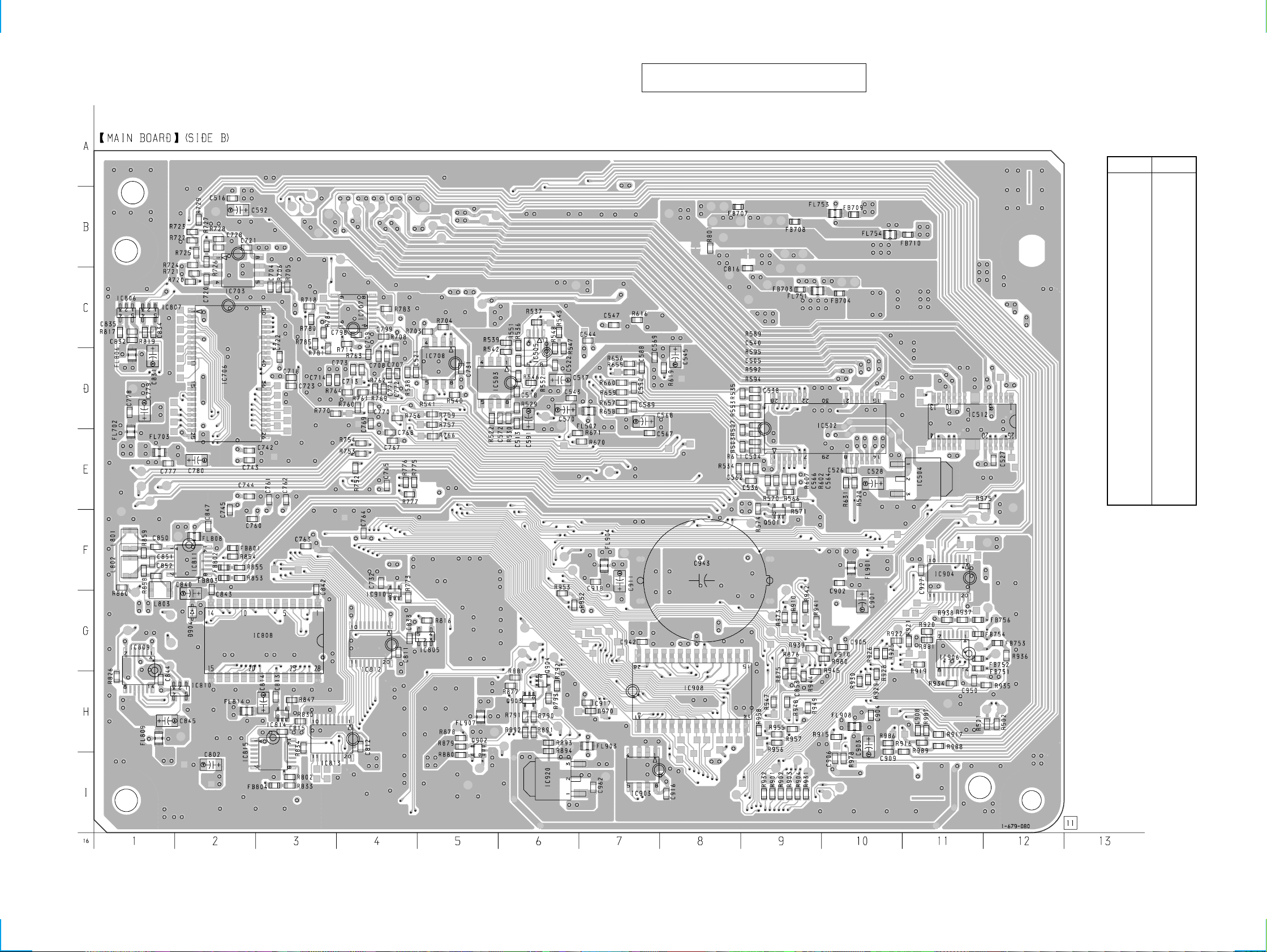
SCD-C333ES
4-5. PRINTED WIRING BOARD MAIN SECTION (SIDE B) • Refer to page 12 for Circuit Board Location.
There are a few cases that the part printed on
this diagram isn’t mounted in this model.
• Semiconductor
Location
Ref. No. Location
D904 G-2
IC502 D-9
IC503 D-5
IC504 E-11
IC512 D-11
IC703 C-2
IC706 D-2
IC708 D-5
IC805 G-5
IC806 C-1
IC807 C-1
IC808 G-3
IC809 G-1
IC810 H-2
IC811 C-2
IC812 G-4
IC813 H-3
IC814 H-3
IC815 I-3
IC903 I-7
IC904 F-11
IC906 G-11
IC908 G-8
IC910 G-4
IC920 I-6
Q902 H-5
Q903 H-6
Q904 H-6
2121
SCD-C333ES
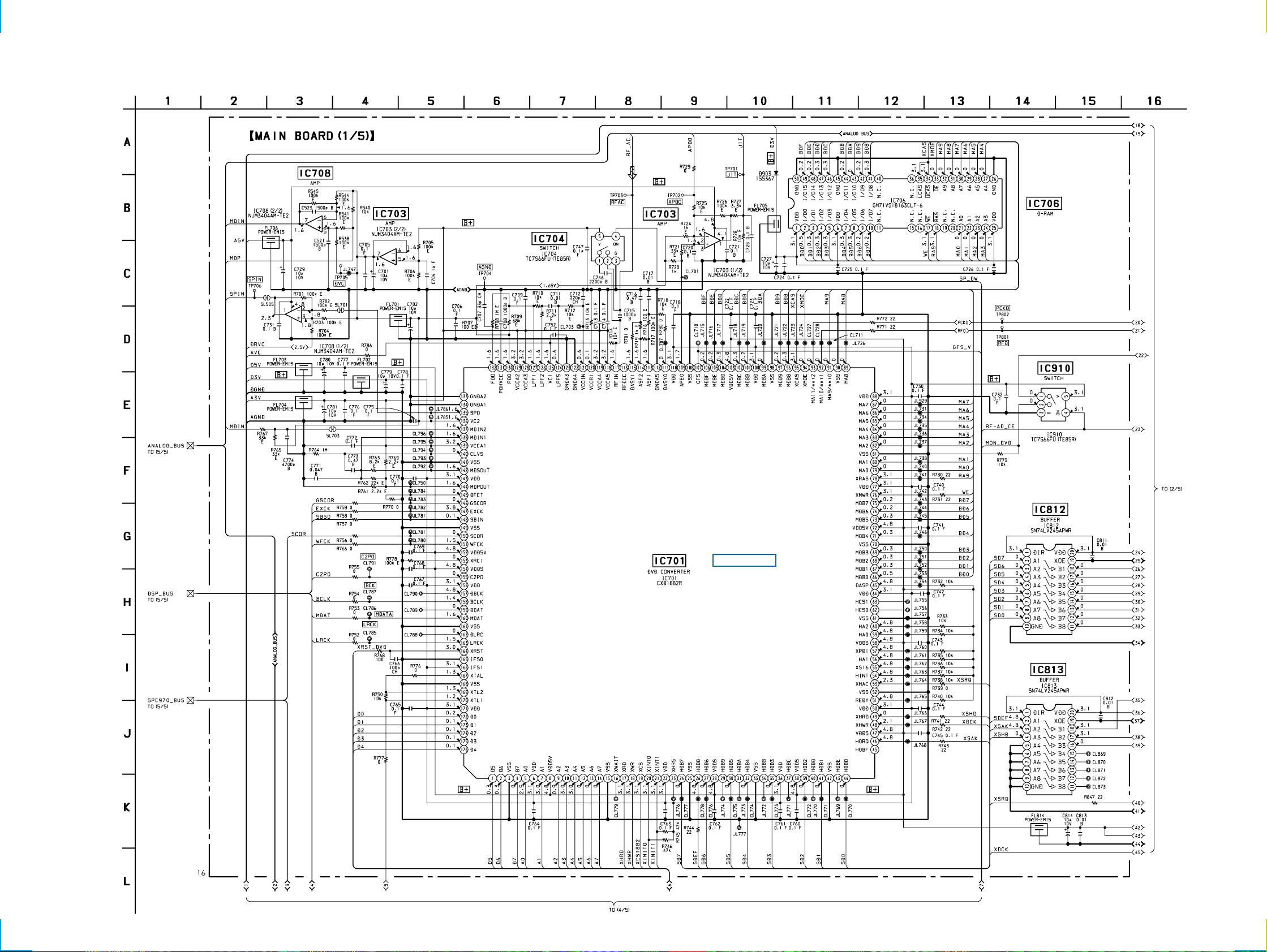
4-6. SCHEMATIC DIAGRAM MAIN SECTION (1/5) • Refer to page 49 for IC Pin Function.
PIN FUNCTION
2222
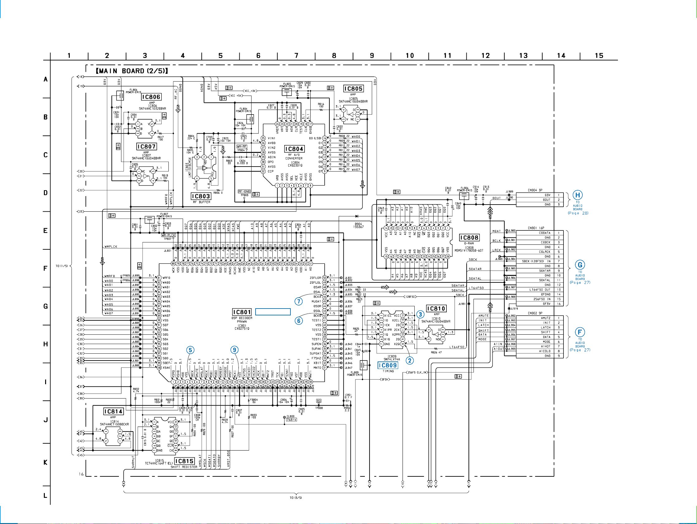
4-7. SCHEMATIC DIAGRAM MAIN SECTION (2/5) • Refer to page 40 for Waveforms. • Refer to page 41 for IC Block Diagrams. • Refer to page 46 for IC Pin Function.
SCD-C333ES
PIN FUNCTION
2323
SCD-C333ES
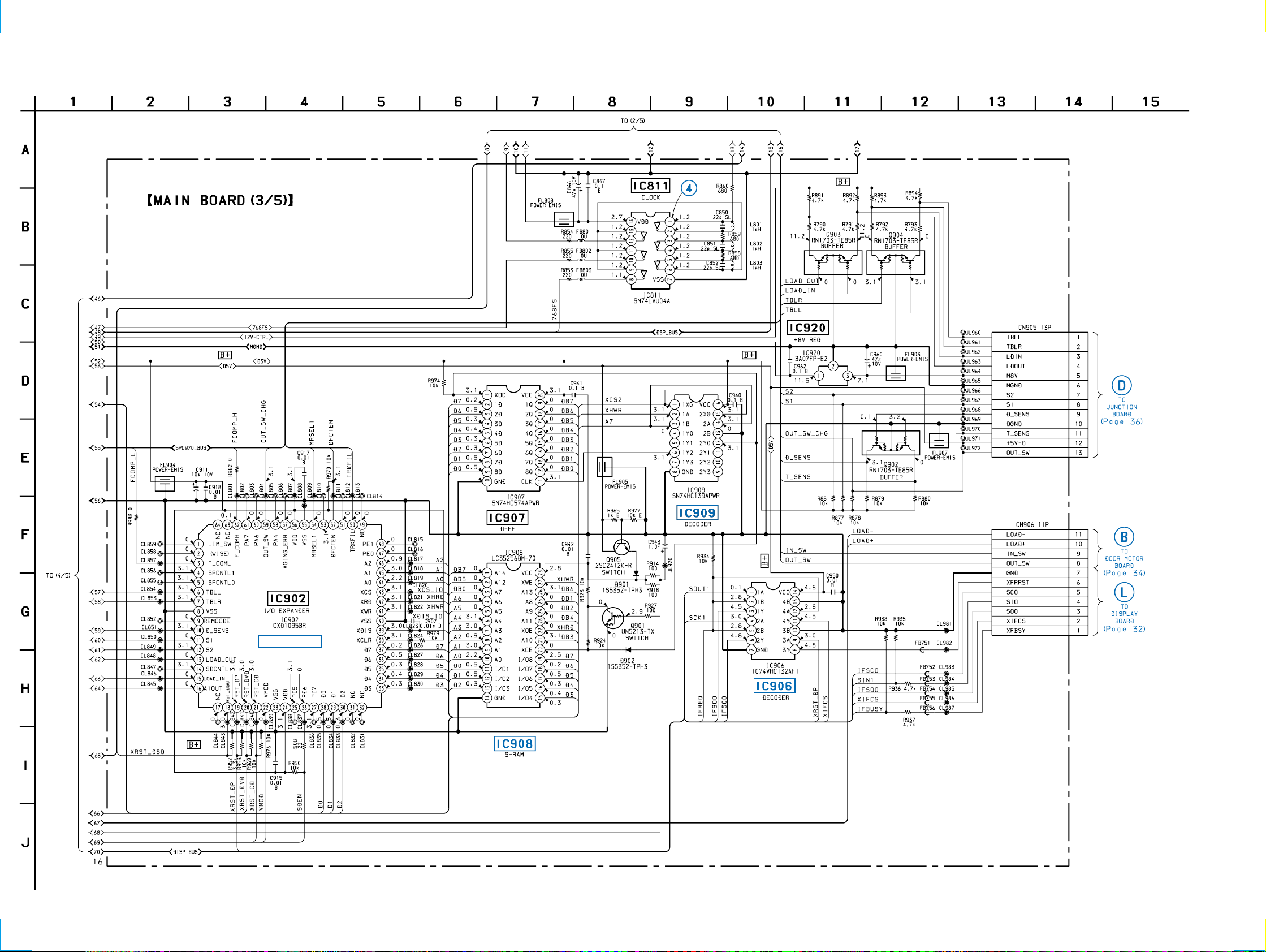
4-8. SCHEMATIC DIAGRAM MAIN SECTION (3/5) • Refer to page 40 for Waveform. • Refer to page 41 for IC Block Diagrams. • Refer to page 48 for IC Pin Function.
PIN FUNCTION
2424

4-9. SCHEMATIC DIAGRAM MAIN SECTION (4/5) • Refer to page 40 for Waveform. • Refer to page 42 for IC Block Diagrams.
SCD-C333ES
2525

SCD-C333ES
4-10. SCHEMATIC DIAGRAM MAIN SECTION (5/5) • Refer to page 40 for Waveform. • Refer to page 43 for IC Block Diagrams.
2626
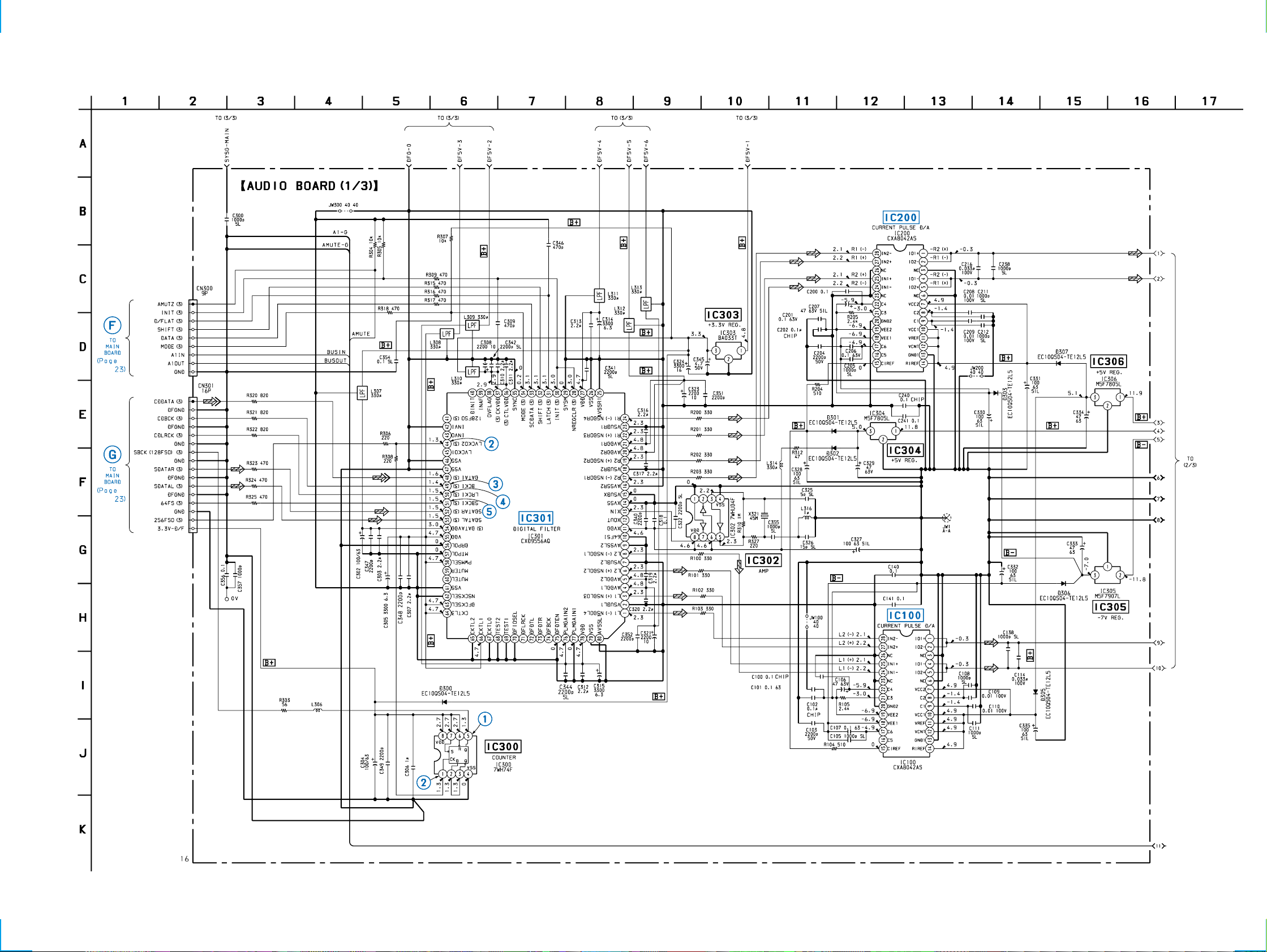
4-11. SCHEMATIC DIAGRAM AUDIO SECTION (1/3) • Refer to page 40 for Waveforms. • Refer to page 44, 45 for IC Block Diagrams.
SCD-C333ES
2727
 Loading...