

Page 1
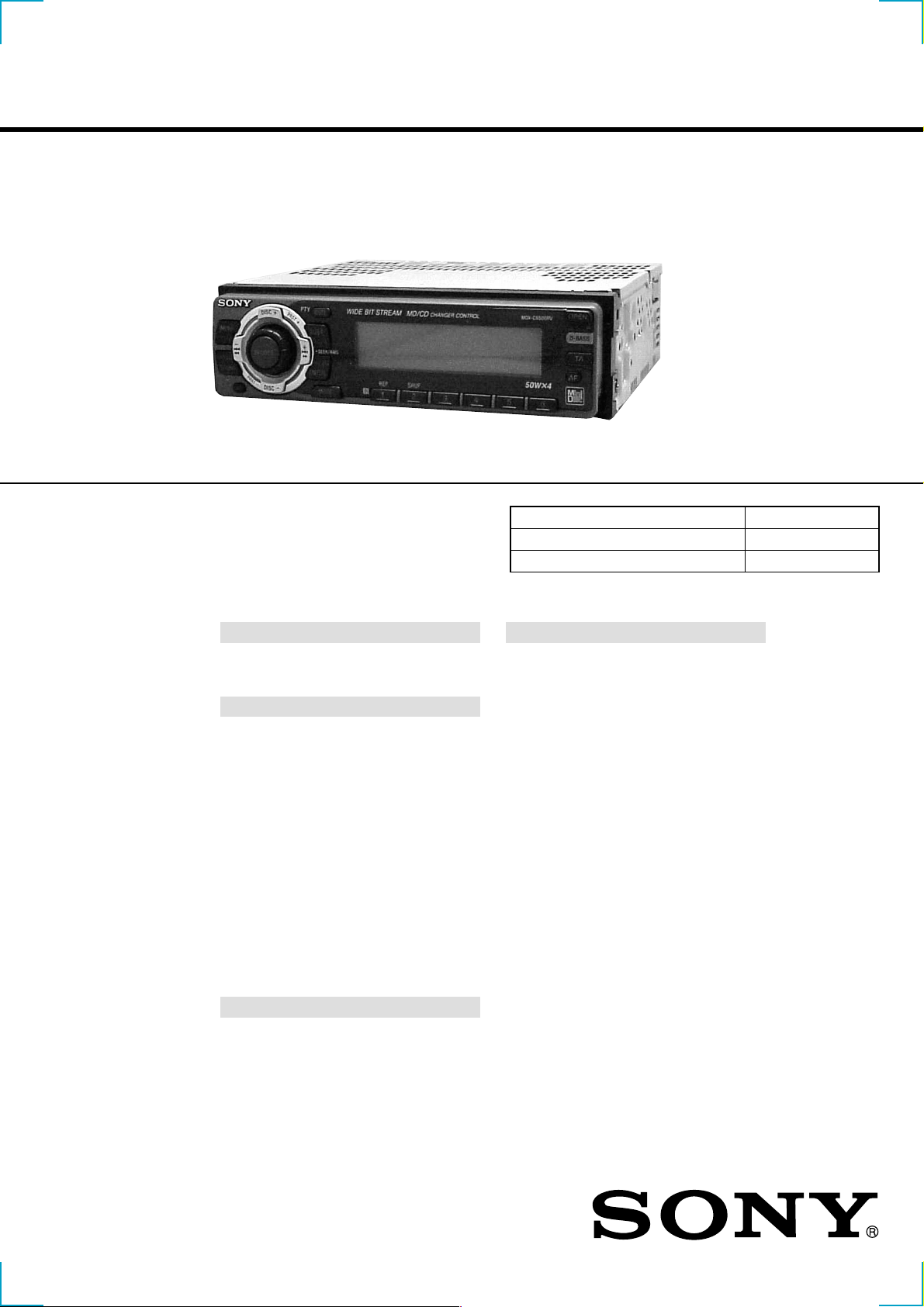
MDX-C6500RV
SERVICE MANUAL
Ver 1.1 2001.05
SPECIFICATIONS
AEP Model
UK Model
Model Name Using Similar Mechanism MDX-C6500R
Base Mechanism Type MG-164NZ-138
Optical Pick-up Name KMS-241C/J1NP
MD player section
Signal-to-noise ratio 90 dB
Frequency response 10 – 20,000 Hz
Wow and flutter Below measurable limit
Tuner section
FM
Tuning range 87.5 – 108.0 MHz
Aerial terminal External aerial connector
Intermediate frequency 10.7 MHz/450 kHz
Usable sensitivity 8 dBf
Selectivity 75 dB at 400 kHz
Signal-to-noise ratio 66 dB (stereo),
Harmonic distortion at 1 kHz
Separation 35 dB at 1 kHz
Frequency response 30 – 15,000 Hz
MW/LW
Tuning range MW: 531 – 1,602 kHz
Aerial terminal External aerial connector
Intermediate frequency 10.7 MHz/450 kHz
Sensitivity MW: 30 µV
Power amplifier section
Outputs Speaker outputs
Speaker impedance 4 – 8 ohms
Maximum power output 50 W × 4 (at 4 ohms)
72 dB (mono)
0.6 % (stereo),
0.3 % (mono)
LW: 153 – 279 kHz
LW: 40 µV
(sure seal connectors)
General
Outputs Audio outputs
Tone controls Bass ±9 dB at 100 Hz
Power requirements 12 V DC car battery
Dimensions Approx. 178 × 50 × 183 mm
Mounting dimensions Approx. 182 × 53 × 162 mm
Mass Approx. 1.2 kg
Supplied accessories Parts for installation and
U.S. and foreign patents licensed from Dolby
laboratories Licensing Corporation.
Design and specifications are subject to change
without notice.
Power aerial relay control
lead
Power amplifier control
lead
Telephone ATT control
lead
Treble ±9 dB at 10 kHz
(negative ground)
(w/h/d)
(w/h/d)
connections (1 set)
Front panel case (1)
9-870-087-12 Sony Corporation
2001E0500-1 e Vehicle Company
C 2001.5 Shinagawa Tec Service Manual Production Group
FM/MW/LW MINIDISC PLAYER
Page 2
TABLE OF CONTENTS
1. GENERAL
Location of Controls ....................................................... 3
Setting the C l o c k ............................................................. 3
Installation....................................................................... 4
Connections ..................................................................... 5
2. DISASSEMBLY ......................................................... 9
3. ELECTRICAL ADJUSTMENTS
Test Mode........................................................................ 16
MD Section ..................................................................... 16
Tuner Section .................................................................. 16
4. DIAGRAMS
4-1. Block Diagram – SERVO Section –............................... 17
4-2. Block Diagram – TUNER Section – .............................. 18
4-3. Block Diagram – MAIN Section –................................. 19
4-4. Block Diagram – BUS CONTROL/
POWER SUPPLY Section – ........................................... 20
4-5. Note for Printed Wiring Boards and
Schematic Diagrams ....................................................... 21
4-6. Printed W iring Boards
– SERVO Board (Component Side)/
SENSOR Board –............................................................ 22
4-7. Printed W iring Board
– SERVO Board (Conductor Side) – .............................. 23
4-8. Schematic Diagram – SERVO Board (1/2) – ................. 24
4-9. Schematic Diagram – SERVO Board (2/2) – ................. 25
4-10. Printed Wiring Board
– MAIN Board (Component Side) – .............................. 26
4-11. Printed Wiring Board
– MAIN Board (Conductor Side) – ................................ 27
4-12. Schematic Diagram – MAIN Board (1/3) – ................... 28
4-13. Schematic Diagram – MAIN Board (2/3) – ................... 29
4-14. Schematic Diagram – MAIN Board (3/3) – ................... 30
4-15. Printed Wiring Board – SUB Board – ............................ 32
4-16. Schematic Diagram – SUB Board – ............................... 33
4-17. Printed Wiring Board – KEY Board –............................ 34
4-18. Schematic Diagram – KEY Board – .............................. 35
4-19. IC Pin Function Description ........................................... 40
NOTES ON HANDLING THE OPTICAL PICK-UP
BLOCK OR BASE UNIT
The laser diode in the optical pick-up block may suffer electrostatic break-down because of the potential difference generated
by the charged electrostatic load, etc. on clothing and the human
body.
During repair, pay attention to electrostatic break-down and also
use the procedure in the printed matter which is included in the
repair parts.
The flexible board is easily damaged and should be handled with
care.
NOTES ON LASER DIODE EMISSION CHECK
Never look into the laser diode emission from right avove when
checking it for adustment. It is feared that you will lose your sight.
NOTES ON HANDLING THE OPTICAL PICK-UP BLOCK
(KMS-241C/J1NP).
The laser diode in the optical pick-up block may suffer electrostatic break-down easily. When handling it, perform soldering
bridge to the laser-tap on the flexible board. Also perform m easures
against electrostatic break-down suff iciently before the operation.
The flexible board is easily damaged and should be handled with
care.
laser-tap
OPTICAL PICK-UP FLEXIBLE BOARD
Notes on chip component replacement
• Never reuse a disconnected chip component.
• Notice that the minus side of a tantalum capacitor may be damaged by heat.
5. EXPLODED VIEWS................................................ 50
6. ELECTRICAL PARTS LIST ............................... 54
2
Flexible Circuit Board Repairing
• Keep the temperature of the soldering iron around 270 ˚C during repairing.
• Do not touch the soldering iron on the same conductor of the
circuit board (within 3 times).
• Be careful not to apply force on the conductor when soldering
or unsoldering.
CAUTION
Use of controls or adjustments or performance of procedures
other than those specified herein may result in hazardous radiation exposure.
SAFETY-RELATED COMPONENT WARNING!!
COMPONENTS IDENTIFIED BY MARK 0 OR DOTTED
LINE WITH MARK 0 ON THE SCHEMATIC DIAGRAMS
AND IN THE PARTS LIST ARE CRITICAL TO SAFE
OPERATION. REPLACE THESE COMPONENTS WITH
SONY PARTS WHOSE PART NUMBERS APPEAR AS
SHOWN IN THIS MANUAL OR IN SUPPLEMENTS PUBLISHED BY SONY.
Page 3
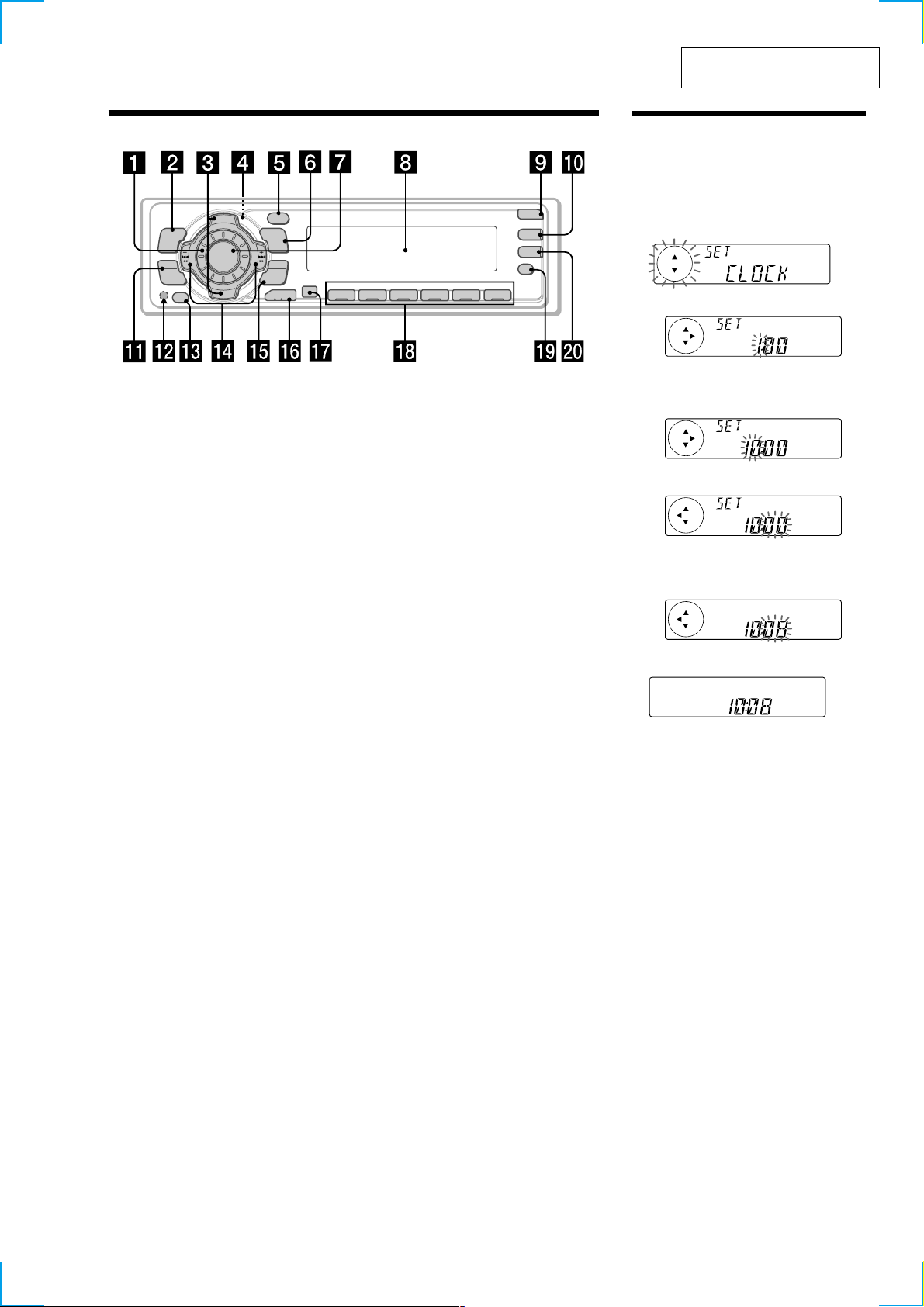
Location of controls
Setting the clock
The clock uses a 24-hour digital indication.
Example: To set the clock to 10:08
1
Press (MENU), then press either side of
(DISC/PRST) repeatedly until “CLOCK”
appears.
1 Press (ENTER).
The hour indication flashes.
2 Press either side of (DISC/PRST) to set
the hour.
3 Press the (+) side of (SEEK/AMS).
The minute indication flashes.
4 Press either side of (DISC/PRST) to set
the minute.
2
Press (ENTER).
The clock starts.
After the clock setting is completed, the
display returns to normal play mode.
Tip
You can set the clock automatically with the RDS
feature (see page 17).
Note
In the initial setting, the clock indication appears
while the unit is turned off.
When the D.INFO mode is set to ON, the time is
always displayed (page 24).
SECTION 1
GENERAL
This section is extracted from
instruction manual.
MENU
SOUND
P
R
S
T
-
-
OFF
Refer to the pages listed for details.
1 Volume control dial 19
2 MENU button 8, 10, 12, 13, 14, 15, 16,
18, 19, 21, 24
3 DISC/PRST +/– (cursor up/down) buttons
8, 10, 12, 13, 14, 15, 16, 18, 19, 20, 21, 24
During CD/MD playback:
Disc change 10, 13
During radio reception:
Preset stations select 16
4
Z (eject) button (located on the front
side of the unit behind the front panel)
9
5 DSPL/PTY (display mode change/
programme type) button 9, 10, 12, 17,
20
6 LIST button 12
List-up 13
7 SOURCE (TUNER/CD/MD) button
8, 9, 10, 13, 15, 16, 19
8 Display window
9 OPEN button 7, 9, 26
q; D-BASS button 25
qa SOUND button 23
qs Reset button (located on the front side
of the unit behind the front panel) 7
qd OFF button* 7, 8, 9
S
C
I
D
SOURCE
D
I
S
C
PTY
+
DSPL
-
P
R
S
T
+
LIST
-
SEEK/AMS
ENTER
–
MODE
REP SHUF
1 2 3 4 56
OPEN
D-BASS
TA
AF
MDX-C6500RV
qf SEEK/AMS –/+ (cursor left/right) buttons
8, 10, 12, 14, 16, 18, 19, 21, 23, 24
Automatic Music Sensor 10, 14
Manual Search 10
Seek 15, 16, 18
qg ENTER button 8, 10, 12, 13, 14, 15, 16,
18, 19, 20, 21, 24
qh MODE button 19
During CD or MD playback:
CD/MD unit select 9, 13
During radio reception:
BAND select 15, 16
qj Receptor for the card remote
commander
qk Number buttons
During radio reception:
Preset number select 15, 16, 18, 19
During CD/MD playback:
(1) REP 11
(2) SHUF 11
ql AF button 17, 18, 19
w; TA button 18, 19
* Warning when installing in a car
without ACC (accessory) position on
the ignition key switch
Be sure to press (OFF) on the unit for two
seconds to turn off the clock display after
turning off the engine.
When you press (OFF) only momentarily,
the clock display does not turn off and this
causes battery wear.
3
Page 4
45678
Page 5
Page 6
Page 7
Page 8
Page 9
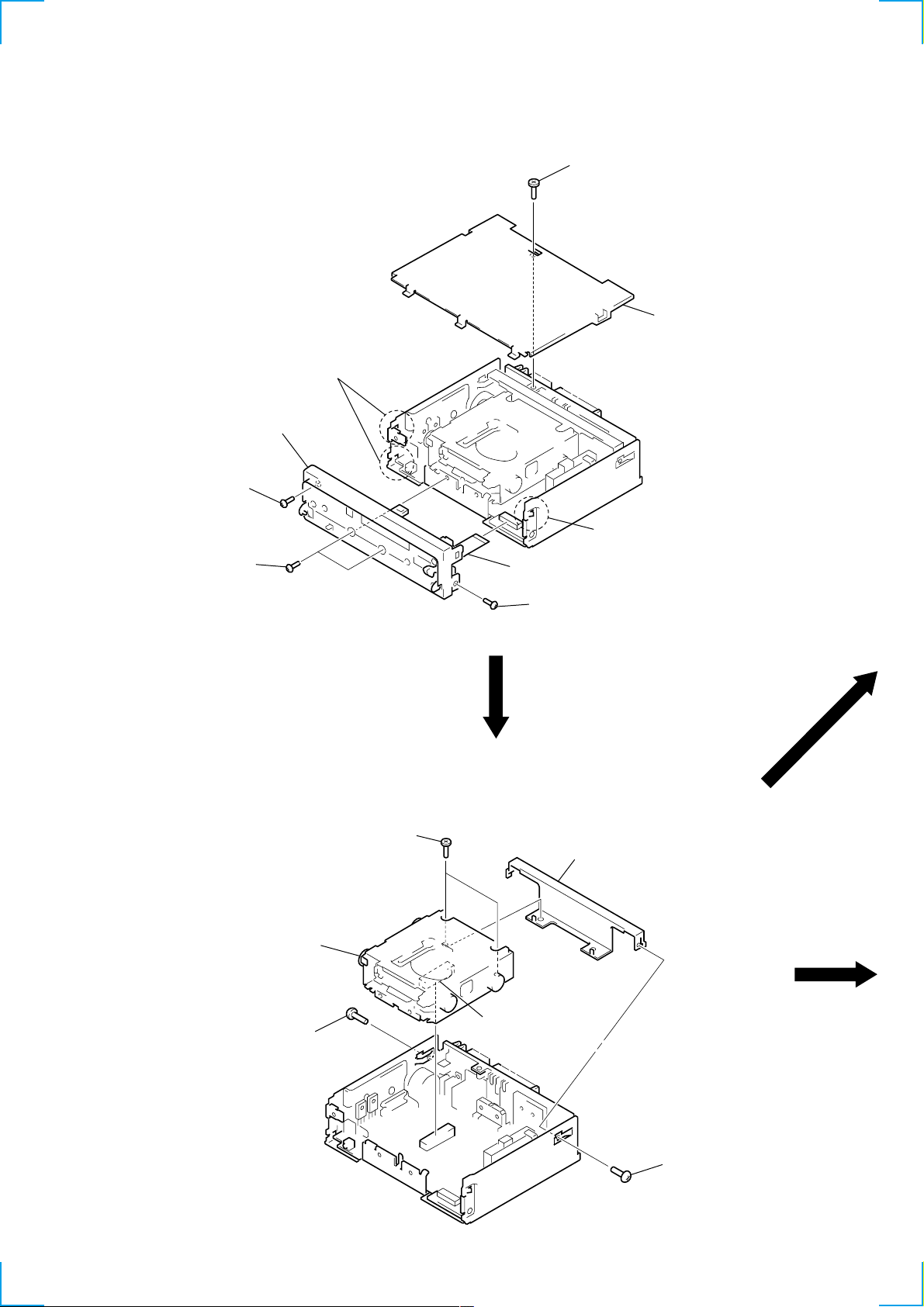
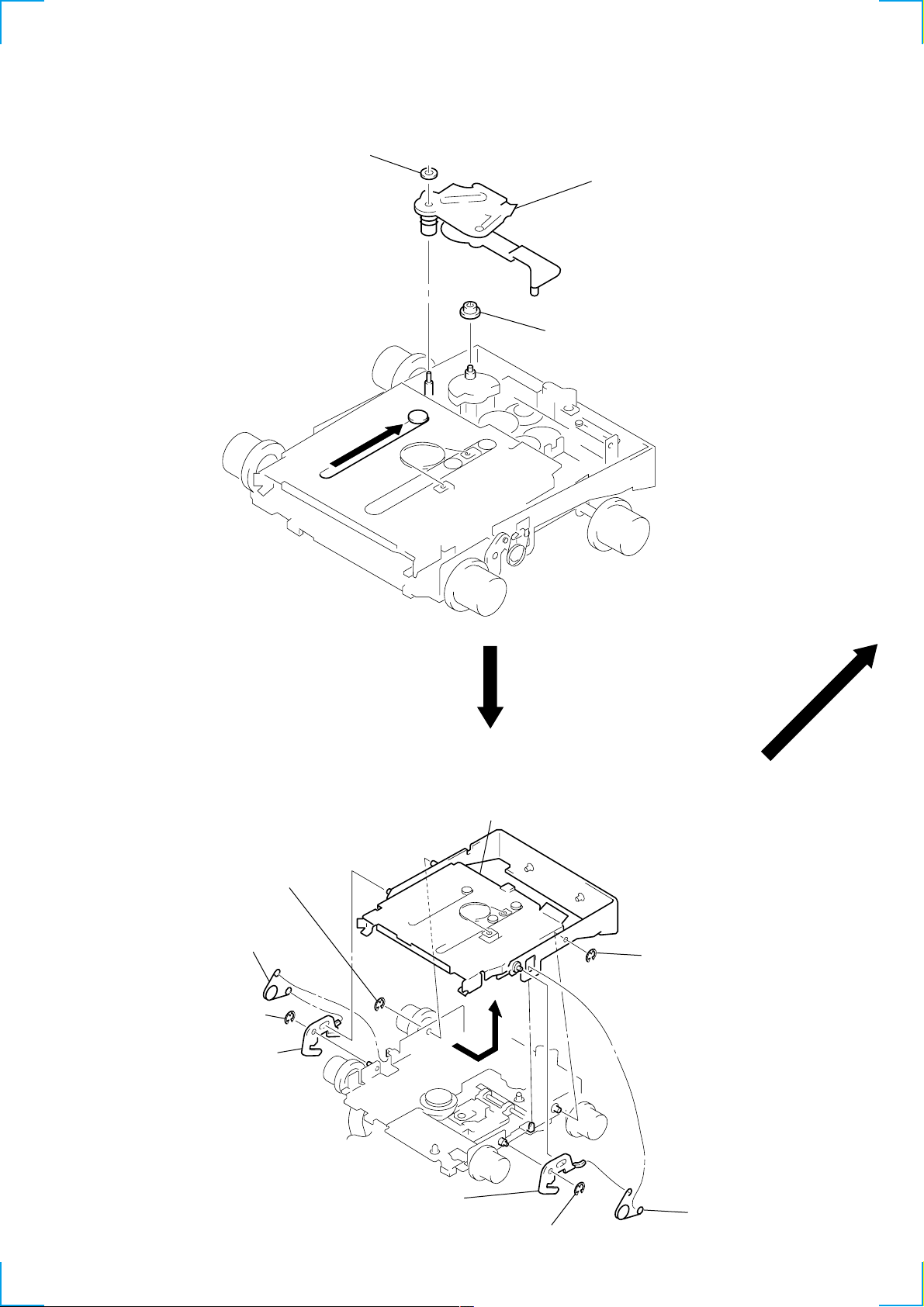
SECTION 2
DISASSEMBLY
Note: Follow the disassembly procedure in the numerical order given.
SUB PANEL ASS’Y
5 sub panel ass’y
3 screw
(PTT2.6 × 8)
3 two screws
(PTT2.6 × 8)
1 screw
(PTT2.6 × 5)
2 cover
4 two claws
4 claw
6 flexible flat cable
(CN500)
3 screw
(PTT2.6 × 8)
MECHANISM DECK (MG-164NZ-138)
2 two screws
(PTT2.6 × 5)
4 mechanism deck
(MG-164NZ-138)
1 screw
(PTT2.6 × 5)
5 bracket (MD)
3 connector
(CN101)
1 screw
(PTT2.6 × 5)
9
Page 10
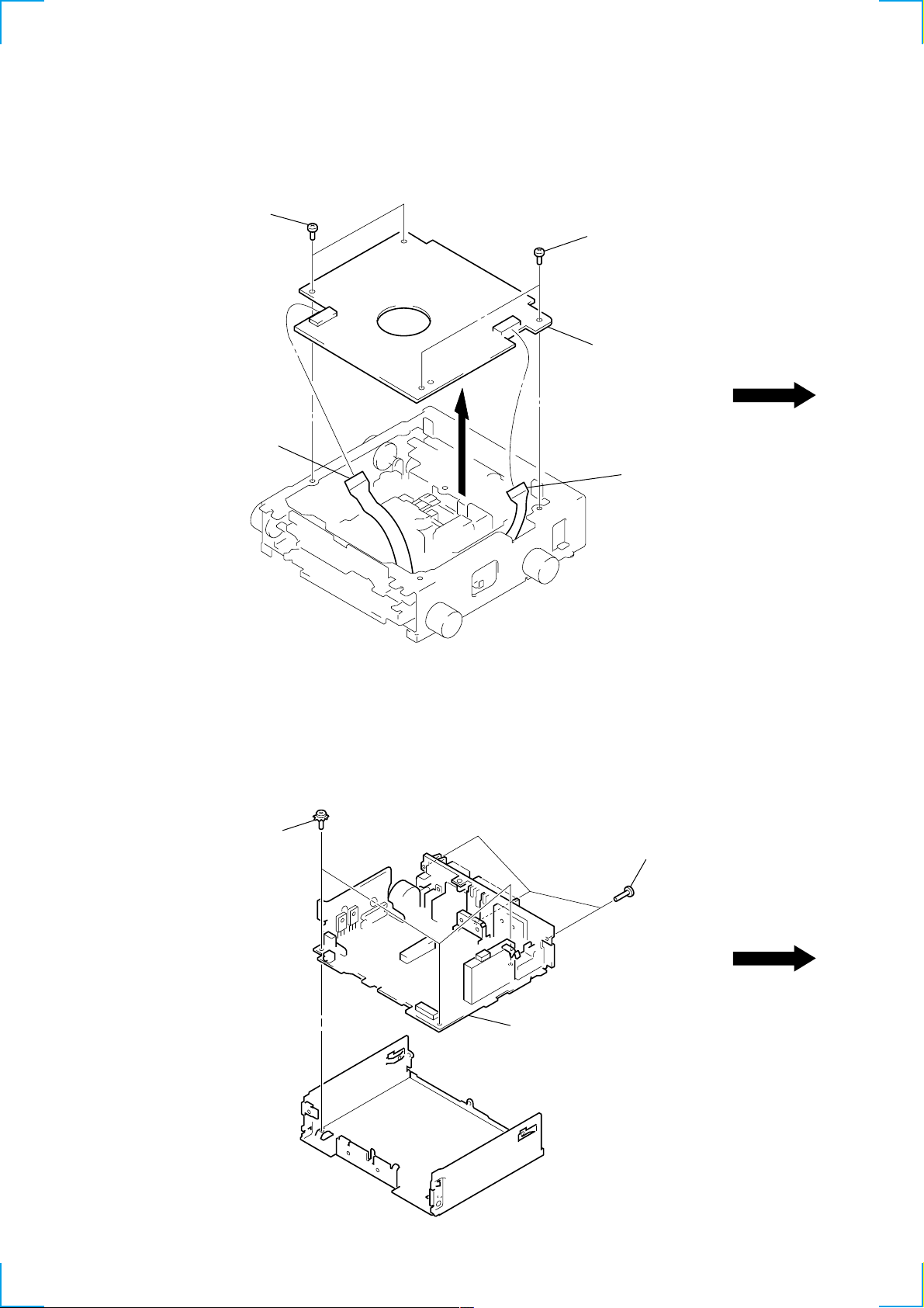
SERVO BOARD
d
1 sensor flexible board
2 two screws
(BVTT2 × 4)
2 two screws
(BVTT2 × 4)
3 servo board
(CN102)
1 flexible boar
(CN103)
MAIN BOARD
1 three ground point
screws
2 three screws
(PTT2.6 × 8)
3 main board
10
Page 11
MD COVER ASS’Y
)
3 MD cover ass’y
cassette holder
1 four screws
(B2 × 3)
shaft (MD cover guide)
HEAT SINK
A
2 Pushing the Cassette Holder in the direction of arrow A with a
screwdriver, etc., disengage the Shaft (MD Cover Guide) from
the slot in the MD Cover Ass’y.
Note: Take care not to scratch the optiocal Pick-up when pushing
the Cassette Holder with a screwdriver. etc.
1 three screws
(PTT2.6 × 8)
3 heat sink
2 two screws
(PTT2.6 × 12)
1 screw
(PTT2.6 × 8
1 two screws
(PTT2.6 × 8)
11
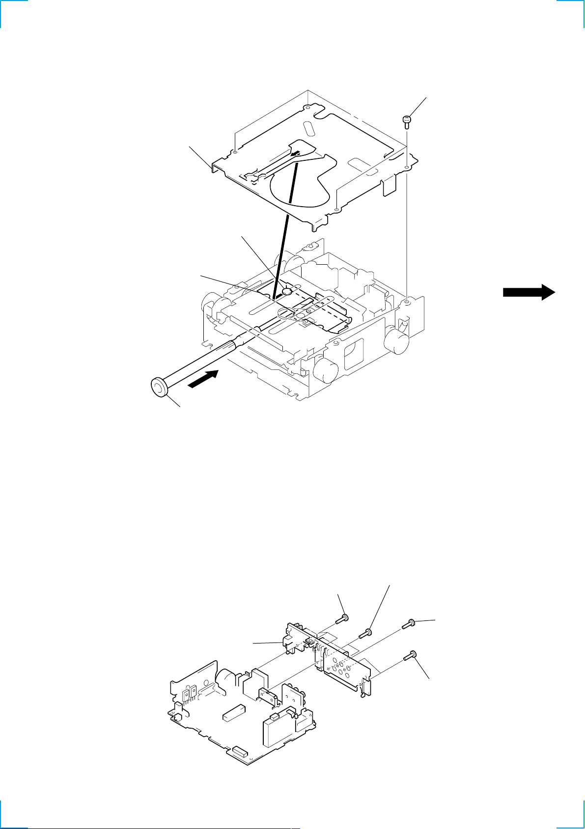
Page 12
FLOAT BLOCK
)
3 Pushing an arrow A part, raise the float block
up ward at the front to release a lock.
float block
A
lever (lock R)
lever (lock L)
1 tension spring (float B)
1 tension spring (float B
2 two tension springs (float F)
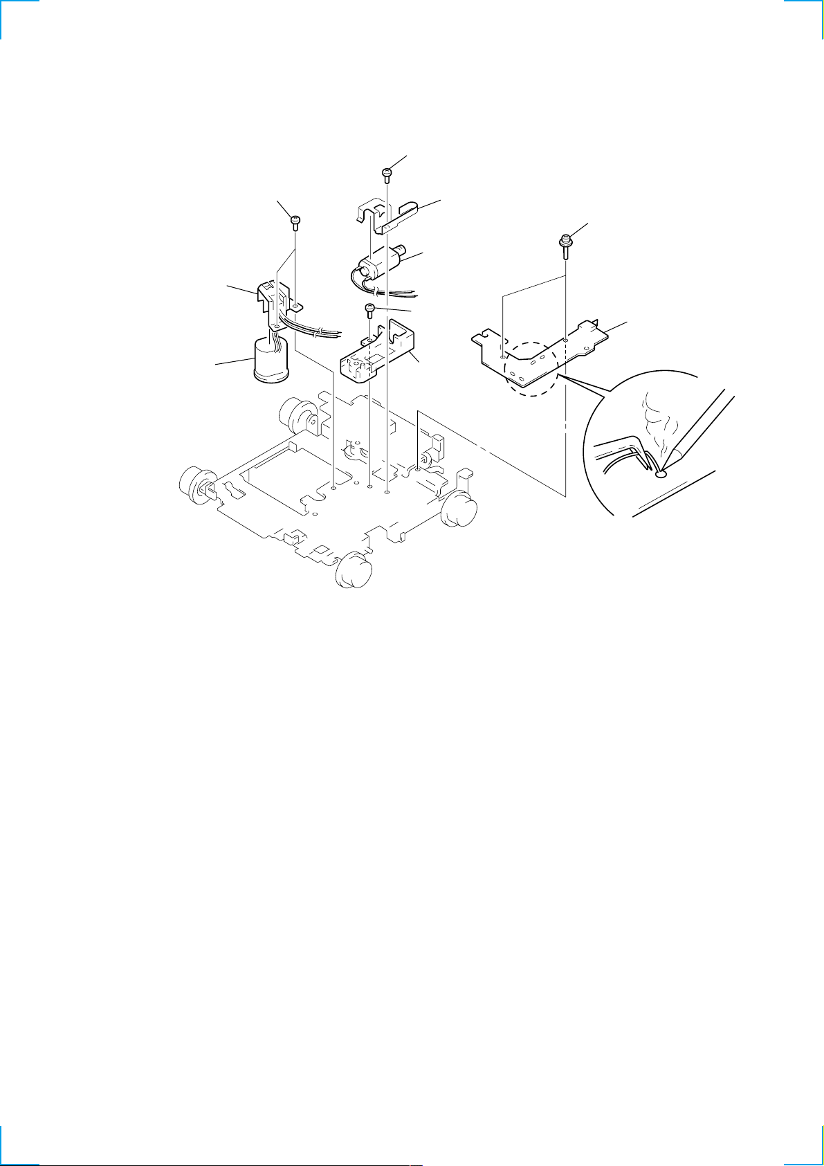
LO MOTOR ASS’Y (LOADING) (M903)
4 Remove the bracket (LO)
in the direction of arrow A.
1 Remove solders of motor (M903)
A
5 LO motor ass’y (loading)
(M903)
2 tension spring (rack)
3 claw
12
bracket (LO)
– bottom view –
Page 13
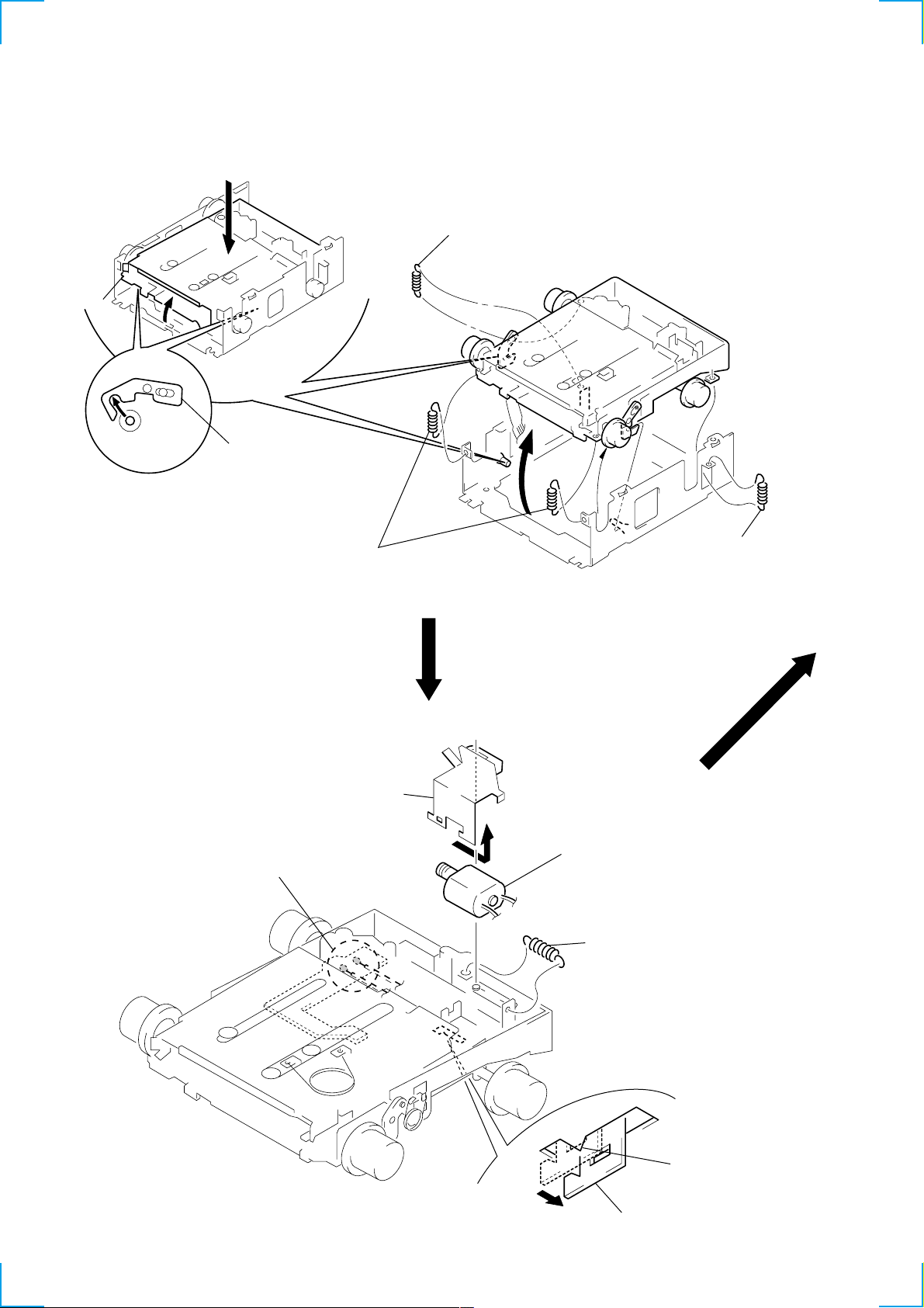
LEVER (LE) ASS’Y
2 stopper washer
2 lever (LE) ass’y
3 roller (gear E)
1
HOLDER ASS’Y
2 type-E stopring 1.5
1 spring (CHKG)
2 type-E stopring 1.5
3 lever (lock R)
4 Remove the holder ass’y in the
direction of the arrow.
2 type-E stopring 1.5
3 lever (lock L)
2 type-E stopring 1.5
1 spring (CHKG)
13
Page 14
CHUCKING ARM ASS’Y
y
holder ass’y
1 Remove the chucking arm ass’y
in the direction of the arrow.
OPTICAL PICK-UP (KMS-241C/J1NP)
7 optical pick-up
(KMS-241C/J1NP)
1 two screws
(K2 × 3)
2 guide shaft (OPT L)
4 screw
(B2 × 3)
6 bearing (SL)
5 feed screw ass’
3 screw
(K2 × 3)
14
Page 15
SL MOTOR ASS’Y (SLED) (M902), SP MOTOR ASS’Y (SPINDLE) (M901)
4 screw
(P1.7 × 1.8)
5 bracket (SL)
9 two screws
(P1.7 × 1.8)
0 bracket (SP)
qa SP motor ass’y
(spindle) (M901)
7 screw
(B2 × 3)
2 two screws
(2 × 8)
3 sensor board
1 Remove solders of motors
(M901, M902)
8 base (SL)
6 SL motor ass’y
(sled) (M902)
15
Page 16

SECTION 3
ELECTRICAL ADJUSTMENTS
TEST MODE
This set have the test mode function.
<Set the Test Mode>
1. Turn ON the regulated po wer supply. (The clock is displayed)
Note: Press the [OFF] button, if the clock is not displayed.
2. Push the preset [4] button.
3. Push the preset [5] button.
4. Press the preset [1] button for more than two seconds.
5. Then the display indicates all lights, the test mode is set.
<Release the Test mode>
1. Push the [OFF] button.
MD SECTION
MD section adjustments are done automatically in this set.
TUNER SECTION
Tuner section adjustments are done automatically in this set.
16
Page 17
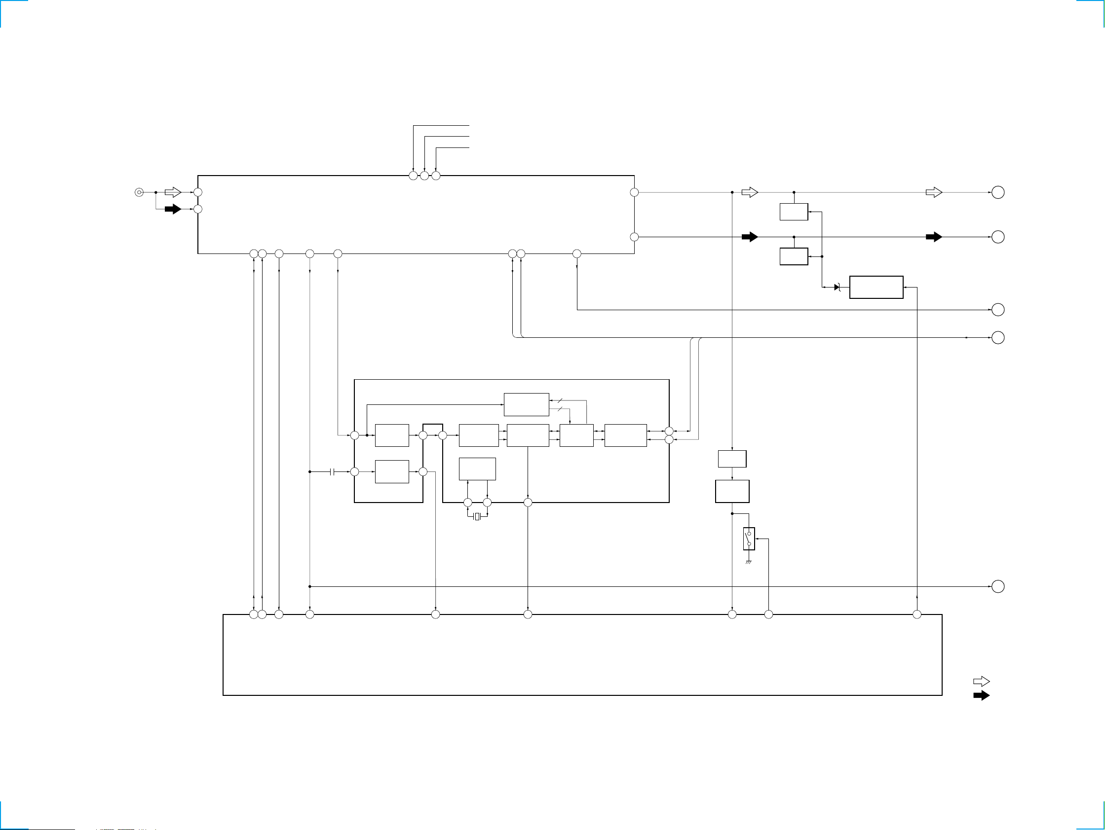
SECTION 4
DIAGRAMS
MDX-C6500RV
4-1. BLOCK DIAGRAM – SERVO Section –
OPTICAL PICK-UP BLOCK
05
F
C B
I J
D A
E
DETECTOR
LASER DIODE
LDPD
(KMS-241C)
2-AXIS
DEVICE
(FOCUS)
(TRACKING)
ILCC
PD
M901
(SPINDLE)
M902
(SLED)
FCS+
FCS–
TRK+
TRK–
I
J
B
A
C
D
E
F
AUTOMATIC
POWER
CONTROL
Q302
FOCUS/TRACKING COIL DRIVE,
SPINDLE/SLED MOTOR DRIVE
6
27
25
21
23
12
10
8
OUT4F
OUT4R
OUT2F
OUT2R
OUT1F
OUT1R
OUT3F
OUT3R
M
M
IC303
I
1
J
2
A
4
B
5
C
6
D
7
E
8
F
9
APC
11
PD
10
IN4R
IN4F
IN2F
IN2R
IN1F
IN1R
IN3F
IN3R
RF AMP
I-V
AMP
I-V
AMP
16PSB
3
4
29
30
19
18
14
15
48 47
MORFO
LD/PD
AMP
SPFD
SPRD
MORFI
RFO
B.P.F.
AT
AMP
12
46
3T
APCREF
IC306
WBL
B.P.F.
ABCD
AMP
WBL3TEQ
V-I
CONVERTER
F0CNT
20
APCREF
83
SFDR
92
SRDR
91
FFDR
88
FRDR
89
TFDR
86
TRDR
85
FOCUS/TRACKING ERROR AMP
AGCI
40
TEMP
ADFM
29 30
FOCUS
ERROR AMP
TRACKING
ERROR AMP
+3.3V
AUTOMATIC
CONTROL
DIGITAL
PROCESS
PWM GENERATOR
RF AMP,
IC302
RF AGC
& EQ
EQ
WBL
PEAK &
BOTTOM
ADIN
COMMAND
SERIAL/
PARALLEL
CONVERTER,
DECODER
XLAT
SCLK
SWDT
1716 18
PEAK HOLD
Q301
+3.3V
13
RECP
POWER
SERVO
SIGNAL
DIGITAL SERVO
SIGNAL PROCESSOR
IC301 (2/2)
RF
AUX
PEAK
BOTM
ADFG
ABCD
FE
TE
SE
ABCD
AUX1
38
33
37
36
32
35
34
26
28
7465647566 63
FE
TE
AUX2
ABCD
ANALOG MUX
A/D CONVERTER
FROM CPU
INTERFACE
AUTO
SEQUENCER
FILTER
73 62
SE
PEAK
XLRF
CKRF
DTRF
100
59
58
61
60
51
52
55
78
79
BOTM
EFMO
FILI
PCO
CLTV
FILO
ASYO
ASYI
COMPA-
RFI
RATOR
ADIP
ADFG
DEMODULATOR/
DECODER
F0CNT
X501
10MHz
80
81
82
PLL
15
TX
EFM/ACIRC
ENCODER/DECODER
SUBCODE
PROCESSOR
SPINDLE
SERVO
SPFD
SPRD
DQSY11SQSY14XINT
XRST
94 93
10
12
59 62 55 54 52 45 51 64 26 27 28 29
MD-RST
31
EXTAL
XTAL
32
7 6
LOADING
MOTOR DRIVE
IC305
M903
(LOADING)
5 4
RIN FIN
OUT1 OUT2
1 7
SHOCK PROOF
MEMORY CONTROLLER
51331
LEVEL SHIFT
IC502
61242
SQSY
CC-XINT
EJECT
LOAD
M
ATRAC
CPU
INTERFACE
SENS
SRDT
SWDT
9 8 5 6 7
SWDT
SENS
MD-SI
MD-SO
MD MECHANISM CONTROLLER
ON: When the disc loading start
and the disc eject completion.
IC301 (1/2)
SAMPLING
RATE
CONVERTER
DIGITAL
AUDIO
ENCODER/DECODER
INTERFACE
D-RAM
INTERNAL BUS
MONITOR
CONTROL
SCLK
XLAT
MNT0
1 2 3 4
13
LEVEL SHIFT
IC503
12
FOK
SCLK
XLAT
MNT0
MD-LAT
MD-CKO
IC501 (1/2)
C-SW
63
LOADING START/
EJECT END
ADDT
23
DIN
21
DOUT
22
DADT
24
MNT1
MNT2
MNT3
135
246
SHOCK
XBUSY
SLOCK
MNT1
MNT2
MNT3
LOADING
END
ON: When completion of
the disc loading.
DIGITAL SIGNAL PROCESSOR,
EFM/ACIRC ENCODER/DECODER,
SHOCK PROOF MEMORY CONTROLLER,
ATRAC ENCODER/DECODER, 2M BIT D-RAM
IC301 (1/2)
BCK
LRCK
FS256
2526 27
LRCK
XBCK
FS256
CLOCK
GENERATOR
RESET
TH501
39
TEMP
E-SW
11 56
OSCI
OSCO
XOE
XWE
XRAS
XCAS
EMPHASIS
66
DEEMP
(LIMIT)
ON: When the optical pick-up is
inner position.
16
17
D0 – D3A00 – A09
47, 46, 48, 49
32 – 29, 34 – 38, 43
41 22
45 3
44 4
42 23
LOCK
A-MUTE
LIMIT-IN
• SIGNAL PATH
DADT, BCK, LRCK, FS256
512FS OSC
IC304
1, 2, 24, 25
9 – 12, 14 – 18, 5
OE
WE
RAS
CAS
RESET, EMPHASIS
21
67
D0 – D3
A0 – A9
D-RAM
IC307
: MD PLAY
X301
22.5792MHz
LOCK
MD-ATT
(Page 19)
A
(Page 19)
B
C
(Page 19)
D
(Page 19)
1717
Page 18
MDX-C6500RV
4-2. BLOCK DIAGRAM – TUNER Section –
FM/AM TUNER UNIT
2
1
ANT-FM
ANT-AM
TU1
SDA (E2PROM)
SCL (E2PROM)
17
18
FM-AGC
4
S-METER
14
J1
(FM/AM ANTENNA)
RDS-DET
9
11
5
VCC (8.5V)
VDD E2P (5V)
16
VDD (5V)
BU B+
TUNER +8.7V
TUNER +5.6V
SDA (I2CBUS)
SCL (I2CBUS)
12 13
19
IF-AM
MPX
AM-DET
10
MUTING
Q111
8
MUTING
Q121
MUTING
CONTROL SWITCH
D131
Q131
MPX
AM
IF-AM
E
F
G
(Page 19)
(Page 19)
(Page 19)
DATA
CLOCK
DATA
CLOCK
RDS DECODER
IC51
PATH
OUT
SC
18
MPTH
2
CIN
CLOCKED
19
COMPARATOR
OSCILLATOR
& CLOCK
OSCI
OSCO
4
5
X51
4.332MHz
52
MPX
LVIN
57 kHz
BAND-PASS
FILTER
MULTI
DETECTOR
16
20
9
10
51
53
SIGNAL
QUALITY
DECODER
RDS/RDBS
DEMODULATOR
& DECODER
DAVN
8
64
5
4
INTERFACE
REGISTER
IIC BUS
SLAVE
TRANSCEIVER
SDA
SCL
9
10
BUFFER
Q1
BAND-PASS
FILTER
IC90
Q90
NOISE DET
DISCHARGE
SWITCH
50
32
56
DATA, CLOCK
S-METER
I
H
(Page 19)
(Page 19)
E2P SIO
E2P CKO
FMAGC
VSM
MPTH
MASTER CONTROLLER
IC501 (1/3)
DAVN
QUALITY
NS MASK
TUNATT
• SIGNAL PATH
: FM
05
: MW/LW
1818
Page 19
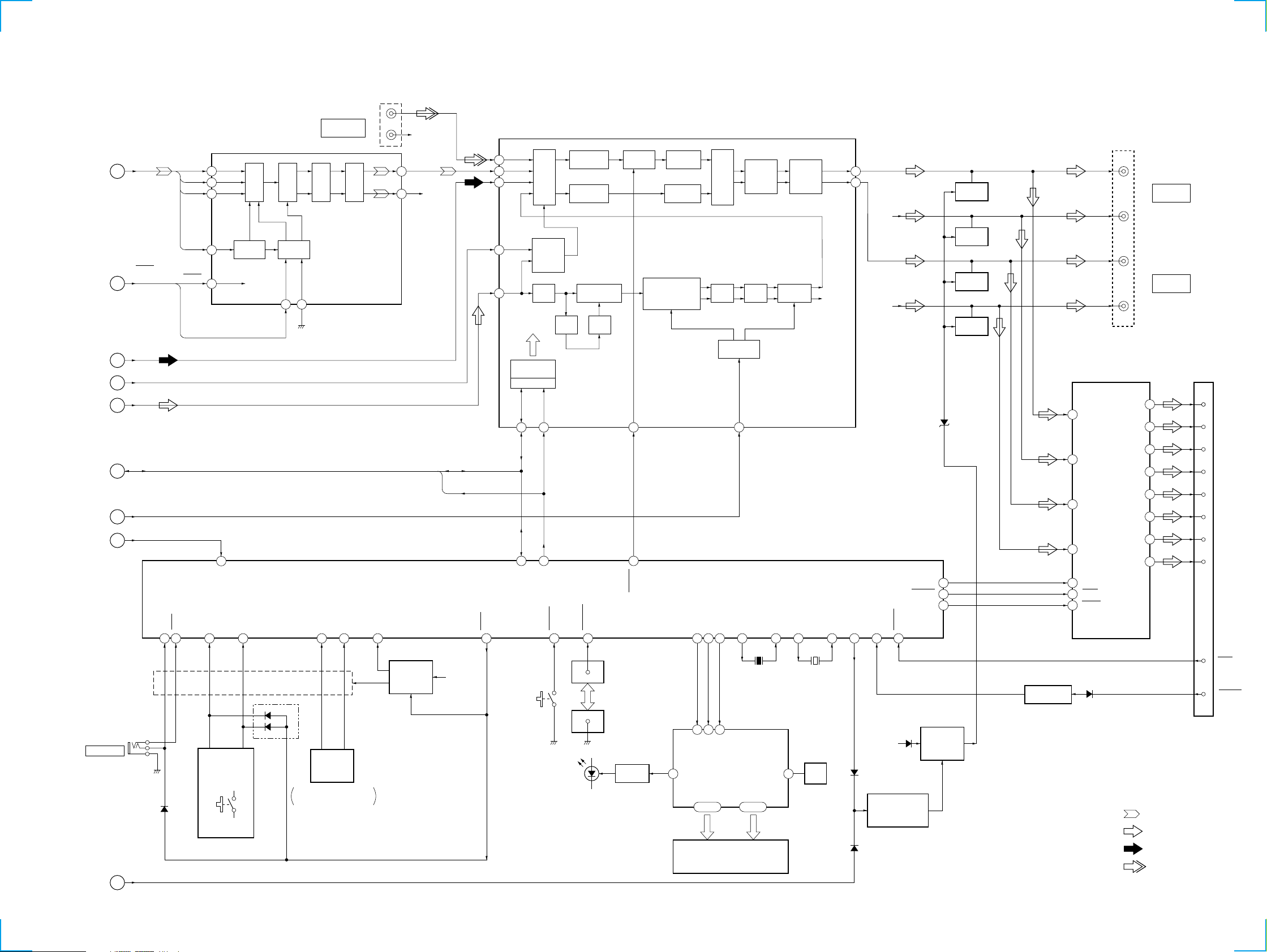
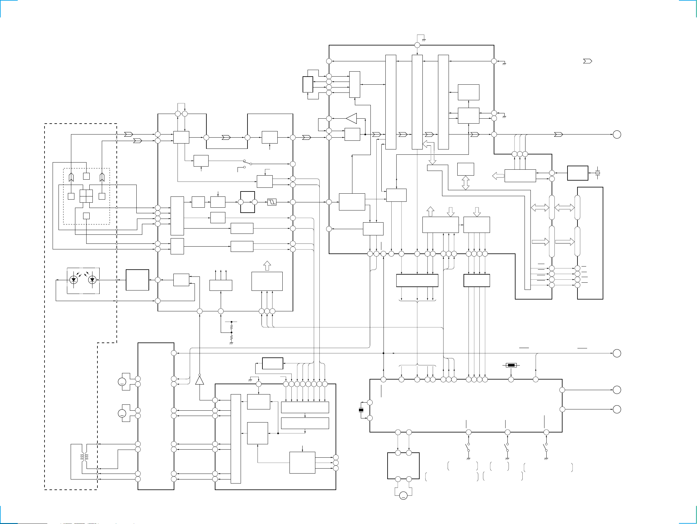
4-3. BLOCK DIAGRAM – MAIN Section –
MDX-C6500RV
(Page 17)
(Page 17)
(Page 18)
(Page 18)
(Page 18)
(Page 18)
(Page 18)
(Page 17)
CNJ151 (1/2)
DM0
NOISE
SHAPER
AUDIO IN
DADT,
BCK,
LRCK,
FS256
A
LRCK
FS256
RESET,
EMPHASIS
B
AM
F
IF-AM
G
MPX
E
I
S-METER
H
LOCK
C
RESET
EMPHASIS
DATA, CLOCK
DATADADT
5
BCKBCK
6
4
1
15
84
LRCK
XTI
RSTB
LOCKIN
INPUT
CLK
CONTROL
INTERFACE
CONTROL
FILTER
DIGITAL
MODE
DM1
17 16
(L)
BUS
(R)
VOUTL
D/A
VOUTR
COMVERTER
DIGITAL FILTER,
D/A CONVERTER
IC101
R-CH
12
9
R-CH
MASTER CONTROLLER
IC501 (2/3)
INPUT SELECT,
ELECTRICAL VOLUME, FM MPX
3
1
11
12
13
DATA
CLOCK
FD1L
SEL
AM
AMIF
MPX
IC151
BLANKER
L.P.F.
DIGITAL
CONTROL
IIC BUS
SDA
20
70 71
I2C SIO
INPUT
MULTIPLEXER
AM/FM
NOISE
SCL
21
I2C CKO
PLL
LOUDNESS/
VOLUME
PILOT
CANCELATION
PILOT
DET
SOFT
MUTE
DEMODULATOR
+STEREO ADJUST
+STEREO BLEND
SM
18
57
VOLATT
TONE
CONTROL
LOUDNESSMUTE
MONO
FADER
OUTPUT
SELECTOR
L.P.F. S & H HIGH-CUT
D/A
CONVERTER
LEVEL
14
MIXER
OUTLF
OUTLR
R-CH
CNJ151 (2/2)
FL+
FL–
FR+
FR–
RL+
RL–
RR+
RR–
(L)
(R)
(L)
(R)
AUDIO OUT
FRONT
AUDIO OUT
REAR
(POWER CONNECTOR)
5
3
21
23
9
7
17
19
CN601 (1/2)
1
9
4
12
2
10
3
11
FRONT L (+)
FRONT L (–)
FRONT R (+)
FRONT R (–)
REAR L (+)
REAR L (–)
REAR R (+)
REAR R (–)
30
29
R-CH
R-CH
D621
BEEP
AMPATT
AMPON
MUTING
Q171
MUTING
Q271
MUTING
Q181
MUTING
Q281
POWER AMP
IC611
12
FL-IN
14
FR-IN
RL-IN
11
15
RR-IN
16
60
59
16
AUX IN
MUTE
22
4
STNBY
J501
REMOTE IN
(Page 17)
05
RCIN1
RCIN0
48 46 47 36 37 76 6785 12 587473929315141335 79 81
D653
KEYIN0
LSW810,
LSW901 – 917,
S901 – 904
KEYIN1
D501
VOLUME/BASS/TREBLE/
BALANCE/FADER CONTROL
REIN0
ROTARY
ENCODER
RE901
REIN1
KEYACK
KEY ACTIVE
SWITCH
Q651, 652
U-COM +5V
AD-ON
SW504
(NOSE DETECT)
NOSESW
LED910 – 915
(LCD BACK LIGHT)
DOORSW
14
MAIN BODY SIDE
1
FRONT PANEL SIDE
CN500
CN901
LED DRIVE
Q903
LCDSO
LCDCKO
LCDCE
X1
X0
X501
3.68MHz
6263
64
DI
CL
SE
LIQUID CRYSTAL
DIMMER
S04
DISPLAY DRIVER
IC901
–
S51 COM1
–
4
51
OSC
–
COM4
–
52
55
3 60
X1A
X502
32.768kHz
OSC
C953, R957
X0A
ATT
TELATT
BACK-UP B+
D502
CONTROL SWITCH
MUTING
Q622
TEST IN
D622
BATTERY OFF
MUTE DRIVER
Q621
LEVEL SHIFT
Q571
D571
• SIGNAL PATH
: MD PLAY
15
TEST
13
TEL-ATT
: FM
LCD901
LIQUID CRYSTAL DISPLAY
MD-ATT
D
D302
: MW/LW
: BUS AUDIO IN
1919
Page 20
MDX-C6500RV
4-4. BLOCK DIAGRAM – BUS CONTROL/POWER SUPPLY Section –
CN701
BUS CONTROL IN
(FOR SONY BUS)
SIRCS
RESET
DATA
CLK
BUS ON
BATT
BACK-UP B+
3
2
5
4
6
7
BUS ON SWITCH
Q705
TH701
D708
BU B+
2
6
4
1
3
D702
D701
SIRCS BUFFER
Q704
RESET SIGNAL
GENERATOR
IC652
SONY BUS INTERFACE
IC701
RST
RESET
SWITCH
DATA
CLK
BUS ON
OUT
BATT
BATTERY
DETECT
Q701
BUS ON
SWITCH
BATTERY
SWITCH
DATA IN
DATA OUT
RST
CLK IN
BUS
ON IN
BU IN
REMOTE CONTROL
RECEIVER
IC951
SW503
RESET
13
9
8
11
12
10
D301
MASTER CONTROLLER
IC501 (3/3)
24
SIRCS
RSTX
90
86
HSTX
11
SYSRST
UNISO
18
17
UNISI
19
UNICKO
20
UNICKI
3
BUSON
BUIN
77
PW ON
TUNON
ILLON
ACC IN
CN601 (2/2)
BACK-UP B+
POWER AMP
(IC611) B+
(POWER CONNECTOR)
6
5
FU601
16
7
ANT-R
AMP-R
+B
ACC
D673
D674
6
AMP+B
8
ANT+B
REGULATOR
TUNER +8.7V
TUNER +5.6V
RDS DECODER
(IC51) B+
COM +8V
(AUDIO CIRCUIT B+)
BU B+
PULL UP +5V
U-COM +5V
120
1
7
82
REGULATOR
CONTROL SWITCH
Q633
D677
LED901 – 904,
LSW901 – 917
D2
D1
D676
LCD DRIVER
(IC901) B+
ACCESSORY CHECK
11
10
9
5
LCD B+
TU8.7V
TU5.6V
COM8V
BU+B
Q661
IC671
STB
4
VCC
8.7VON SW
5.6VON SW
23
REGULATOR
7
Q631
D662
29
DOORIND
LO +12V
MD MECHANISM CONTROLLER
IC501 (2/2)
MDMON
65MD-ON
REGULATOR
10
CONTROL SWITCH
Q363
REGULATOR
CONTROL SWITCH
Q250
60
BU-IN
BUS-ON
61
30
RESET
UNISI
49
48
UNICKIO
LEVEL SHIFT
Q706
05
50
46
UNISO
LINKOFF
LOADING MOTOR
DRIVER (IC305) B+
+3.3V
LED810
(MD DISC SLOT)
LSW810
Z
VCC
+3.3V
REGULATOR
IC401, Q401
LED810,
LSW810
B+ SWITCH
Q402, 403
DRIVER +5V
MOTOR/COIL DRIVER
(IC303) B+
REGULATOR
Q551
+12V
REGULATOR
Q361
+5V
REGULATOR
Q362
2020
Page 21

MDX-C6500RV
• Circuit Boards Location
SUB board
KEY board
SENSOR board
SERVO board
4-5. NOTE FOR PRINTED WIRING BOARDS AND SCHEMATIC DIAGRAMS
Note on Printed Wiring Board:
• X : parts extracted from the component side.
• Y : parts extracted from the conductor side.
z
•
•
: Through hole.
f
: internal component.
• b : Pattern from the side which enables seeing.
(The other layers' patterns are not indicated.)
Caution:
Pattern face side: Parts on t he patte rn face side seen from
(Conductor Side) the pattern face are indicated.
Parts face side: Parts on the parts face side seen from
(Component Side) the parts face are indicated.
Note on Schematic Diagram:
• All capacitors are in µF unless otherwise noted. pF: µµF
50 WV or less are not indicated except for electrolytics
and tantalums.
• All resistors are in Ω and 1/
specified.
4
• % : indicates tolerance.
f
•
: internal component.
• C : panel designation.
Note: The components identified by mark 0 or dotted line
with mark 0 are critical for safety.
Replace only with part number specified.
• U : B+ Line.
• Pow er voltage is dc 14.4V and fed with regulated dc po wer
supply from ACC and BATT cords.
• V oltages are taken with a VOM (Input impedance 10 MΩ).
Voltage variations may be noted due to normal production tolerances.
• Waveforms are taken with a oscilloscope.
Voltage variations may be noted due to normal production tolerances.
• Circled numbers refer to waveforms.
• Signal path.
E : MD PLAY
F : FM
f : MW/LW
L : BUS AUDIO IN
W or less unless otherwise
MAIN board
2121
Page 22

MDX-C6500RV
4-6. PRINTED WIRING BOARDS – SERVO Board (Component Side)/SENSOR Board – • See page 21 for Circuit Boards Location.
• Semiconductor
A
B
C
D
Location
Ref. No. Location
D401 A-12
D501 D-11
IC101 B-9
IC301 D-7
IC302 I-9
IC303 F-7
IC304 C-8
IC305 B-13
IC306 E-6
IC401 A-12
IC501 G-13
IC502 D-10
IC503 E-10
Q301 E-5
Q302 I-8
Q401 B-11
SENSOR BOARD
(COMPONENT SIDE)
E
SENSOR BOARD
(CONDUCTOR SIDE)
F
G
1
(LIMIT)
2 3 4 5 6 7 8 9 10 11 12 13 14
M902
(SLED)
(LOADING END)
M903
(LOADING)
RED
MM
BLK
11
1
RED
MM
BLK
RED
1-676-656-
BLK
MM
11
(11)
M902
(SPINDLE)
SERVO BOARD
(COMPONENT SIDE)
(CHASSIS)
R320
C308
R325
C310
R328
C311
Q301
R324
R327
C306
R319
C305
R318
50 26
51
C304
IC301
R317
FB301
C103 C105
20 11
IC101
R316
R311
R312
25
FB302
8
C341R354C340
5
110
C104
R102
8
L101
+
C109
C108
L102
+
C106
C107
7
R404
C402 R405
E
C
Q401
5
B
8
C403 C406
29 30
IC304
1
4
X301
IC502
IC401
4
1
D401
CN101
K
A
C352
1
C11
8
IC305
4
11
CN103
5
(CHASSIS)
SENSOR FLEXIBLE
R308
75
76
BCE
R329
R330
C315
L304
C338 C314C339
32 17
C348
5
IC306
1
R331
4
R353
R352
C343
3
C342
L303
1
100
R351
C337
C349
R307
R306
R305
R304
R303
R302
R301
14
8
IC503
14
IC303
116
L305
L306
C336
C335
1
7
1
D501
K
A
12
80
1
R501
R502
R503
R531
R538
IC501
1
1-654-693-
R525
R524
R523
R530
R522
65
R518
R537
R536
64
BOARD
11
R517
A
MAIN BOARD
CN301
(Page
27)
R535
R505
R527
R528
R526
R529
R539
C516
R504
C501
X501
R516
24
25
R532
R507
R506
41
40
R511
(CHASSIS)
11
1-675-655-
(11)
C334
+
C318
R355
CN102
1
C331
R356
+
C319
20
C320
R337
C321
R348
C322
Q302
BCE
R349
R357
C329
1
IC302
12
R341
R350
C328
36
25
R339
R345
R343
R338
C330
C327
C326
C325
R347
C324
R344
R342
R346
C347
L302
+
C346
3748
2413
R340R336
H
(CHASSIS)
OPTICAL
PICK-UP
BLOCK
(KMS-241C)
I
LOADING START
EJECT END
05
1-676-656-
11
(11)
2222
Page 23

4-7. PRINTED WIRING BOARD – SERVO Board (Conductor Side) – • See page 21 for Circuit Boards Location.
MDX-C6500RV
1
A
SERVO BOARD
(CONDUCTOR SIDE)
B
C
D
2 3 4 5 6 7 89
• Semiconductor
C511
L301
+
C102
C202
+
C344
+
C345
C359
C353
C302
C362
+
C361
15913
IC307
C307
26221814
C309
C358
C301
C317
C356
C357
L501
C510
Q402
R539
BCE
Q403
R402
R403
C101
C201
R101
R201
R104
R202
R401
B
E
C
Location
Ref. No. Location
IC307 C-8
Q402 B-4
Q403 B-4
E
C515
F
C514
C513
R521R520
G
R519
H
R512
R534
R533
C503
R510
TH501
C504
C506
C505
+
R542
R540
RB503
C512
R332
R334
R333
R335
RB301RB302
C333
C316
+
C351
C350
I
05
1-675-655-
2323
11
(11)
Page 24

MDX-C6500RV
4-8. SCHEMATIC DIAGRAM – SERVO Board (1/2) – • See page 31 for Waveforms. • See page 36 for IC Block Diagrams.
• Voltages and waveforms are dc with respect to ground
under no-signal conditions.
no mark : MD PLAY
: Impossible to measure
∗
The components identified by mark 0 or dotted
line with mark 0 are critical for safety.
Replace only with part number specified.
2424
Page 25

4-9. SCHEMATIC DIAGRAM – SERVO Board (2/2) – • See page 31 for Waveforms. • See page 36 for IC Block Diagrams.
MDX-C6500RV
(Page
29)
• Voltages and waveforms are dc with respect to ground
under no-signal conditions.
no mark : MD PLAY
: Impossible to measure
∗
2525
Page 26

MDX-C6500RV
4-10. PRINTED WIRING BOARD – MAIN Board (Component Side) – • See page 21 for Circuit Boards Location.
• Semiconductor
Location
Ref. No. Location
D1 E-9
D301 G-5
D501 I-7
D502 H-7
D551 J-13
D552 K-13
D553 K-13
D554 J-12
D555 K-13
D556 J-12
D557 K-13
D558 J-12
D559 K-13
D560 J-12
D571 B-5
D603 B-4
D605 B-5
D611 B-7
D612 B-7
D613 C-7
D614 C-7
D615 C-7
D616 C-7
D617 C-6
D618 C-6
D622 D-9
D624 C-9
D653 I-7
D661 D-5
D662 D-5
D673 C-5
D674 C-5
D701 E-5
D702 C-4
D703 B-3
D704 B-2
D705 B-2
D706 B-2
D708 G-7
D710 D-4
IC51 I-12
IC90 G-11
IC151 D-10
IC501 I-5
IC652 J-3
IC701 C-3
Q1 G-11
Q111 E-12
Q131 F-12
Q171 B-11
Q181 B-11
Q250 H-2
Q271 C-11
Q281 C-11
Q363 I-3
Q551 J-6
Q571 D-5
Q621 C-10
Q622 C-9
Q633 J-2
Q651 I-8
Q652 I-8
Q661 D-5
Q701 D-5
Q704 G-7
Q705 C-4
Q706 D-4
2626
Page 27

4-11. PRINTED WIRING BOARD – MAIN Board (Conductor Side) – • See page 21 for Circuit Boards Location.
RL–
FL–
FR–
FL+
FR+
RL+
RL–
FL–
9
1 2 3 4 5 6 7 8
FL+
RR+
ATT
FR–
RR–
RL–
10 11 12 13 14 15 16
FR+
RL+
RR+
AMP REM
ACC
ANT REM
MDX-C6500RV
5 4
BATT
GND
BATT
ACC
GND
ANT REM
6
8
2 13
(FRONT VIEW)
7
• Semiconductor
Location
Ref. No. Location
D2 E-7
D90 H-11
D91 H-11
D92 G-11
D131 F-12
D302 G-7
D361 I-2
D362 G-2
D561 K-11
D562 K-11
D563 K-13
D564 K-12
D601 C-3
D602 B-4
D604 A-5
D621 B-10
D631 J-2
D671 C-5
D672 C-5
D675 I-4
D676 I-4
D677 I-4
D709 G-5
IC611 A-7
IC671 F-1
Q90 G-11
Q121 E-12
Q361 H-1
Q362 G-1
Q631 J-2
(Page 32)
(Page 22)
2727
Page 28

MDX-C6500RV
4-12. SCHEMATIC DIAGRAM – MAIN Board (1/3) – • See page 31 for Waveforms. • See page 36 for IC Block Diagrams.
• Voltages and waveforms are dc with respect to ground
under no-signal (detuned) conditions.
no mark : FM
( ) : MW
[]: LW
(Page
30)
(Page 29)
2828
Page 29

4-13. SCHEMATIC DIAGRAM – MAIN Board (2/3) – • See page 31 for Waveforms.
MDX-C6500RV
(Page 28)
(Page
25)
(Page
30)
• Voltages and waveforms are dc with respect to ground
under no-signal (detuned) conditions.
no mark : FM
( ) : MW
[]: LW
〈〈 〉〉 : MD PLAY
2929
: Impossible to measure
∗
Page 30

MDX-C6500RV
4-14. SCHEMATIC DIAGRAM – MAIN Board (3/3) – • See page 36 for IC Block Diagrams.
(Page
28)
(Page
33)
(Page
29)
• Voltages are dc with respect to ground under no-signal
(detuned) conditions.
no mark : FM
〈〈 〉〉 : MD PLAY
3030
Page 31

• Waveforms
– SERVO Board –
– MAIN Board –
MDX-C6500RV
– KEY Board –
1 IC101 1 (XTI) (MD Play Mode)
4.4 Vp-p
88 ns
2 IC101 4 (LRCK) (MD Play Mode)
3.8 Vp-p
22.7 µs
3 IC101 6 (BCK) (MD Play Mode)
6 IC301 wh (XBCK) (MD Play Mode)
4.6 Vp-p
354 ns
7 IC301 wj (FS256) (MD Play Mode)
4.4 Vp-p
88 ns
8 IC301 tg (RFI), IC302 ek (RF)
(MD Play Mode)
qa IC302 1, 2, r;, rh (I, J, AGCI, RFO)
(MD Play Mode)
Apporx.
0.6 Vp-p
qs IC304 1, 2 (MD Play Mode)
4.1 Vp-p
44.3 ns
qd IC304 3 (MD Play Mode)
1 IC51 4 (OSCO)
231 ns
2 IC501 ud (X1A)
30.5 µs
3 IC501 od (X1)
5 Vp-p
5.4 Vp-p
1 IC901 y; (OSC)
2.6 Vp-p
26.4 µs
3.4 Vp-p
354 ns
4 IC301 qh (OSCI) (MD Play Mode)
4.6 Vp-p
44.3 ns
5 IC301 wg (LRCK) (MD Play Mode)
4.4 Vp-p
9 IC301 yg (FE), IC302 ef (FE)
(MD Play Mode)
0 IC301 uf (TE), IC302 wh (TE)
(MD Play Mode)
Apporx.
1.5 Vp-p
Approx.
0.5 Vp-p
Approx.
2 Vp-p
44.3 ns
qf IC304 7 (MD Play Mode)
44.3 ns
qg IC501 ea (EXTAL)
3.4 Vp-p
4.4 Vp-p
3.7 Vp-p
5.6 Vp-p
272 ns
22.7 µs
101 ns
3131
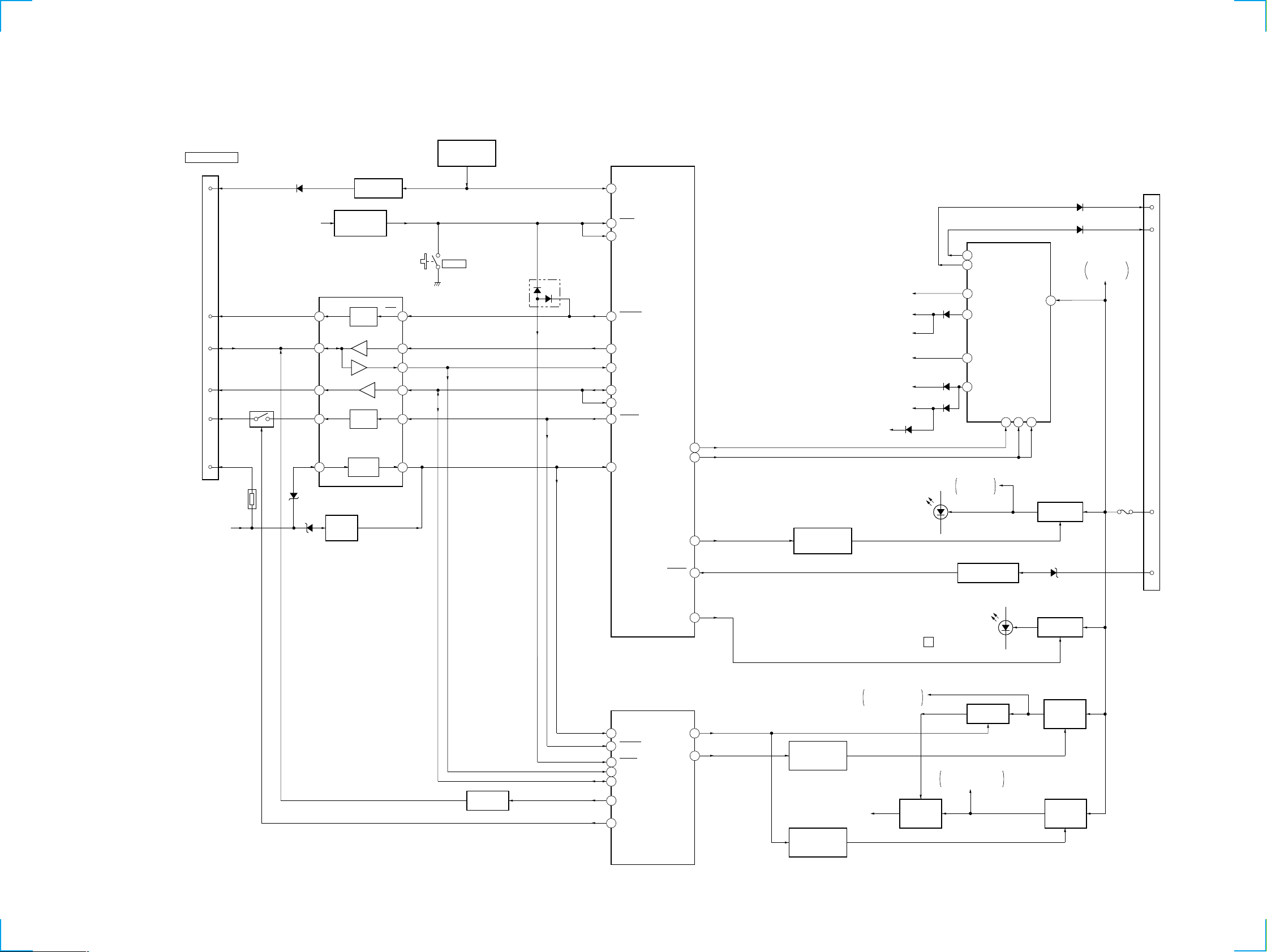
Page 32

MDX-C6500RV
4-15. PRINTED WIRING BOARD – SUB Board –• See page 21 for Circuit Boards Location.
(Page 27)
(Page 34)
3232
Page 33

4-16. SCHEMATIC DIAGRAM – SUB Board –
(Page 30)
MDX-C6500RV
3333
Page 34

MDX-C6500RV
4-17. PRINTED WIRING BOARD – KEY Board –• See page 21 for Circuit Boards Location.
• Semiconductor
Location
(Component Side)
Ref. No. Location
IC951 C-5
LED901 A-2
LED902 C-2
LED903 C-3
LED904 A-3
LED910 B-12
LED911 B-12
LED912 A-12
LED913 A-5
LED914 B-5
LED915 B-5
• Semiconductor
Location
(Conductor Side)
Ref. No. Location
D901 A-11
D902 B-10
D903 B-10
D904 B-10
D951 C-4
D952 B-6
IC901 B-8
Q903 A-5
BCE
Q903
(Page 32)
3434
Page 35

4-18. SCHEMATIC DIAGRAM – KEY Board –• See page 31 for Waveforms.
(Page
33)
MDX-C6500RV
• Voltages and waveforms are dc with respect to ground
under no-signal (detuned) conditions.
no mark : FM
3535
Page 36

MDX-C6500RV
• IC Block Diagrams
– SERVO Board –
IC101 PCM1718E/2K
DGND
VDD
LRCIN
DIN
BCKIN
ZERO
D/C_R
VOUTR
AGND
XTI
1
2
3
4
5
6
7
8
9
10
INPUT
INTERFACE
DIGITAL
FILTER
NOISE SHAPER
5 LEVEL
DAC
LOWPASS
FILTER
CMOS
AMP
CLK
CONTROL
IC301 CXD2652AR
EFMO
DVSS
100
99 98 97 96 95 94 93
1
MNT0
2
MNT1
MNT2
MNT3
SWDT
SCLK
XLAT
SRDT
SENS
XRST
SQSY
DQSY
RECP
XINT
TX
OSCI
OSCO
XTSL
NC
DVSS
DIN
DOUT
MONITOR
CONTROL
3
4
5
6
CPU I/F
7
8
9
10
11
SUBCODE
PROCESSOR
12
13
14
15
16
17
18
19
20
21
22
CLOCK
GENERATOR
CONTROL
5 LEVEL
LOWPASS
TEST3
MODE
DAC
FILTER
CMOS
AMP
TEST2
EACH
BLOCK
EACH
BLOCK
TEST1
FGIN
SPINDLE
SERVO
DECODER
EACH
BLOCK
SPFD
ADIP
SPRD
20
19
18
17
16
15
14
13
12
11
DIGITAL
XTO
CLKO
MUTE
DM1
DM0
RSTB
FORMAT
D/C_L
VOUTL
VCC
AUDIO
I/F
SFDR91SRDR90FS489FRDR88FFDR87DVDD86TFDR85TRDR84LDDR83APCREF82DTRF81CKRF80XLRF79F0CNT78ADFG77APC76DCHG
92
PWM
GENERATOR
SERVO
DSP
SHOCK RESISTANT
MEMORY CONTROLLER
SAMPLING
RATE
CONVERTER
CONVERTER
A/D
AUTO
SEQUENCER
ENCODER/
EFM/ACIRC
ANALOG
MUX
DECODER
COMP
PLL
IC302 CXA2523AR
MORFO47MORFI46RFO45OPN
48
–
+
RFA1
+
–
AA
BB
CC
DD
EE
+
14
–
–
–
–
–
–
–
FF
TEMPI
1
2
1
2
GRVA
EBAL
–
RFA2
OFST
+
–
+
–
FBAL
HLPT
GRV
1I
2J
CVB
3VC
4A
IVR
5B
IVR
6C
IVR
75
AUX2
74
TE
73
SE
72
AVSS
71
ADRB
70
ADRT
69
AVDD
68
ADIO
67
VC
66
AUX1
65
FE
64
ABCD
63
BOTM
62
PEAK
61
CLTV
60
FILO
59
FILI
58
PCO
57
PDO
56
AVSS
55
RFI
54
BIAS
53
AVDD
52
ASYI
51
ASYO
7D
IVR
8E
IVR
9F
IVR
GSW
10PD
11APC
12APCREF
+
–
+
–
+
–
+
–
+
–
+
–
+
–
IV
+
–
13
GND
OPO43ADDC42COMPP41COMPO40AGCI39RF AGC38RF37PEAK
44
USROP
EE'
15
–
–
–
–
+
+
–
–
–
–
+
+
AUXSW
TEMPR
–1
–2
–2
–1
ESW
FF'
+
–
–
+
–
+
COMMAND
DECODE
17
SCLK
SWDT
BPF3T
BPF22
WBL
WBL
18
XLAT
RFA3
PTGR
PBSW
ABCDA
FEA
ATA
EFB TESW
SCRI - PARA
16
RF AGC EQ
USRC
PEAK
BOTTOM
WBL
PTGR
19
XSTBY
ADIP
AGC
VREF
PEAK3T
P-P
WBL
3T
EQ
BGR
20
F0CNT
3T
3T WBL
PBH
21
DET
DET
–1
–2
–1
–2
VREF
TEMP
EQ
AUX
SW
BPFC
SEA
TEA
VI CONV
23
22
EQADJ
3TADJ
TG
TG
24
VCC
36
BOTM
35
ABCD
34
FE
33
AUX
32 ADFG
31 ADAGC
30 ADIN
29 ADFM
28 SE
27 CSLED
26 TE
25 WBLADJ
ADDT
DADT
LRCK
23
24
25
28
26
27
XBCK
DVDD
FS256
ATRAC
ENCODER/DECODER
ADDRESS/DATA BUS A00 - A11, D0 - D3
40
39
A1138A0837A0736A0635A0534A0433A1032A0031A0130A0229A03
41
DVSS
XOE
42
43
XCAS
A09
44
XRAS
XWE
50
49D348D247D046D145
MVCI
3636
Page 37

IC303 BH6511FS
CAPA–
CAPA+
IN2R
IN2F
VM2
OUT2F
PGND2
OUT2R
VM12
OUT1R
PGND1
OUT1F
VM1
32 31 30 29 28 27 26 25 24 23 22 21 20 19 18 17
IN4F
AMP
AMP
VM4
INTERFACE
CHARGE
PUMP.
OSC
INTERFACE
1 2 3 4 5 6 7 8 9 10 11 12 13 14 15 16
VG
GND
IN4R
OUT4F
AMP
PGND4
OUT4R
VM34
AMP
OUT3R
PGND3
AMP
AMPAMPAMP
OUT3F
INTERFACE
PREDRIVEPREDRIVE
PREDRIVEPREDRIVE
INTERFACE
VM3
IC305 BA6287F
1
OUT1
8
GND
IN1F
IN3F
IN1R
IN3R
V
PSB
DD
V
DD
PSB
2
VM
DRIVER DRIVER
TSD
3
VCC
POWER
SAVE
4
FIN
CONTROL LOGIC
IC307 MN41V4400TT-08S
TIMING
GENERATOR
DQ1
1
2
DQ2
3
WE
4
RAS
5
A9
NC
6
7
NC
8
NC
9
A0
10
A1
11
A2
12
A3
ADDRESS BUFFERS
COLUMN
ROW
INTERNAL
ADDRESS
COUNTER
ROW
DECODERS
REFRESH
CONTROL
CLOCK
WORD
DRIVERS
7
OUT2
6
VREF
5
RIN
COLUMN
DECODERS
SENSE
AMPLIFIERS
MEMORY
CELLS
TIMING
GENERATOR
I/O
SELECTOR
INPUT
BUFFERS
DATA BUS
WRITE
CLOCK
GENERATOR
OUTPUT
BUFFERS
VSS
26
25
DQ4
DQ3
24
23
CAS
22
OE
NC
21
20
NC
NC
19
A8
18
A7
17
16
A6
A5
15
A4
14
VCC
13
37
Page 38

– MAIN Board –
IC51 SAA6588T/V2-118
LVIN
20
MULTI
PATH
DETECTOR
2
1
MRO
MPTH
CIN
19
CLOCKED
COMPARATOR
RDS/RDBS
DEMODULATOR
TEST
CONTROL
3
TCON
SCOUT
18
BAND-PASS FILTER
OSCILLATOR
& CLOCK
4 5
OSCO
57kHz
8th ORDER
RDS/RDBS
DECODER
6
OSCI
VSSD
17
CLOCK
DATA
7
VDDD
VREF
MPX
SIGNAL QUALITY
DECODER
445
INTERFACE
REGISTER
8
DAVN
VSSA
14
15
POWER SUPPLY
& RESET
CLOCK
DATA
AFIN
VDDA
1316
IIC BUS SLAVE
TRANSCEIVER
9 10
SDA
PAUSE
DETECTOR
SCL
MAD
PSWN
11
12
IC671 BA4908-V3
–
+
2 3
4
1
NC
STB
TUNER5.6 SW
TUNER8.7 ANT SW
REGULATOR
OVER VOLTAGE
PROTECT
5 6 7 8 9
ANT
VCC
AMP
VDD5.6V
COM8.7V
–
+
10
TUNER5.6V
–
+
11
TUNER8.7V
–
+
12
GND
38
Page 39

IC151 TDA7402TR
34
ACINLF
35
SWINR
36
SWINL
37
ACOUTR
38
ACOUTL
39
CREF
LP
HP
BASS
TREBLE
VOLUME
SOFTMUTE
LOUDNESS
MUX
40
+
IN-GAIN
+AUTO ZERO
MAIN SOURCE
SELECTOR
MD1
41
MD1G
MD2
MD2G
MAIN
42
43
PHONO
44
MAIN CH0 AUX
1 2 3 4 5 6 7 8 9 10 11
SEL
SER
ACINLR
ACINRF
ACINRR
33 32 31 30 29 28 27 26 25
FRONT
OUTPUT
SECOND SOURCE
LOUDNESS
IN-GAIN
MUTE
SELECTOR
FD2L–
FD2R+
REAR
FD2R–
SW
FM
AM
AM
VOICE
BANDPASS
COMPANDER
MIXING
SELECTOR
MULTIPLEXER
FD1L+
FD1L–
ACIN
MAIN
INPUT
FD1R+
FD1R–
SELECTOR
SECOND
FD2L+
MONO-
FADER
DIGITAL CONTROL IIC-BUS
OUTLF
MONO-
FADER
OUTLR
MIXER
MONOFADER
BEEP
AM/FM
NOISE BLANKER
OUTRF
OUTRR
MONO-
FADER
HIGH-CUT
S&H
25kHz
LP
DEMODULATOR
+STEREO ADJUST
+STEREO BLAND
PILOT
CANCELATION
OUTSWL
MONO-
FADER
SUBWOOFER
+PHASE
CONTROL
PIL DET
PLL
OUTSWR
MONOFADER
MULTIPATH
CONVERTER
SUPPLY
PULSE
FORMER
QUAL
DETECTOR
D/A
80kHz
24 23
LP
OUTSSL
OUTSSR
22
21
20
19
18
17
16
15
14
13
12
VDD
SCL
SDA
GND
SM
QUAL
MPOUT
MPIN
LEVEL
MPX
AMIF
IC701 BA8270F-E2
BUS ON
1
2
RST
BATT
3
4
CLK
5
VREF
6
DATA
GND
7 8
BUS ON
SWITCH
RESET
SWITCH
BATTERY
SWITCH
14
13
12
11
10
9
VCC
RST
BUS ON
CLK IN
BU IN
DATA IN
DATA OUT
39
Page 40

4-19. IC PIN FUNCTION DESCRIPTION
• SERVO BOARD IC301 CXD2652AR
(DIGITAL SIGNAL PROCESSOR, DIGITAL SERVO PROCESSOR, EFM/ACIRC ENCODER/DECODER,
SHOCK PROOF MEMORY CONTROLLER, ATRAC ENCODER/DECODER, 2M BIT D-RAM)
Pin No. Pin Name I/O Description
1 MNT0 O
2 MNT1 O
3 MNT2 O
4 MNT3 O
5SWDTI
6 SCLK I
7 XLAT I
8 SRDT O (3)
9 SENS O (3)
10 XRST I Reset signal input from the MD mechanism controller (IC501) “L”: reset
11
12
13 RECP I
14 XINT O Interrupt status output to the MD mechanism controller (IC501)
15 TX I
16 OSCI I System clock signal (512Fs=22.5792 MHz) input from the oscillator circuit
17 OSCO O System clock signal (512Fs=22.5792 MHz) output terminal Not used (open)
18 XTSL I
19 RVDD — Power supply terminal (+3.3V) (digital system)
20 RVSS — Ground terminal (digital system)
21
22
23
24
25
26
27 FS256 O
28 DVDD — Power supply terminal (+3.3V) (digital system)
29 to 32
33
34 to 38
39
40 DVSS — Ground terminal (digital system)
41 XOE O Output enable signal output to the D-RAM (IC307) “L” active
42 XCAS O Column address strobe signal output to the D-RAM (IC307) “L” active
43 A09 O Address signal output to the D-RAM (IC307)
44 XRAS O Row address strobe signal output to the D-RAM (IC307) “L” active
45 XWE O Write enable signal output to the D-RAM (IC307) “L” active
SQSY O
DQSY O
DIN I Digital audio signal input terminal when recording mode Not used (fixed at “L”)
DOUT O Digital audio signal output terminal when playback mode Not used (open)
ADDT I Recording data input terminal Not used (fixed at “L”)
DADT O Playback data output to the PCM1718E (IC101)
LRCK O L/R sampling clock signal (44.1 kHz) output to the PCM1718E (IC101)
XBCK O Bit clock signal (2.8224 MHz) output to the PCM1718E (IC101)
A03 to A00 O Address signal output to the D-RAM (IC307)
A10 O
A04 to A08 O Address signal output to the D-RAM (IC307)
A11 O
Focus OK signal output to the MD mechanism controller (IC501)
“H” is output when focus is on (“L”: NG)
Track jump detection signal output to the MD mechanism controller (IC501)
Busy monitor signal output to the MD mechanism controller (IC501)
Spindle servo lock status monitor signal output to the MD mechanism controller (IC501)
Writing serial data signal input from the MD mechanism controller (IC501)
Serial data transfer clock signal input from the MD mechanism controller (IC501)
Serial data latch pulse signal input from the MD mechanism controller (IC501)
Reading serial data signal output to the MD mechanism controller (IC501)
Internal status (SENSE) output to the MD mechanism controller (IC501)
Subcode Q sync (SCOR) output to the MD mechanism controller (IC501)
“L” is output every 13.3 msec Almost all, “H” is output
Digital In U-bit CD format subcode Q sync (SCOR) output terminal
“L” is output every 13.3 msec Almost all, “H” is output Not used (open)
Laser power selection signal input terminal
“L”: playback mode, “H”: recording mode (fixed at “L” in this set)
Recording data output enable signal input terminal
Writing data transmission timing input (Also serves as the magnetic head on/off output)
Not used (fixed at “L”)
Input terminal for the system clock frequency setting
“L”: 45.1584 MHz, “H”: 22.5792 MHz (fixed at “H” in this set)
Clock signal (11.2896 MHz) output to the PCM1718E (IC101)
Address signal output to the external D-RAM Not used (open)
Address signal output to the external D-RAM Not used (open)
40
Page 41

Pin No. Pin Name I/O Description
46 D1 I/O
47 D0 I/O
48 D2 I/O
49 D3 I/O
50 MVCI I Digital in PLL oscillation input from the external VCO Not used (fixed at “L”)
51 ASYO O Playback EFM full-swing output terminal
52 ASYI I (A) Playback EFM asymmetry comparator voltage input terminal
53 AVDD — Power supply terminal (+3.3V) (analog system)
54 BIAS I (A) Playback EFM asymmetry circuit constant current input terminal
55 RFI I (A) Playback EFM RF signal input from the CXA2523AR (IC302)
56 AVSS — Ground terminal (analog system)
57 PDO O (3) Phase comparison output for clock playback analog PLL of the playback EFM Not used (open)
58 PCO O (3) Phase comparison output for master clock of the recording/playback EFM master PLL
59 FILI I (A) Filter input for master clock of the recording/playback master PLL
60 FILO O (A) Filter output for master clock of the recording/playback master PLL
61 CLTV I (A) Internal VCO control voltage input of the recording/playback master PLL
62 PEAK I (A) Light amount signal (RF/ABCD) peak hold input from the CXA2523AR (IC302)
63 BOTM I (A) Light amount signal (RF/ABCD) bottom hold input from the CXA2523AR (IC302)
64 ABCD I (A) Light amount signal (ABCD) input from the CXA2523AR (IC302)
65 FE I (A) Focus error signal input from the CXA2523AR (IC302)
66 AUX1 I (A) Auxiliary signal (I
67 VC I (A) Middle point voltage (+1.65V) input from the CXA2523AR (IC302)
68 ADIO O (A) Monitor output of the A/D converter input signal Not used (open)
69 AVDD — Power supply terminal (+3.3V) (analog system)
70 ADRT I (A) A/D converter operational range upper limit voltage input terminal (fixed at “H” in this set)
71 ADRB I (A) A/D converter operational range lower limit voltage input terminal (fixed at “L” in this set)
72 AVSS — Ground terminal (analog system)
73 SE I (A) Sled error signal input from the CXA2523AR (IC302)
74 TE I (A) Tracking error signal input from the CXA2523AR (IC302)
75 AUX2 I (A) Auxiliary signal input terminal Light amount signal input from the CXA2523AR (IC302)
76 DCHG I (A) Connected to the +3.3V power supply
77 APC I (A) Error signal input for the laser automatic power control Not used (fixed at “L”)
78 ADFG I ADIP duplex FM signal (22.05 kHz ± 1 kHz) input from the CXA2523AR (IC302)
79 F0CNT O Filter f0 control signal output terminal Not used (open)
80 XLRF O Serial data latch pulse signal output terminal Not used (open)
81 CKRF O Serial data transfer clock signal output terminal Not used (open)
82 DTRF O Writing serial data output terminal Not used (open)
83 APCREF O
84 LDDR O PWM signal output for the laser automatic power control Not used (open)
85 TRDR O Tracking servo drive PWM signal (–) output to the BH6511FS (IC303)
86 TFDR O Tracking servo drive PWM signal (+) output to the BH6511FS (IC303)
87 DVDD — Power supply terminal (+3.3V) (digital system)
88 FFDR O Focus servo drive PWM signal (+) output to the BH6511FS (IC303)
Two-way data bus with the D-RAM (IC307)
3
signal/temperature signal) input terminal Not used (fixed at “H”)
Control signal output to the reference voltage generator circuit for the laser automatic power
control
41
Page 42

Pin No. Pin Name I/O Description
89 FRDR O Focus servo drive PWM signal (–) output to the BH6511FS (IC303)
90 FS4 O Clock signal (176.4 kHz) output terminal (X’tal system) Not used (open)
91 SRDR O Sled servo drive PWM signal (–) output to the BH6511FS (IC303)
92 SFDR O Sled servo drive PWM signal (+) output to the BH6511FS (IC303)
93 SPRD O Spindle servo drive PWM signal (–) output to the BH6511FS (IC303)
94 SPFD O Spindle servo drive PWM signal (+) output to the BH6511FS (IC303)
95
96
97
98
99 DVSS — Ground terminal (digital system)
100 EFMO O EFM signal output terminal when recording mode Not used (open)
* I (A) for analog input, O (3) for 3-state output, and O (A) for analog output in the column I/O.
FGIN I Not used (fixed at “L”)
TEST1 I
TEST2 I Input terminal for the test (fixed at “L”)
TEST3 I
42
Page 43

• SERVO BOARD IC302 CXA2523AR (RF AMP, FOCUS/TRACKING ERROR AMP)
Pin No. Pin Name I/O Description
1II
2JI
3VCO
4 to 9 A to F I
10 PD I
11 APC O
12 APCREF I
13 GND —
14 TEMPI I
15
16 SWDT I
17 SCLK I
18 XLAT I
19 XSTBY I
20 F0CNT I
21 VREF O
22 EQADJ I
23 3TADJ I
24 VCC —
25 WBLADJ I
26 TE O
27 CSLED I
28 SE O
29 ADFM O
30 ADIN I
31 ADAGC I
32 ADFG O
33 AUX O
34 FE O
35 ABCD O
36 BOTM O
37 PEAK O
38 RF O
39 RFAGC I
40 AGCI I
41 COMPO O
42 COMPP I
43 ADDC I
44 OPO O
45 OPN I
46 RFO O
47 MORFI I
48 MORFO O
TEMPR O
I-V converted RF signal I input from the optical pick-up block detector
I-V converted RF signal J input from the optical pick-up block detector
Middle point voltage (+1.65V) generation output terminal
Signal input from the optical pick-up detector
Light amount monitor input from the optical pick-up block laser diode
Laser amplifier output terminal to the automatic power control circuit
Reference voltage input terminal for setting laser power
Ground terminal
Connected to the temperature sensor Not used (open)
Output terminal for a temperature sensor reference voltage Not used (open)
Writing serial data input from the MD mechanism controller (IC501)
Serial data transfer clock signal input from the MD mechanism controller (IC501)
Serial data latch pulse signal input from the MD mechanism controller (IC501)
Standby signal input terminal “L”: standby (fixed at “H” in this set)
Center frequency control voltage input terminal of internal circuit (BPF22, BPF3T, EQ) input
terminal
Reference voltage output terminal Not used (open)
Center frequency setting terminal for the internal circuit (EQ)
Center frequency setting terminal for the internal circuit (BPF3T)
Power supply terminal (+3.3V)
Center frequency setting terminal for the internal circuit (BPF22)
Tracking error signal output to the CXD2652AR (IC301)
Connected to the external capacitor for low-pass filter of the sled error signal
Sled error signal output to the CXD2652AR (IC301)
FM signal output of the ADIP
Receives a ADIP FM signal in AC coupling
Connected to the external capacitor for ADIP AGC
ADIP duplex signal (22.05 kHz ± 1 kHz) output to the CXD2652AR (IC301)
Auxiliary signal (I
Focus error signal output to the CXD2652AR (IC301)
Light amount signal (ABCD) output to the CXD2652AR (IC301)
Light amount signal (RF/ABCD) bottom hold output to the CXD2652AR (IC301)
Light amount signal (RF/ABCD) peak hold output to the CXD2652AR (IC301)
Playback EFM RF signal output to the CXD2652AR (IC301)
Connected to the external capacitor for RF auto gain control circuit
Receives a RF signal in AC coupling
User comparator output terminal Not used (open)
User comparator input terminal Not used (fixed at “L”)
Connected to the external capacitor for cutting the low band of the ADIP amplifier
User operational amplifier output terminal Not used (open)
User operational amplifier inversion input terminal Not used (fixed at “L”)
RF signal output terminal
Receives a MO RF signal in AC coupling
MO RF signal output terminal
3
signal/temperature signal) output terminal Not used (open)
43
Page 44

• SERVO BOARD IC501 CXP84340-217Q (MD MECHANISM CONTROLLER)
Pin No. Pin Name I/O Description
1 to 5 TIN3 to TIN7 I/O
6LOAD
7 EJECT O
8, 9 NCO O
10 MDMON O
11 E-SW I
12 AG-OK O
13 ADJ-OK O
14 to 17 NCO O
18 DFCTSEL I
19 DPLLSEL I
20 EMPHSEL I
21 LOCK O
22 NCO O
23 2M/4M I
24, 25 NCO O
26
27 MNT1 I
28 MNT2 I
29 MNT3 I
30 RESET I
31 EXTAL
32 XTAL
33 VSS
34 TX
35 TEX
36 AVSS
37 AVREF
38 INIT
39 TEMP
40 ACNT
41 DO-SEL
42 EE-CS
43 EE-CKO
44 EE-SIO I/O
45 MD-SO O
46 LINKOFF O
MNT0
Input of the 4×8 matrix test keys (“L” is always output, except in test mode) Not used (open)
O Loading motor control signal output to the motor driver (IC305) “H” active *1
Loading motor control signal output to the motor driver (IC305) “H” active *1
Not used (open)
Power supply on/off control signal output of the MD mechanism deck section main power supply
and loading motor drive (IC305) power supply “H”: power on
Inputs the disc loading completion detect switch detection signal
“L”: When completed of the disc loading operation
Output of aging status in test mode “L”: under aging, “H”: aging completed Not used (open)
Output of status when aging completed in test mode “L”: aging NG, “H”: aging OK
Not used (open)
Not used (open)
Select whether defect function is used for the CXD2652AR (IC301)
“L”: used this function , “H”: not used this function (fixed at “H” in this set)
Select whether digital PLL function is used for the CXD2652AR (IC301)
“L”: used this function , “H”: not used this function (fixed at “H” in this set)
Select whether emphasis signal output from pin or unilink data
“L”: outputs from both pin and unilink data, “H”: output from pin only (fixed at “H” in this set)
Mini-disc lock detection signal output to the master controller (IC501) “H”: lock
Not used (open)
Select whether D-RAM capacitance 2M bit or 4M bit “L”: 4M bit (external D-RAM) , “H”: 2M
bit (internal D-RAM of CXD2652AR) (fixed at “L” in this set)
Not used (open)
Focus OK signal input from the CXD2652AR (IC301)
I
“H” is input when focus is on (“L”: NG)
Track jump detection signal input from the CXD2652AR (IC301)
Busy monitor signal input from the CXD2652AR (IC301)
Spindle servo lock status monitor signal input from the CXD2652AR (IC301)
System reset signal input from the master controller (IC501), reset signal generator (IC652) and
reset switch (SW503) “L”: reset
For several hundreds msec. after the power supply rises, “L” is input, then it changes to “H”
O Main system clock output terminal (10 MHz)
I Main system clock input terminal (10 MHz)
— Ground terminal
O Sub system clock output terminal (32.768 kHz) Not used (open)
I Sub system clock input terminal (32.768 kHz) Not used (fixed at “L”)
— Ground terminal (for A/D converter)
I Reference voltage input terminal (+5V) (for A/D converter)
I Initial reset signal input terminal (A/D input) (fixed at “H”)
I Temperature sensor (TH501) input terminal (A/D input)
Select the number of load/eject aging times (A/D input)
I
0H – 54H (30 times), 55H – OA9H (20 times), OAAH – OFFH (10 times)
I Select the digital output bits (A/D input)
O Chip select signal output to the external EEPROM device Not used (open)
O Serial data transfer clock signal output to the external EEPROM device Not used (open)
Two way data bus with the external EEPROM device Not used (open)
Writing serial data signal output to the CXD2652AR (IC301) and CXA2523AR (IC302)
Unilink on/off control signal output for the SONY bus “L”: link on, “H”: link off
44
Page 45

Pin No. Pin Name I/O Description
n
47 UNIREQ O
48 UNICKIO I/O
49 UNISI I
50 UNISO O
51 MD-CKO O
52 MD-SI I
53 NCO O
54 SENS I
55 CC-XINT
56 LIMIT-IN
57 EJT-KEY I
58 ERROR-PWM O
59 MD-RST O
60 BU-IN I
61 BUS-ON I
62 SQSY
63 C-SW I
64 MD-LAT O
65 MD-ON O
66 DEEMP O
67 A-MUTE O
68 NCO O
69 TSTCKO O
70 TSTSO O
71 TSTMOD I
72 VCC —
73 NIL I
74 to 77
78 to 80 TIN0 to TIN2 I/O
TOUT0 to TOUT3
Data request signal output terminal (for SONY bus) “H”: request on Not used (open)
Serial clock signal input from the master controller (IC501) or serial clock signal output to the
SONY bus interface (IC701) and master controller (IC501) (for SONY bus)
Serial data input from the SONY bus interface (IC701)
Serial data output to the SONY bus interface (IC701)
Serial data transfer clock signal output to the CXD2652AR (IC301) and CXA2523AR (IC302)
Reading serial data signal input from the CXD2652AR (IC301)
Not used (open)
Internal status (SENSE) input from the CXD2652AR (IC301)
I Interrupt status input from the CXD2652AR (IC301)
Detection input from the sled limit-in detect switch
I
The optical pick-up is inner position when “L”
Eject request signal input terminal “L”: eject on Not used (fixed at “H”)
PWM error monitor output terminal (C1and ATER is output when test mode) Not used (open)
Reset signal output to the PCM1718E (IC101), CXD2652AR (IC301) and BH6511FS (IC303)
“L”: reset
Battery detect signal input from the SONY bus interface (IC701) and battery check circuit
“H”: battery on
SONY bus on/off control signal input from the master controller (IC501) “L”: bus on
Subcode Q sync (SCOR) input from the CXD2652AR (IC301)
I
“L” is input every 13.3 msec Almost all, “H” is input
Inputs the disc loading start or disc eject completion detect switch detection signal
“L”: When start or eject completed of the disc loading operation
Serial data latch pulse signal output to the CXD2652AR (IC301) and CXA2523AR (IC302)
Power supply on/off control signal output of the MD mechanism deck section main power supply
“H”: power on
Emphasis on/off control signal output to the PCM1718E (IC101) “H”: emphasis on
Audio muting on/off control signal output terminal
Not used (open)
Output of clock signal for the test mode display Not used (open)
Output of data for the test mode display Not used (open)
Setting terminal for the test mode “L”: test mode, “H”: normal mode
Power supply terminal (+5V)
Not used (fixed at “H”)
O
Output of the 4×8 matrix test keys Not used (open)
Input of the 4×8 matrix test keys (“L” is always output, except in test mode) Not used (open)
*1 Loading motor (M903) control
Operatio
Terminal
LOAD (pin 6)
EJECT (pin 7)
IN OUT BRAKE STOP
“H”“L”“H”“L”
“L”“H”“H”“L”
45
Page 46

• MAIN BOARD IC501 MB90574BPMT-G-266-BND (MASTER CONTROLLER)
Pin No. Pin Name I/O Description
1
2 ANT CUT
3 BUSON
4 to 6 NCO O
7
8VCC—
9 E2P SIO I/O Two-way data E2P bus with the FM/AM tuner unit (TU1)
10
11 SYSRST O
12 DOORSW I
13 LCDSO
14 LCDCKO
15 LCDCE
16
17 UNISI
18 UNISO
19 UNICKO
20
21 CD MD
22
23 NCO O
24
25 to 28 NCO O
29 DOORIND
30, 31 NCO O
32 NS MASK O
33
34 C —
35 AD ON
36 REIN0
37 REIN1
38 DVCC —
39 DVSS —
40, 41 NCO O
42 AVCC
TUNON O
ILLON O
E2P CKO O
BEEP O Beep sound drive signal output to the power amplifier (IC611)
UNICKI I
FLASHW
SIRCS
VSS
Tuner system power supply on/off control signal output to the BA4908 (IC671)
“H”: tuner power on
Tuner system power supply on/off control signal output terminal “H”: tuner power on
O
Not used (open)
Bus on/off control signal output to the MD mechanism controller (IC501) and SONY bus
O
interface (IC701) “L”: bus on
Not used (open)
Power on/off control signal output of the illumination LED and liquid crystal display driver
(IC901) “H”: power on
Power supply terminal (+5V)
E2P bus clock signal output to the FM/AM tuner unit (TU1)
System reset signal output to the MD mechanism controller (IC501) and SONY bus interface
(IC701) “L”: reset
Front panel open/close detection signal input terminal
“L” is input when the front panel is closed
O Serial data output to the liquid crystal display driver (IC901)
O Serial data transfer clock signal output to the liquid crystal display driver (IC901)
O Chip enable signal output to the liquid crystal display driver (IC901) “H” active
I Serial data input from the SONY bus interface (IC701)
O Serial data output to the SONY bus interface (IC701)
Serial clock signal output to the MD mechanism controller (IC501) and SONY bus interface
O
(IC701)
Serial clock signal input from the MD mechanism controller (IC501) (for SONY bus)
Setting terminal for the internal mechanism CD or MD
I
“L”: CD, “H”: MD (fixed at “H” in this set)
Internal flash memory data write mode detection signal input terminal “L”: data write mode
I
Not used
Not used (open)
I
Sircs remote control signal input from the remote control receiver (IC951)
Not used (open)
LED drive signal output of the MD disc slot illumination and Z indicator (LED810, LSW810)
O
“H”: LED on “H” is output to turn on LED when front panel is opened
Not used (open)
Discharge control signal output for the noise detection circuit “H”: discharge
—
Ground terminal
Connected to coupling capacitor for the power supply
A/D converter power control signal output terminal
O
When the KEYACK (pin uh) that controls reference voltage power for key A/D conversion input
is active, “L” is output from this terminal to enable the input
I
Dial pulse input of the rotary encoder (RE901)
(for VOLUME/BASS/TREBLE/BALANCE/FADER control)
I
Power supply terminal (+5V) (for D/A converter)
Ground terminal (for D/A converter)
Not used (open)
— Power supply terminal (+5V) (for analog system)
46
Page 47

Pin No. Pin Name I/O Description
43 AVRH
44 AVRL
45 AVSS
46 KEYIN0
47 KEYIN1
48 RCIN0
49 DSTSEL I
50 QUALITY
51
52 MPTH
53
54 VCC —
55 RAMBU I
56 TUNATT O
57 VOLATT
58 ATT
59 AMPON
60 AMPATT
61 COLSW
62 COLSEL
63 VSS —
64 DAVN I
65 FILE
66 TEXT
67 NOSESW I
68, 69 NCO O
70 I2C SIO I/O
71 I2C CKO O
72 NCO O
73 X1A O
74 X0A I
75 NCO O
76 KEYACK
77 BUIN
FMAGC I
VSM I
I Reference voltage (+5V) input terminal (for A/D converter)
I Reference voltage (0V) input terminal (for A/D converter)
— Ground terminal (for analog system)
Key input terminal (A/D input) (LSW901 to LSW908, S901 to S904)
I
OFF, SOURCE, SOUND, MENU, PTY DSPL, LIST, ENTER, MODE,
SEEK/AMS - . m + > M, DISC/PRST +, PRST/DISC - keys input
Key input terminal (A/D input) (LSW810, LSW909 to LSW917)
I
, D-BASS, TA, AF, 6 to 3 SHUF 2, REP 1 keys input
Z
I Rotary remote commander key input terminal (A/D input)
Destination setting terminal (fixed at “L” in this set)
I Noise level detection signal input at SEEK mode (A/D input)
FM AGC detection signal input from the FM/AM tuner unit (TU1) (A/D input)
I Multi-path detection signal input from the RDS decoder (IC51) (A/D input)
FM and AM signal meter voltage detection input from the FM/AM tuner unit (TU1)
(A/D input)
Power supply terminal (+5V)
Internal RAM reset detection signal input terminal
Input terminal to check that RAM data are not destroyed due to low voltage
This checking is made within 100 msec after reset Not used (fixed at “H”)
Muting on/off control signal output of the FM/AM tuner signal “H”: muting on
Pre amplifier muting on/off control signal output to the electrical volume (IC151)
O
“L”: muting on
O Audio line muting on/off control signal output terminal “H”: muting on
Standby on/off control signal output to the power amplifier (IC611)
O
“L”: standby mode, “H”: ampifier on
Power amplifier muting on/off control signal output to the power amplifier (IC611)
O
“L”: muting on
I Setting terminal for the illumination color “L”: 2 color, “H”: 1 color (fixed at “H” in this set)
I Setting terminal for the illumination color “L”: amber, “H”: green (fixed at “L” in this set)
Ground terminal
Data transmit completed detection signal input from the RDS decoder (IC51) “H” active
I Setting terminal for the custom file “L”: unavailable, “H”: available (fixed at “H” in this set)
I Setting terminal for the CD text “L”: unavailable, “H”: available (fixed at “H” in this set)
Front panel block remove/attach detection signal input from the nose detection switch (SW504)
“L”: front panel is attached
Not used (open)
Two-way data I2C bus with the FM/AM tuner unit (TU1), RDS decoder (IC51) and electrical
volume (IC151)
I2C bus clock signal output to the FM/AM tuner unit (TU1), RDS decoder (IC51) and electrical
volume (IC151)
Not used (open)
Sub system clock output terminal (32.768 kHz)
Sub system clock input terminal (32.768 kHz)
Not used (open)
Input of acknowledge signal for the key entry Acknowledge signal is input to accept function
I
and eject keys in the power off status On at input of “H”
Battery detection signal input from the SONY bus interface (IC701) and battery detect circuit
I
“L” is input at low voltage
47
Page 48

Pin No. Pin Name I/O Description
78 ILLIN
79
80 NCO O
81 TEST IN
82 ACC IN
83 NCO O
84 LOCKIN
85 RCIN1
86 HSTX I
87 MD2 I
88 MD1 I
89 MD0 I
90 RSTX I
91 VSS —
92 X0
93 X1
94 VCC —
95 to 97 NCO O
98 DIM SEL
99 TAP CD
100, 101 NCO O
102 AMTL IN I
103 AMS IN I
104 REEL I
105 POS0 I
106 POS1 I
107 POS2 I
108 POS3 I
109 LM EJ O
110 LM LD O
111 CM ON O
112 TAPON O
113 N ROUT O
114 AMSON O
115 MTLON I/O
116 DOLON I/O
TELATT I Telephone detection signal input terminal At input of “H”, the signal is attenuated by –20 dB
Auto dimmer control illumination line detection signal input terminal
I
“H” is input at dimmer detection Not used (fixed at “L”)
Not used (open)
I Setting terminal for the test mode “L”: test mode, Normally: fixed at “H”
I Accessory detection signal input terminal “L”: accessory on
Not used (open)
I Mini-disc lock detection signal input from the MD mechanism controller (IC501) “H”: lock
I Rotary remote commander shift key input terminal “L”: shift
Hardware standby input terminal “L”: hardware standby mode Reset signal input in this set
Setting terminal for the CPU operational mode (fixed at “L” in this set)
Setting terminal for the CPU operational mode (fixed at “H” in this set)
Setting terminal for the CPU operational mode (fixed at “H” in this set)
System reset signal input from the reset signal generator (IC652) and reset switch (SW503)
“L”: reset “L” is input for several 100 msec after power on, then it changes to “H”
Ground terminal
I Main system clock input terminal (3.68 MHz)
O Main system clock output terminal (3.68 MHz)
Power supply terminal (+5V)
Not used (open)
I Setting terminal for the dimmer “L”: dimmer in, “H”: no dimmer (fixed at “L” in this set)
Setting terminal for the internal mechanism tape or CD
I
“L”: CD, “H”: tape (fixed at “L” in this set)
Not used (open)
Auto metal detection signal input terminal “L”: auto metal Not used (open)
Input terminal of whether a music is present or not is detected at auto music sensor
“L”: music is present, “H”: music is not present Not used (open)
Rotation detect signal input terminal Not used (open)
Tape position (EJECT/FF/REW/REV/
FWD mode) detect input from the tape
operation switch on the deck mechanism
Not used this function (open)
Loading motor control signal output terminal “H” active
(For the eject direction and reverse side operation) Not used (open)
Loading motor control signal output terminal “H” active
(For the loading direction and forward side operation) Not used (open)
Capstan/reel motor control signal output terminal “H”: motor on Not used (open)
Tape system power supply on/off control signal output terminal “H”: tape on Not used (open)
Forward/reverse direction control signal output terminal
“L”: forward direction, “H”: reverse direction Not used (open)
Tape auto music sensor control signal output terminal
“L” is output to lower the gain for audio level at FF/REW mode Not used (open)
METAL control in/out terminal
At initial mode: auto/manual mode selection input of METAL function (manual at “L” input)
At manual mode: METAL on/off control signal output terminal (METAL on at “H” output)
Not used this function (open)
Dolby control in/out terminal
At initial mode: valid/invalid selection input of dolby function (valid at “L” input)
At normal mode: dolby on/off control signal output terminal (dolby on at “H” output)
Not used this function (open)
POS0: “L”: EJECT mode, “H”: others mode
POS1: “L”: FF and FWD mode, “H”: others mode
POS2: “L”: REW mode, “H”: others mode
POS3: “L”: REV and EJECT mode, “H”: others mode
48
Page 49

Pin No. Pin Name I/O Description
117 TAPATT
118
119 VSS — Ground terminal
120 PW ON
NCO O
O Audio signal select control signal output terminal Not used (open)
Not used (open)
O Main system power supply on/off control signal output to the BA4908 (IC671) “H”: power on
49
Page 50

SECTION 5
EXPLODED VIEWS
NOTE:
• -XX and -X mean standardized parts, so they
may have some difference from the original
one.
• Color Indication of Appearance Parts
Example:
KNOB, BALANCE (WHITE) . . . (RED)
↑↑
Parts Color Cabinet's Color
(1) GENERAL SECTION
MG-164NZ-138
• Items marked “*” are not stocked since they
are seldom required for routine service. Some
delay should be anticipated when ordering
these items.
• The mechanical parts with no reference number in the exploded views are not supplied.
• Hardware (# mark) list and accessories and
packing materials are given in the last of the
electrical parts list.
#11
13
B
11
12
#4
9
10
15
TU1
The components identified by
mark 0 or dotted line with mark
0 are critical for safety.
Replace only with part number
specified.
#11
14
FU601
#3
#3
#2
A
#3
2
not
supplied
3
7
#4
8
4
Front panel section
#3
#1
#3
5
6
#1
1
Ref. No. Part No. Description Remark
1 X-3378-458-1 PANEL ASSY, SUB
2 X-3376-699-2 GEAR ASSY
3 3-030-909-02 DAMPER, OIL
4 3-713-786-51 SCREW +P 2X3
5 3-034-086-01 SPRING (DOOR)
16
#11
21
22
B
A
#11
17
18
#12
#3
Ref. No. Part No. Description Remark
* 13 3-041-017-01 BRACKET (MD)
* 14 3-040-995-01 COVER
* 15 3-040-996-21 HEAT SINK (2P)
* 16 3-045-878-01 PLATE (TU), GROUND
CNP811
17 1-776-527-61 CORD (WITH CONNECTOR) (ISO) (POWER)
19
6 3-033-750-02 DOOR (MD)
7 3-040-990-01 BUTTON (EJECT) (Z)
* 8 1-677-057-11 SUB BOARD
* 9 A-3294-866-A MAIN BOARD, COMPLETE
* 10 3-041-011-01 HEAT SINK (REG)
11 3-376-464-11 SCREW (+PTT 2.6X6), GROUND POINT
* 12 3-040-998-01 BRACKET (IC)
50
* 18 3-040-994-21 CHASSIS
19 X-3377-621-2 LOCK ASSY
* 21 3-045-877-01 CUSHION (TU)
* 22 3-045-828-01 INSULATED PLATE
CNP811 1-792-195-11 CABLE, FLEXIBLE, FLAT
FU601 1-532-877-11 FUSE (BLADE TYPE) (AUTO FUSE) (10A)
TU1 A-3320-738-A TUNER UNIT (TUX-020)
Page 51

(2) FRONT PANEL SECTION
56
#13
not supplied
(KEY board)
55
52
53
54
51
59
66
64
63
62
61
60
LCD901
65
67
68
69
Ref. No. Part No. Description Remark
51 3-041-010-01 BUTTON (1-6/M) (MODE. 1. 2. 3. 4. 5. 6)
52 3-040-987-01 BUTTON (OFF)
53 3-040-986-01 BUTTON (MENU/SOUND)
54 3-041-003-01 BUTTON (LIST/ENTER) (DSPL. LIST. ENTER)
55 3-040-980-01 BUTTON (SOURCE)
56 3-040-981-01 KNOB (VOL)
* 59 3-040-997-01 PLATE (LCD), GROUND
60 1-694-660-11 CONDUCTIVE BOARD, CONNECTION
* 61 3-041-371-01 SHEET (REFLECTOR)
Ref. No. Part No. Description Remark
* 62 3-040-993-01 PLATE (LCD), LIGHT GUIDE
* 63 3-040-992-01 HOLDER (LCD)
64 X-3378-398-1 PANEL ASSY, FRONT BACK
65 3-935-151-01 SPRING (OPEN)
66 3-040-989-01 BUTTON (OPEN)
67 3-041-005-11 BUTTON (D) (D-BASS)
68 3-041-006-01 BUTTON (AF/TA)
69 X-3378-687-1 FRONT PANEL (SV) ASSY
LCD901 1-803-889-11 DISPLAY PANEL, LIQUID CRYSTAL
51
Page 52

(3) MECHANISM DECK SECTION-1
(MG-164NZ-138)
111
105
#6
110
106
109
109
112
107
#6
109
#8
#6
118
113
114
115
116
117
#6
104
103
103
102
101
#5
Ref. No. Part No. Description Remark
* 101 A-3326-036-A SERVO BOARD, COMPLETE
* 102 X-3376-799-1 CHASSIS ASSY, MD
103 3-032-714-02 SPRING (FLOAT F), TENSION
104 3-921-111-01 SPRING (FLOAT B), TENSION
105 3-919-273-01 DAMPER, OIL
111
105
108
104
Ref. No. Part No. Description Remark
* 110 3-032-712-01 LEVER (LOCK R)
111 3-919-281-01 SPRING (CHUCKING)
* 112 X-3376-800-1 COVER ASSY, MD
113 3-035-932-01 WASHER, STOPPER
* 114 X-3376-797-3 LEVER (LE) ASSY
* 106 X-3376-796-3 HOLDER ASSY
107 3-032-682-01 SPRING (HOLDER)
* 108 3-034-301-01 CUSHION (EJ2)
* 109 3-034-302-01 CUSHION (EJ3)
52
115 3-032-707-01 SPRING (LEVER LE)
116 3-925-034-01 ROLLER (GEAR E)
* 117 X-3376-798-1 ARM ASSY, CHUCKING
* 118 3-032-711-01 LEVER (LOCK L)
Page 53

(4) MECHANISM DECK SECTION-2
(MG-164NZ-138)
M901
156
157
158
M903
159
#7
155
#9
#8
M902
154
#7
152
153
151
Ref. No. Part No. Description Remark
151 2-626-617-01 SCREW (2X8)
152 A-3326-034-A SENSOR BOARD, COMPLETE
153 1-654-693-11 SENSOR FLEXIBLE BOARD
154 3-919-283-01 BRACKET (SL)
* 155 3-032-704-01 BASE (SL)
#9
161
162
160
164
163
#8
165
166
The components identified by mark 0 or dotted
line with mark 0 are critical for safety.
Replace only with part number specified.
Ref. No. Part No. Description Remark
161 X-3373-213-1 SCREW ASSY, FEED
162 3-939-590-07 SCREW (IB LOCK)
163 3-010-091-01 SPRING (SL FEED)
164 3-919-293-01 SHAFT (OPT S), GUIDE
0 165 8-583-065-03 OPTICAL PICK-UP KMS-241C/J1RP
156 3-919-297-01 BRACKET (SP)
157 A-3301-750-A CHASSIS (OP) ASSY
158 3-032-660-01 BRACKET (LO)
159 3-032-669-01 SPRING (RACK), TENSION
* 160 3-032-705-01 BEARING (SL)
166 3-920-537-01 SHAFT (OPT L), GUIDE
M901 A-3301-407-A MOTOR ASSY, SP (SPINDLE)
M902 A-3291-190-A MOTOR ASSY, SL (SLED)
M903 A-3291-191-A MOTOR ASSY, LO (LOADING)
53
Page 54

KEY
SECTION 6
ELECTRICAL PARTS LIST
NOTE:
• Due to standardization, replacements in the
parts list may be different from the parts specified in the diagrams or the components used
on the set.
• -XX and -X mean standardized parts, so they
may have some difference from the original
one.
• RESISTORS
All resistors are in ohms.
METAL: Metal-film resistor.
METAL OXIDE: Metal oxide-film resistor.
F: nonflammable
Ref. No. Part No. Description Remark Ref. No. Part No. Description Remark
KEY BOARD
**********
1-694-660-11 CONDUCTIVE BOARD, CONNECTION
* 3-040-992-01 HOLDER (LCD)
* 3-040-993-01 PLATE (LCD), LIGHT GUIDE
* 3-040-997-01 PLATE (LCD), GROUND
* 3-041-371-01 SHEET (REFLECTOR)
< CAPACITOR >
C951 1-164-004-11 CERAMIC CHIP 0.1uF 10% 25V
C952 1-163-037-11 CERAMIC CHIP 0.022uF 10% 25V
C953 1-163-251-11 CERAMIC CHIP 100PF 5% 50V
C954 1-164-004-11 CERAMIC CHIP 0.1uF 10% 25V
C955 1-164-004-11 CERAMIC CHIP 0.1uF 10% 25V
C956 1-164-489-11 CERAMIC CHIP 0.22uF 10% 16V
• Items marked “*” are not stocked since they
are seldom required for routine service.
Some delay should be anticipated when ordering these items.
• SEMICONDUCTORS
In each case, u: µ, for example:
uA. . : µA. . uPA. . : µPA. .
uPB. . : µPB. . uPC. . : µPC. .
uPD. . : µPD. .
• CAPACITORS
uF: µF
• COILS
uH: µH
LED913 8-719-072-40 LED LBA676-J2K1K2 (LCD BACK LIGHT)
LED914 8-719-072-40 LED LBA676-J2K1K2 (LCD BACK LIGHT)
LED915 8-719-072-40 LED LBA676-J2K1K2 (LCD BACK LIGHT)
LSW901 1-771-883-21 SWITCH, TACTILE (WITH LED) (OFF)
LSW902 1-771-476-11 SWITCH, KEY BOARD (WITH LED) (SOURCE)
LSW903 1-771-476-11 SWITCH, KEY BOARD (WITH LED) (SOUND)
LSW904 1-771-476-11 SWITCH, KEY BOARD (WITH LED) (MENU)
LSW905 1-771-476-11 SWITCH, KEY BOARD (WITH LED)
LSW906 1-771-476-11 SWITCH, KEY BOARD (WITH LED) (LIST)
LSW907 1-771-476-11 SWITCH, KEY BOARD (WITH LED) (ENTER)
LSW908 1-771-883-21 SWITCH, TACTILE (WITH LED) (MODE)
LSW909 1-762-737-11 SWITCH, KEYBOARD (LED) (D-BASS)
LSW910 1-771-476-11 SWITCH, KEY BOARD (WITH LED) (TA)
The components identified by
mark 0 or dotted line with mark
0 are critical for safety.
Replace only with part number
specified.
When indicating parts by reference
number, please include the board.
< SWITCH >
(PTY, DSPL)
< CONNECTOR >
CN901 1-794-065-21 PLUG, CONNECTOR 14P
< DIODE >
D901 8-719-158-49 DIODE UDZ-TE-17-12B
D902 8-719-056-82 DIODE UDZ-TE-17-6.2B
D903 8-719-056-82 DIODE UDZ-TE-17-6.2B
D904 8-719-056-82 DIODE UDZ-TE-17-6.2B
D951 8-719-976-99 DIODE UDZ-TE-17-5.1B
D952 8-719-976-99 DIODE UDZ-TE-17-5.1B
< IC >
IC901 8-759-366-34 IC LC75824E
IC951 8-749-012-25 IC RS-170-TU
< LIQUID CRYSTAL DISPLAY >
LCD901 1-803-889-11 DISPLAY PANEL, LIQUID CRYSTAL
< LED >
LED901 8-719-061-16 LED CL-190SR-CD-T (ILLUMINATION)
LED902 8-719-061-16 LED CL-190SR-CD-T (ILLUMINATION)
LED903 8-719-061-16 LED CL-190SR-CD-T (ILLUMINATION)
LED904 8-719-061-16 LED CL-190SR-CD-T (ILLUMINATION)
LED910 8-719-072-40 LED LBA676-J2K1K2 (LCD BACK LIGHT)
LED911 8-719-072-40 LED LBA676-J2K1K2 (LCD BACK LIGHT)
LED912 8-719-072-40 LED LBA676-J2K1K2 (LCD BACK LIGHT)
LSW911 1-771-476-11 SWITCH, KEY BOARD (WITH LED) (AF)
LSW912 1-771-883-21 SWITCH, TACTILE (WITH LED) (6)
LSW913 1-771-883-21 SWITCH, TACTILE (WITH LED) (5)
LSW914 1-771-883-21 SWITCH, TACTILE (WITH LED) (4)
LSW915 1-771-883-21 SWITCH, TACTILE (WITH LED) (3)
LSW916 1-771-883-21 SWITCH, TACTILE (WITH LED) (SHUF 2)
LSW917 1-771-883-21 SWITCH, TACTILE (WITH LED) (REP 1)
< TRANSISTOR >
Q903 8-729-904-75 TRANSISTOR DTD114EK-T-146
< RESISTOR >
R901 1-216-647-11 METAL CHIP 680 0.5% 1/10W
R902 1-216-647-11 METAL CHIP 680 0.5% 1/10W
R903 1-216-647-11 METAL CHIP 680 0.5% 1/10W
R904 1-216-651-11 METAL CHIP 1K 0.5% 1/10W
R905 1-216-655-11 METAL CHIP 1.5K 0.5% 1/10W
R906 1-216-655-11 METAL CHIP 1.5K 0.5% 1/10W
R907 1-216-659-11 METAL CHIP 2.2K 0.5% 1/10W
R908 1-216-663-11 METAL CHIP 3.3K 0.5% 1/10W
R909 1-216-667-11 METAL CHIP 4.7K 0.5% 1/10W
R910 1-216-671-11 METAL CHIP 6.8K 0.5% 1/10W
R911 1-208-806-11 RES, CHIP 10K 2% 1/10W
R912 1-216-647-11 METAL CHIP 680 0.5% 1/10W
R913 1-216-647-11 METAL CHIP 680 0.5% 1/10W
R914 1-216-647-11 METAL CHIP 680 0.5% 1/10W
R915 1-216-651-11 METAL CHIP 1K 0.5% 1/10W
54
Page 55

KEY MAIN
Ref. No. Part No. Description Remark
R916 1-216-655-11 METAL CHIP 1.5K 0.5% 1/10W
R917 1-216-655-11 METAL CHIP 1.5K 0.5% 1/10W
R918 1-216-659-11 METAL CHIP 2.2K 0.5% 1/10W
R919 1-216-663-11 METAL CHIP 3.3K 0.5% 1/10W
R920 1-216-667-11 METAL CHIP 4.7K 0.5% 1/10W
R921 1-216-810-11 METAL CHIP 120 5% 1/16W
R923 1-216-812-11 METAL CHIP 180 5% 1/16W
R925 1-216-031-00 METAL CHIP 180 5% 1/10W
R927 1-216-031-00 METAL CHIP 180 5% 1/10W
R931 1-216-813-11 METAL CHIP 220 5% 1/16W
R932 1-216-813-11 METAL CHIP 220 5% 1/16W
R933 1-216-813-11 METAL CHIP 220 5% 1/16W
R938 1-216-809-11 METAL CHIP 100 5% 1/16W
R939 1-216-821-11 METAL CHIP 1K 5% 1/16W
R951 1-216-819-11 METAL CHIP 680 5% 1/16W
R952 1-216-057-00 METAL CHIP 2.2K 5% 1/10W
R953 1-216-857-11 METAL CHIP 1M 5% 1/16W
R954 1-216-049-11 RES, CHIP 1K 5% 1/10W
R955 1-216-049-11 RES, CHIP 1K 5% 1/10W
R956 1-216-821-11 METAL CHIP 1K 5% 1/16W
R957 1-216-851-11 METAL CHIP 330K 5% 1/16W
R958 1-216-033-00 METAL CHIP 220 5% 1/10W
R970 1-216-817-11 METAL CHIP 470 5% 1/16W
R971 1-216-817-11 METAL CHIP 470 5% 1/16W
R972 1-216-817-11 METAL CHIP 470 5% 1/16W
R973 1-216-817-11 METAL CHIP 470 5% 1/16W
R975 1-216-817-11 METAL CHIP 470 5% 1/16W
R976 1-216-817-11 METAL CHIP 470 5% 1/16W
R977 1-216-817-11 METAL CHIP 470 5% 1/16W
R980 1-216-864-11 SHORT 0
R999 1-216-864-11 SHORT 0
< ROTARY ENCODER >
RE901 1-475-014-11 ENCODER, ROTARY (VOLUME/BASS/TREBLE/
BALANCE/FADER CONTROL)
< SWITCH >
S901 1-771-884-21 SWITCH, TACTILE (WITH LED)
(SEEK/AMS - . m)
S902 1-771-884-21 SWITCH, TACTILE (WITH LED)
(DISC +, PRST +)
S903 1-771-884-21 SWITCH, TACTILE (WITH LED)
(SEEK/AMS + > M)
S904 1-771-884-21 SWITCH, TACTILE (WITH LED)
(DISC -, PRST -)
**************************************************************
* A-3294-866-A MAIN BOARD, COMPLETE
*********************
* 3-040-996-21 HEAT SINK (2P)
* 3-040-998-01 BRACKET (IC)
* 3-041-011-01 HEAT SINK (REG)
7-685-647-79 SCREW +BVTP 3X10 TYPE-2 IT-3
7-685-793-09 SCREW +PTT 2.6X8 (S)
7-685-795-09 SCREW +PTT 2.6X12 (S)
< CAPACITOR/SHORT >
C1 1-163-233-11 CERAMIC CHIP 18PF 5% 50V
Ref. No. Part No. Description Remark
C3 1-124-584-00 ELECT 100uF 20% 10V
C4 1-164-004-11 CERAMIC CHIP 0.1uF 10% 25V
C6 1-164-004-11 CERAMIC CHIP 0.1uF 10% 25V
C7 1-124-589-11 ELECT 47uF 20% 16V
C13 1-163-017-00 CERAMIC CHIP 0.0047uF 5% 50V
C14 1-163-021-11 CERAMIC CHIP 0.01uF 10% 50V
C52 1-164-004-11 CERAMIC CHIP 0.1uF 10% 25V
C53 1-163-229-11 CERAMIC CHIP 12PF 5% 50V
C54 1-163-229-11 CERAMIC CHIP 12PF 5% 50V
C55 1-164-004-11 CERAMIC CHIP 0.1uF 10% 25V
C56 1-124-589-11 ELECT 47uF 20% 16V
C57 1-164-004-11 CERAMIC CHIP 0.1uF 10% 25V
C58 1-163-263-11 CERAMIC CHIP 330PF 5% 50V
C59 1-164-505-11 CERAMIC CHIP 2.2uF 16V
C60 1-163-135-00 CERAMIC CHIP 560PF 5% 50V
C61 1-164-161-11 CERAMIC CHIP 0.0022uF 10% 100V
C62 1-163-009-11 CERAMIC CHIP 0.001uF 10% 50V
C63 1-164-315-11 CERAMIC CHIP 470PF 5% 50V
C90 1-162-964-11 CERAMIC CHIP 0.001uF 10% 50V
C91 1-162-964-11 CERAMIC CHIP 0.001uF 10% 50V
C92 1-162-964-11 CERAMIC CHIP 0.001uF 10% 50V
C93 1-163-133-00 CERAMIC CHIP 470PF 5% 50V
C94 1-162-915-11 CERAMIC CHIP 10PF 0.5PF 50V
C95 1-107-823-11 CERAMIC CHIP 0.47uF 10% 16V
C96 1-163-809-11 CERAMIC CHIP 0.047uF 10% 25V
C97 1-164-004-11 CERAMIC CHIP 0.1uF 10% 25V
C98 1-164-004-11 CERAMIC CHIP 0.1uF 10% 25V
C101 1-126-160-11 ELECT 1uF 20% 50V
C110 1-163-251-11 CERAMIC CHIP 100PF 5% 50V
C111 1-109-982-11 CERAMIC CHIP 1uF 10% 10V
C113 1-109-982-11 CERAMIC CHIP 1uF 10% 10V
C121 1-164-004-11 CERAMIC CHIP 0.1uF 10% 25V
C122 1-163-037-11 CERAMIC CHIP 0.022uF 10% 25V
C123 1-163-037-11 CERAMIC CHIP 0.022uF 10% 25V
C131 1-124-233-11 ELECT 10uF 20% 16V
C141 1-163-251-11 CERAMIC CHIP 100PF 5% 50V
C142 1-126-160-11 ELECT 1uF 20% 50V
C151 1-162-970-11 CERAMIC CHIP 0.01uF 10% 25V
C152 1-124-584-00 ELECT 100uF 20% 10V
C153 1-163-009-11 CERAMIC CHIP 0.001uF 10% 50V
C156 1-163-017-00 CERAMIC CHIP 0.0047uF 5% 50V
C157 1-107-823-11 CERAMIC CHIP 0.47uF 10% 16V
C159 1-162-970-11 CERAMIC CHIP 0.01uF 10% 25V
C161 1-124-233-11 ELECT 10uF 20% 16V
C162 1-164-489-11 CERAMIC CHIP 0.22uF 10% 16V
C171 1-126-163-11 ELECT 4.7uF 20% 50V
C172 1-163-251-11 CERAMIC CHIP 100PF 5% 50V
C173 1-164-489-11 CERAMIC CHIP 0.22uF 10% 16V
C174 1-162-919-11 CERAMIC CHIP 22PF 5% 50V
C181 1-126-163-11 ELECT 4.7uF 20% 50V
C182 1-163-251-11 CERAMIC CHIP 100PF 5% 50V
C183 1-164-489-11 CERAMIC CHIP 0.22uF 10% 16V
C184 1-162-919-11 CERAMIC CHIP 22PF 5% 50V
C191 1-216-295-00 SHORT 0
C192 1-216-295-00 SHORT 0
C193 1-216-295-00 SHORT 0
C201 1-126-160-11 ELECT 1uF 20% 50V
C210 1-163-251-11 CERAMIC CHIP 100PF 5% 50V
55
Page 56

MAIN
Ref. No. Part No. Description Remark
C241 1-163-251-11 CERAMIC CHIP 100PF 5% 50V
C242 1-126-160-11 ELECT 1uF 20% 50V
C271 1-126-163-11 ELECT 4.7uF 20% 50V
C272 1-163-251-11 CERAMIC CHIP 100PF 5% 50V
C273 1-164-489-11 CERAMIC CHIP 0.22uF 10% 16V
C274 1-163-235-11 CERAMIC CHIP 22PF 5% 50V
C281 1-126-163-11 ELECT 4.7uF 20% 50V
C282 1-163-251-11 CERAMIC CHIP 100PF 5% 50V
C283 1-164-489-11 CERAMIC CHIP 0.22uF 10% 16V
C284 1-162-919-11 CERAMIC CHIP 22PF 5% 50V
C361 1-164-004-11 CERAMIC CHIP 0.1uF 10% 25V
C362 1-126-157-11 ELECT 10uF 20% 16V
C363 1-164-004-11 CERAMIC CHIP 0.1uF 10% 25V
C364 1-126-157-11 ELECT 10uF 20% 16V
C368 1-109-982-11 CERAMIC CHIP 1uF 10% 10V
C369 1-163-021-11 CERAMIC CHIP 0.01uF 10% 50V
C370 1-163-021-11 CERAMIC CHIP 0.01uF 10% 50V
C371 1-163-021-11 CERAMIC CHIP 0.01uF 10% 50V
C372 1-163-021-11 CERAMIC CHIP 0.01uF 10% 50V
C373 1-163-021-11 CERAMIC CHIP 0.01uF 10% 50V
C374 1-124-584-00 ELECT 100uF 20% 10V
C375 1-124-584-00 ELECT 100uF 20% 10V
C502 1-164-004-11 CERAMIC CHIP 0.1uF 10% 25V
C503 1-164-004-11 CERAMIC CHIP 0.1uF 10% 25V
C504 1-164-004-11 CERAMIC CHIP 0.1uF 10% 25V
C505 1-164-004-11 CERAMIC CHIP 0.1uF 10% 25V
C506 1-163-235-11 CERAMIC CHIP 22PF 5% 50V
C507 1-163-235-11 CERAMIC CHIP 22PF 5% 50V
C508 1-165-319-11 CERAMIC CHIP 0.1uF 50V
C509 1-163-021-11 CERAMIC CHIP 0.01uF 10% 50V
C510 1-124-584-00 ELECT 100uF 20% 10V
C511 1-164-004-11 CERAMIC CHIP 0.1uF 10% 25V
C512 1-163-133-00 CERAMIC CHIP 470PF 5% 50V
C513 1-163-125-00 CERAMIC CHIP 220PF 5% 50V
C551 1-164-222-11 CERAMIC CHIP 0.22uF 25V
C552 1-164-222-11 CERAMIC CHIP 0.22uF 25V
C571 1-162-927-11 CERAMIC CHIP 100PF 5% 50V
C601 1-135-473-21 ELECT 3300uF 20% 16V
C602 1-163-251-11 CERAMIC CHIP 100PF 5% 50V
C603 1-162-927-11 CERAMIC CHIP 100PF 5% 50V
C611 1-126-160-11 ELECT 1uF 20% 50V
C612 1-126-160-11 ELECT 1uF 20% 50V
C614 1-126-157-11 ELECT 10uF 20% 16V
C616 1-107-823-11 CERAMIC CHIP 0.47uF 10% 16V
C617 1-136-165-00 MYLAR 0.1uF 5% 50V
C621 1-124-589-11 ELECT 47uF 20% 16V
C622 1-126-160-11 ELECT 1uF 20% 50V
C623 1-109-982-11 CERAMIC CHIP 1uF 10% 10V
C631 1-164-222-11 CERAMIC CHIP 0.22uF 25V
C632 1-164-222-11 CERAMIC CHIP 0.22uF 25V
C641 1-162-964-11 CERAMIC CHIP 0.001uF 10% 50V
C653 1-163-021-11 CERAMIC CHIP 0.01uF 10% 50V
C654 1-125-710-11 DOUBLE LAYER 0.1F 5.5V
C655 1-124-584-00 ELECT 100uF 20% 10V
C661 1-109-982-11 CERAMIC CHIP 1uF 10% 10V
C671 1-126-157-11 ELECT 10uF 20% 16V
C672 1-126-157-11 ELECT 10uF 20% 16V
Ref. No. Part No. Description Remark
C673 1-126-157-11 ELECT 10uF 20% 16V
C674 1-124-233-11 ELECT 10uF 20% 16V
C675 1-124-233-11 ELECT 10uF 20% 16V
C676 1-126-157-11 ELECT 10uF 20% 16V
C682 1-163-021-11 CERAMIC CHIP 0.01uF 10% 50V
C701 1-162-970-11 CERAMIC CHIP 0.01uF 10% 25V
C702 1-164-004-11 CERAMIC CHIP 0.1uF 10% 25V
C703 1-164-227-11 CERAMIC CHIP 0.022uF 10% 25V
C704 1-165-319-11 CERAMIC CHIP 0.1uF 50V
C705 1-126-935-11 ELECT 470uF 20% 16V
< CONNECTOR >
CN301 1-764-617-12 PIN, CONNECTOR (PC BOARD) 30P
CN500 1-784-456-11 CONNECTOR, FFC/FPC 14P
CN601 1-774-701-11 PIN, CONNECTOR 16P
CN701 1-580-907-31 PLUG, CONNECTOR (BUS CONTROL IN)
< JACK >
CNJ151 1-774-700-11 JACK, PIN 6P (BUS AUDIO IN,
AUDIO OUT REAR/FRONT)
< DIODE >
D1 8-719-073-01 DIODE MA111-TX
D2 8-719-067-56 DIODE MA112-TX
D90 8-719-073-01 DIODE MA111-TX
D91 8-719-073-01 DIODE MA111-TX
D92 8-719-976-99 DIODE UDZ-TE-17-5.1B
D131 8-719-422-12 DIODE UDZ-TE-17-3.9B
D301 8-719-914-44 DIODE DAP202K-T-146
D302 8-719-073-01 DIODE MA111-TX
D361 8-719-034-74 DIODE MA4120-M (TA)
D362 8-719-158-15 DIODE UDZ-TE-17-5.6B
D501 8-719-914-44 DIODE DAP202K-T-146
D502 8-719-073-01 DIODE MA111-TX
D551 8-719-158-49 DIODE UDZ-TE-17-12B
D552 8-719-056-82 DIODE UDZ-TE-17-6.2B
D553 8-719-056-82 DIODE UDZ-TE-17-6.2B
D554 8-719-056-82 DIODE UDZ-TE-17-6.2B
D555 8-719-056-82 DIODE UDZ-TE-17-6.2B
D556 8-719-056-82 DIODE UDZ-TE-17-6.2B
D557 8-719-056-82 DIODE UDZ-TE-17-6.2B
D558 8-719-056-82 DIODE UDZ-TE-17-6.2B
D559 8-719-056-82 DIODE UDZ-TE-17-6.2B
D560 8-719-056-82 DIODE UDZ-TE-17-6.2B
D561 8-719-056-93 DIODE UDZ-TE-17-18B
D562 8-719-056-82 DIODE UDZ-TE-17-6.2B
D563 8-719-109-97 DIODE MA4068-M (TA)
D564 8-719-109-97 DIODE MA4068-M (TA)
D571 8-719-073-01 DIODE MA111-TX
D601 8-719-049-38 DIODE 1N5404TU
D602 8-719-056-93 DIODE UDZ-TE-17-18B
D603 8-719-056-93 DIODE UDZ-TE-17-18B
D604 8-719-056-82 DIODE UDZ-TE-17-6.2B
D605 8-719-056-93 DIODE UDZ-TE-17-18B
D611 8-719-079-55 DIODE PTZ-TE25-22
D612 8-719-079-55 DIODE PTZ-TE25-22
D613 8-719-079-55 DIODE PTZ-TE25-22
56
Page 57

MAIN
Ref. No. Part No. Description Remark
D614 8-719-079-55 DIODE PTZ-TE25-22
D615 8-719-079-55 DIODE PTZ-TE25-22
D616 8-719-079-55 DIODE PTZ-TE25-22
D617 8-719-079-55 DIODE PTZ-TE25-22
D618 8-719-079-55 DIODE PTZ-TE25-22
D621 8-719-422-12 DIODE UDZ-TE-17-3.9B
D622 8-719-073-01 DIODE MA111-TX
D624 8-719-158-15 DIODE RD5.6SB
D631 8-719-423-26 DIODE MA8110-H-TX
D653 8-719-073-01 DIODE MA111-TX
D661 8-719-073-01 DIODE MA111-TX
D662 8-719-420-14 DIODE MA8082-M (TX)
D671 8-719-053-18 DIODE 1SR154-400TE-25
D672 8-719-053-18 DIODE 1SR154-400TE-25
D673 8-719-053-18 DIODE 1SR154-400TE-25
D674 8-719-053-18 DIODE 1SR154-400TE-25
D675 8-719-067-56 DIODE MA112-TX
D676 8-719-073-01 DIODE MA111-TX
D677 8-719-073-01 DIODE MA111-TX
D701 8-719-978-69 DIODE UDZ-TE-17-16B
D702 8-719-017-62 DIODE MA8068-L-TX
D703 8-719-056-82 DIODE UDZ-TE-17-6.2B
D704 8-719-056-93 DIODE UDZ-TE-17-18B
D705 8-719-056-93 DIODE UDZ-TE-17-18B
D706 8-719-072-70 DIODE MA2ZD14001S0
D708 8-719-073-01 DIODE MA111-TX
D709 8-719-073-01 DIODE MA111-TX
D710 8-719-073-01 DIODE MA111-TX
< COIL >
FB362 1-414-233-22 INDUCTOR CHIP 0uH
FB501 1-414-233-22 INDUCTOR CHIP 0uH
Ref. No. Part No. Description Remark
JC50 1-216-295-00 SHORT 0
JC54 1-216-295-00 SHORT 0
JC90 1-216-295-00 SHORT 0
JC191 1-216-295-00 SHORT 0
JC192 1-216-295-00 SHORT 0
JC193 1-216-295-00 SHORT 0
JC194 1-216-295-00 SHORT 0
JC301 1-216-864-11 SHORT 0
JC601 1-216-864-11 SHORT 0
JC671 1-216-295-00 SHORT 0
JC673 1-216-864-11 SHORT 0
< COIL >
L601 1-419-476-11 INDUCTOR 250uH
L671 1-410-989-11 INDUCTOR CHIP 0.47uH
< TRANSISTOR >
Q1 8-729-120-28 TRANSISTOR 2SC2412K-T-146-QR
Q90 8-729-900-53 TRANSISTOR DTC114EKA-T146
Q111 8-729-920-21 TRANSISTOR DTC314TK-T-146
Q121 8-729-920-21 TRANSISTOR DTC314TK-T-146
Q131 8-729-921-25 TRANSISTOR FMC2-T148
Q171 8-729-920-21 TRANSISTOR DTC314TK-T-146
Q181 8-729-920-21 TRANSISTOR DTC314TK-T-146
Q250 8-729-921-25 TRANSISTOR FMC2-T148
Q271 8-729-920-21 TRANSISTOR DTC314TK-T-146
Q281 8-729-920-21 TRANSISTOR DTC314TK-T-146
Q361 8-729-019-00 TRANSISTOR 2SD2394-G
Q362 8-729-019-00 TRANSISTOR 2SD2394-G
Q363 8-729-921-25 TRANSISTOR FMC2-T148
Q551 8-729-921-25 TRANSISTOR FMC2-T148
Q571 8-729-120-28 TRANSISTOR 2SC2412K-T-146-QR
< FUSE >
FU601 1-532-877-11 FUSE (BLADE TYPE) (AUTO FUSE) 10A
< IC >
IC51 8-759-650-68 IC SAA6588T/V2-118
IC90 8-759-909-71 IC BA4558F-E2
IC151 8-759-653-27 IC TDA7402TR
IC501 8-759-663-56 IC MB90574BPMT-G-266-BND
IC611 8-759-663-88 IC TA8268H
IC652 8-759-574-61 IC XC61AN4302MR
IC671 8-759-661-47 IC BA4908-V3
IC701 8-759-449-89 IC BA8270F-E2
< JACK >
J1 1-764-808-21 JACK (ANT) (FM/AM ANTENNA)
J501 1-566-822-41 JACK (REMOTE IN)
< RESISTER >
JC1 1-216-296-00 SHORT 0
JC2 1-216-296-00 SHORT 0
JC4 1-216-296-00 SHORT 0
JC5 1-216-296-00 SHORT 0
JC16 1-216-295-00 SHORT 0
JC31 1-216-295-00 SHORT 0
Q621 8-729-027-23 TRANSISTOR DTA114EKA-T146
Q622 8-729-021-94 FET 2SK1657-T1B
Q631 8-729-423-99 TRANSISTOR 2SD2137-OP-TA
Q633 8-729-921-25 TRANSISTOR FMC2-T148
Q651 8-729-027-23 TRANSISTOR DTA114EKA-T146
Q652 8-729-027-23 TRANSISTOR DTA114EKA-T146
Q661 8-729-120-28 TRANSISTOR 2SC2412K-T-146-QR
Q701 8-729-900-53 TRANSISTOR DTC114EKA-T146
Q704 8-729-027-23 TRANSISTOR DTA114EKA-T146
Q705 8-729-027-23 TRANSISTOR DTA114EKA-T146
Q706 8-729-120-28 TRANSISTOR 2SC2412K-T-146-QR
< RESISTOR >
R1 1-216-295-00 SHORT 0
R4 1-216-025-00 RES, CHIP 100 5% 1/10W
R5 1-216-025-00 RES, CHIP 100 5% 1/10W
R6 1-216-025-00 RES, CHIP 100 5% 1/10W
R7 1-216-025-00 RES, CHIP 100 5% 1/10W
R8 1-216-295-00 SHORT 0
R9 1-216-041-00 METAL CHIP 470 5% 1/10W
R12 1-216-837-11 METAL CHIP 22K 5% 1/16W
R20 1-216-057-00 METAL CHIP 2.2K 5% 1/10W
R53 1-216-853-11 METAL CHIP 470K 5% 1/16W
R54 1-216-821-11 METAL CHIP 1K 5% 1/16W
R55 1-216-061-00 METAL CHIP 3.3K 5% 1/10W
57
Page 58

MAIN
Ref. No. Part No. Description Remark
R56 1-216-817-11 METAL CHIP 470 5% 1/16W
R57 1-216-809-11 METAL CHIP 100 5% 1/16W
R58 1-216-025-00 RES, CHIP 100 5% 1/10W
R59 1-216-001-00 METAL CHIP 10 5% 1/10W
R60 1-216-797-11 METAL CHIP 10 5% 1/16W
R90 1-216-825-11 METAL CHIP 2.2K 5% 1/16W
R91 1-216-825-11 METAL CHIP 2.2K 5% 1/16W
R92 1-216-025-00 RES, CHIP 100 5% 1/10W
R93 1-216-845-11 METAL CHIP 100K 5% 1/16W
R94 1-216-829-11 METAL CHIP 4.7K 5% 1/16W
R95 1-216-121-00 RES, CHIP 1M 5% 1/10W
R96 1-216-025-00 RES, CHIP 100 5% 1/10W
R97 1-216-833-11 RES, CHIP 10K 5% 1/16W
R98 1-216-833-11 RES, CHIP 10K 5% 1/16W
R108 1-216-295-00 SHORT 0
R111 1-216-864-11 SHORT 0
R112 1-216-841-11 METAL CHIP 47K 5% 1/16W
R121 1-216-049-11 RES, CHIP 1K 5% 1/10W
R122 1-216-085-00 METAL CHIP 33K 5% 1/10W
R131 1-216-037-00 METAL CHIP 330 5% 1/10W
R132 1-216-045-00 METAL CHIP 680 5% 1/10W
R141 1-216-025-00 RES, CHIP 100 5% 1/10W
R142 1-216-073-00 METAL CHIP 10K 5% 1/10W
R152 1-216-841-11 METAL CHIP 47K 5% 1/16W
R153 1-216-025-00 RES, CHIP 100 5% 1/10W
R154 1-216-025-00 RES, CHIP 100 5% 1/10W
R156 1-216-809-11 METAL CHIP 100 5% 1/16W
R171 1-216-033-00 METAL CHIP 220 5% 1/10W
R172 1-216-081-00 METAL CHIP 22K 5% 1/10W
R173 1-216-089-00 RES, CHIP 47K 5% 1/10W
R181 1-216-033-00 METAL CHIP 220 5% 1/10W
R182 1-216-081-00 METAL CHIP 22K 5% 1/10W
R183 1-216-089-00 RES, CHIP 47K 5% 1/10W
R208 1-216-295-00 SHORT 0
R241 1-216-025-00 RES, CHIP 100 5% 1/10W
R242 1-216-073-00 METAL CHIP 10K 5% 1/10W
R271 1-216-033-00 METAL CHIP 220 5% 1/10W
R272 1-216-081-00 METAL CHIP 22K 5% 1/10W
R273 1-216-089-00 RES, CHIP 47K 5% 1/10W
R281 1-216-033-00 METAL CHIP 220 5% 1/10W
R282 1-216-081-00 METAL CHIP 22K 5% 1/10W
R283 1-216-089-00 RES, CHIP 47K 5% 1/10W
R361 1-216-041-00 METAL CHIP 470 5% 1/10W
R362 1-216-041-00 METAL CHIP 470 5% 1/10W
R363 1-216-041-00 METAL CHIP 470 5% 1/10W
R364 1-216-041-00 METAL CHIP 470 5% 1/10W
R504 1-216-057-00 METAL CHIP 2.2K 5% 1/10W
R505 1-216-057-00 METAL CHIP 2.2K 5% 1/10W
R506 1-216-057-00 METAL CHIP 2.2K 5% 1/10W
R507 1-216-073-00 METAL CHIP 10K 5% 1/10W
R509 1-216-097-00 RES, CHIP 100K 5% 1/10W
R520 1-216-097-00 RES, CHIP 100K 5% 1/10W
R522 1-216-097-00 RES, CHIP 100K 5% 1/10W
R523 1-216-845-11 METAL CHIP 100K 5% 1/16W
R524 1-216-073-00 METAL CHIP 10K 5% 1/10W
R525 1-216-073-00 METAL CHIP 10K 5% 1/10W
R526 1-216-097-00 RES, CHIP 100K 5% 1/10W
R529 1-216-049-11 RES, CHIP 1K 5% 1/10W
Ref. No. Part No. Description Remark
R531 1-216-839-11 METAL CHIP 33K 5% 1/16W
R532 1-216-833-11 RES, CHIP 10K 5% 1/16W
R533 1-216-833-11 RES, CHIP 10K 5% 1/16W
R534 1-216-097-00 RES, CHIP 100K 5% 1/10W
R535 1-216-845-11 METAL CHIP 100K 5% 1/16W
R537 1-216-097-00 RES, CHIP 100K 5% 1/10W
R538 1-216-097-00 RES, CHIP 100K 5% 1/10W
R539 1-216-097-00 RES, CHIP 100K 5% 1/10W
R540 1-216-097-00 RES, CHIP 100K 5% 1/10W
R542 1-216-089-00 RES, CHIP 47K 5% 1/10W
R545 1-216-097-00 RES, CHIP 100K 5% 1/10W
R546 1-216-097-00 RES, CHIP 100K 5% 1/10W
R548 1-216-097-00 RES, CHIP 100K 5% 1/10W
R551 1-249-413-11 CARBON 470 5% 1/4W
R552 1-216-025-00 RES, CHIP 100 5% 1/10W
R553 1-216-025-00 RES, CHIP 100 5% 1/10W
R554 1-216-025-00 RES, CHIP 100 5% 1/10W
R555 1-216-025-00 RES, CHIP 100 5% 1/10W
R556 1-216-025-00 RES, CHIP 100 5% 1/10W
R557 1-216-025-00 RES, CHIP 100 5% 1/10W
R558 1-216-025-00 RES, CHIP 100 5% 1/10W
R559 1-216-025-00 RES, CHIP 100 5% 1/10W
R560 1-216-025-00 RES, CHIP 100 5% 1/10W
R561 1-208-806-11 RES, CHIP 10K 0.5% 1/10W
R562 1-208-806-11 RES, CHIP 10K 0.5% 1/10W
R563 1-216-845-11 METAL CHIP 100K 5% 1/16W
R564 1-216-845-11 METAL CHIP 100K 5% 1/16W
R565 1-216-025-00 RES, CHIP 100 5% 1/10W
R567 1-249-411-11 CARBON 330 5% 1/4W
R572 1-216-809-11 METAL CHIP 100 5% 1/16W
R573 1-216-809-11 METAL CHIP 100 5% 1/16W
R600 1-216-097-00 RES, CHIP 100K 5% 1/10W
R601 1-216-073-00 METAL CHIP 10K 5% 1/10W
R603 1-216-073-00 METAL CHIP 10K 5% 1/10W
R611 1-216-833-11 RES, CHIP 10K 5% 1/16W
R612 1-216-073-00 METAL CHIP 10K 5% 1/10W
R621 1-216-805-11 METAL CHIP 47 5% 1/16W
R622 1-216-864-11 SHORT 0
R624 1-216-295-00 SHORT 0
R626 1-216-861-11 METAL CHIP 2.2M 5% 1/16W
R631 1-249-385-11 CARBON 2.2 5% 1/6W
R632 1-249-385-11 CARBON 2.2 5% 1/6W
R636 1-216-037-00 METAL CHIP 330 5% 1/10W
R641 1-216-849-11 METAL CHIP 220K 5% 1/16W
R642 1-216-853-11 METAL CHIP 470K 5% 1/16W
R651 1-216-113-00 METAL CHIP 470K 5% 1/10W
R652 1-216-845-11 METAL CHIP 100K 5% 1/16W
R653 1-208-806-11 RES, CHIP 10K 0.5% 1/10W
R654 1-216-833-11 RES, CHIP 10K 5% 1/16W
R655 1-216-809-11 METAL CHIP 100 5% 1/16W
R656 1-216-809-11 METAL CHIP 100 5% 1/16W
R661 1-247-839-11 CARBON 2.2K 5% 1/4W
R662 1-216-081-00 METAL CHIP 22K 5% 1/10W
R663 1-216-841-11 METAL CHIP 47K 5% 1/16W
R664 1-216-841-11 METAL CHIP 47K 5% 1/16W
R682 1-216-089-00 RES, CHIP 47K 5% 1/10W
R701 1-216-805-11 METAL CHIP 47 5% 1/16W
58
Page 59

MAIN SENSOR SERVO
Ref. No. Part No. Description Remark
R702 1-216-073-00 METAL CHIP 10K 5% 1/10W
R703 1-216-025-00 RES, CHIP 100 5% 1/10W
R704 1-216-809-11 METAL CHIP 100 5% 1/16W
R707 1-216-065-00 RES, CHIP 4.7K 5% 1/10W
R713 1-216-841-11 METAL CHIP 47K 5% 1/16W
R714 1-216-841-11 METAL CHIP 47K 5% 1/16W
R715 1-216-845-11 METAL CHIP 100K 5% 1/16W
R716 1-216-809-11 METAL CHIP 100 5% 1/16W
< SWITCH >
SW503 1-692-431-21 SWITCH, TACTILE (RESET)
SW504 1-771-540-11 SWITCH, PUSH (1 KEY) (NOSE DETECT)
< THERMISTOR >
TH701 1-803-350-21 THERMISTOR, POSITIVE
< TUNER UNIT >
TU1 A-3320-738-A TUNER UNIT (TUX-020)
< VIBRATOR >
X51 1-579-242-41 VIBRATOR, CRYSTAL (4.332MHz)
X501 1-767-833-21 VIBRATOR, CERAMIC (3.68MHz)
X502 1-567-098-41 VIBRATOR, CRYSTAL (32.768kHz)
**************************************************************
A-3326-034-A SENSOR BOARD, COMPLETE
************************
For the parts on the SENSOR board, replace the entire mounted board.
**************************************************************
* A-3326-036-A SERVO BOARD, COMPLETE
**********************
< CAPACITOR >
C11 1-162-964-11 CERAMIC CHIP 0.001uF 10% 50V
C101 1-104-543-11 FILM CHIP 0.0022uF 5% 50V
C102 1-135-259-11 TANTALUM CHIP 10uF 20% 6.3V
C103 1-162-970-11 CERAMIC CHIP 0.01uF 10% 25V
C104 1-107-826-11 CERAMIC CHIP 0.1uF 10% 16V
C105 1-107-826-11 CERAMIC CHIP 0.1uF 10% 16V
C106 1-135-181-21 TANTALUM CHIP 4.7uF 20% 6.3V
C107 1-162-970-11 CERAMIC CHIP 0.01uF 10% 25V
C108 1-162-970-11 CERAMIC CHIP 0.01uF 10% 25V
C109 1-135-181-21 TANTALUM CHIP 4.7uF 20% 6.3V
C201 1-104-543-11 FILM CHIP 0.0022uF 5% 50V
C202 1-135-259-11 TANTALUM CHIP 10uF 20% 6.3V
C301 1-107-826-11 CERAMIC CHIP 0.1uF 10% 16V
C302 1-107-826-11 CERAMIC CHIP 0.1uF 10% 16V
C304 1-162-927-11 CERAMIC CHIP 100PF 5% 50V
C305 1-162-970-11 CERAMIC CHIP 0.01uF 10% 25V
C306 1-107-823-11 CERAMIC CHIP 0.47uF 10% 16V
C307 1-107-826-11 CERAMIC CHIP 0.1uF 10% 16V
C308 1-162-927-11 CERAMIC CHIP 100PF 5% 50V
C309 1-162-968-11 CERAMIC CHIP 0.0047uF 10% 50V
C310 1-107-823-11 CERAMIC CHIP 0.47uF 10% 16V
C311 1-164-245-11 CERAMIC CHIP 0.015uF 10% 25V
C314 1-107-826-11 CERAMIC CHIP 0.1uF 10% 16V
C315 1-109-982-11 CERAMIC CHIP 1uF 10% 10V
Ref. No. Part No. Description Remark
C316 1-107-826-11 CERAMIC CHIP 0.1uF 10% 16V
C317 1-107-826-11 CERAMIC CHIP 0.1uF 10% 16V
C318 1-104-852-11 TANTALUM CHIP 22uF 20% 6.3V
C319 1-104-852-11 TANTALUM CHIP 22uF 20% 6.3V
C320 1-164-227-11 CERAMIC CHIP 0.022uF 10% 25V
C321 1-162-969-11 CERAMIC CHIP 0.0068uF 10% 25V
C322 1-162-964-11 CERAMIC CHIP 0.001uF 10% 50V
C324 1-107-826-11 CERAMIC CHIP 0.1uF 10% 16V
C325 1-110-563-11 CERAMIC CHIP 0.068uF 10% 16V
C326 1-162-968-11 CERAMIC CHIP 0.0047uF 10% 50V
C327 1-109-982-11 CERAMIC CHIP 1uF 10% 10V
C328 1-162-966-11 CERAMIC CHIP 0.0022uF 10% 50V
C329 1-164-227-11 CERAMIC CHIP 0.022uF 10% 25V
C330 1-162-970-11 CERAMIC CHIP 0.01uF 10% 25V
C331 1-107-826-11 CERAMIC CHIP 0.1uF 10% 16V
C333 1-107-826-11 CERAMIC CHIP 0.1uF 10% 16V
C334 1-164-004-11 CERAMIC CHIP 0.1uF 10% 25V
C335 1-164-004-11 CERAMIC CHIP 0.1uF 10% 25V
C336 1-162-970-11 CERAMIC CHIP 0.01uF 10% 25V
C337 1-164-004-11 CERAMIC CHIP 0.1uF 10% 25V
C338 1-164-004-11 CERAMIC CHIP 0.1uF 10% 25V
C339 1-162-970-11 CERAMIC CHIP 0.01uF 10% 25V
C340 1-162-918-11 CERAMIC CHIP 18PF 5% 50V
C341 1-162-918-11 CERAMIC CHIP 18PF 5% 50V
C342 1-162-970-11 CERAMIC CHIP 0.01uF 10% 25V
C343 1-162-970-11 CERAMIC CHIP 0.01uF 10% 25V
C344 1-104-852-11 TANTALUM CHIP 22uF 20% 6.3V
C345 1-162-970-11 CERAMIC CHIP 0.01uF 10% 25V
C346 1-104-852-11 TANTALUM CHIP 22uF 20% 6.3V
C347 1-162-970-11 CERAMIC CHIP 0.01uF 10% 25V
C348 1-107-826-11 CERAMIC CHIP 0.1uF 10% 16V
C349 1-107-826-11 CERAMIC CHIP 0.1uF 10% 16V
C350 1-107-826-11 CERAMIC CHIP 0.1uF 10% 16V
C351 1-104-852-11 TANTALUM CHIP 22uF 20% 10V
C352 1-107-826-11 CERAMIC CHIP 0.1uF 10% 16V
C353 1-107-826-11 CERAMIC CHIP 0.1uF 10% 16V
C356 1-162-927-11 CERAMIC CHIP 100PF 5% 50V
C357 1-162-927-11 CERAMIC CHIP 100PF 5% 50V
C358 1-162-927-11 CERAMIC CHIP 100PF 5% 50V
C359 1-162-923-11 CERAMIC CHIP 47PF 5% 50V
C361 1-135-259-11 TANTALUM CHIP 10uF 20% 6.3V
C362 1-107-826-11 CERAMIC CHIP 0.1uF 10% 16V
C402 1-162-970-11 CERAMIC CHIP 0.01uF 10% 25V
C403 1-107-826-11 CERAMIC CHIP 0.1uF 10% 16V
C501 1-162-927-11 CERAMIC CHIP 100PF 5% 50V
C503 1-107-826-11 CERAMIC CHIP 0.1uF 10% 16V
C504 1-107-826-11 CERAMIC CHIP 0.1uF 10% 16V
C505 1-107-826-11 CERAMIC CHIP 0.1uF 10% 16V
C506 1-104-852-11 TANTALUM CHIP 22uF 20% 10V
C510 1-115-467-11 CERAMIC CHIP 0.22uF 10% 10V
C511 1-107-826-11 CERAMIC CHIP 0.1uF 10% 16V
C512 1-107-826-11 CERAMIC CHIP 0.1uF 10% 16V
C513 1-107-826-11 CERAMIC CHIP 0.1uF 10% 16V
C514 1-115-467-11 CERAMIC CHIP 0.22uF 10% 10V
C515 1-107-826-11 CERAMIC CHIP 0.1uF 10% 16V
C516 1-107-826-11 CERAMIC CHIP 0.1uF 10% 16V
59
Page 60

SERVO
Ref. No. Part No. Description Remark
< CONNECTOR >
CN101 1-764-616-12 HOUSING, CONNECTOR (PC BOARD) 30P
CN102 1-573-929-21 CONNECTOR, FFC/FPC (ZIF) 20P
CN103 1-764-439-21 CONNECTOR, FPC 11P
< DIODE >
D401 8-719-157-93 DIODE DTZ-TT11-3.0B
D501 8-719-988-61 DIODE 1SS355TE-17
< FERRITE BEAD >
FB301 1-414-235-22 FERRITE BEAD INDUCTOR CHIP
FB302 1-414-760-21 FERRITE BEAD INDUCTOR CHIP
< IC >
IC101 8-759-571-84 IC PCM1718E/2K
IC301 8-752-384-47 IC CXD2652AR
IC302 8-752-080-95 IC CXA2523AR
IC303 8-759-430-25 IC BH6511FS
IC304 8-759-096-87 IC TC7WU04FU (TE12R)
IC305 8-759-040-83 IC BA6287F
IC306 8-759-058-62 IC TC7S08FU (TE85R)
IC307 8-759-368-16 IC MN41V4400TT-08S
IC401 8-759-909-71 IC BA4558F-E2
IC501 8-752-909-21 IC CXP84340-217Q
IC502 8-759-238-47 IC TC74HCT7007AF (EL)
IC503 8-759-238-47 IC TC74HCT7007AF (EL)
< COIL >
Ref. No. Part No. Description Remark
R307 1-216-809-11 METAL CHIP 100 5% 1/16W
R308 1-216-809-11 METAL CHIP 100 5% 1/16W
R311 1-216-821-11 METAL CHIP 1K 5% 1/16W
R312 1-216-825-11 METAL CHIP 2.2K 5% 1/16W
R316 1-216-821-11 METAL CHIP 1K 5% 1/16W
R317 1-216-809-11 METAL CHIP 100 5% 1/16W
R318 1-216-833-11 RES, CHIP 10K 5% 1/16W
R319 1-216-845-11 METAL CHIP 100K 5% 1/16W
R320 1-216-855-11 METAL CHIP 680K 5% 1/16W
R324 1-216-827-11 METAL CHIP 3.3K 5% 1/16W
R325 1-216-821-11 METAL CHIP 1K 5% 1/16W
R327 1-216-821-11 METAL CHIP 1K 5% 1/16W
R328 1-216-811-11 METAL CHIP 150 5% 1/16W
R329 1-216-819-11 METAL CHIP 680 5% 1/16W
R330 1-216-853-11 METAL CHIP 470K 5% 1/16W
R331 1-216-809-11 METAL CHIP 100 5% 1/16W
R332 1-216-809-11 METAL CHIP 100 5% 1/16W
R333 1-216-819-11 METAL CHIP 680 5% 1/16W
R334 1-216-809-11 METAL CHIP 100 5% 1/16W
R335 1-216-815-11 METAL CHIP 330 5% 1/16W
R336 1-216-853-11 METAL CHIP 470K 5% 1/16W
R337 1-216-853-11 METAL CHIP 470K 5% 1/16W
R338 1-216-833-11 RES, CHIP 10K 5% 1/16W
R339 1-216-827-11 METAL CHIP 3.3K 5% 1/16W
R340 1-216-843-11 METAL CHIP 68K 5% 1/16W
R341 1-216-837-11 METAL CHIP 22K 5% 1/16W
R342 1-216-833-11 RES, CHIP 10K 5% 1/16W
R343 1-216-827-11 METAL CHIP 3.3K 5% 1/16W
R344 1-216-833-11 RES, CHIP 10K 5% 1/16W
L101 1-412-058-11 INDUCTOR CHIP 10uH
L102 1-412-058-11 INDUCTOR CHIP 10uH
L301 1-412-058-11 INDUCTOR CHIP 10uH
L302 1-412-058-11 INDUCTOR CHIP 10uH
L303 1-412-039-51 INDUCTOR CHIP 100uH
L304 1-412-039-51 INDUCTOR CHIP 100uH
L305 1-412-039-51 INDUCTOR CHIP 100uH
L306 1-412-039-51 INDUCTOR CHIP 100uH
L501 1-412-058-11 INDUCTOR CHIP 10uH
< TRANSISTOR >
Q301 8-729-230-49 TRANSISTOR 2SC2712Y-TE85L
Q302 8-729-026-49 TRANSISTOR 2SA1037AK-T146-QR
Q401 8-729-920-85 TRANSISTOR 2SD1664-T101-QR
Q402 8-729-106-60 TRANSISTOR 2SB1132-T101-QR
Q403 8-729-421-22 TRANSISTOR UN2211-TX
< RESISTOR >
R101 1-216-073-00 METAL CHIP 10K 5% 1/10W
R102 1-216-833-11 RES, CHIP 10K 5% 1/16W
R104 1-216-049-11 RES, CHIP 1K 5% 1/10W
R201 1-216-073-00 METAL CHIP 10K 5% 1/10W
R202 1-216-049-11 RES, CHIP 1K 5% 1/10W
R301 1-216-809-11 METAL CHIP 100 5% 1/16W
R302 1-216-809-11 METAL CHIP 100 5% 1/16W
R303 1-216-809-11 METAL CHIP 100 5% 1/16W
R304 1-216-809-11 METAL CHIP 100 5% 1/16W
R305 1-216-809-11 METAL CHIP 100 5% 1/16W
R306 1-216-809-11 METAL CHIP 100 5% 1/16W
R345 1-216-827-11 METAL CHIP 3.3K 5% 1/16W
R346 1-216-841-11 METAL CHIP 47K 5% 1/16W
R347 1-216-833-11 RES, CHIP 10K 5% 1/16W
R348 1-218-863-11 METAL CHIP 4.7K 0.5% 1/16W
R349 1-216-025-00 RES, CHIP 100 5% 1/10W
R350 1-216-142-00 RES, CHIP 4.7 5% 1/8W
R351 1-218-855-11 METAL CHIP 2.2K 0.5% 1/16W
R352 1-218-855-11 METAL CHIP 2.2K 0.5% 1/16W
R353 1-218-855-11 METAL CHIP 2.2K 0.5% 1/16W
R354 1-216-857-11 METAL CHIP 1M 5% 1/16W
R355 1-216-833-11 RES, CHIP 10K 5% 1/16W
R356 1-216-833-11 RES, CHIP 10K 5% 1/16W
R357 1-216-017-00 RES, CHIP 47 5% 1/10W
R359 1-216-864-11 METAL CHIP 0 5% 1/16W
R401 1-216-073-00 METAL CHIP 10K 5% 1/10W
R402 1-216-065-00 RES, CHIP 4.7K 5% 1/10W
R403 1-216-065-00 RES, CHIP 4.7K 5% 1/10W
R404 1-216-809-11 METAL CHIP 100 5% 1/16W
R405 1-218-847-11 METAL CHIP 1K 0.5% 1/16W
R406 1-218-869-11 METAL CHIP 8.2K 0.5% 1/16W
R501 1-216-821-11 METAL CHIP 1K 5% 1/16W
R502 1-216-821-11 METAL CHIP 1K 5% 1/16W
R503 1-216-821-11 METAL CHIP 1K 5% 1/16W
R504 1-216-821-11 METAL CHIP 1K 5% 1/16W
R505 1-216-821-11 METAL CHIP 1K 5% 1/16W
R506 1-216-845-11 METAL CHIP 100K 5% 1/16W
R507 1-218-863-11 METAL CHIP 4.7K 0.5% 1/16W
R510 1-216-845-11 METAL CHIP 100K 5% 1/16W
R511 1-216-847-11 METAL CHIP 150K 5% 1/16W
60
Page 61

SERVO SUB
Ref. No. Part No. Description Remark
R512 1-216-845-11 METAL CHIP 100K 5% 1/16W
R516 1-216-809-11 METAL CHIP 100 5% 1/16W
R517 1-216-809-11 METAL CHIP 100 5% 1/16W
R518 1-216-809-11 METAL CHIP 100 5% 1/16W
R519 1-216-809-11 METAL CHIP 100 5% 1/16W
R520 1-216-809-11 METAL CHIP 100 5% 1/16W
R521 1-216-809-11 METAL CHIP 100 5% 1/16W
R522 1-216-821-11 METAL CHIP 1K 5% 1/16W
R523 1-216-821-11 METAL CHIP 1K 5% 1/16W
R524 1-216-821-11 METAL CHIP 1K 5% 1/16W
R525 1-216-845-11 METAL CHIP 100K 5% 1/16W
R526 1-216-825-11 METAL CHIP 2.2K 5% 1/16W
R527 1-216-825-11 METAL CHIP 2.2K 5% 1/16W
R528 1-216-825-11 METAL CHIP 2.2K 5% 1/16W
R529 1-216-825-11 METAL CHIP 2.2K 5% 1/16W
R530 1-216-825-11 METAL CHIP 2.2K 5% 1/16W
R531 1-216-845-11 METAL CHIP 100K 5% 1/16W
R532 1-216-864-11 METAL CHIP 0 5% 1/16W
R533 1-216-845-11 METAL CHIP 100K 5% 1/16W
R534 1-216-845-11 METAL CHIP 100K 5% 1/16W
R535 1-216-845-11 METAL CHIP 100K 5% 1/16W
R536 1-216-864-11 METAL CHIP 0 5% 1/16W
R537 1-216-809-11 METAL CHIP 100 5% 1/16W
R538 1-216-845-11 METAL CHIP 100K 5% 1/16W
R539 1-216-845-11 METAL CHIP 100K 5% 1/16W
R540 1-216-845-11 METAL CHIP 100K 5% 1/16W
R542 1-216-845-11 METAL CHIP 100K 5% 1/16W
< COMPOSITION CIRCUIT BLOCK >
RB301 1-233-576-11 RES, CHIP NETWORK 100
RB302 1-233-576-11 RES, CHIP NETWORK 100
RB503 1-233-412-11 RES, CHIP NETWORK 1K (3216)
< THERMISTOR >
TH501 1-810-421-11 THERMISTOR NTH5G36B103K01TE
< VIBRATOR >
Ref. No. Part No. Description Remark
< LED >
LED810 8-719-077-75 LED BR1101F-TR (MD DISC SLOT)
< SWITCH >
LSW810 1-771-883-21 SWITCH, TACTILE (WITH LED) (Z)
**************************************************************
MISCELLANEOUS
**************
17 1-776-527-61 CORD (WITH CONNECTOR) (ISO) (POWER)
60 1-694-660-11 CONDUCTIVE BOARD, CONNECTION
153 1-654-693-11 SENSOR FLEXIBLE BOARD
0 165 8-583-065-03 OPTICAL PICK-UP KMS-241C/J1RP
CNP811 1-792-195-11 CABLE, FLEXIBLE, FLAT
LCD901 1-803-889-11 DISPLAY PANEL, LIQUID CRYSTAL
M901 A-3301-407-A MOTOR ASSY, SP (SPINDLE)
M902 A-3291-190-A MOTOR ASSY, SL (SLED)
M903 A-3291-191-A MOTOR ASSY, LO (LOADING)
************************************************************
**************
HARDWARE LIST
**************
#1 7-621-772-20 SCREW +B 2X5
#2 7-685-795-09 SCREW +PTT 2.6X12 (S)
#3 7-685-793-09 SCREW +PTT 2.6X8 (S)
#4 7-685-647-79 SCREW +BVTP 3X10 TYPE2 IT-3
#5 7-685-851-04 SCREW +BVTT 2X4 (S)
#6 7-624-102-04 STOP RING 1.5, TYPE-E
#7 7-627-852-37 PRECISION SCREW +P 1.7X1.8 TYPE 3
#8 7-621-772-08 SCREW +B 2X3
#9 7-621-555-10 SCREW +K 2X3
#11 7-685-791-09 SCREW +PTT 2.6X5 (S)
#12 7-627-553-28 SCREW, PRECISION +P 2X2.5
#13 7-685-106-19 SCREW +P 2X10 TYPE2 NON-SLIT
************************************************************
ACCESSORIES & PACKING MATERIALS
********************************
X301 1-767-429-21 VIBRATOR, CRYSTAL (22.5792MHz)
X501 1-760-365-11 VIBRATOR, CERAMIC (10MHz)
**************************************************************
* 1-677-057-11 SUB BOARD
CNP810 1-794-064-11 SOCKET, CONNECTOR 14P
CNP811 1-792-195-11 CABLE, FLEXIBLE FLAT
D806 8-719-109-97 DIODE MA4068-M (TA)
D810 8-719-056-82 DIODE UDZ-TE-17-6.2B
D811 8-719-056-82 DIODE UDZ-TE-17-6.2B
D812 8-719-056-82 DIODE UDZ-TE-17-6.2B
D813 8-719-056-82 DIODE UDZ-TE-17-6.2B
D814 8-719-056-82 DIODE UDZ-TE-17-6.2B
The components identified by mark 0 or dotted
line with mark 0 are critical for safety.
Replace only with part number specified.
**********
< CONNECTOR >
< DIODE >
3-044-659-11 MANUAL, INSTRUCTION (ENGLISH, SPANISH,
SWEDISH, PORTUGUESE, RUSSIAN)
(AEP, UK)
3-044-659-21 MANUAL, INSTRUCTION (FRENCH, GERMAN,
DUTCH, ITALIAN, GREEK) (Greman)
3-044-660-11 MANUAL, INSTRUCTION, INSTALL (ENGLISH,
SPANISH, SWEDISH, PORTUGUESE, RUSSIAN)
( AEP, UK)
3-044-660-21 MANUAL, INSTRUCTION, INSTALL (FRENCH,
GERMAN, DUTCH, ITALIAN, GREEK) (Greman)
X-3378-490-1 CASE (PANEL) ASSY (for FRANT PANEL)
************************************************************
61
Page 62

MDX-C6500RV
Ver 1.1 2001.05
Ref. No. Part No. Description Remark
PARTS FOR INSTALLATION AND CONNECTION
*************************************
501 1-465-459-21 ADAPTER, ANTENNA
502 3-012-360-31 FRAME
503 3-040-979-01 COLLAR
504 3-233-644-01 SPRING, FITTING
505 3-934-325-01 SCREW, +K (5X8) TAPPING
506 X-3366-405-1 SCREW ASSY (EXP), FITTING
507 1-776-527-61 CORD (WITH CONNECTOR) (ISO) (POWER)
501
ADAPTER, ANTENNA
503
× 1
502
504
FRAME
× 1
Ref. No. Part No. Description Remark
505
+K5 × 8
507
POWER CORD
COLLAR
× 2
× 1
× 1
506
SCREW, FITTING
SPRING, FITTING
× 1
× 2
BUSHING
× 1
62
Page 63

MEMO
MDX-C6500RV
63
Page 64

MDX-C6500RV
REVISION HISTORY
Clicking the version allows you to jump to the revised page.
Also, clicking the version at the upper right on the revised page allows you to jump to the next revised
page.
Ver. Date Description of Revision
1.1 2001.05 Change of Part No. for SPRING, FITTING (ECN-CSA04727)
1.0 2000.03 New
 Loading...