

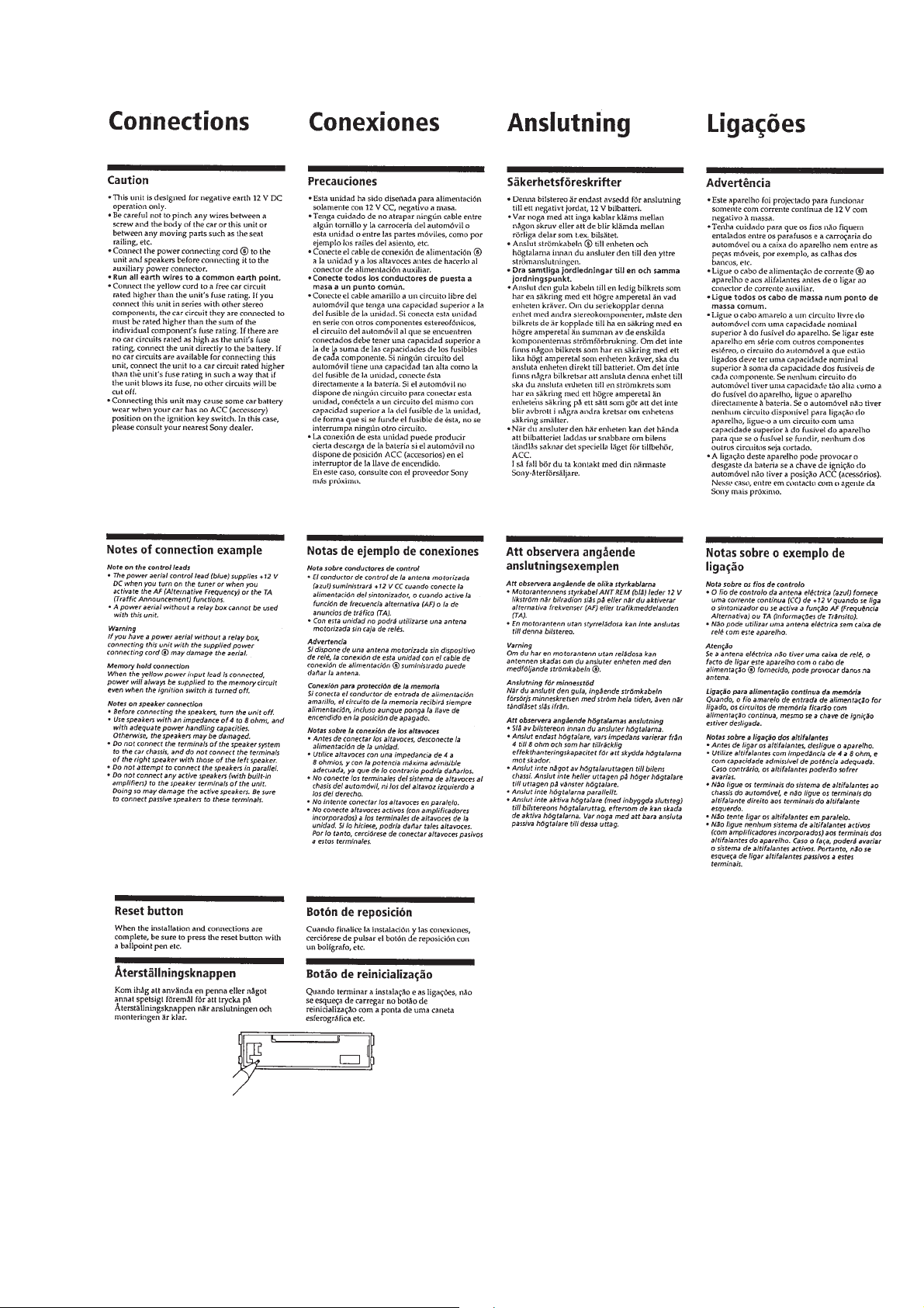
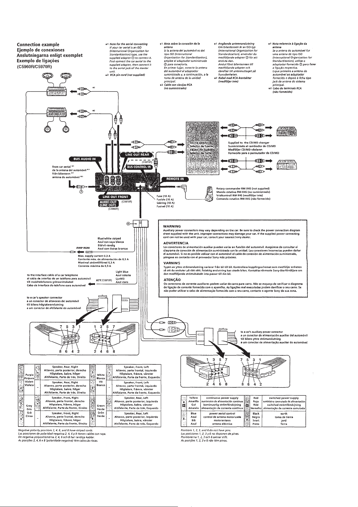
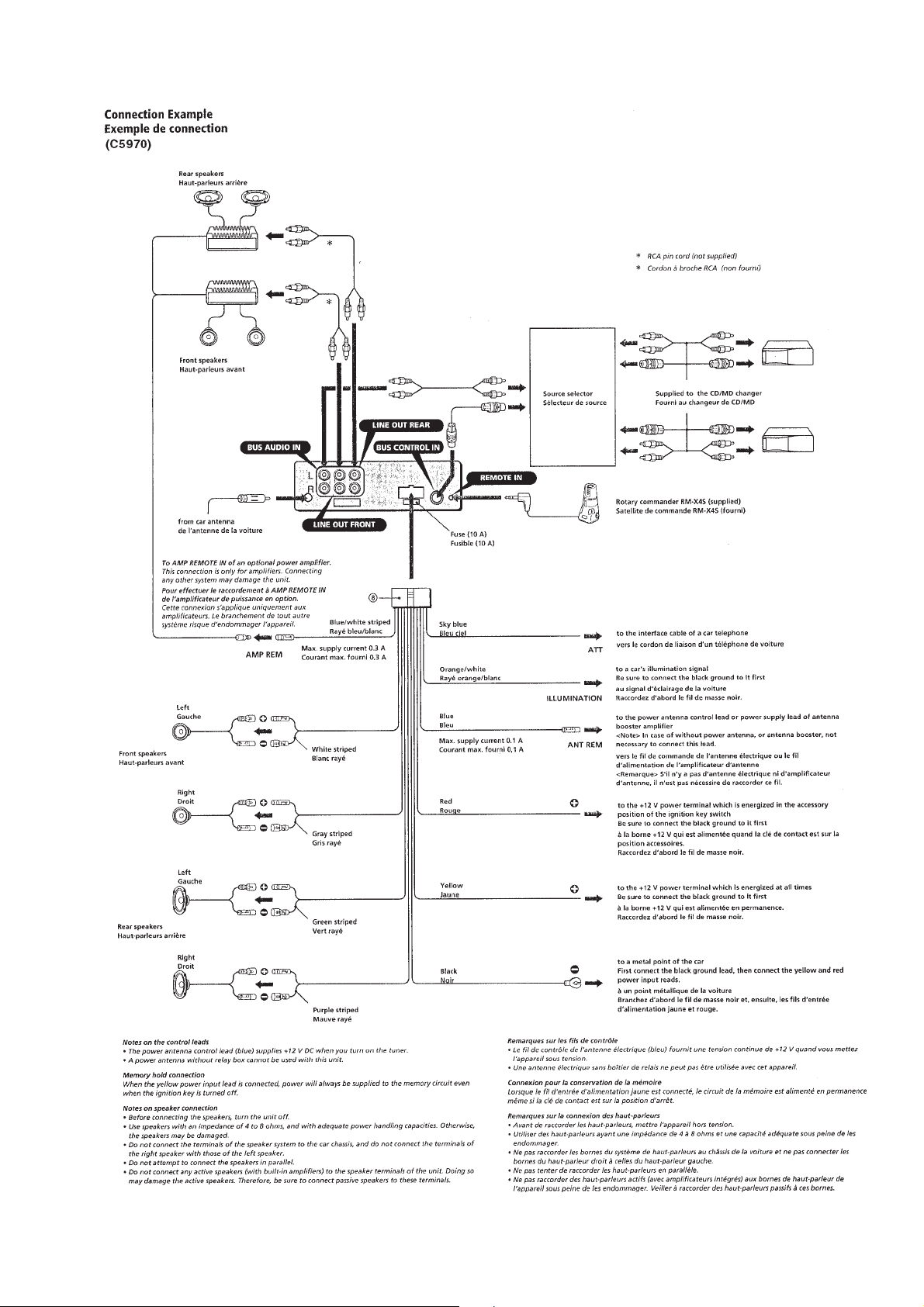
Page 1
MDX-C5960R/C5970/C5970R
SERVICE MANUAL
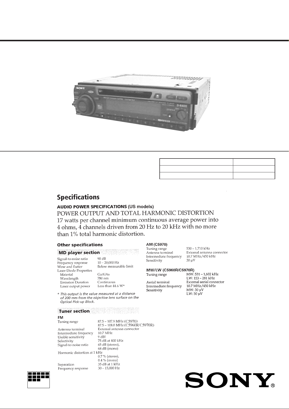
Photo: MDX-C5960R
SPECIFICATIONS
German Model
MDX-C5960R
US Model
Canadian Model
E Model
MDX-C5970
AEP Model
UK Model
MDX-C5970R
Model Name Using Similar Mechanism MDX-C7900/C7900R
Base Mechanism Type MG-164N-138
Optical Pick-Up Name KMS-241B/J1NP
MICROFILM
– Continued on next page –
FM/AM (MW/LW) MINIDISC PLAYER
Page 2
NOTES ON HANDLING THE OPTICAL PICK-UP
BLOCK OR BASE UNIT
The laser diode in the optical pick-up block may suffer electrostatic break-down because of the potential difference generated
by the charged electrostatic load, etc. on clothing and the human
body.
During repair, pay attention to electrostatic break-down and also
use the procedure in the printed matter which is included in the
repair parts.
The flexible board is easily damaged and should be handled with
care.
NOTES ON LASER DIODE EMISSION CHECK
Never look into the laser diode emission from right avove when
checking it for adustment. It is feared that you will lose your sight.
NOTES ON HANDLING THE OPTICAL PICK-UP BLOCK
(KMS-241B/J1NP).
The laser diode in the optical pick-up block may suffer electrostatic break-down easily. When handling it, perform soldering
bridge to the laser-tap on the flexible board. Also perform m easures
against electrostatic break-down suff iciently before the operation.
The flexible board is easily damaged and should be handled with
care.
SAFETY-RELATED COMPONENT WARNING!!
COMPONENTS IDENTIFIED BY MARK ! OR DOTTED
LINE WITH MARK ! ON THE SCHEMATIC DIA GRAMS
AND IN THE PARTS LIST ARE CRITICAL TO SAFE
OPERATION. REPLACE THESE COMPONENTS WITH
SONY PARTS WHOSE PART NUMBERS APPEAR AS
SHOWN IN THIS MANU AL OR IN SUPPLEMENTS PUBLISHED BY SONY.
ATTENTION AU COMPOSANT AYANT RAPPORT
À LA SÉCURITÉ!
LES COMPOSANTS IDENTIFIÉS P AR UNE MARQUE !
SUR LES DIAGRAMMES SCHÉMATIQUES ET LA LISTE
DES PIÈCES SONT CRITIQUES POUR LA SÉCURITÉ
DE FONCTIONNEMENT. NE REMPLACER CES COMPOSANTS QUE PAR DES PIÈCES SONY DONT LES
NUMÉROS SONT DONNÉS DANS CE MANUEL OU
DANS LES SUPPLÉMENTS PUBLIÉS PAR SONY.
laser-tap
OPTICAL PICK-UP FLEXIBLE BOARD
Notes on chip component replacement
• Never reuse a disconnected chip component.
• Notice that the minus side of a tantalum capacitor may be damaged by heat.
Flexible Circuit Board Repairing
• Keep the temperature of the soldering iron around 270 ˚C during repairing.
• Do not touch the soldering iron on the same conductor of the
circuit board (within 3 times).
• Be careful not to apply force on the conductor when soldering
or unsoldering.
CAUTION
Use of controls or adjustments or performance of procedures
other than those specified herein may result in hazardous radiation exposure.
– 2 –
Page 3

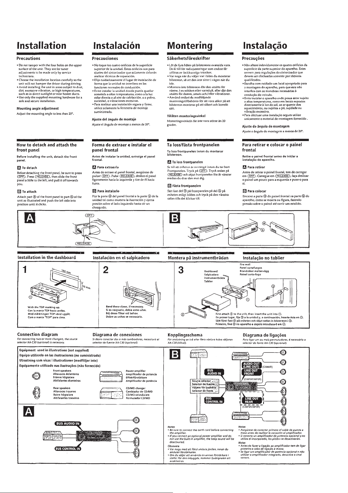
TABLE OF CONTENTS
1. GENERAL
Location of controls ........................................................ 4
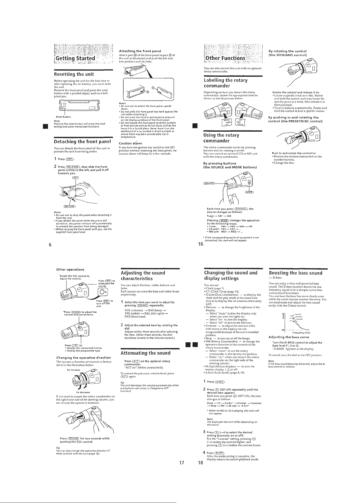
Resetting the unit ............................................................ 5
Detaching the front panel................................................ 5
Labelling the rotary commander..................................... 5
Using the rotary commander .......................................... 5
Adjusting the sound characterisitics............................... 5
Attenuating the sound ..................................................... 5
Changing the sound and display settings ....................... 5
Boosting the bass sound.................................................. 5
Installation....................................................................... 6
Connections..................................................................... 7
2. DISASSEMBLY ......................................................... 10
3. ELECTRICAL ADJUSTMENTS......................... 16
Test Mode........................................................................ 16
MD Section ..................................................................... 16
Tuner Section .................................................................. 16
4. DIAGRAMS
4-1. Block Diagram – SERVO Section – ............................... 19
4-2. Block Diagram – TUNER Section – .............................. 21
4-3. Block Diagram – MAIN Section – ................................. 23
4-4. Block Diagram
– DISPLAY/KEY CONTROL Section –........................ 25
4-5. Block Diagram – BUS CONTROL/
POWER SUPPLY Section – ........................................... 27
4-6. Notes for Printed Wiring Boards and
Schematic Diagrams ....................................................... 29
4-7. Printed Wiring Board – SERVO Board – ....................... 31
4-8. Schematic Diagram – SERVO Board (1/3) – ................. 33
4-9. Schematic Diagram – SERVO Board (2/3) – ................. 35
4-10. Schematic Diagram – SERVO Board (3/3) – ................. 37
4-11. Printed Wiring Board
– MAIN Board (Component Side) – .............................. 39
4-12. Printed Wiring Board
– MAIN Board (Conductor Side) – ................................ 41
4-13. Schematic Diagram – MAIN Board (1/4) – ................... 43
4-14. Schematic Diagram – MAIN Board (2/4) – ................... 45
4-15. Schematic Diagram – MAIN Board (3/4) – ................... 47
4-16. Schematic Diagram – MAIN Board (4/4) – ................... 49
4-17. Printed Wiring Board – KEY Board –............................ 51
4-18. Schematic Diagram – KEY Board – .............................. 53
4-19. IC Pin Function Description ........................................... 62
5. EXPLODED VIEWS................................................ 72
6. ELECTRICAL PARTS LIST ............................... 76
– 3 –
Page 4
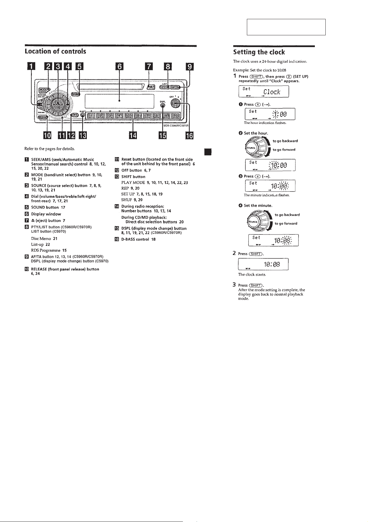
SECTION 1
GENERAL
This section is extracted from
instruction manual.
– 4 –
Page 5
– 5 –
Page 6
– 6 –
Page 7
– 7 –
Page 8
– 8 –
Page 9
– 9 –
Page 10
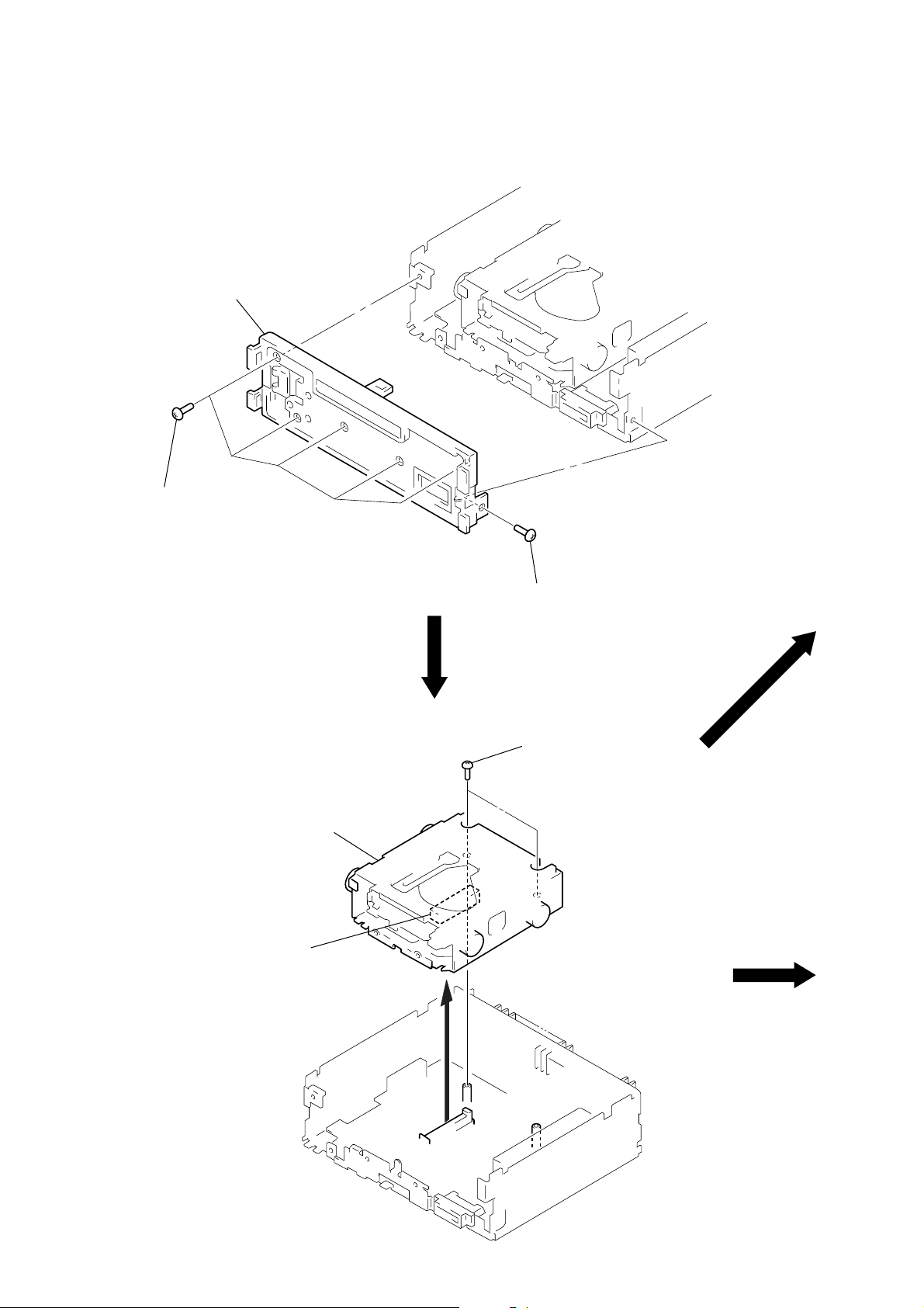
SECTION 2
DISASSEMBLY
Note: Follow the disassembly procedure in the numerical order given.
SUB PANEL
2
sub panel
1
five screws
(PTT2.6
×
6)
MECHANISM DECK (MG-164N-138)
3
mechanism deck
(MG-164N-138)
2
connector
(CN200)
1
screw
(PTT2.6
1
two screws
(PTT2.6
×
6)
×
4)
– 10 –
Page 11
MAIN BOARD, HEAT SINK
d
2
three screws
(PTT2.6
3
main board
4
insulating sheet
×
6) (ground point)
5
eight screws
(PTT2.6
6
×
10)
1
two screws
(PTT2.6
heat sink
×
10)
SERVO BOARD
1
2
two screws
(BVTT2
×
4)
sensor flexible board
(CN102)
2
two screws
(BVTT2
×
4)
3
servo board
1
flexible boar
(CN103)
– 11 –
Page 12
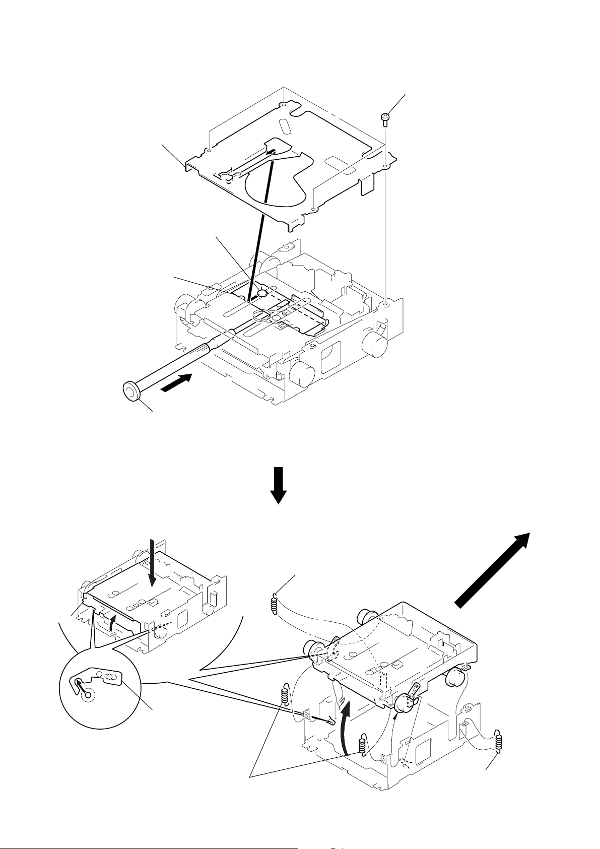
)
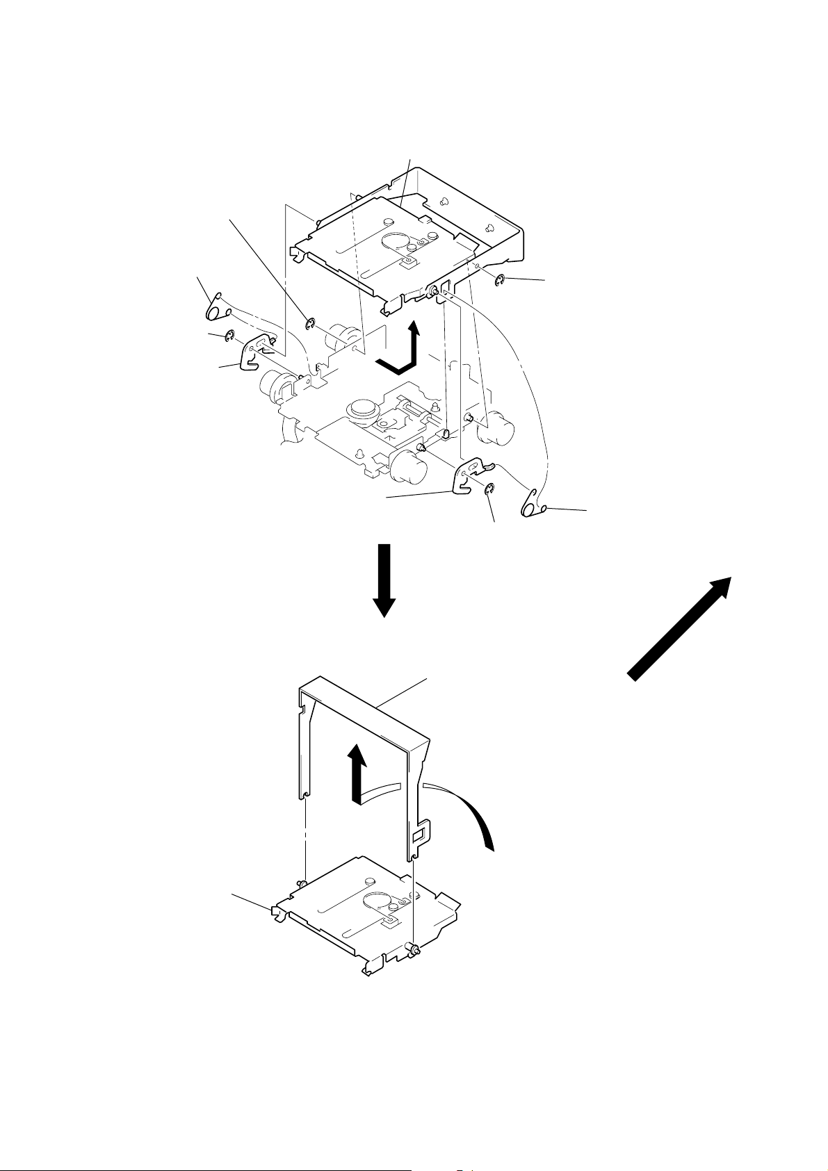
MD COVER ASS’Y
3
MD cover ass’y
shaft (MD cover guide)
cassette holder
1
four screws
(B2 × 3)
FLOAT BLOCK
float block
A
2
Pushing the Cassette Holder toward the direction A with a
screwdriver, etc., disengage the Shaft (MD Cover Guide) from
the slot in the MD Cover Assy.
Note:Take care not to scratch the optiocal Pick-up when pushing
the Cassette Holder with a screwdriver. etc.
3
Pushing an arrow A part, raise the float block
up ward at the front to release a lock.
1
A
tension spring (FL2)
lever (lock R)
lever (lock L)
2
two tension springs (FLOAT F)
– 12 –
1
tension spring (FL2
Page 13
LO MOTOR ASS’Y (LOADING) (M903)
4
Remove the bracket (LO)
in the direction of the arrow
A
.
1
Remove solders of motor (M903)
A
5
LO motor ass’y (loading)
(M903)
2
tension spring (rack)
3
claw
LEVER (LE) ASS’Y
2
stopper washer
1
3
roller (GLE)
2
lever (LE) ass’y
– 13 –
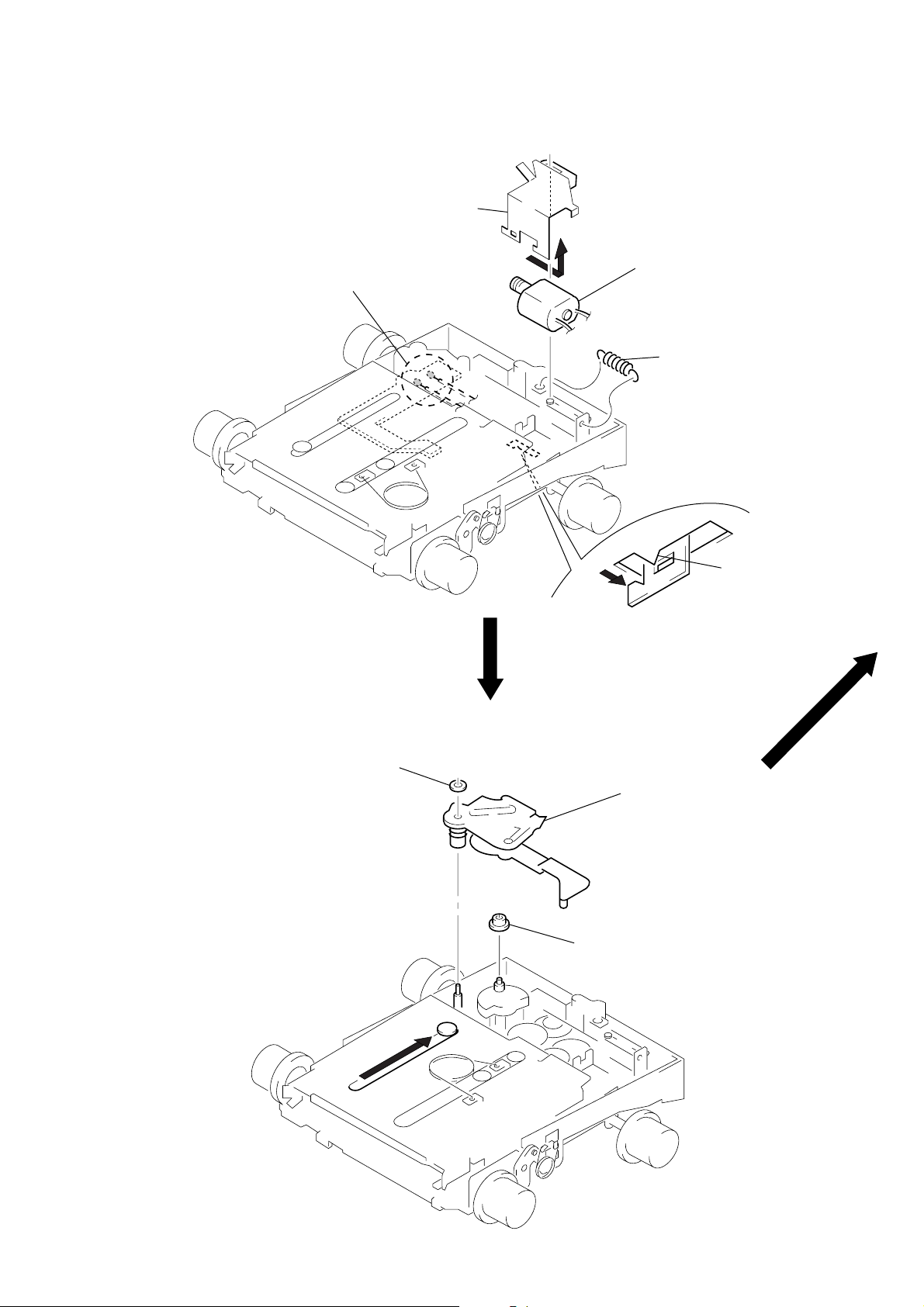
Page 14
HOLDER ASS’Y
2
type-E stopring 1.5
3
2
type-E stopring 1.5
1
spring (CHKG)
lever (lock R)
3
lever (lock L)
4
Remove the holder ass’y in the
direction of the arrow.
2
2
type-E stopring 1.5
1
type-E stopring 1.5
spring (CHKG)
CHUCKING ARM ASS’Y
holder ass’y
1
Remove the chucking arm ass’y
in the direction of the arrow.
– 14 –
Page 15
OPTICAL PICK-UP (KMS-241B/J1NP)
y
4
screw
(P1.7 × 1.8)
5
bracket (SL)
9
two screws
(P1.7 × 1.8)
!º
retainer (SP)
!¡
SP motor ass’y
(spindle) (M901)
7
screw
(B2 × 3)
2
two screws
(2 × 8)
3
sensor board
1
Remove solders of motors
(M901, M902)
8
base (SL)
6
SL motor ass’y
(sled) (M902)
7
optical pick-up
(KMS-241B/J1NP)
1
two screws
(K2 × 3)
2
shaft (SL2)
4
screw
(B2 × 3)
6
bearing (SL)
5
feed screw ass’
3
screw
(K2 × 3)
SL MOTOR ASS’Y (SLED) (M902), SP MOTOR ASS’Y (SPINDLE) (M901)
– 15 –
Page 16
SECTION 3
ELECTRICAL ADJUSTMENTS
TEST MODE
This set have the test mode function. In the test mode, FM Auto
Scan/Stop Level and AM (MW) Auto Scan/Stop Lev el adjustments
can be performed easier than it in ordinary procedure.
<Set the Test Mode>
1. Turn ON the regulated po wer supply. (The clock is displayed)
Note: Press the [OFF] button, if the clock is not displayed.
2. Push the preset [4] button.
3. Push the preset [5] button.
4. Press the preset [1] button for more than two seconds.
5. Then the display indicates all lights, the test mode is set.
<Release the Test mode>
1. Push the [OFF] button.
See the adjustment location from on page 18 for the adjustment.
MD SECTION
MD section adjustments are done automatically in this set.
TUNER SECTION
Cautions during repair
When the tuner unit is defective, replace it by a new one because its internal block is difficult to repair.
Note:
Adjust the tuner section in the sequence shown below.
1. FM Auto Scan/Stop Level Adjustment.
2. FM Stereo Separation Adjustmnet.
3. AM (MW) Auto Scan/Stop Level Adjustment.
4. RDS S-Meter Adjustment. (MDX-C5960R/5970R)
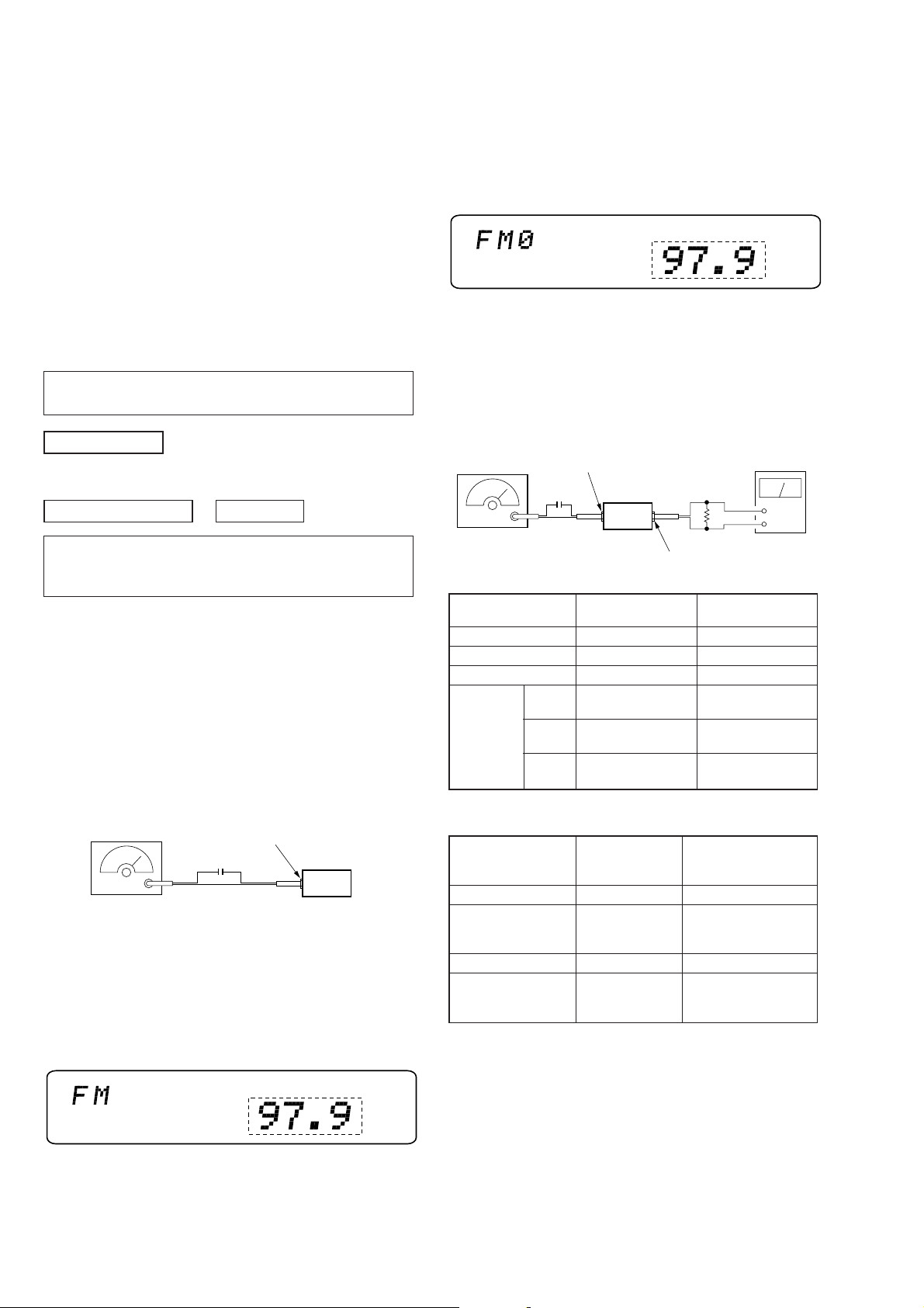
FM Auto Scan/Stop Level Adjustment
Setting:
[SOURCE] button: FM
FREQUENCY SELECT switch: FM 200 k (E model)
0 dB=1 µV
3. Adjust with the volume R V2 on TU1 so that the “FM” indication turns to “FM0” indication on the display window.
But, in case of already indicated “FM0”, turn the RV2 so that
put out light “0” indication and adjustment.
Display
SHUF
*1
*1: MDX-C5960R/C5970R indicate “98.00”.
Adjustment Location: See page 18.
FM Stereo Separation Adjustment
Setting:
[SOURCE] button: FM
FREQUENCY SELECT switch: FM 200 k (E model)
FM RF signal
generator
Carrier frequency 97.9 MHz 98.0 MHz
Output level 60 dB (1 mV) 70 dB (3.2 mV)
Mode stereo stereo
Modulation sub
antenna jack (J1)
0.01 µF
set
LINE OUT jack (CNP300)
MDX-C5970
main
19 kHz 7.5 kHz 7.5 kHz
pilot deviation (10%) deviation (10%)
1 kHz, 33.75 kHz 1 kHz, 16.25 kHz
deviation (45%) deviation (21.7%)
1 kHz, 33.75 kHz 1 kHz, 16.25 kHz
deviation (45%) deviation (21.7%)
10 k
level meter
Ω
+
–
MDX-C5960R/
C5970R
FM RF signal
generator
Carrier frequency: 97.9 MHz (MDX-C5970)
Output level : 22 dB (12.6
Mode : mono
Modulation : 1 kHz, 22.5 kHz deviation (30%)
98.0 MHz (MDX-C5960R/C5970R)
antenna jack (J1)
0.01 µF
µ
V)
Procedure:
1. Set to the test mode.
2. Push the [SOURCE] button and set to FM.
Display
SHUF
*1
set
Procedure:
FM Stereo
signal generator
output channel
L-CH L-CH A
R-CH L-CH Adjust RV4 on TU1
R-CH R-CH C
L-CH R-CH Adjust RV4 on TU1
Level meter Level meter
connection reading (dB)
for minimum reading.
for minimum reading.
L-CH Stereo separation: A-B
R-CH Stereo separation: C-D
The separations of both channels should be equal.
Specification: Separation more than 30 dB
Adjustment Location: See page 18.
B
D
– 16 –
Page 17
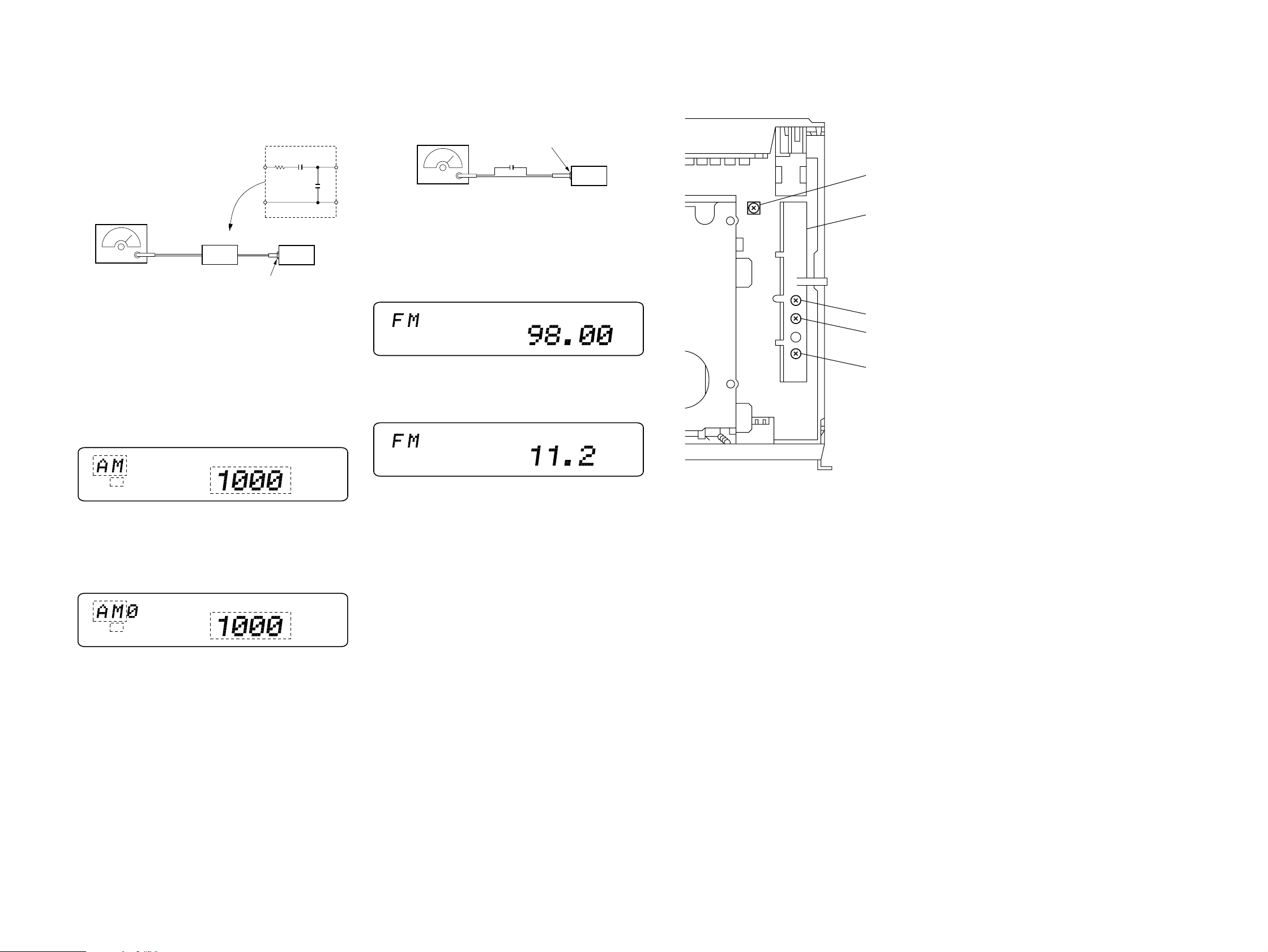
AM (MW) Auto Scan/Stop Level Adjustment
t
Setting:
[MODE] button (MDX-C5970): AM
[MODE] button (MDX-C5960R/C5970R): MW
FREQUENCY SELECT switch: AM 10 k (E model)
15 pF
30
Ω
65 pF
AM RF signal
generator
AM dummy antenna
(50 Ω)
antenna jack (J1)
Carrier frequency: 1000 kHz (MDX-C5970)
30% amplitude
modulation by
1 kHz signal
Output level : 33 dB (44.7
999 kHz (MDX-C5960R/5970R)
µ
V)
set
Procedure:
1. Set to the test mode. (See page 16)
2. Push the [SOURCE] button and set to FM.
3. Push the [MODE] button and set to AM (MDX-C5970) or MW
(MDX-C5960R/C5970R).
RDS S-Meter Adjustment (MDX-C5960R/C5970R)
Setting:
[SOURCE] button: FM
FM RF signal
generator
Carrier frequency: 98.0 MHz
Output level : 35 dB (56.2
Mode : mono
Modulation : no modulation
antenna jack (J1)
0.01 µF
µ
set
V)
Procedure:
1. Set to the test mode. (See page 16)
2. Push the [SOURCE] button and set to FM.
Display
SHUF
3. Push the preset [10] button.
4. Adjust RV1 on MAIN board so that the display indication is
“11.2”.
Display
Adjustment Location:
– SET UPPER VIEW –
RV1 RDS S-Meter Adjustment
(MDX-C5960R/C5970R)
TU1
RV1 AM (MW) Auto Scan/Stop Level Adjustmen
RV2 FM Auto Scan/Stop Level Adjustment
RV4 FM Sereo Separation Adjustment
Display
*2
*3
TP
*4
SHUF
4. Adjust with the volume RV1 on TU1 so that the “ AM” or “MW”
indication turns to “AM0” or “MW0” indication on the display window.
But, in case of already indicated “AM0” or “MW0”, turn the
RV1 so that put out light “0” indication and adjustment.
Display
*2
*3
TP
*4
SHUF
*2: MDX-C5960R/C5970R indicate “MW”.
*3: MDX-C5960R/C5970R indicate “999”.
*4: Only MDX-C5960R/C5970R indicate.
Adjustment Location: See page 18.
SHUF
Specification: Display indication : 10.8 to 11.6
Adjustment Location: See page 18.
– 17 – – 18 –
Page 18
MDX-C5960R/C5970/C5970R
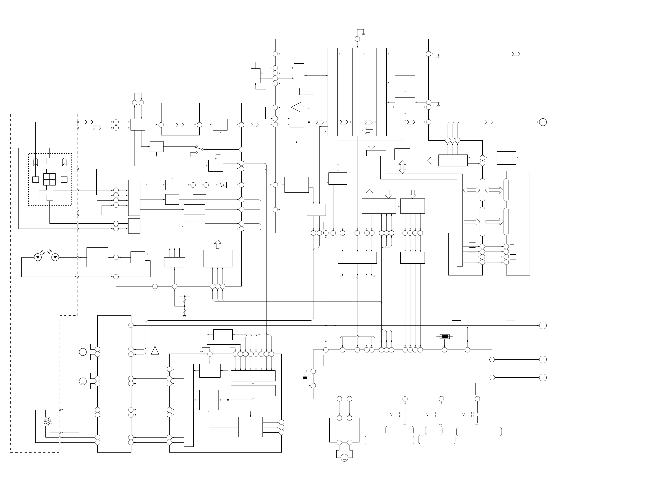
4-1. BLOCK DIAGRAM – SERVO Section –
SECTION 4
DIAGRAMS
100
EFMO
15
TX
IC301 (1/2)
ADDT
• SIGNAL PATH
23
: MD PLAY
FILI
59
PCO
58
61
FILTER
60
RF AMP,
FOCUS/TRACKING ERROR AMP
48 47
MORFI
MORFO
IC303
I
1
RF AMP
J
2
A
4
B
5
I-V
C
AMP
6
D
7
E
8
I-V
F
AMP
9
APC
PD
IN4R
IN4F
IN2F
IN2R
IN1F
IN1R
IN3F
IN3R
LD/PD
16PSB
3
4
29
30
19
18
14
15
11
10
AMP
SPFD
SPRD
RFO
B.P.F.
AT
AMP
12
46
3T
APCREF
IC306
WBL
B.P.F.
ABCD
AMP
WBL3TEQ
V-I
CONVERTER
F0CNT
20
APCREF
83
SFDR
92
SRDR
91
FFDR
88
FRDR
89
TFDR
86
TRDR
85
TEMP
ADFM
29 30
FOCUS
ERROR AMP
TRACKING
ERROR AMP
+3.3V
PWM GENERATOR
40
I
J
F
C B
I J
D A
E
DETECTOR
LASER DIODE
OPTICAL PICK-UP
(KMS-241B/J1NP)
2-AXIS
DEVICE
(FOCUS)
(TRACKING)
05
LDPD
ILCC
PD
M901
(SPINDLE)
M902
(SLED)
FCS+
FCS–
TRK+
TRK–
B
A
C
D
E
F
AUTOMATIC
POWER
CONTROL
Q302
FOCUS/TRACKING COIL DRIVE,
SPINDLE/SLED MOTOR DRIVE
OUT4F
6
M
8
OUT4R
OUT2F
27
M
25
OUT2R
OUT1F
21
23
OUT1R
OUT3F
12
10
OUT3R
IC302
AGCI
RF AGC
& EQ
EQ
PEAK &
BOTTOM
ADIN
COMMAND
SERIAL/
PARALLEL
CONVERTER,
DECODER
SCLK
SWDT
1716 18
PEAK HOLD
Q301
+3.3V
13
RECP
AUTOMATIC
POWER
CONTROL
DIGITAL
SERVO
SIGNAL
PROCESS
DIGITAL SERVO
SIGNAL PROCESSOR
IC301 (2/2)
WBL
XLAT
RF
AUX
PEAK
BOTM
ADFG
ABCD
FE
TE
SE
ABCD
AUX1
38
33
37
36
32
35
34
26
28
7465647566 63
FE
TE
AUX2
ABCD
ANALOG MUX
A/D CONVERTER
FROM CPU
INTERFACE
AUTO
SEQUENCER
73 62
SE
PEAK
XLRF
CKRF
DTRF
51
52
55
78
79
BOTM
CLTV
FILO
ASYO
ASYI
COMPA-
RFI
RATOR
ADFG
DEMODULATOR/
DECODER
F0CNT
10MHz
80
81
82
ADIP
X501
PLL
EFM/ACIRC
ENCODER/DECODER
SUBCODE
PROCESSOR
SPINDLE
SERVO
SPFD
SPRD
DQSY11SQSY14XINT
XRST
94 93
10
12
59 62 55 54 52 45 51 64 26 27 28 29
MD-RST
31
EXTAL
XTAL
32
7 6
LOADING
MOTOR DRIVE
IC305
M903
(LOADING)
5 4
RIN FIN
OUT1 OUT2
1 7
SHOCK PROOF
MEMORY CONTROLLER
51331
LEVEL SHIFT
IC502
61242
SQSY
CC-XINT
EJECT
LOAD
M
ATRAC
CPU
INTERFACE
SENS
SRDT
SWDT
9 8 5 6 7
SWDT
SENS
MD-SI
MD-SO
MD MECHANISM CONTROLLER
ON:When the disc loading start
and the disc eject completion.
SAMPLING
RATE
CONVERTER
DIGITAL
AUDIO
ENCODER/DECODER
INTERFACE
D-RAM
INTERNAL BUS
MONITOR
CONTROL
SCLK
XLAT
MNT0
1 2 3 4
13
LEVEL SHIFT
IC503
12
FOK
SCLK
XLAT
MNT0
MD-LAT
MD-CKO
IC501 (1/2)
C-SW
63
LOADING START/
EJECT END
DIN
DOUT
DADT
MNT1
MNT2
MNT3
135
246
SHOCK
XBUSY
SLOCK
MNT1
MNT2
MNT3
ON:When completion of
DIGITAL SIGNAL PROCESSOR,
EFM/ACIRC ENCODER/DECODER,
SHOCK PROOF MEMORY CONTROLLER,
ATRAC ENCODER/DECODER, 2M BIT D-RAM
21
22
24
LOADING
END
the disc loading.
IC301 (1/2)
BCK
LRCK
FS256
2526 27
XBCK
LRCK
FS256
CLOCK
GENERATOR
RESET
TH501
39
TEMP
E-SW
11 56
OSCI
OSCO
XOE
XWE
XRAS
XCAS
EMPHASIS
66
DEEMP
(LIMIT)
ON:When the optical pick-up is
inner position.
A-MUTE
16
17
D0 – D3A00 – A09
47, 46, 48, 49
32 – 29, 34 – 38, 43
41 22
45 3
44 4
42 23
LOCK
21
67
LIMIT-IN
DADT, BCK, LRCK, FS256
512FS OSC
IC304
D0 – D3
1, 2, 24, 25
A0 – A9
9 – 12, 14 – 18, 5
OE
WE
RAS
CAS
D-RAM
IC307
RESET, EMPHASIS
LOCK
MD-ATT
(Page 23)
A
X301
22.5792MHz
(Page 23)
B
C
(Page 23)
D
(Page 23)
– 19 – – 20 –
Page 19
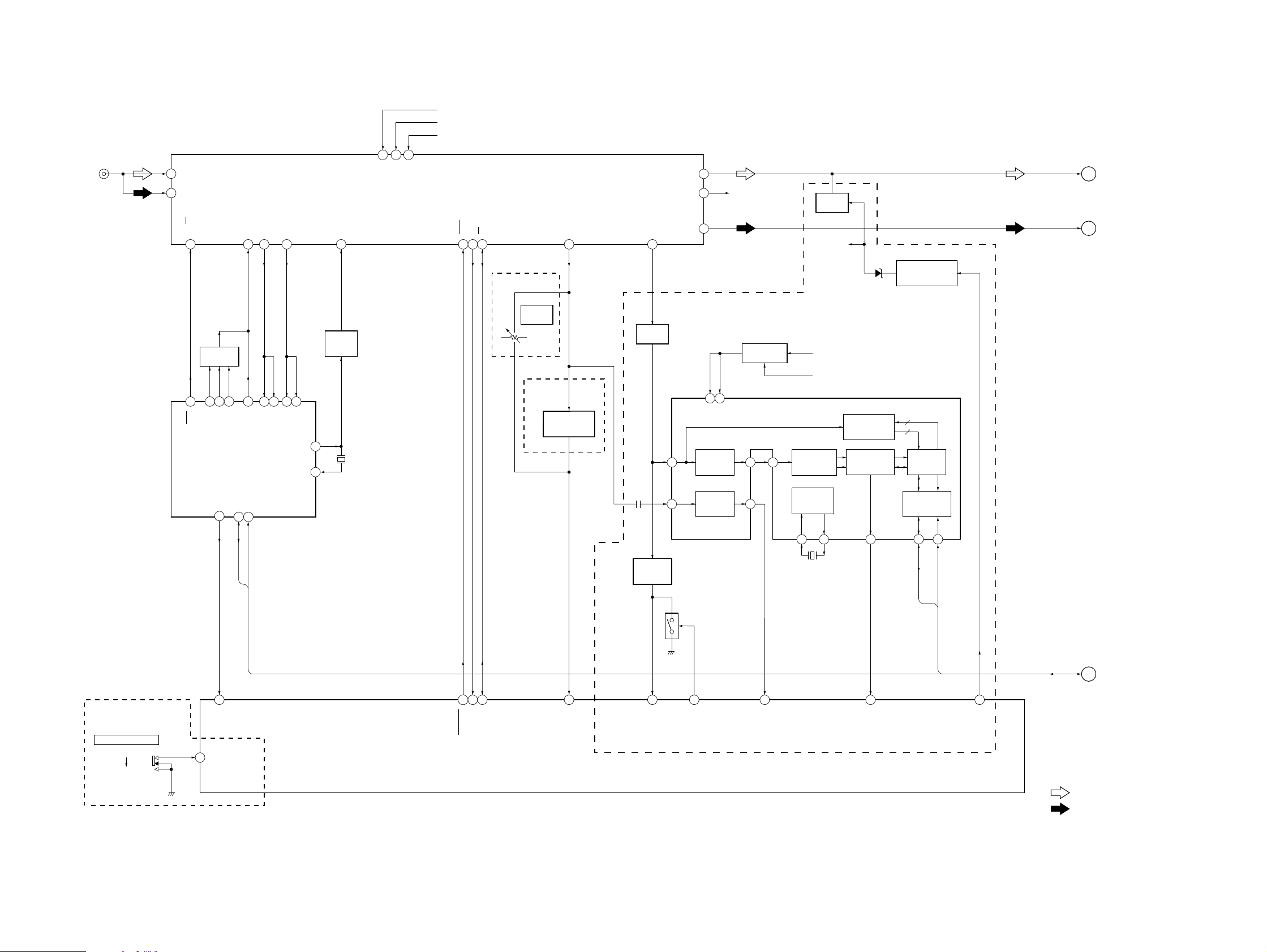
4-2. BLOCK DIAGRAM – TUNER Section –
FM/AM TUNER UNIT
2
1
FM-ANT
AM-ANT
TU1
LO/DX
4
FILTER
5 283
2
1
SEEK
LP HC
LP FM
SSTOP
16
LP AM
FM/AM PLL
IC100
SDA
13 12
VT
5
LP OUT
SCL
24
6
VCO
25
FM IN
21
15
AM IN
OSCOUT
FM/AM-IF
14
IF FM
IF AM
OSCIN
J1
(FM/AM ANTENNA)
10
9
AM OSC
13
AM OSC
BUFFER
Q4
X1
10.25MHz
8
FM +B
10
AM +B
MDX-C5960R/C5970/C5970R
FM B+
AM B+
TUNER B+
9
AM
FM
E
F
(Page 23)
(Page 23)
+B
ST/MONO
SD
SEEK
20
11
22
(C5960R/C5970R)
RV1
FM RDS
S-METER
(C5970)
S-METER
19
FM/AM SIGNAL
METER BUFFER
Q1
FM-DET
23
(C5960R/C5970R)
BUFFER
Q50
FM-LCH
FM-RCH
AM-DET
16
20
MPX
LVIN
18
16
12
14
7
VDDA
57 kHz
BAND-PASS
FILTER
MULTI
PATH
DETECTOR
VDDD
R-CH
OUT
B+ SWITCH
SC
18
MPTH
2
Q51
RDS DECODER
IC102
CIN
19
MUTING
Q101
BACKUP +5V
FM B+
CLOCKED
COMPARATOR
OSCILLATOR
& CLOCK
OSCI
OSCO
4
5
R-CH
DEMODULATOR
D5
SIGNAL
QUALITY
DECODER
RDS/RDBS
& DECODER
DAVN
8
MUTING
CONTROL SWITCH
Q103
5
4
INTERFACE
REGISTER
IIC BUS
SLAVE
TRANSCEIVER
SDA
SCL
9
10
(C5970: E model)
S701
FREQUENCY SELECT
MW 10K/FM 200K
MW 9K/FM 50K
05
100
BAND (9K-10K)
69
SSTOP
DATA
CLOCK
83
82
SEEKOUT
81
SD-IN
ST-MONO
MASTER CONTROLLER
IC700 (1/4)
53
S-METER (VSM)
BAND-PASS
FILTER
IC101
51
QUALITY
Q5
NOISE DET
DISCHARGE
SWITCH
35
NS-MASK
52
MPDH (MTP)
X2
4.332MHz
67
DAVN
DATA
CLOCK
62
TU-ATT
DATA, CLOCK
• SIGNAL PATH
(Page 23)
G
: FM
: AM (MW/LW)
– 21 –
– 22 –
Page 20
MDX-C5960R/C5970/C5970R
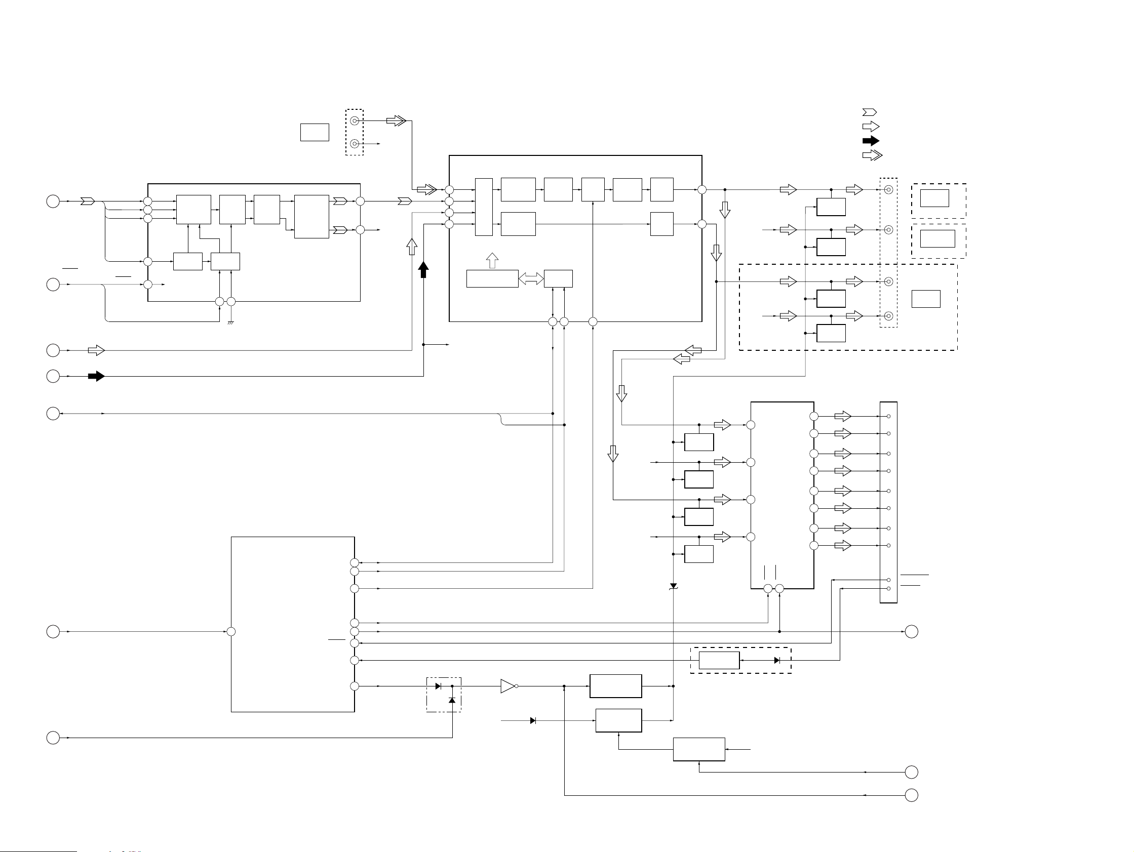
4-3. BLOCK DIAGRAM – MAIN Section –
CNP300 (1/2)
BUS
AUDIO IN
• SIGNAL PATH
: MD PLAY
(L)
INPUT SELECT,
(R)
R-CH
ELECTRICAL VOLUME
IC300
: FM
: AM (MW/LW)
: BUS AUDIO IN
(Page 20)
(Page 20)
(Page 22)
(Page 22)
(Page 22)
A
B
E
F
G
DADT,
BCK,
LRCK,
FS256
RESET,
EMPHASIS
FM
AM
DATA, CLOCK
DADT
BCK
LRCK
FS256
RESET
EMPHASIS
CNP300 (2/2)
(L)
(R)
(L)
(R)
CNP500 (1/2)
(POWER CONNECTOR)
1
FRONT L (+)
9
FRONT L (–)
4
FRONT R (+)
12
FRONT R (–)
2
REAR L (+)
10
REAR L (–)
3
REAR R (+)
11
REAR R (–)
15
TEST MODE
TEL-ATT
13
FRONT
LINE OUT
(C5970/C5970R)
AUDIO OUT
(LINE OUT)
(C5960R)
REAR
LINE OUT
DATA
CLOCK
VOLUME
CONTROL
CIRCUIT
IIC BUS
SCL
SDA
SOFT
MUTE
2625 24
INPUT
SELECTOR
CIRCUIT
LOUDNESS
CONTROL
CIRCUIT
LOUDNESS
CONTROL
CIRCUIT
PDL
11
12
28
1
SE2L
SE1L
SE3L
R-CH
DIGITAL CONTROL
D/A
IC101
VOUTL
VOUTR
SDA
SCL
AF ATT
12
9
R-CH
70
71
61
DATA
5
BCK
6
LRCK
4
XTI
1
RSTB
15
INPUT
INTERFACE
CLK
CONTROL
DIGITAL
FILTER
MODE
CONTROL
DM1
17 16
DM0
NOISE
SHAPER
MASTER CONTROLLER
CONVERTER
DIGITAL FILTER,
D/A CONVERTER
IC700 (2/4)
MUTE
TONE
CONTROL
CIRCUIT
R-CH
R-CH
FADER
FADER
OUT FL
OUT RL
D701
22
20
MUTING
Q302
MUTING
Q403
MUTING
Q303
MUTING
Q402
R-CH
(C5970/C5970R)
R-CH
POWER AMP
IC500
12
FL-IN
14
FR-IN
11
RL-IN
15
RR-IN
MUTE
22
4
ST-BY
FL+
FL–
FR+
FR–
RL+
RL–
RR+
RR–
5
3
21
23
9
7
17
19
MUTING
Q301
MUTING
Q401
MUTING
Q300
MUTING
Q400
(Page 20)
(Page 20)
LOCK
C
MD-ATT
D
05
LOCK IN
58
AMP ON
TESTIN
TEL-ATT
AU ATT
55AMP ATT
56
32
80
D700
60
COM +8V
Q702 (1/2)
D703
MUTING
CONTROL SWITCH
Q702 (2/2)
BATTERY OFF
MUTE DRIVER
Q704
LEVEL SHIFT
Q500
(C5970/C5970R)
MUTING
CONTROL SWITCH
Q703
D511
BATT B+
AMP ON
STB
MUTE
H
I
J
(Page 27)
(Page 28)
(Page 27)
– 23 – – 24 –
Page 21

4-4. BLOCK DIAGRAM – DISPLAY/KEY CONTROL Section –
EN801
VOLUME/BASS/TREBLE/
(LSW804: MDX-C5960R/C5970R only)
BALANCE/FADER CONTROL
MDX-C5960R/C5970/C5970R
J900
REMOTE IN
D900
49 72
RC-IN0
X1
93
X700
3.68MHz
RC-IN1
92
X0
LSW801 – 804,
LSW806 – 821
46
47
KEY-IN0
X1A
73
X701
32.768kHz
KEY-IN1
X0A
74
D912
ROTARY
ENCODER
EN801
VOL–
VOL+
106
107
RE-IN0
RE-IN1
LSW805
D-BASS
50
D-BASS IN
79
KEYACK
LCD SO13LCD CKO14LCD CE
104
KEY ACTIVE
SWITCH
Q905
37
AD-ON
BACKUP +5V
MASTER CONTROLLER
IC700 (3/4)
CNP801
FRONT PANEL SIDE
CN900
MAIN BODY SIDE
D813 – 817,
LSW802, 808, 811
1
1
12
NOSE-SW
BUZZER
DRIVE
Q701
15
BEEP
BZ1
(BUZZER)
LCDANG
40
LSW801, 804, 806,
LSW807, 809, 810,
(LSW804: MDX-C5960R/C5970R only)
R845
OSC
21
OSC OUT
05
20
OSC IN
SEG1 – SEG39, SEG48 – SEG73
32, 26 – 31, 33 – 38, 56 – 65,
75 – 90, 39 – 55, 66 – 74
LCD801
LIQUID CRYSTAL DISPLAY
18
17
19
CLK
STB
DATA
COM0 – COM7
100 – 93
KEY IN1 – KEY IN4
LIQUID CRYSTAL DISPLAY DRIVER
22 – 25
IC801
LSW812 – 821
PL801, 802
(LCD BACK LIGHT)
REGULATOR
Q806
REGULATOR
Q805, 807
3
DIMMER
4
POWER ON
LCD +10V
11 – 6
VLC0 – VLC5
CONTRAST
SWITCHING
Q901
LCD +10V
– 25 –
– 26 –
Page 22

MDX-C5960R/C5970/C5970R
4-5. BLOCK DIAGRAM – BUS CONTROL/POWER SUPPLY Section –
CNJ600
BUS CONTROL IN
(FOR SONY BUS)
RESET
DATA
CLK
BUS ON
BATT
2
5
4
6
7
BUS ON SWITCH
Q600
BACKUP +5V
RESET SIGNAL
GENERATOR
IC801
SONY BUS INTERFACE
IC600
RST
DATA
CLK
BUS ON
OUT
BATT
RESET
SWITCH
BUS ON
SWITCH
BATTERY
SWITCH
2
6
4
1
3
RST
DATA IN
DATA OUT
CLK IN
BUS
ON IN
BU IN
BACKUP +5V
RAM RESET
IC802
D916
S900
RESET
13
9
8
11
12
10
D702
MASTER CONTROLLER
IC700 (4/4)
102
RAMBU
RESET
90
86
HSTX
29
SYSRST
UNI SO
21
20
UNI SI
22
UNI CKIO
36
BUS-ON
BU-IN
76
PW-ON
FM-ON
TU-ON
STB
D804
+5V
(TUNER CIRCUIT B+)
TUNER B+
109
110
111
+5V
REGULATOR
Q6
D3
(AUDIO CIRCUIT B+)
FM B+
(FM CIRCUIT B+)
AM B+
(AM CIRCUIT B+)
COM +8V
BACKUP +5V
D802
11
10
6
8
9
5
AMP+B
ANT+B
FM8V
AM8V
COM8V
BU+B
REGULATOR
IC800
STB
4
VCC
MODE1
23
MODE2
D803
BATT B+
POWER AMP
(IC500) B+
7
(Page 24)
I
CNP500 (2/2)
(POWER CONNECTOR)
6
ANT REM
AMP REM
5
(Page 24)
(Page 24)
BATT B+
J
H
TH600
MUTE
AMP ON
D604
D603
BATTERY
DETECT
Q601
D606
D607
LEVEL SHIFT
Q603
LAMP ON (ILL ON)
ACC IN
ILL IN
MD MECHANISM CONTROLLER
IC501 (2/2)
60
BU-IN
BUS-ON
61
30
49
48
50
46
RESET
UNISI
UNICKIO
UNISO
LINKOFF
MDMON
LCD +10V
LCD DRIVER (IC801)/
ILLUMINATION LED B+
108
64
57
65MD-ON
10
REGULATOR
CONTROL SWITCH
Q906
REGULATOR
CONTROL SWITCH
Q255
LOAD +12V
LOADING MOTOR
DRIVER (IC305) B+
+3.3V
VCC
+3.3V
REGULATOR
IC401, Q401
ACCESSORY CHECK
Q900
B+ SWITCH
Q402, 403
DRIVER +5V
MOTOR/COIL DRIVER
(IC303) B+
CONVERTER
DC/DC
IC250
+10V
REGULATOR
Q903, 904
D913
D500
+12V
REGULATOR
Q254
B+ SWITCH
Q250, 251
F1
16
BATT
7
ACC
14
ILL IN
05
– 27 –
– 28 –
Page 23

4-6. NOTES FOR PRINTED WIRING BOARDS AND SCHEMATIC DIAGRAMS
MDX-C5960R/C5970/C5970R
Note on Printed Wiring Board:
• X : parts extracted from the component side.
• Y : parts extracted from the conductor side.
r
•
•
: Through hole.
¢
: internal component.
• b : Pattern from the side which enables seeing.
(The other layers' patterns are not indicated.)
Caution:
Pattern face side: Parts on the pattern f ace side seen from
(Conductor Side) the pattern face are indicated.
Parts face side: Parts on the parts face side seen from
(Component Side) the parts face are indicated.
Note on Schematic Diagram:
• All capacitors are in µF unless otherwise noted. pF: µµF
50 WV or less are not indicated except for electrolytics
and tantalums.
• All resistors are in Ω and 1/
specified.
¢
•
: internal component.
4
W or less unless otherwise
• C : panel designation.
Note:
The components identified by mark ! or dotted
line with mark ! are critical for safety.
Replace only with part
number specified.
Note:
Les composants identifiés par
une marque ! sont critiques
pour la sécurité.
Ne les remplacer que par une
piéce portant le numéro
spécifié.
• U : B+ Line.
• H : adjustment for repair.
• Power voltage is dc 14.4V and fed with regulated dc po w er supply
from ACC and BATT cords.
• Voltages are taken with a VOM (Input impedance 10 MΩ).
Voltage variations may be noted due to normal production tolerances.
• Waveforms are taken with a oscilloscope.
Voltage variations may be noted due to normal production tolerances.
• Circled numbers refer to waveforms.
• Signal path.
F : FM
f : AM (MW/LW)
L : BUS AUDIO IN
E : MD PLAY
• Abbreviation
CND : Canadian model.
G : German model.
– 29 –
Page 24

MDX-C5960R/C5970/C5970R
4-7. PRINTED WIRING BOARD – SERVO Board –
(Page 41)
• Semiconductor
Location
Ref. No. Location
D401 E-6
D501 E-4
IC301 B-5
IC302 C-2
IC303 B-3
IC304 C-5
IC305 F-6
IC306 B-4
IC307 B-8
IC401 E-6
IC501 F-3
IC502 D-5
IC503 D-4
Q301 A-4
Q302 C-1
Q401 D-6
Q402 E-7
Q403 E-7
– 31 – – 32 –
Page 25

4-8. SCHEMATIC DIAGRAM – SERVO Board (1/3) –
• See page 55 for Waveforms. • See page 58 for IC Block Diagrams.
The components identified by mark ! or dotted
line with mark ! are critical for safety.
Replace only with part number specified.
Les composants identifiés par une marque ! sont
critiques pour la sécurité. Ne les remplacer que
par une piéce portant le numéro spécifié.
• Voltages and waveforms are dc with respect
to ground under no-signal conditions.
no mark : MD PLAY
: Impossible to measure
∗
MDX-C5960R/C5970/C5970R
(Page 35)
– 33 – – 34 –
Page 26

MDX-C5960R/C5970/C5970R
4-9. SCHEMATIC DIAGRAM – SERVO Board (2/3) – • See page 55 for Waveforms. • See page 57 for IC Block Diagrams.
(Page 34)
(Page 37)
• Voltages and waveforms are dc with respect to ground
under no-signal conditions.
no mark : MD PLAY
: Impossible to measure
∗
– 35 – – 36 –
Page 27

4-10. SCHEMATIC DIAGRAM – SERVO Board (3/3) – • See page 55 for Waveforms.
• Voltages and waveforms are dc with respect to ground
under no-signal conditions.
no mark : MD PLAY
: Impossible to measure
∗
MDX-C5960R/C5970/C5970R
(Page 36)
(Page 43)
– 37 –
– 38 –
Page 28

MDX-C5960R/C5970/C5970R
4-11. PRINTED WIRING BOARD – MAIN Board (Component Side) –
• Semiconductor Location
(Component Side)
Ref. No. Location
D1 C-11
D3 F-11
D5 H-11
D6 F-9
D7 F-9
D8 G-13
D200 I-5
D202 F-4
D301 B-12
D500 B-5
D501 C-5
D503 C-6
D504 B-6
D505 B-6
D506 B-6
D507 B-8
D508 B-8
D509 B-9
D510 B-9
D511 B-5
D520 B-6
D521 A-9
D522 B-4
D600 B-2
D601 B-2
D602 B-3
D603 E-3
D604 C-3
D606 E-3
D607 B-13
D700 H-5
D701 H-4
D702 J-6
D703 F-4
D800 B-3
D801 B-3
D802 H-3
D803 D-3
D804 E-4
D900 C-1
D901 J-5
D902 K-12
D903 K-12
D904 K-12
D905 K-12
D907 K-12
D908 K-11
D909 K-11
D910 K-11
D911 K-11
Ref. No. Location
D912 J-10
D913 C-6
D914 K-11
D915 K-4
D916 K-4
IC100 E-11
IC101 E-9
IC102 I-12
IC250 I-5
IC300 F-8
IC600 B-4
IC700 I-8
IC801 J-2
IC802 J-2
Q1 C-11
Q4 D-11
Q5 F-9
Q6 C-10
Q50 H-13
Q51 I-14
Q101 H-11
Q102 G-11
Q103 H-11
Q250 I-5
Q251 H-6
Q254 E-5
Q255 F-4
Q300 B-10
Q301 B-11
Q302 C-7
Q303 C-6
Q400 B-10
Q401 B-11
Q402 C-8
Q403 C-8
Q500 B-5
Q600 D-3
Q601 D-4
Q603 B-4
Q701 F-3
Q702 G-5
Q703 G-5
Q704 G-4
Q900 D-6
Q901 J-6
Q905 J-9
Q906 J-5
– 39 – – 40 –
Page 29

4-12. PRINTED WIRING BOARD – MAIN Board (Conductor Side) –
MDX-C5960R/C5970/C5970R
• Semiconductor
Location
(Conductor Side)
Ref. No. Location
D502 C-3
IC500 A-7
IC800 E-1
Q903 H-2
Q904 H-3
(Page 52)
– 41 –
(Page 31)
– 42 –
Page 30

MDX-C5960R/C5970/C5970R
4-13. SCHEMATIC DIAGRAM – MAIN Board (1/4) – • See page 55 for Waveforms. • See page 60 for IC Block Diagrams.
(Page 38)
• Voltages and waveforms are dc with respect to ground
under no-signal (detuned) conditions.
no mark : FM
( ) : AM (MW)
[]: LW
〈〈 〉〉 : MD PLAY
(Page 45)
(Page 48)
– 43 – – 44 –
(Page 49)
Page 31

4-14. SCHEMATIC DIAGRAM – MAIN Board (2/4) –
MDX-C5960R/C5970/C5970R
(Page
44)
(Page 49)
• Voltages are dc with respect to ground under no-signal
(detuned) conditions.
no mark : FM
– 45 – – 46 –
Page 32

MDX-C5960R/C5970/C5970R
4-15. SCHEMATIC DIAGRAM – MAIN Board (3/4) – • See page 55 for Waveforms. • See page 60 for IC Block Diagrams.
(Page 44)
• Voltages and waveforms are dc with respect to ground
under no-signal (detuned) conditions.
no mark : FM
( ) : AM (MW)
[]: LW
– 47 – – 48 –
(Page 49)
Page 33

4-16. SCHEMATIC DIAGRAM – MAIN Board (4/4) – • See page 61 for IC Block Diagrams.
(Page
44)
MDX-C5960R/C5970/C5970R
(Page 45)
(Page 48)
(Page 53)
• Voltages are dc with respect to ground under no-signal
(detuned) conditions.
no mark : FM
( ) : AM (MW)
[]: LW
〈〈 〉〉 : MD PLAY
– 49 – – 50 –
Page 34

MDX-C5960R/C5970/C5970R
4-17. PRINTED WIRING BOARD – KEY Board –
• Semiconductor
Location
(Component Side)
Ref. No. Location
D811 C-3
D812 B-3
D813 A-4
D814 A-2
D815 B-1
D816 C-2
D817 A-11
IC801 B-8
Q806 C-4
Q807 B-1
• Semiconductor
Location
(Conductor Side)
Ref. No. Location
D802 B-12
D803 B-12
D804 B-12
D806 B-5
D807 B-6
D808 A-12
D819 B-2
Q805 B-2
(Page 41)
– 51 – – 52 –
Page 35

4-18. SCHEMATIC DIAGRAM – KEY Board – • See page 56 for Waveforms.
(Page 50)
MDX-C5960R/C5970/C5970R
– 53 – – 54 –
• Voltages and waveforms are dc with respect to ground
under no-signal (detuned) conditions.
no mark : FM
Page 36

• Wavef orms
– SERVO Board –
– MAIN Board –
– KEY Board –
1 IC302 @§ (TE) (MD PLAY Mode)
2 IC302 #¢ (FE) (MD PLAY Mode)
3 IC302 #• (RF) (MD PLAY Mode)
Approx.
0.5 Vp-p
Approx.
0.3 Vp-p
6 IC501 #¡ (EXTAL) (MD PLAY Mode)
2.7 Vp-p
0.1 µs
7 IC304 3 (IN) (MD PLAY Mode)
3.5 Vp-p
44 ns
1 IC100 9 (OSC IN) (FM/AM (MW) Mode)
2.7 Vp-p
94 ns
2 IC102 5 (OSC1) (FM Mode)
2.8 Vp-p
224 ns
3 IC250 2 SWE (MD PLAY Mode)
6 IC700 (£ (X1)
271 ns
5.8 Vp-p
1 IC801 @º (OSC IN)
2.8 Vp-p
3.5 µs
1.2 Vp-p
4 IC301 @∞ (LRCK) (MD PLAY Mode)
3.5 Vp-p
23 µs
5 IC301 @§ (XBCK) (MD PLAY Mode)
4.5 Vp-p
14.2 Vp-p
24 µs
4 IC250 3 TC (MD PLAY Mode)
1.1 Vp-p
12 µs
5 IC700 &¢ (XOA)
2.1 Vp-p
356 µs
30 µs
– 55 – – 56 –
Page 37

• IC Block Diagrams
– SERVO Board –
IC101 PCM1718E/2K
XTI
DGND
VDD
LRCIN
DIN
BCKIN
ZERO
D/C_R
VOUTR
AGND
1
2
3
4
5
6
7
8
9
10
INPUT
INTERFACE
DIGITAL
FILTER
NOISE SHAPER
5 LEVEL
DAC
LOWPASS
FILTER
CMOS
AMP
CONTROL
IC301 CXD2652AR
EFMO
DVSS
TEST3
TEST2
99 98 97 96 95 94 93
SUBCODE
CLOCK
MNT0
MNT1
MNT2
MNT3
SWDT
SCLK
XLAT
SRDT
SENS
XRST
SQSY
DQSY
RECP
XINT
OSCI
OSCO
XTSL
DVSS
DIN
DOUT
100
1
2
MONITOR
CONTROL
3
4
5
6
CPU I/F
7
8
9
10
11
PROCESSOR
12
13
14
15
TX
16
17
GENERATOR
18
19
NC
20
21
22
CLK
TEST1
EACH
BLOCK
EACH
BLOCK
MODE
CONTROL
5 LEVEL
DAC
LOWPASS
FILTER
CMOS
AMP
FGIN
SPINDLE
SERVO
ADIP
DECODER
EACH
BLOCK
SPFD
SPRD
DIGITAL
AUDIO
XTO
20
CLKO
19
MUTE
18
DM1
17
DM0
16
RSTB
15
FORMAT
14
D/C_L
13
VOUTL
12
VCC
11
SFDR91SRDR90FS489FRDR88FFDR87DVDD86TFDR85TRDR84LDDR83APCREF82DTRF81CKRF80XLRF79F0CNT78ADFG77APC76DCHG
92
PWM
SHOCK RESISTANT
MEMORY CONTROLLER
SAMPLING
I/F
RATE
CONVERTER
GENERATOR
SERVO
DSP
CONVERTER
AUTO
A/D
SEQUENCER
ANALOG
DECODER
ENCODER/
EFM/ACIRC
COMP
MUX
PLL
75
AUX2
74
TE
73
SE
72
AVSS
71
ADRB
70
ADRT
69
AVDD
68
ADIO
67
VC
66
AUX1
65
FE
64
ABCD
63
BOTM
62
PEAK
61
CLTV
60
FILO
59
FILI
58
PCO
57
PDO
56
AVSS
55
RFI
54
BIAS
53
AVDD
52
ASYI
51
ASYO
ADDT
DADT
LRCK
23
24
25
28
26
27
XBCK
DVDD
FS256
ATRAC
ENCODER/DECODER
ADDRESS/DATA BUS A00 - A11, D0 - D3
40
39
A1138A0837A0736A0635A0534A0433A1032A0031A0130A0229A03
41
DVSS
XOE
42
43
XCAS
A09
44
XRAS
XWE
50
49D348D247D046D145
MVCI
– 57 –
Page 38

IC302 CXA2523R
MORFO47MORFI46RFO45OPN
48
–
+
RFA1
+
–
AA
BB
CC
DD
EE
FF
–
–
–
–
–
–
–
GRVA
1
2
1
2
RFA2
CFST
+
–
+
–
FBAL
HLPT
GRV
1I
2J
CVB
3VC
4A
IVR
5B
IVR
6C
IVR
7D
IVR
8E
IVR
9F
IVR
GSW IV
+
–
+
–
+
–
+
–
+
–
+
–
+
–
OPO43ADDC42COMPP41COMPO40AGCI39RF AGC38RF37PEAK
44
EE'
USROP
+
+
+
+
+
+
–
–
–
–
+
+
–1
–2
–2
–1
FF'
+
–
BPF3T
PTGR
ABCDA
FEA
BPF22
WBL
ATA
WBL
–
+
–
+
EFB TESW
RF AGC EQ
USRC
PEAK
BOTTOM
WBL
ADIP
PTGR
PEAK3T
P-P
AGC
WBL
3T
EQ
3T
3T WBL
PBH
DET
–1
–2
–1
–2
TEMP
DET
EQ
BPFC
SEA
TEA
VI CONV
TG
TG
36
BOTM
35
ABCD
34
FE
33
AUX
32 ADFG
31 ADAGC
30 ADIN
29 ADFM
28 SE
27 CSLED
26 TE
25 WBLADJ
15
AUXSW
TEMPR
COMMAND
SCRI - PARA
DECODE
17
16
SCLK
SWDT
BGR
VREF
24
23
22
21
20
19
18
XLAT
XSTBY
F0CNT
VREF
EQADJ
3TADJ
VCC
10PD
11APC
12APCREF
+
–
+
–
14
13
GND
TEMPI
– 58 –
Page 39

IC303 BH6511FS-E2
CAPA–
CAPA+
IN2R
IN2F
VM2
OUT2F
PGND2
OUT2R
VM12
OUT1R
PGND1
OUT1F
VM1
32 31 30 29 28 27 26 25 24 23 22 21 20 19 18 17
IN4F
AMP
AMP
VM4
INTERFACE
CHARGE
PUMP.
OSC
INTERFACE
1 2 3 4 5 6 7 8 9 10 11 12 13 14 15 16
VG
GND
IN4R
OUT4F
PGND4
AMP
OUT4R
VM34
AMP
OUT3R
PGND3
AMP
AMPAMPAMP
OUT3F
INTERFACE
PREDRIVEPREDRIVE
PREDRIVEPREDRIVE
INTERFACE
VM3
IC305 BA6287F
1
OUT1
VM
2
8
GND
7
OUT2
IN1F
IN3F
IN1R
IN3R
V
PSB
DD
V
DD
PSB
DRIVER DRIVER
TSD
3
VCC
FIN
POWER
SAVE
4
CONTROL LOGIC
IC307 MN41V4400TT-08S
1
D1
2
D2
XWE
3
4
XRAS
NC
5
NC
6
7
NC
A9
8
A0
9
10
A1
A2
11
12
A3
A0–A9
A0–A9
ADDRESS BUFFER
CLOCK OSC
COLUMN DECODER
SENSE REFRESH AMP
INPUT/OUTPUT CONTROL SWITCH
MEMORY CELL
(4194204 BIT)
ROW DECODER
6
VREF
5
RIN
GND
26
D4
25
24
D3
XCAS
23
XOE
22
BUFFER
(4) INPUT
BUFFER
(4) OUTPUT
21
NC
20
NC
NC
19
A8
18
A7
17
16
A6
15
A5
1413
A4VDD
– 59 –
Page 40

– MAIN Board –
IC100 TDA7427AD
LP OUT
11 BIT
PROGRAMMABLE
COUNTER
SWITCH
OUT
INLOCK
CHARGE
PUMP
DETECTOR
PARATOR
+
–
SWITCH
LP1/LP2
3 41 2 7
VREF
LP HC
LP FM
LP AM
PROGRAMMABLE
PHASE
COM-
SWITCH
SWM/DIR
5 BIT
COUNTER
PRE
COUNTER
SWITCH
SWM/DIR
16 BIT
PROGRAMMABLE
COUNTER
LOGIC
PORT
EXTENSION
5 6 11 129
DOUT3
DOUT4
TEST
8
DOUT5
DOUT6
FM/AM
SWITCH
TIMER
14 BIT
PROGRAMMABLE
COUNTER
REFERENCE
OSCILLATOR
10
OSCIN
OSCOUT
VDD2
AM IN
GND-AM
NC
NC
FM IN
POWER ON RESET
11 – 21 BIT
PROGRAMMABLE
GND-SIG
SUPPLY &
CONTROL
COUNTER
VDD1
ADDR
IIC BUS
INTERFACE
SCL
DOUT1/INLOCK
HFREF
SSTOP
DOUT2
FM/AM
SWITCH
13 14
SDA
IF FM
1516171819202122232425262728
IF AM
IC102 SAA6588T-118 (MDX-C5960R/C5970R)
6
VSSD
VREF
17
SIGNAL QUALITY
CLOCK
DATA
87
DAVN
VDDD
MPX
DECODER
445
INTERFACE
REGISTER
VSSA
15
POWER SUPPLY
& RESET
LVIN
20
MULTI
PATH
DETECTOR
2
1
MRO
MPTH
CIN
19
CLOCKED
COMPARATOR
RDS/RDBS
DEMODULATOR
TEST
CONTROL
3
TCON
SCOUT
18
BAND-PASS FILTER
OSCILLATOR
& CLOCK
4 5
OSCO
57kHz
8th ORDER
RDS/RDBS
DECODER
OSCI
VDDA
14
CLOCK
DATA
IIC BUS SLAVE
TRANSCEIVER
9 10
1316
SDA
AFIN
SCL
PAUSE
DETECTOR
IC250 NJM2360AM (TE2)
MAD
PSWN
11
12
Q2
1CS
Q1
2ES
3CT
4GND
VREF
1.25V
QS
R
+
–
CT OSC
COMP
Ipk
8CD
7SI
6V+
5 INVIN
– 60 –
Page 41

IC300 TDA7462D013TR
SE3L
SE3R
MUTE
SDA
SCL
PAUSE
OUT FL
OUT FR
OUT RL
OUT RR
SUBOUT+
SUBOUT–
VDD
GND
CREF
SE1L
SE1R
MD+
MD–
CDL+
CDL–
CDR–
CDR+
PDR
PDGND
PDL
SE2L
SE2R
INPUT
GAIN &
AUTO
ZERO
PAUSE
DETECT
INPUT MULTIPLEXER &
MIXING STAGE
REAR SIDE
SELECTOR
FRONT SIDE
SELECTOR
LOUDNESS
CONTROL
CIRCUIT
INPUT
GAIN
BEEP
LOUDNESS
CONTROL
CIRCUIT
SOFT
MUTE
VOLUME
CONTROL
CIRCUIT
COMPANDER
TREBLE/
BASS
CONTROL
CIRCUIT
SUBWOOFER
OUT
FADER
SUBWOOFER
LP
IIC
BUS
DIGITAL CONTROL CIRCUIT
POWER
SUPPLY
FRONT
FADER
FRONT
FADER
REAR
FADER
REAR
FADER
VOICE BANDPASS
HP LP
SDA
SCL
1
2
3
4
5
6
7
8
9
10
11
12
13
14
15
16
17
18
19
20
21
22
23
24
25
26
27
28
IC600 BA8270F-E2
BUS ON
SWITCH
RESET
SWITCH
BATTERY
SWITCH
BUS ON
1
2
RST
BATT
3
4
CLK
5
VREF
6
DATA
GND
7 8
14
13
12
11
10
9
VCC
RST
BUS ON
CLK IN
BU IN
DATA IN
DATA OUT
IC800 BA3918-V3
1
NC
2 3
MODE2
4
STB
MODE1
–
+
– 61 –
REGULATOR
OVER VOLTAGE
PROTECT
5 6 7 8 9 10 1211
VDD
AMP
VCC
ANT
COM
–
+
AM
–
+
–
+
FM
GND
Page 42

4-19. IC PIN FUNCTION DESCRIPTION
• SERVO BOARD IC301 CXD2652AR
(DIGITAL SIGNAL PROCESSOR, DIGITAL SERVO PROCESSOR, EFM/ACIRC ENCODER/DECODER,
SHOCK PROOF MEMORY CONTROLLER, ATRAC ENCODER/DECODER, 2M BIT D-RAM)
Pin No. Pin Name I/O Function
1 MNT0 O
2 MNT1 O
3 MNT2 O
4 MNT3 O
5 SWDT I
6 SCLK I
7 XLAT I
8 SRDT O (3)
9 SENS O (3)
10 XRST I Reset signal input from the MD mechanism controller (IC501) “L”: reset
11
SQSY O
Focus OK signal output to the MD mechanism controller (IC501)
“H” is output when focus is on (“L”: NG)
Track jump detection signal output to the MD mechanism controller (IC501)
Busy monitor signal output to the MD mechanism controller (IC501)
Spindle servo lock status monitor signal output to the MD mechanism controller (IC501)
Writing serial data signal input from the MD mechanism controller (IC501)
Serial data transfer clock signal input from the MD mechanism controller (IC501)
Serial data latch pulse signal input from the MD mechanism controller (IC501)
Reading serial data signal output to the MD mechanism controller (IC501)
Internal status (SENSE) output to the MD mechanism controller (IC501)
Subcode Q sync (SCOR) output to the MD mechanism controller (IC501)
“L” is output every 13.3 msec Almost all, “H” is output
12
13 RECP I
14 XINT O Interrupt status output to the MD mechanism controller (IC501)
15 TX I
16 OSCI I System clock signal (512Fs=22.5792 MHz) input from the oscillator circuit
17 OSCO O System clock signal (512Fs=22.5792 MHz) output terminal Not used (open)
18 XTSL I
19 RVDD — Power supply terminal (+3.3V) (digital system)
20 RVSS — Ground terminal (digital system)
21
22
23
24
25
26
27 FS256 O
28 DVDD — Power supply terminal (+3.3V) (digital system)
29 to 32
33
34 to 38
39
40 DVSS — Ground terminal (digital system)
41 XOE O Output enable signal output to the D-RAM (IC307) “L” active
42 XCAS O Column address strobe signal output to the D-RAM (IC307) “L” active
43 A09 O Address signal output to the D-RAM (IC307)
44 XRAS O Row address strobe signal output to the D-RAM (IC307) “L” active
45 XWE O Write enable signal output to the D-RAM (IC307) “L” active
DQSY O
DIN I Digital audio signal input terminal when recording mode Not used (fixed at “L”)
DOUT O Digital audio signal output terminal when playback mode Not used (open)
ADDT I Recording data input terminal Not used (fixed at “L”)
DADT O Playback data output to the PCM1718E (IC101)
LRCK O L/R sampling clock signal (44.1 kHz) output to the PCM1718E (IC101)
XBCK O Bit clock signal (2.8224 MHz) output to the PCM1718E (IC101)
A03 to A00 O Address signal output to the D-RAM (IC307)
A10 O
A04 to A08 O Address signal output to the D-RAM (IC307)
A11 O
Digital In U-bit CD format subcode Q sync (SCOR) output terminal
“L” is output every 13.3 msec Almost all, “H” is output Not used (open)
Laser power selection signal input terminal
“L”: playback mode, “H”: recording mode (fixed at “L” in this set)
Recording data output enable signal input terminal
Writing data transmission timing input (Also serves as the magnetic head on/off output)
Not used (fixed at “L”)
Input terminal for the system clock frequency setting
“L”: 45.1584 MHz, “H”: 22.5792 MHz (fixed at “H” in this set)
Clock signal (11.2896 MHz) output to the PCM1718E (IC101)
Address signal output to the external D-RAM Not used (open)
Address signal output to the external D-RAM Not used (open)
– 62 –
Page 43

Pin No. Pin Name I/O Function
46 D1 I/O
47 D0 I/O
48 D2 I/O
Two-way data bus with the D-RAM (IC307)
49 D3 I/O
50 MVCI I Digital in PLL oscillation input from the external VCO Not used (fixed at “L”)
51 ASYO O Playback EFM full-swing output terminal
52 ASYI I (A) Playback EFM asymmetry comparator voltage input terminal
53 AVDD — Power supply terminal (+3.3V) (analog system)
54 BIAS I (A) Playback EFM asymmetry circuit constant current input terminal
55 RFI I (A) Playback EFM RF signal input from the CXA2523R (IC302)
56 AVSS — Ground terminal (analog system)
57 PDO O (3) Phase comparison output for clock playback analog PLL of the playback EFM Not used (open)
58 PCO O (3) Phase comparison output for master clock of the recording/playback EFM master PLL
59 FILI I (A) Filter input for master clock of the recording/playback master PLL
60 FILO O (A) Filter output for master clock of the recording/playback master PLL
61 CLTV I (A) Internal VCO control voltage input of the recording/playback master PLL
62 PEAK I (A) Light amount signal (RF/ABCD) peak hold input from the CXA2523R (IC302)
63 BOTM I (A) Light amount signal (RF/ABCD) bottom hold input from the CXA2523R (IC302)
64 ABCD I (A) Light amount signal (ABCD) input from the CXA2523R (IC302)
65 FE I (A) Focus error signal input from the CXA2523R (IC302)
66 AUX1 I (A) Auxiliary signal (I
3 signal/temperature signal) input terminal Not used (fixed at “H”)
67 VC I (A) Middle point voltage (+1.65V) input from the CXA2523R (IC302)
68 ADIO O (A) Monitor output of the A/D converter input signal Not used (open)
69 AVDD — Power supply terminal (+3.3V) (analog system)
70 ADRT I (A) A/D converter operational range upper limit voltage input terminal (fixed at “H” in this set)
71 ADRB I (A) A/D converter operational range lower limit voltage input terminal (fixed at “L” in this set)
72 AVSS — Ground terminal (analog system)
73 SE I (A) Sled error signal input from the CXA2523R (IC302)
74 TE I (A) Tracking error signal input from the CXA2523R (IC302)
75 AUX2 I (A) Auxiliary signal input terminal Light amount signal input from the CXA2523R (IC302)
76 DCHG I (A) Connected to the +3.3V power supply
77 APC I (A) Error signal input for the laser automatic power control Not used (fixed at “L”)
78 ADFG I ADIP duplex FM signal (22.05 kHz ± 1 kHz) input from the CXA2523R (IC302)
79 F0CNT O Filter f0 control signal output terminal Not used (open)
80 XLRF O Serial data latch pulse signal output terminal Not used (open)
81 CKRF O Serial data transfer clock signal output terminal Not used (open)
82 DTRF O Writing serial data output terminal Not used (open)
83 APCREF O
Control signal output to the reference voltage generator circuit for the laser automatic power
control
84 LDDR O PWM signal output for the laser automatic power control Not used (open)
85 TRDR O Tracking servo drive PWM signal (–) output to the BH6511FS (IC303)
86 TFDR O Tracking servo drive PWM signal (+) output to the BH6511FS (IC303)
87 DVDD — Power supply terminal (+3.3V) (digital system)
88 FFDR O Focus servo drive PWM signal (+) output to the BH6511FS (IC303)
89 FRDR O Focus servo drive PWM signal (–) output to the BH6511FS (IC303)
90 FS4 O Clock signal (176.4 kHz) output terminal (X’tal system) Not used (open)
91 SRDR O Sled servo drive PWM signal (–) output to the BH6511FS (IC303)
– 63 –
Page 44

Pin No. Pin Name I/O Function
92 SFDR O Sled servo drive PWM signal (+) output to the BH6511FS (IC303)
93 SPRD O Spindle servo drive PWM signal (–) output to the BH6511FS (IC303)
94 SPFD O Spindle servo drive PWM signal (+) output to the BH6511FS (IC303)
95
96
97
98
99 DVSS — Ground terminal (digital system)
100 EFMO O EFM signal output terminal when recording mode Not used (open)
* I (A) for analog input, O (3) for 3-state output, and O (A) for analog output in the column I/O.
FGIN I Not used (fixed at “L”)
TEST1 I
TEST2 I Input terminal for the test (fixed at “L”)
TEST3 I
– 64 –
Page 45

• SERVO BOARD IC302 CXA2523R (RF AMP, FOCUS/TRACKING ERROR AMP)
Pin No. Pin Name I/O Function
1II
2JI
3VCO
4 to 9 A to F I
10 PD I
11 APC O
12 APCREF I
13 GND —
14 TEMPI I
15
TEMPR O
16 SWDT I
17 SCLK I
18 XLAT I
19 XSTBY I
20 F0CNT I
21 VREF O
22 EQADJ I
23 3TADJ I
24 VCC —
25 WBLADJ I
26 TE O
27 CSLED I
28 SE O
29 ADFM O
30 ADIN I
31 ADAGC I
32 ADFG O
33 AUX O
34 FE O
35 ABCD O
36 BOTM O
37 PEAK O
38 RF O
39 RFAGC I
40 AGCI I
41 COMPO O
42 COMPP I
43 ADDC I
44 OPO O
45 OPN I
46 RFO O
47 MORFI I
48 MORFO O
I-V converted RF signal I input from the optical pick-up block detector
I-V converted RF signal J input from the optical pick-up block detector
Middle point voltage (+1.65V) generation output terminal
Signal input from the optical pick-up detector
Light amount monitor input from the optical pick-up block laser diode
Laser amplifier output terminal to the automatic power control circuit
Reference voltage input terminal for setting laser power
Ground terminal
Connected to the temperature sensor Not used (open)
Output terminal for a temperature sensor reference voltage Not used (open)
Writing serial data input from the MD mechanism controller (IC501)
Serial data transfer clock signal input from the MD mechanism controller (IC501)
Serial data latch pulse signal input from the MD mechanism controller (IC501)
Standby signal input terminal “L”: standby (fixed at “H” in this set)
Center frequency control voltage input terminal of internal circuit (BPF22, BPF3T, EQ) input
terminal
Reference voltage output terminal Not used (open)
Center frequency setting terminal for the internal circuit (EQ)
Center frequency setting terminal for the internal circuit (BPF3T)
Power supply terminal (+3.3V)
Center frequency setting terminal for the internal circuit (BPF22)
Tracking error signal output to the CXD2652AR (IC301)
Connected to the external capacitor for low-pass filter of the sled error signal
Sled error signal output to the CXD2652AR (IC301)
FM signal output of the ADIP
Receives a ADIP FM signal in AC coupling
Connected to the external capacitor for ADIP AGC
ADIP duplex signal (22.05 kHz ± 1 kHz) output to the CXD2652AR (IC301)
3
Auxiliary signal (I
signal/temperature signal) output terminal Not used (open)
Focus error signal output to the CXD2652AR (IC301)
Light amount signal (ABCD) output to the CXD2652AR (IC301)
Light amount signal (RF/ABCD) bottom hold output to the CXD2652AR (IC301)
Light amount signal (RF/ABCD) peak hold output to the CXD2652AR (IC301)
Playback EFM RF signal output to the CXD2652AR (IC301)
Connected to the external capacitor for RF auto gain control circuit
Receives a RF signal in AC coupling
User comparator output terminal Not used (open)
User comparator input terminal Not used (fixed at “L”)
Connected to the external capacitor for cutting the low band of the ADIP amplifier
User operational amplifier output terminal Not used (open)
User operational amplifier inversion input terminal Not used (fixed at “L”)
RF signal output terminal
Receives a MO RF signal in AC coupling
MO RF signal output terminal
– 65 –
Page 46

• SERVO BOARD IC501 CXP84340-201Q (MD MECHANISM CONTROLLER)
Pin No. Pin Name I/O Function
1 to 5 TIN3 to TIN7 I/O
6 LOAD
7 EJECT O
8, 9 NCO O
10 MDMON O
Input of the 4×8 matrix test keys (“L” is always output, except in test mode) Not used (open)
O Loading motor control signal output to the motor driver (IC305) “H” active *1
Loading motor control signal output to the motor driver (IC305) “H” active *1
Not used (open)
Power supply on/off control signal output of the MD mechanism deck section main power supply
and loading motor drive (IC305) power supply “H”: power on
11 E-SW I
12 AG-OK O
13 ADJ-OK O
14 to 17 NCO O
18 DFCTSEL I
19 DPLLSEL I
20 EMPHSEL I
21 LOCK O
22 NCO O
23 2M/4M I
24, 25 NCO O
26
27 MNT1 I
28 MNT2 I
29 MNT3 I
30 RESET I
31 EXTAL
32 XTAL
33 VSS
34 TX
35 TEX
36 AVSS
37 AVREF
38 INIT
39 TEMP
40 ACNT
41 DO-SEL
42 EE-CS
43 EE-CKO
44 EE-SIO I/O
45 MD-SO O
46 LINKOFF O
MNT0
Inputs the disc loading completion detect switch detection signal
“L”: When completed of the disc loading operation
Output of aging status in test mode “L”: under aging, “H”: aging completed Not used (open)
Output of status when aging completed in test mode “L”: aging NG, “H”: aging OK
Not used (open)
Not used (open)
Select whether defect function is used for the CXD2652AR (IC301)
“L”: used this function , “H”: not used this function (fixed at “H” in this set)
Select whether digital PLL function is used for the CXD2652AR (IC301)
“L”: used this function , “H”: not used this function (fixed at “H” in this set)
Select whether emphasis signal output from pin or unilink data
“L”: outputs from both pin and unilink data, “H”: output from pin only (fixed at “H” in this set)
Mini-disc lock detection signal output to the master controller (IC700) “H”: lock
Not used (open)
Select whether D-RAM capacitance 2M bit or 4M bit “L”: 4M bit (external D-RAM) , “H”: 2M
bit (internal D-RAM of CXD2652AR) (fixed at “L” in this set)
Not used (open)
Focus OK signal input from the CXD2652AR (IC301)
I
“H” is input when focus is on (“L”: NG)
Track jump detection signal input from the CXD2652AR (IC301)
Busy monitor signal input from the CXD2652AR (IC301)
Spindle servo lock status monitor signal input from the CXD2652AR (IC301)
System reset signal input from the master controller (IC700), reset signal generator (IC801) and
reset switch (S900) “L”: reset For several hundreds msec. after the power supply rises, “L” is
input, then it changes to “H”
O Main system clock output terminal (10 MHz)
I Main system clock input terminal (10 MHz)
— Ground terminal
O Sub system clock output terminal (32.768 kHz) Not used (open)
I Sub system clock input terminal (32.768 kHz) Not used (fixed at “L”)
— Ground terminal (for A/D converter)
I Reference voltage input terminal (+5V) (for A/D converter)
I Initial reset signal input terminal (A/D input) (fixed at “H”)
I Temperature sensor (TH501) input terminal (A/D input)
Select the number of load/eject aging times (A/D input)
I
0H – 54H (30 times), 55H – OA9H (20 times), OAAH – OFFH (10 times)
I Select the digital output bits (A/D input)
O Chip select signal output to the external EEPROM device Not used (open)
O Serial data transfer clock signal output to the external EEPROM device Not used (open)
Two way data bus with the external EEPROM device Not used (open)
Writing serial data signal output to the CXD2652AR (IC301) and CXA2523R (IC302)
Unilink on/off control signal output for the SONY bus “L”: link on, “H”: link off
– 66 –
Page 47

Pin No. Pin Name I/O Function
n
47 UNIREQ O
48 UNICKIO I/O
49 UNISI I
50 UNISO O
51 MD-CKO O
52 MD-SI I
53 NCO O
54 SENS I
55 CC-XINT
56 LIMIT-IN
57 EJT-KEY I
58 ERROR-PWM O
59 MD-RST O
Data request signal output terminal (for SONY bus) “H”: request on Not used (open)
Serial clock signal input from the master controller (IC700) or serial clock signal output to the
SONY bus interface (IC600) and master controller (IC700) (for SONY bus)
Serial data input from the SONY bus interface (IC600)
Serial data output to the SONY bus interface (IC600)
Serial data transfer clock signal output to the CXD2652AR (IC301) and CXA2523R (IC302)
Reading serial data signal input from the CXD2652AR (IC301)
Not used (open)
Internal status (SENSE) input from the CXD2652AR (IC301)
I Interrupt status input from the CXD2652AR (IC301)
Detection input from the sled limit-in detect switch
I
The optical pick-up is inner position when “L”
Eject request signal input terminal “L”: eject on Not used (fixed at “H”)
PWM error monitor output terminal (C1and ATER is output when test mode) Not used (open)
Reset signal output to the PCM1718E (IC101), CXD2652AR (IC301) and BH6511FS (IC303)
“L”: reset
60 BU-IN I
61 BUS-ON I
62 SQSY
63 C-SW I
64 MD-LAT O
65 MD-ON O
66 DEEMP O
67 A-MUTE O
68 NCO O
69 TSTCKO O
70 TSTSO O
71 TSTMOD I
72 VCC —
73 NIL I
74 to 77
78 to 80 TIN0 to TIN2 I/O
TOUT0 to TOUT3
O
Battery detect signal input from the SONY bus interface (IC600) and battery check circuit
“H”: battery on
SONY bus on/off control signal input from the master controller (IC700) “L”: bus on
Subcode Q sync (SCOR) input from the CXD2652AR (IC301)
I
“L” is input every 13.3 msec Almost all, “H” is input
Inputs the disc loading start or disc eject completion detect switch detection signal
“L”: When start or eject completed of the disc loading operation
Serial data latch pulse signal output to the CXD2652AR (IC301) and CXA2523R (IC302)
Power supply on/off control signal output of the MD mechanism deck section main power supply
“H”: power on
Emphasis on/off control signal output to the PCM1718E (IC101) “H”: emphasis on
Audio muting on/off control signal output terminal
Not used (open)
Output of clock signal for the test mode display Not used (open)
Output of data for the test mode display Not used (open)
Setting terminal for the test mode “L”: test mode, “H”: normal mode
Power supply terminal (+5V)
Not used (fixed at “H”)
Output of the 4×8 matrix test keys Not used (open)
Input of the 4×8 matrix test keys (“L” is always output, except in test mode) Not used (open)
*1 Loading motor (M903) control
Operatio
Terminal
LOAD (pin 6)
EJECT (pin 7)
IN OUT BRAKE STOP
“H” “L” “H” “L”
“L” “H” “H” “L”
– 67 –
Page 48

MAIN BOARD IC700 (MASTER CONTROLLER)
•
MB90574PFV-G-188-BND (MDX-C5960R/C5970R) MB90574PFV-G-187-BND (MDX-C5970)
Pin No. Pin Name I/O Function
1 to 7 NC O
8 VCC —
9 PLL SI I
10 PLL SO O
11 PLL CKO O
12 NOSE-SW I
13 LCD SO
14 LCD CKO
15
16 DBMOD2 O
17 DOOR-SW I
18, 19 NC O
20 UNI SI
21 UNI SO
22 UNI CKIO
23 NC O
24
25 PACK-IND
26 VOL SO
27 VOL CKO
28 DSTSEL0 I
29 SYSRST O
30 DSTSEL1 I
31 DBMOD1 O
32 TESTIN
33
34 C —
35 NS-MASK O
36 BUS- ON
37 AD-ON
38 DVCC —
39 DVSS —
40 LCDANG
41 VOL CE
42 AVCC
BEEP O Beep sound drive signal output terminal
SIRCS
VSS
Not used (open)
Power supply terminal (+5V)
PLL serial data input terminal Not used (open)
PLL serial data output terminal Not used (open)
PLL serial data transfer clock signal output terminal Not used (open)
Front panel block remove/attach detection signal input terminal
“L”: front panel is attached
O Serial data output to the liquid crystal display driver (IC801)
O Serial data transfer clock signal output to the liquid crystal display driver (IC801)
D-BASS mode control signal output terminal Not used (open)
Front panel open/close detection signal input “L” is input when the front panel is closed
Not used (open)
Not used (open)
I Serial data input from the SONY bus interface (IC600)
O Serial data output to the SONY bus interface (IC600)
Serial clock signal output to the MD mechanism controller (IC501) and SONY bus interface
I/O
(IC600) or serial clock signal input from the MD mechanism controller (IC501) (for SONY bus)
Not used (open)
I
Sircs remote control signal input terminal Not used (fixed at “L”)
LED drive signal output of the MD disc slot illumination and 6 indicator “H”: LED on
O
“H” is output to turn on LED when front panel is opened Not used (open)
O Serial data output for the electrical volume Not used (open)
O Serial data transfer clock signal output for the electrical volume Not used (open)
Destination setting terminal
(Except German models: fixed at “H”, German model: fixed at “L”)
System reset signal output to the MD mechanism controller (IC501) and SONY bus interface
(IC600) “L”: reset
Destination setting terminal
(US, Canadian models: fixed at “H”, E model: fixed at “L”)
D-BASS mode control signal output terminal Not used (open)
I Setting terminal for the test mode “L”: test mode, Normally: fixed at “H”
—
Ground terminal
Connected to coupling capacitor for the power supply
Discharge control signal output for the noise detection circuit “H”: discharge
Used for the MDX-C5960R/C5970R only (MDX-C5970: Not used (open))
Bus on/off control signal output to the MD mechanism controller (IC501) and SONY bus
O
interface (IC600) “L”: bus on
A/D converter power control signal output terminal
O
When the KEYACK (pin &ª) that controls reference voltage power for key A/D conversion input
is active, “L” is output from this terminal to enable the input
Power supply terminal (+5V) (for D/A converter)
Ground terminal (for D/A converter)
View field angle control signal is output when front panel is fully opened
O
“H”: front panel is fully opened
O Chip enable signal output for the electrical volume Not used (open)
— Power supply terminal (+5V) (for A/D converter)
– 68 –
Page 49

Pin No. Pin Name I/O Function
43 AVRH
44 AVRL
45 AVSS
46 KEY-IN0
47 KEY-IN1
48 KEY-IN2
49 RC-IN0
50 D-BASS IN
51 QUALITY
52 MPDH (MTP)
53
54 VCC —
55 AMP ATT
56 AMP ON
57 ILL IN
58 LOCK IN
59 EMPH ON
60 AU ATT
61 AF ATT
62 TU-ATT O
63 VSS —
64 ACC IN
65 AF-SEEK O
S-METER
(VSM)
I Reference voltage (+5V) input terminal (for A/D converter)
I Reference voltage (0V) input terminal (for A/D converter)
— Ground terminal (for A/D converter)
Key input terminal (A/D input) (LSW801 to LSW804, LSW806 to LSW810)
I
OFF, SOURCE, SEEK/AMS + ) + = 0 – , DSPL, SOUND, MODE, SHIFT, 1, 2
keys input (LSW804 DSPL: MDX-C5960R/C5970R only)
Key input terminal (A/D input) (LSW811 to LSW821)
6, AF/TA (MDX-C5960R/C5970R) DSPL (MDX-C5970), LIST PTY (MDX-C5960R/
I
C5970R) LIST (MDX-C5970), 10 to 3 keys input
I Key input terminal (A/D input) Not used (open)
I Rotary remote commander key input terminal (A/D input)
I D-BASS switch (LSW805) input terminal (A/D input)
Noise level detection signal input at SEEK mode (A/D input)
I
Used for the MDX-C5960R/C5970R only (MDX-C5970: Not used (open))
Multi-path detection signal input from the RDS decoder (IC102) (A/D input)
I
Used for the MDX-C5960R/C5970R only (MDX-C5970: Not used (open))
FM and AM signal meter voltage detection input from the FM/AM tuner unit (TU1)
I
(A/D input)
Power supply terminal (+5V)
Power amp muting on/off control signal output to the power amplifier (IC500)
O
“L”: muting on
Standby on/off control signal output to the power amplifier (IC500)
O
“L”: standby mode, “H”: amp on
Auto dimmer control illumination line detection signal input terminal
I
“L” is input at dimmer detection
I Mini-disc lock detection signal input from the MD mechanism controller (IC501) “H”: lock
O Emphasis control signal output terminal Not used (open)
O Audio line muting on/off control signal output terminal “H”: muting on
O Preamp muting on/off control signal output to the electrical volume (IC300) “H”: muting on
Muting on/off control signal output of the FM tuner signal “H”: muting on
Used for the MDX-C5960R/C5970R only (MDX-C5970: Not used (open))
Ground terminal
I Accessory detect signal input terminal “L”: accessory on
PLL low-pass filter time constant selection signal output at AF SEEK
“H” is output when AF SEEK Not used (open)
66
67 DAVN I
68 NARROW O
69 SSTOP I
70 SDA I/O
71 SCL O
72 RC-IN1
73 X1A O
74 X0A I
WIDE
O
IF band select signal output terminal “H”: wide mode
In receiving FM signals, interference noise from adjacent stations is removed by narrowing the
IF band automatically in the tuner unit so as to raise the selectivity, but in this case, the distortion
may increase and accordingly, the IF band is widened forcibly Not used (open)
Data transmit completed detect signal input from the RDS decoder (IC102) “H” active
Used for the MDX-C5960R/C5970R only (MDX-C5970: Not used (open))
Narrow select signal output terminal “H” active Not used (open)
IF counter request signal input from the FM/AM PLL (IC100)
Two-way data bus with the FM/AM PLL (IC100), RDS decoder (IC102) and electrical volume
(IC300) (RDS decoder is MDX-C5960R/C5970R only)
Bus clock signal output to the FM/AM PLL (IC100), RDS decoder (IC102) and electrical volume
(IC300) (RDS decoder is MDX-C5960R/C5970R only)
I Rotary remote commander shift key input terminal “L”: shift
Sub system clock output terminal (32.768 kHz)
Sub system clock input terminal (32.768 kHz)
– 69 –
Page 50

Pin No. Pin Name I/O Function
75 NC O
76 BU-IN
77, 78 NC O
79 KEYACK
80
81 ST-MONO I/O
82 SEEKOUT O
TEL-ATT I
Not used (open)
Battery detect signal input from the SONY bus interface (IC600) and battery detect circuit
I
“L” is input at low voltage
Not used (open)
Input of acknowledge signal for the key entry Acknowledge signal is input to accept function
I
and eject keys in the power off status On at input of “H”
Telephone muting signal input terminal At input of “H”, the signal is attenuated by –20 dB
Used for the MDX-C5970/C5970R only (MDX-C5960R: fixed at “H”)
FM stereo broadcasting detection signal input from the FM/AM tuner unit (TU1), or forced
monaural control signal output to the FM/AM tuner unit (TU1)
“L” is input in the FM stereo mode, or “L” is output in the forced monaural mode
Seek control signal output to the FM/AM tuner unit (TU1)
AM mode: Used for IF count output/SD output request/AGC cut at SEEK or BTM
FM mode: Used for SD speed up at SEEK, BTM, or AF
“L” is output at tuner off
83 SD-IN
84 MONO O
85 PLL CE O
86 HSTX I
87 MD2 I
88 MD1 I
89 MD0 I
90 RESET I
91 VSS —
92 X0
93 X1
94 VCC —
95 POW-SEL
96 POL MONO I
97 to 99 NC O
100
101 NC O
102 RAMBU I
103 NC O
104 LCD CE
105
106 RE-IN0
107 RE-IN1
108
109 PW-ON
110
BAND
(9K-10K)
FLASH-W
LAMP ON
(ILL ON)
FM-ON O
Station detector detect input from the FM/AM tuner unit (TU1)
I
Stop level for SEEK, BTM, etc. is determined SD is present at input of “H”
Not used (open)
PLL serial chip enable signal output terminal Not used (open)
Hardware standby input terminal “L”: hardware standby mode Reset signal input in this set
Setting terminal for the CPU operational mode (fixed at “L” in this set)
Setting terminal for the CPU operational mode (fixed at “H” in this set)
Setting terminal for the CPU operational mode (fixed at “H” in this set)
System reset signal input from the reset signal generator (IC801) and reset switch (S900)
“L”: reset “L” is input for several 100 msec after power on, then it changes to “H”
Ground terminal
I Main system clock input terminal (3.68 MHz)
O Main system clock output terminal (3.68 MHz)
Power supply terminal (+5V)
Power select switch input terminal “L”: off (halt mode), “H”: on (operation mode)
I
Not used (open)
Polar monaural detection signal input terminal Not used (open)
Not used (open)
Frequency select switch (S701) input terminal
I
“L”: MW10k step/FM 200k step, “H”: MW 9k step/FM 50k step
Used for the E model only (Except E models: fixed at “H”)
Not used (open)
Internal RAM reset detection signal input from the RN5VD23AA (IC802)
Input terminal to check that RAM data are not destroyed due to low voltage
This checking is made within 100 msec after reset
Not used (open)
O Chip enable signal output to the liquid crystal display driver (IC801) “H” active
Internal flash memory data write mode detection signal input terminal “L”: data write mode
I
Not used (fixed at “H” in this set)
I
Dial pulse input of the rotary encoder (EN801)
(for VOLUME/BASS/TREBLE/BALANCE/FADER control)
I
Power on/off control signal output of the illumination LED and liquid crystal display driver
O
(IC801) “H”: power on
O Main system power supply on/off control signal output to the BA3918 (IC800) “H”: power on
FM system power supply on/off control signal output to the BA3918 (IC800)
“L”: AM power on, “H”: FM power on
– 70 –
Page 51

Pin No. Pin Name I/O Function
111
112 to 118
119 VSS — Ground terminal
120
TU-ON O
NC O
NC O
Tuner system power supply on/off control signal output to the BA3918 (IC800)
“H”: tuner power on
Not used (open)
Not used (open)
– 71 –
Page 52

SECTION 5
EXPLODED VIEWS
NOTE:
• -XX and -X mean standardized parts, so they
may have some difference from the original
one.
• Color Indication of Appearance Parts
Example:
KNOB, BALANCE (WHITE) . . . (RED)
↑↑
Parts Color Cabinet's Color
(1) GENERAL SECTION
7
8
6
• Items marked “*” are not stocked since they
• The mechanical parts with no reference num-
• Hardware (# mark) list and accessories and
MG-164N-138
are seldom required for routine service. Some
delay should be anticipated when ordering
these items.
ber in the exploded views are not supplied.
packing materials are given in the last of the
electrical parts list.
12
11
13
10
9
The components identified by
mark ! or dotted line with mark
! are critical for safety.
Replace only with part number
specified.
Les composants identifiés par une
marque ! sont critiquens pour la
sécurité.
Ne les remplacer que par une pièce
portant le numéro spécifié.
F1
#3
#3
5
4
3
2
#2
#1
#2
Front panel section
Ref. No. Part No. Description Remark
1 3-919-344-41 DOOR (MD)
2 3-919-343-01 SPRING (DOOR), TORSION
3 3-033-731-01 PANEL, SUB
4 X-3367-636-1 LOCK ASSY
* 5 3-014-156-01 SHEET (INSULATING)
6 3-376-464-11 SCREW (+PTT 2.6X6), GROUND POINT
* 7 A-3294-572-A MAIN BOARD, COMPLETE
* 7 A-3294-654-A MAIN BOARD, COMPLETE (C5970: E)
* 7 A-3294-670-A MAIN BOARD, COMPLETE (C5970R: AEP, UK)
* 7 A-3294-680-A MAIN BOARD, COMPLETE (C5970R: German)
1
(C5970: US, Canadian)
C5970
14
16
C5960R/C5970R
16
15
Ref. No. Part No. Description Remark
* 9 3-022-317-01 BRACKET (AMP)
* 10 3-023-604-01 HEAT SINK (C5970/C5970R)
* 10 3-023-604-11 HEAT SINK (C5960R)
11 3-011-999-01 CUSHION (MD)
* 12 X-3377-103-1 COVER ASSY
13 3-932-860-01 SCREW (2.6X4) (C TIGHT), +PTT
14 3-360-123-01 PLATE (C), GROUND
* 15 X-3373-358-1 CHASSIS ASSY
16 1-776-207-72 CORD (WITH CONNECTOR) (POWER) (C5970)
16 1-776-527-71 CORD (WITH CONNECTOR) (ISO) (POWER)
(C5960R/C5970R)
* 7 A-3294-681-A MAIN BOARD, COMPLETE (C5960R)
* 8 3-011-078-01 BRACKET (POWER IC)
F1 1-532-877-11 FUSE (BLADE TYPE) (AUTO FUSE) (10A)
– 72 –
Page 53

(2) FRONT PANEL SECTION
4
56
54
53
55
66
57
67
58
68
59
67
69
60
62
LCD801
61
63
64
70
not supplied
(KEY board)
65
#
71
C5970
51
52
Ref. No. Part No. Description Remark
51 3-033-694-01 BUTTON (EJ) (6. LIST. DSPL) (C5970)
51 3-033-714-01 BUTTON (EJ) (6. PTY. AF/TA. DSPL)
(C5960R/C5970R)
52 3-023-611-03 BUTTON (10KEY) (OFF. SHIFT. 1. 2. 3. 4.
5. 6. 7. 8. 9. 10)
53 3-023-617-31 BUTTON (RELEASE) (C5970/C5970R)
53 3-023-617-41 BUTTON (RELEASE) (C5960R)
54 3-008-667-01 SPRING (RELEASE)
55 X-3376-943-1 PANEL ASSY, FRONT (C5970)
55 X-3377-403-1 PANEL ASSY, FRONT (C5970R)
55 X-3377-404-1 PANEL ASSY, FRONT (C5960R)
56 3-033-695-01 KNOB (AMS) (+. -) (C5970/C5970R)
56 3-033-695-11 KNOB (AMS) (+. -) (C5960R)
57 3-023-629-01 BUTTON (MODE)
58 3-033-704-01 PLATE (L), LIGHT GUIDE
C5960R/C5970R
51
Ref. No. Part No. Description Remark
59 3-023-616-11 BUTTON (SOUND)
60 3-033-705-01 PLATE (R), LIGHT GUIDE
* 61 3-033-706-01 PLATE (LCD), GROUND
* 62 3-023-621-02 SHEET (LCD)
* 63 3-033-696-01 SHEET (LCD), DIFFUSION
* 64 3-023-609-01 PLATE (LCD), LIGHT GUIDE
* 65 3-033-707-01 HOLDER (LCD)
66 3-023-626-21 BUTTON (SOURCE)
* 67 3-026-158-01 SPACER (SOURCE)
68 3-023-612-21 KNOB (VOL)
69 3-033-715-01 RING, LIGHT GUIDE
70 3-033-697-01 PANEL, BACK
71 3-023-625-11 KNOB (D) (C5970/C5970R)
71 3-023-625-21 KNOB (D) (C5960R)
LCD801 1-803-502-21 DISPLAY PANEL, LIQUID CRYSTAL
– 73 –
Page 54

(3) MECHANISM DECK SECTION-1
(MG-164N-138)
111
105
#6
110
106
109
109
112
107
#6
109
#8
#6
118
113
114
115
116
117
#6
104
103
103
102
101
#5
Ref. No. Part No. Description Remark
* 101 A-3317-459-A SERVO BOARD, COMPLETE
* 102 X-3376-799-1 CHASSIS ASSY, MD
103 3-032-714-01 SPRING (FLOAT F), TENSION
104 3-921-111-01 SPRING (FL 2), TENSION
105 3-919-273-01 DAMPER, OIL
111
105
108
104
Ref. No. Part No. Description Remark
* 110 3-032-712-01 LEVER (LOCK R)
111 3-919-281-01 SPRING (CHUCKING)
* 112 X-3376-800-1 COVER ASSY, MD
113 3-035-932-01 WASHER, STOPPER
* 114 X-3376-797-1 LEVER (LE) ASSY
* 106 X-3376-796-1 HOLDER ASSY
107 3-032-682-01 SPRING (HOLDER)
* 108 3-034-301-01 CUSHION (EJ2)
* 109 3-034-302-01 CUSHION (EJ3)
115 3-032-707-01 SPRING (LEVER LE)
116 3-925-034-01 ROLLER (GLE)
* 117 X-3376-798-1 ARM ASSY, CHUCKING
* 118 3-032-711-01 LEVER (LOCK L)
– 74 –
Page 55

(4) MECHANISM DECK SECTION-2
(MG-164N-138)
M901
156
#7
155
#8
157
#9
158
M903
159
#9
161
162
160
M902
154
#7
152
153
151
Ref. No. Part No. Description Remark
151 2-626-617-01 SCREW (2X8)
152 A-3317-457-A SENSOR BOARD, COMPLETE
153 1-654-693-11 SENSOR FLEXIBLE BOARD
154 3-919-283-01 BRACKET (SL)
* 155 3-032-704-01 BASE (SL)
164
163
#8
165
166
The components identified by
mark ! or dotted line with
mark ! are critical for safety.
Replace only with part number specified.
Ref. No. Part No. Description Remark
161 X-3373-213-1 SCREW ASSY, FEED
162 3-703-816-32 SCREW (M1.4X1.6), SPECIAL HEAD
163 3-010-091-01 SPRING (SL FEED)
164 3-919-293-01 SHAFT (SL)
! 165 8-583-046-05 OPTICAL PICK-UP KMS-241B/J1RP
Les composants identifiés par une
marque ! sont critiques pour la
sécurité.
Ne les remplacer que par une pièce
portant le numéro spécifié.
156 3-919-297-01 RETAINER (SP)
157 A-3301-750-A CHASSIS (OP) ASSY
158 3-032-660-01 BRACKET (LO)
159 3-032-669-01 SPRING (RACK), TENSION
* 160 3-032-705-01 BEARING (SL)
166 3-920-537-01 SHAFT (SL 2)
M901 A-3301-407-A MOTOR ASSY, SP (SPINDLE)
M902 A-3291-190-A MOTOR ASSY, SL (SLED)
M903 A-3291-191-A MOTOR ASSY, LO (LOADING)
– 75 –
Page 56

KEY
SECTION 6
ELECTRICAL PARTS LIST
NOTE:
• Due to standardization, replacements in the
parts list may be different from the parts specified in the diagrams or the components used
on the set.
• -XX and -X mean standardized parts, so they
may have some difference from the original
one.
• RESISTORS
All resistors are in ohms.
METAL: Metal-film resistor.
METAL OXIDE: Metal oxide-film resistor.
F: nonflammable
Ref. No. Part No. Description Remark Ref. No. Part No. Description Remark
KEY BOARD
*********
* 3-023-609-01 PLATE (LCD), LIGHT GUIDE
* 3-023-621-02 SHEET (LCD)
* 3-033-696-01 SHEET (LCD), DIFFUSION
* 3-033-706-01 PLATE (LCD), GROUND
* 3-033-707-01 HOLDER (LCD)
< CAPACITOR >
C802 1-163-809-11 CERAMIC CHIP 0.047uF 10% 25V
C803 1-164-489-11 CERAMIC CHIP 0.22uF 10% 16V
C804 1-164-489-11 CERAMIC CHIP 0.22uF 10% 16V
C805 1-164-489-11 CERAMIC CHIP 0.22uF 10% 16V
C806 1-163-809-11 CERAMIC CHIP 0.047uF 10% 25V
C811 1-163-009-11 CERAMIC CHIP 0.001uF 10% 50V
C812 1-163-009-11 CERAMIC CHIP 0.001uF 10% 50V
C813 1-163-009-11 CERAMIC CHIP 0.001uF 10% 50V
C814 1-163-009-11 CERAMIC CHIP 0.001uF 10% 50V
C815 1-163-009-11 CERAMIC CHIP 0.001uF 10% 50V
• Items marked “*” are not stocked since they
are seldom required for routine service.
Some delay should be anticipated when ordering these items.
• SEMICONDUCTORS
In each case, u: µ, for example:
uA. . : µA. . uPA. . : µPA. .
uPB. . : µPB. . uPC. . : µPC. .
uPD. . : µPD. .
• CAPACITORS
uF: µF
• COILS
uH: µH
D814 8-719-033-14 LED CL-170PG-CD-T (GREEN)
D815 8-719-033-13 LED CL-170Y-CD-T (AMBER)
D815 8-719-033-14 LED CL-170PG-CD-T (GREEN)
D816 8-719-033-13 LED CL-170Y-CD-T (AMBER)
D816 8-719-033-14 LED CL-170PG-CD-T (GREEN)
D817 8-719-033-13 LED CL-170Y-CD-T (AMBER)
D817 8-719-033-14 LED CL-170PG-CD-T (GREEN)
D819 8-719-977-00 DIODE DTZ5.1C
EN801 1-475-014-11 ENCODER, ROTARY (VOLUME/BASS/TREBLE/
The components identified by
mark ! or dotted line with mark
! are critical for safety.
Replace only with part number
specified.
Les composants identifiés par une
marque ! sont critiquens pour la
sécurité.
Ne les remplacer que par une pièce
portant le numéro spécifié.
When indicating parts by reference
number, please include the board.
< ROTARY ENCODER >
BALANCE/FADER CONTROL)
(ILLUMINATION)
(ILLUMINATION)
(ILLUMINATION)
(ILLUMINATION)
(ILLUMINATION)
(ILLUMINATION)
(ILLUMINATION)
< CONNECTOR >
CNP801 1-764-423-11 PIN, CONNECTOR 12P
< DIODE >
D802 8-719-056-83 DIODE UDZ-TE-17-6.8B
D803 8-719-056-83 DIODE UDZ-TE-17-6.8B
D804 8-719-056-83 DIODE UDZ-TE-17-6.8B
D806 8-719-977-00 DIODE DTZ5.1C
D807 8-719-977-00 DIODE DTZ5.1C
D808 8-719-978-69 DIODE DTZ-TT11-16B
D811 8-719-033-13 LED CL-170Y-CD-T (AMBER)
D811 8-719-033-14 LED CL-170PG-CD-T(GREEN)
D812 8-719-033-13 LED CL-170Y-CD-T (AMBER)
D812 8-719-033-14 LED CL-170PG-CD-T (GREEN)
D813 8-719-033-13 LED CL-170Y-CD-T (AMBER)
D813 8-719-033-14 LED CL-170PG-CD-T (GREEN)
D814 8-719-033-13 LED CL-170Y-CD-T (AMBER)
(ILLUMINATION)
(ILLUMINATION)
(ILLUMINATION)
(ILLUMINATION)
(ILLUMINATION)
(ILLUMINATION)
(ILLUMINATION)
< IC >
IC801 8-759-496-75 IC uPD16432BGC-018-9EU
< LIQUID CRYSTAL DISPLAY >
LCD801 1-803-502-21 DISPLAY PANEL, LIQUID CRYSTAL
< SWITCH >
LSW801 1-762-617-21 SWITCH, KEY BOARD (WITH LED) (AMBER)
(OFF)
LSW801 1-762-619-21 SWITCH, KEY BOARD (WITH LED) (GREEN)
(OFF)
LSW802 1-762-617-21 SWITCH, KEY BOARD (WITH LED) (AMBER)
(SOURCE)
LSW802 1-762-619-21 SWITCH, KEY BOARD (WITH LED) (GREEN)
(SOURCE)
LSW803 1-771-290-11 SWITCH, SLIDE
(- = 0, + ) +: SEEK/AMS)
LSW804 1-762-617-21 SWITCH, KEY BOARD (WITH LED) (AMBER)
(DSPL) (C5960R/C5970R)
LSW804 1-762-619-21 SWITCH, KEY BOARD (WITH LED) (GREEN)
(DSPL) (C5970R)
LSW805 1-762-937-11 SWITCH, ROTARY (D-BASS)
LSW806 1-762-617-21 SWITCH, KEY BOARD (WITH LED) (AMBER)
(SOUND)
– 76 –
Page 57

KEY
Ref. No. Part No. Description Remark
LSW806 1-762-619-21 SWITCH, KEY BOARD (WITH LED) (GREEN)
(SOUND)
LSW807 1-762-617-21 SWITCH, KEY BOARD (WITH LED) (AMBER)
(MODE)
LSW807 1-762-619-21 SWITCH, KEY BOARD (WITH LED) (GREEN)
(MODE)
LSW808 1-762-617-21 SWITCH, KEY BOARD (WITH LED) (AMBER)
(SHIFT)
LSW808 1-762-619-21 SWITCH, KEY BOARD (WITH LED) (GREEN)
(SHIFT)
LSW809 1-762-617-21 SWITCH, KEY BOARD (WITH LED) (AMBER)
LSW809 1-762-619-21 SWITCH, KEY BOARD (WITH LED) (GREEN)
(1)
LSW810 1-762-617-21 SWITCH, KEY BOARD (WITH LED) (AMBER)
LSW810 1-762-619-21 SWITCH, KEY BOARD (WITH LED) (GREEN)
LSW811 1-762-617-21 SWITCH, KEY BOARD (WITH LED) (AMBER)
(6)
LSW811 1-762-619-21 SWITCH, KEY BOARD (WITH LED) (GREEN)
(6)
LSW812 1-762-617-21 SWITCH, KEY BOARD (WITH LED) (AMBER)
(AF/TA) (C5960R/C5970R)
LSW812 1-762-619-21 SWITCH, KEY BOARD (WITH LED) (GREEN)
(AF/TA) (C5970R)
LSW812 1-762-619-21 SWITCH, KEY BOARD (WITH LED) (GREEN)
(DSPL) (C5970)
LSW813 1-762-617-21 SWITCH, KEY BOARD (WITH LED) (AMBER)
(LIST, PTY) (C5960R/C5970R)
LSW813 1-762-619-21 SWITCH, KEY BOARD (WITH LED) (GREEN)
(LIST, PTY) (C5970R)
LSW813 1-762-619-21 SWITCH, KEY BOARD (WITH LED) (GREEN)
(LIST) (C5970R)
LSW814 1-762-617-21 SWITCH, KEY BOARD (WITH LED) (AMBER)
(10)
LSW814 1-762-619-21 SWITCH, KEY BOARD (WITH LED) (GREEN)
(10)
LSW815 1-762-617-21 SWITCH, KEY BOARD (WITH LED) (AMBER)
LSW815 1-762-619-21 SWITCH, KEY BOARD (WITH LED) (GREEN)
LSW816 1-762-617-21 SWITCH, KEY BOARD (WITH LED) (AMBER)
LSW816 1-762-619-21 SWITCH, KEY BOARD (WITH LED) (GREEN)
LSW817 1-762-617-21 SWITCH, KEY BOARD (WITH LED) (AMBER)
LSW817 1-762-619-21 SWITCH, KEY BOARD (WITH LED) (GREEN)
LSW818 1-762-617-21 SWITCH, KEY BOARD (WITH LED) (AMBER)
LSW818 1-762-619-21 SWITCH, KEY BOARD (WITH LED) (GREEN)
LSW819 1-762-617-21 SWITCH, KEY BOARD (WITH LED) (AMBER)
LSW819 1-762-619-21 SWITCH, KEY BOARD (WITH LED) (GREEN)
LSW820 1-762-617-21 SWITCH, KEY BOARD (WITH LED) (AMBER)
LSW820 1-762-619-21 SWITCH, KEY BOARD (WITH LED) (GREEN)
Ref. No. Part No. Description Remark
LSW821 1-762-617-21 SWITCH, KEY BOARD (WITH LED) (AMBER)
LSW821 1-762-619-21 SWITCH, KEY BOARD (WITH LED) (GREEN)
< PILOT LAMP >
PL801 1-517-630-31 LAMP, PILOT (LCD BACK LIGHT)
PL802 1-517-630-31 LAMP, PILOT (LCD BACK LIGHT)
(1)
Q805 8-729-106-60 TRANSISTOR 2SB1115A-YQ
Q806 8-729-026-53 TRANSISTOR 2SA1576A-T106-QR
Q807 8-729-905-35 TRANSISTOR 2SC4081T106R
(2)
(2)
R801 1-208-431-11 RES, CHIP 560 2% 1/10W
R802 1-216-647-11 METAL CHIP 680 0.5% 1/10W
R803 1-216-647-11 METAL CHIP 680 0.5% 1/10W
R804 1-216-651-11 METAL CHIP 1K 0.5% 1/10W
R805 1-216-655-11 METAL CHIP 1.5K 0.5% 1/10W
R806 1-216-655-11 METAL CHIP 1.5K 0.5% 1/10W
R807 1-216-659-11 METAL CHIP 2.2K 0.5% 1/10W
R808 1-216-663-11 METAL CHIP 3.3K 0.5% 1/10W
R809 1-216-667-11 METAL CHIP 4.7K 0.5% 1/10W
R811 1-208-431-11 RES, CHIP 560 2% 1/10W
R812 1-216-647-11 METAL CHIP 680 0.5% 1/10W
R813 1-216-647-11 METAL CHIP 680 0.5% 1/10W
R814 1-208-427-11 RES, CHIP 390 2% 1/10W
R815 1-208-441-11 RES, CHIP 1.5K 2% 1/10W
R816 1-216-655-11 METAL CHIP 1.5K 0.5% 1/10W
R817 1-208-445-11 RES, CHIP 2.2K 2% 1/10W
R818 1-208-449-11 RES, CHIP 3.3K 2% 1/10W
R819 1-208-453-11 RES, CHIP 4.7K 2% 1/10W
R820 1-208-458-11 RES, CHIP 6.8K 2% 1/10W
R823 1-216-023-00 RES, CHIP 82 5% 1/10W
(9)
R823 1-216-028-00 METAL CHIP 130 5% 1/10W
(9)
R827 1-216-023-00 RES, CHIP 82 5% 1/10W
(8)
R827 1-216-028-00 METAL CHIP 130 5% 1/10W
(8)
R829 1-216-023-00 RES, CHIP 82 5% 1/10W
(7)
R829 1-216-028-00 METAL CHIP 130 5% 1/10W
(7)
R831 1-216-023-00 RES, CHIP 82 5% 1/10W
(6)
R831 1-216-028-00 METAL CHIP 130 5% 1/10W
(6)
R833 1-216-028-00 METAL CHIP 130 5% 1/10W
(5)
R833 1-216-034-00 RES, CHIP 240 5% 1/10W
(5)
R835 1-216-047-00 RES, CHIP 820 5% 1/10W
(4)
R835 1-216-048-00 METAL CHIP 910 5% 1/10W
(4)
< TRANSISTOR >
< RESISTOR >
(C5960R/C5970R)
(C5960R/C5970R)
(C5960R/C5970R)
(C5960R/C5970R)
(C5960R/C5970R)
(C5960R/C5970R)
(3)
(3)
(C5970)
(C5970)
(C5970)
(C5970)
(C5970)
(C5970)
– 77 –
Page 58

KEY MAIN
Ref. No. Part No. Description Remark
R838 1-216-023-00 RES, CHIP 82 5% 1/10W
(C5970)
R838 1-216-028-00 METAL CHIP 130 5% 1/10W
(C5960R/C5970R)
R840 1-216-041-00 METAL CHIP 470 5% 1/10W
R841 1-216-025-00 RES, CHIP 100 5% 1/10W
R842 1-216-047-00 RES, CHIP 820 5% 1/10W
(C5970)
R842 1-216-048-00 METAL CHIP 910 5% 1/10W
(C5960R/C5970R)
R845 1-216-699-11 METAL CHIP 100K 0.5% 1/10W
R846 1-216-651-11 METAL CHIP 1K 0.5% 1/10W
R847 1-216-651-11 METAL CHIP 1K 0.5% 1/10W
R849 1-216-667-11 METAL CHIP 4.7K 0.5% 1/10W
R850 1-216-667-11 METAL CHIP 4.7K 0.5% 1/10W
R852 1-216-061-00 METAL CHIP 3.3K 5% 1/10W
R853 1-216-069-00 METAL CHIP 6.8K 5% 1/10W
R854 1-216-081-00 METAL CHIP 22K 5% 1/10W
R856 1-216-041-00 METAL CHIP 470 5% 1/10W
R857 1-216-295-00 SHORT 0 (C5970)
R861 1-216-041-00 METAL CHIP 470 5% 1/10W
R862 1-216-659-11 METAL CHIP 2.2K 0.5% 1/10W
R863 1-208-445-11 RES, CHIP 2.2K 10% 1/10W
R865 1-216-061-00 METAL CHIP 3.3K 5% 1/10W
R866 1-216-061-00 METAL CHIP 3.3K 5% 1/10W
R867 1-216-061-00 METAL CHIP 3.3K 5% 1/10W
< CONPOSITION CIRCUIT BLOCK >
RB802 1-233-810-21 RES, NETWORK 100K (3216)
RB803 1-233-414-11 RES, CHIP NETWORK 4.7K (3216)
************************************************************
* A-3294-572-A MAIN BOARD, COMPLETE
(C5970: US, Canadian)
* A-3294-654-A MAIN BOARD, COMPLETE (C5970: E)
* A-3294-670-A MAIN BOARD, COMPLETE (C5970R: AEP, UK)
* A-3294-680-A MAIN BOARD, COMPLETE (C5970R: German)
* A-3294-681-A MAIN BOARD, COMPLETE (C5960R)
*********************
* 3-011-078-01 BRACKET (POWER IC)
* 3-022-317-01 BRACKET (AMP)
* 3-023-604-01 HEAT SINK (C5970/C5970R)
* 3-023-604-11 HEAT SINK (C5960R)
7-685-794-09 SCREW +PTT 2.6X10 (S)
< BUZZER >
BZ1 1-504-920-11 BUZZER
< CAPACITOR/RESISTOR >
Ref. No. Part No. Description Remark
C5 1-163-019-00 CERAMIC CHIP 0.0068uF 10% 50V
(C5970: E)
C5 1-163-021-11 CERAMIC CHIP 0.01uF 10% 50V
(C5970: US, Canadian)
C6 1-163-019-00 CERAMIC CHIP 0.0068uF 10% 50V
(C5970: E)
C6 1-163-021-11 CERAMIC CHIP 0.01uF 10% 50V
(C5970: US, Canadian)
C7 1-163-137-00 CERAMIC CHIP 680PF 5% 50V
C8 1-163-137-00 CERAMIC CHIP 680PF 5% 50V
C10 1-126-791-11 ELECT 10uF 20% 16V
C11 1-163-021-11 CERAMIC CHIP 0.01uF 10% 50V
C12 1-163-137-00 CERAMIC CHIP 680PF 5% 50V
C13 1-164-004-11 CERAMIC CHIP 0.1uF 10% 25V
C14 1-163-251-11 CERAMIC CHIP 100PF 5% 50V
C15 1-164-004-11 CERAMIC CHIP 0.1uF 10% 25V
C16 1-163-251-11 CERAMIC CHIP 100PF 5% 50V
C17 1-163-251-11 CERAMIC CHIP 100PF 5% 50V
C18 1-163-251-11 CERAMIC CHIP 100PF 5% 50V
C19 1-163-275-11 CERAMIC CHIP 0.001uF 5% 50V
C20 1-163-021-11 CERAMIC CHIP 0.01uF 10% 50V
C21 1-163-019-00 CERAMIC CHIP 0.0068uF 10% 50V
C22 1-163-019-00 CERAMIC CHIP 0.0068uF 10% 50V
C23 1-164-344-11 CERAMIC CHIP 0.068uF 10% 25V
C24 1-163-009-11 CERAMIC CHIP 0.001uF 10% 50V
(C5960R/C5970R)
C24 1-163-021-11 CERAMIC CHIP 0.01uF 10% 50V
(C5970)
C25 1-126-794-11 ELECT 4.7uF 20% 25V
C26 1-126-382-11 ELECT 100uF 20% 16V
C27 1-164-004-11 CERAMIC CHIP 0.1uF 10% 25V
C28 1-126-382-11 ELECT 100uF 20% 16V
C29 1-164-004-11 CERAMIC CHIP 0.1uF 10% 25V
C30 1-126-382-11 ELECT 100uF 20% 16V
C31 1-164-004-11 CERAMIC CHIP 0.1uF 10% 25V
C35 1-164-004-11 CERAMIC CHIP 0.1uF 10% 25V
C39 1-163-015-11 CERAMIC CHIP 0.0033uF 10% 50V
C40 1-126-382-11 ELECT 100uF 20% 16V
C41 1-163-251-11 CERAMIC CHIP 100PF 5% 50V
C42 1-163-021-11 CERAMIC CHIP 0.01uF 10% 50V
C43 1-163-251-11 CERAMIC CHIP 100PF 5% 50V
C44 1-163-275-11 CERAMIC CHIP 0.001uF 5% 50V
(C5960R/C5970R)
C45 1-163-275-11 CERAMIC CHIP 0.001uF 5% 50V
(C5960R/C5970R)
C46 1-163-275-11 CERAMIC CHIP 0.001uF 5% 50V
(C5960R/C5970R)
C47 1-163-227-11 CERAMIC CHIP 10PF 0.5PF 50V
(C5960R/C5970R)
C1 1-163-235-11 CERAMIC CHIP 22PF 5% 50V
C2 1-163-021-11 CERAMIC CHIP 0.01uF 10% 50V
C3 1-162-587-11 CERAMIC CHIP 0.039uF 10% 25V
(C5970)
C3 1-163-809-11 CERAMIC CHIP 0.047uF 10% 25V
(C5960R/C5970R)
C4 1-163-037-11 CERAMIC CHIP 0.022uF 10% 25V
(C5970)
C4 1-163-989-11 CERAMIC CHIP 0.033uF 10% 25V
(C5960R/C5970R)
C48 1-107-823-11 CERAMIC CHIP 0.47uF 10% 16V
(C5960R/C5970R)
C49 1-163-133-11 CERAMIC CHIP 470PF 5% 50V
(C5960R/C5970R)
C50 1-164-004-11 CERAMIC CHIP 0.1uF 10% 25V
(C5960R/C5970R)
C51 1-163-133-00 CERAMIC CHIP 470PF 5% 50V
(C5960R/C5970R)
C52 1-163-229-11 CERAMIC CHIP 12PF 5% 50V
(C5960R/C5970R)
– 78 –
Page 59

MAIN
Ref. No. Part No. Description Remark
C53 1-163-229-11 CERAMIC CHIP 12PF 5% 50V
(C5960R/C5970R)
C54 1-163-145-00 CERAMIC CHIP 0.0015uF 5% 50V
(C5960R/C5970R)
C57 1-164-695-11 CERAMIC CHIP 0.0022uF 5% 50V
(C5960R/C5970R)
C58 1-163-135-00 CERAMIC CHIP 560PF 5% 50V
(C5960R/C5970R)
C59 1-164-505-11 CERAMIC CHIP 2.2uF 16V
(C5960R/C5970R)
C60 1-163-263-11 CERAMIC CHIP 330PF 5% 50V
(C5960R/C5970R)
C61 1-164-004-11 CERAMIC CHIP 0.1uF 10% 25V
(C5960R/C5970R)
C63 1-164-004-11 CERAMIC CHIP 0.1uF 10% 25V
(C5960R/C5970R)
C65 1-163-809-11 CERAMIC CHIP 0.047uF 10% 25V
(C5960R/C5970R)
C66 1-126-786-11 ELECT 47uF 20% 16V
C67 1-126-382-11 ELECT 100uF 20% 16V
C68 1-164-004-11 CERAMIC CHIP 0.1uF 10% 25V
C69 1-163-251-11 CERAMIC CHIP 100PF 5% 50V
C70 1-163-251-11 CERAMIC CHIP 100PF 5% 50V
C71 1-126-514-11 ELECT 22uF 20% 16V
C74 1-163-251-11 CERAMIC CHIP 100PF 5% 50V
C79 1-164-004-11 CERAMIC CHIP 0.1uF 10% 25V
(C5960R/C5970R)
C81 1-163-021-11 CERAMIC CHIP 0.01uF 10% 50V
(C5960R/C5970R)
C82 1-163-137-00 CERAMIC CHIP 680PF 5% 50V
(C5960R/C5970R)
C90 1-164-346-11 CERAMIC CHIP 1uF 16V
(C5960R/C5970R)
C97 1-163-009-11 CERAMIC CHIP 0.001uF 10% 50V
C100 1-109-982-11 CERAMIC CHIP 1uF 10% 10V
C101 1-109-982-11 CERAMIC CHIP 1uF 10% 10V
C107 1-164-004-11 CERAMIC CHIP 0.1uF 10% 25V
(C5960R/C5970R)
C108 1-163-013-11 CERAMIC CHIP 0.0022uF 10% 50V
(C5960R/C5970R)
C109 1-163-013-11 CERAMIC CHIP 0.0022uF 10% 50V
(C5960R/C5970R)
C222 1-126-791-11 ELECT 10uF 20% 16V
C223 1-126-791-11 ELECT 10uF 20% 16V
Ref. No. Part No. Description Remark
C318 1-163-251-11 CERAMIC CHIP 100PF 5% 50V
(C5970/C5970R)
C319 1-164-489-11 CERAMIC CHIP 0.22uF 10% 16V
C320 1-163-009-11 CERAMIC CHIP 0.001uF 10% 50V
C322 1-163-251-11 CERAMIC CHIP 100PF 5% 50V
C323 1-163-251-11 CERAMIC CHIP 100PF 5% 50V
C324 1-164-489-11 CERAMIC CHIP 0.22uF 10% 16V
C325 1-164-489-11 CERAMIC CHIP 0.22uF 10% 16V
C400 1-115-871-11 ELECT 1uF 20% 50V
C401 1-115-871-11 ELECT 1uF 20% 50V
C402 1-109-982-11 CERAMIC CHIP 1uF 10% 10V
C414 1-126-794-11 ELECT 4.7uF 20% 25V
C415 1-126-794-11 ELECT 4.7uF 20% 25V
C416 1-163-251-11 CERAMIC CHIP 100PF 5% 50V
C417 1-163-251-11 CERAMIC CHIP 100PF 5% 50V
C418 1-163-251-11 CERAMIC CHIP 100PF 5% 50V
(C5970/C5970R)
C419 1-163-251-11 CERAMIC CHIP 100PF 5% 50V
C420 1-163-251-11 CERAMIC CHIP 100PF 5% 50V
C424 1-164-489-11 CERAMIC CHIP 0.22uF 10% 16V
C425 1-164-489-11 CERAMIC CHIP 0.22uF 10% 16V
C501 1-104-329-11 CERAMIC CHIP 0.1uF 10% 50V
C502 1-115-334-11 FILM 0.47uF 5% 50V
C503 1-126-786-11 ELECT 47uF 20% 16V
C504 1-104-329-11 CERAMIC CHIP 0.1uF 10% 50V
C505 1-104-329-11 CERAMIC CHIP 0.1uF 10% 50V
C506 1-163-021-11 CERAMIC CHIP 0.01uF 10% 50V
C507 1-126-016-11 ELECT 4700uF 20% 16V
C508 1-104-329-11 CERAMIC CHIP 0.1uF 10% 50V
C510 1-126-786-11 ELECT 47uF 20% 16V
C601 1-126-794-11 ELECT 4.7uF 20% 25V
C700 1-164-346-11 CERAMIC CHIP 1uF 16V
C701 1-126-794-11 ELECT 4.7uF 20% 25V
C702 1-126-514-11 ELECT 22uF 20% 16V
C703 1-163-133-00 CERAMIC CHIP 470PF 5% 50V
C704 1-164-004-11 CERAMIC CHIP 0.1uF 10% 25V
C705 1-164-004-11 CERAMIC CHIP 0.1uF 10% 25V
C706 1-164-004-11 CERAMIC CHIP 0.1uF 10% 25V
C707 1-163-021-11 CERAMIC CHIP 0.01uF 10% 50V
C708 1-163-235-11 CERAMIC CHIP 22PF 5% 50V
C709 1-163-237-11 CERAMIC CHIP 27PF 5% 50V
C710 1-164-346-11 CERAMIC CHIP 1uF 16V
C230 1-164-004-11 CERAMIC CHIP 0.1uF 10% 25V
C250 1-126-767-11 ELECT 1000uF 20% 16V
C251 1-124-635-00 ELECT 220uF 20% 6.3V
C252 1-163-125-00 CERAMIC CHIP 220PF 5% 50V
C253 1-126-382-11 ELECT 100uF 20% 16V
C256 1-126-791-11 ELECT 10uF 20% 16V
C257 1-164-004-11 CERAMIC CHIP 0.1uF 10% 25V
C300 1-115-871-11 ELECT 1uF 20% 50V
C301 1-115-871-11 ELECT 1uF 20% 50V
C302 1-109-982-11 CERAMIC CHIP 1uF 10% 10V
C303 1-164-004-11 CERAMIC CHIP 0.1uF 10% 25V
C314 1-126-794-11 ELECT 4.7uF 20% 25V
C315 1-126-794-11 ELECT 4.7uF 20% 25V
C316 1-163-251-11 CERAMIC CHIP 100PF 5% 50V
C317 1-163-251-11 CERAMIC CHIP 100PF 5% 50V
C711 1-164-004-11 CERAMIC CHIP 0.1uF 10% 25V
C712 1-126-382-11 ELECT 100uF 20% 16V
C800 1-126-791-11 ELECT 10uF 20% 16V
C801 1-126-791-11 ELECT 10uF 20% 16V
C802 1-126-791-11 ELECT 10uF 20% 16V
C803 1-126-791-11 ELECT 10uF 20% 16V
C804 1-126-791-11 ELECT 10uF 20% 16V
C805 1-126-791-11 ELECT 10uF 20% 16V
C806 1-164-004-11 CERAMIC CHIP 0.1uF 10% 25V
C807 1-164-505-11 CERAMIC CHIP 2.2uF 16V
C808 1-164-004-11 CERAMIC CHIP 0.1uF 10% 25V
C900 1-126-791-11 ELECT 10uF 20% 16V
C901 1-163-133-00 CERAMIC CHIP 470PF 5% 50V
C902 1-163-133-00 CERAMIC CHIP 470PF 5% 50V
C903 1-164-004-11 CERAMIC CHIP 0.1uF 10% 25V
C904 1-124-635-00 ELECT 220uF 20% 6.3V
– 79 –
Page 60

MAIN
Ref. No. Part No. Description Remark
C905 1-125-710-11 DOUBLE LAYER 0.1F 5.5V
C906 1-164-489-11 CERAMIC CHIP 0.22uF 10% 16V
C907 1-164-489-11 CERAMIC CHIP 0.22uF 10% 16V
C908 1-164-004-11 CERAMIC CHIP 0.1uF 10% 25V
C920 1-164-004-11 CERAMIC CHIP 0.1uF 10% 25V
C990 1-164-346-11 CERAMIC CHIP 1uF 16V
(C5960R/C5970R)
C991 1-164-004-11 CERAMIC CHIP 0.1uF 10% 25V
C992 1-164-004-11 CERAMIC CHIP 0.1uF 10% 25V
C999 1-163-133-00 CERAMIC CHIP 470PF 5% 50V
C1000 1-164-004-11 CERAMIC CHIP 0.1uF 10% 25V
< CONNECTOR >
CN200 1-764-617-12 PIN, CONNECTOR (PC BOARD) 30P
CN900 1-764-422-11 PLUG, CONNECTOR 12P
CNJ600 1-580-907-31 PLUG, CONNECTOR (BUS CONTROL IN)
< JACK/CONNECTOR >
CNP300 1-774-699-12 JACK, PIN 4P (BUS AUDIO IN, AUDIO OUT)
(C5960R)
CNP300 1-774-700-11 JACK, PIN 6P (BUS AUDIO IN, LINE OUT
FRONT, LINE OUT REAR) (C5970/C5970R)
CNP500 1-774-701-11 PIN, CONNECTOR 16P
< DIODE >
D1 8-719-158-15 DIODE RD5.6S-B
D3 8-719-981-59 DIODE FC805
D5 8-719-422-12 DIODE MA8039 (C5960R/C5970R)
D6 8-719-987-69 DIODE DAN217 (C5960R/C5970R)
D7 8-719-056-83 DIODE UDZ-TE-17-6.8B (C5960R/C5970R)
D8 8-719-988-61 DIODE 1SS355TE-17 (C5960R/C5970R)
D200 8-719-066-98 DIODE RB051L-40TE25
D202 8-719-158-49 DIODE RD12SB2
D301 8-719-914-42 DIODE DA204K
D500 8-719-988-61 DIODE 1SS355TE-17
D501 8-719-056-83 DIODE UDZ-TE-17-6.8B
D502 8-719-052-59 DIODE 1N5404TU-15
D503 8-719-053-18 DIODE 1SR154-400TE-25
D504 8-719-053-18 DIODE 1SR154-400TE-25
D505 8-719-053-18 DIODE 1SR154-400TE-25
D506 8-719-053-18 DIODE 1SR154-400TE-25
D507 8-719-053-18 DIODE 1SR154-400TE-25
D508 8-719-053-18 DIODE 1SR154-400TE-25
D509 8-719-053-18 DIODE 1SR154-400TE-25
D510 8-719-053-18 DIODE 1SR154-400TE-25
D511 8-719-988-61 DIODE 1SS355TE-17 (C5970/C5970R)
D520 8-719-056-93 DIODE UDZ-TE-17-18B (C5970/C5970R)
D521 8-719-978-69 DIODE DTZ-TT11-16B
D522 8-719-158-49 DIODE RD12SB2
D600 8-719-056-93 DIODE UDZ-TE-17-18B
D601 8-719-056-93 DIODE UDZ-TE-17-18B
D602 8-719-017-62 DIODE MA8068-L-TX
D603 8-719-978-69 DIODE DTZ-TT11-16B
D604 8-719-017-62 DIODE MA8068-L-TX
D606 8-719-914-43 DIODE DAN202K
D607 8-719-988-61 DIODE 1SS355TE-17
D700 8-719-914-43 DIODE DAN202K
D701 8-719-422-12 DIODE MA8039
Ref. No. Part No. Description Remark
D702 8-719-914-44 DIODE DAP202K
D703 8-719-988-61 DIODE 1SS355TE-17
D800 8-719-053-18 DIODE 1SR154-400TE-25
D802 8-719-988-61 DIODE 1SS355TE-17
D801 8-719-053-18 DIODE 1SR154-400TE-25
D803 8-719-053-18 DIODE 1SR154-400TE-25
D804 8-719-053-18 DIODE 1SR154-400TE-25
D900 8-719-988-61 DIODE 1SS355TE-17
D901 8-719-056-88 DIODE UDZ-TE-17-11B
D902 8-719-056-84 DIODE UDZ-TE-17-7.5B
D903 8-719-056-84 DIODE UDZ-TE-17-7.5B
D904 8-719-056-84 DIODE UDZ-TE-17-7.5B
D905 8-719-056-84 DIODE UDZ-TE-17-7.5B
D907 8-719-056-84 DIODE UDZ-TE-17-7.5B
D908 8-719-056-84 DIODE UDZ-TE-17-7.5B
D909 8-719-056-84 DIODE UDZ-TE-17-7.5B
D910 8-719-056-84 DIODE UDZ-TE-17-7.5B
D911 8-719-158-49 DIODE RD12SB2
D912 8-719-914-44 DIODE DAP202K
D913 8-719-056-85 DIODE UDZ-TE-17-8.2B
D914 8-719-056-84 DIODE UDZ-TE-17-7.5B
D915 8-719-056-84 DIODE UDZ-TE-17-7.5B
D916 8-719-988-61 DIODE 1SS355TE-17
< FUSE >
F1 1-532-877-11 FUSE (BLADE TYPE) (AUTO FUSE) 10A
< FERRITE BEAD >
FB1 1-414-233-22 INDUCTOR CHIP 0uH (C5960R/C5970R)
FB2 1-414-233-22 INDUCTOR CHIP 0uH (C5960R/C5970R)
< IC >
IC100 8-759-586-54 IC TDA7427AD
IC101 8-759-924-46 IC BA4560F (C5960R/C5970R)
IC102 8-759-492-59 IC SAA6588T-118 (C5960R/C5970R)
IC250 8-759-337-67 IC NJM2360AM (TE2)
IC300 8-759-572-10 IC TDA7462D013TR
IC500 8-759-572-08 IC TDA7385
IC600 8-759-449-89 IC BA8270F-E2
IC700 8-759-581-72 IC MB90574PFV-G-187-BND (C5970)
IC700 8-759-581-74 IC MB90574PFV-G-188-BND
(C5960R/C5970R)
IC800 8-759-347-50 IC BA3918-V3
IC801 8-759-363-81 IC XC61AN4002PR
IC802 8-759-495-76 IC RN5VD33AA-TL
< JACK >
J1 1-785-503-11 JACK (ANT) (FM/AM ANTENNA)
J900 1-566-822-41 JACK (REMOTE IN)
< COIL/SHORT >
L1 1-412-058-11 INDUCTOR CHIP 10uH
L2 1-216-295-00 SHORT 0 (C5970)
L2 1-410-981-31 INDUCTOR CHIP 0.1uH (C5960R/5970R)
L3 1-412-058-11 INDUCTOR CHIP 10uH
L200 1-412-058-11 INDUCTOR CHIP 10uH
L240 1-412-945-11 INDUCTOR 3.3uH
– 80 –
Page 61

MAIN
Ref. No. Part No. Description Remark
L250 1-412-533-21 INDUCTOR 47uH
L251 1-412-537-31 INDUCTOR 100uH
L252 1-412-533-21 INDUCTOR 47uH
L500 1-416-712-21 COIL, CHOKE 0.5A
L700 1-412-058-11 INDUCTOR CHIP 10uH
L800 1-469-086-21 INDUCTOR 22uH
< TRANSISTOR >
Q1 8-729-230-49 TRANSISTOR 2SC2712-YG (C5970)
Q4 8-729-620-06 TRANSISTOR 2SC3052-EF
Q5 8-729-900-53 TRANSISTOR DTC114EK (C5960R/C5970R)
Q6 8-729-920-85 TRANSISTOR 2SD1664-QR
Q50 8-729-230-49 TRANSISTOR 2SC2712-YG
(C5960R/C5970R)
Q51 8-729-921-25 TRANSISTOR FMC2 (C5960R/C5970R)
Q101 8-729-920-21 TRANSISTOR DTC314TKH04
(C5960R/C5970R)
Q102 8-729-920-21 TRANSISTOR DTC314TKH04
(C5960R/C5970R)
Q103 8-729-921-25 TRANSISTOR FMC2 (C5960R/C5970R)
Q250 8-729-903-95 TRANSISTOR 2SB1188-T101-Q
Q251 8-729-900-53 TRANSISTOR DTC114EK
Q254 8-729-807-12 TRANSISTOR 2SD1802-S
Q255 8-729-921-25 TRANSISTOR FMC2
Q300 8-729-920-21 TRANSISTOR DTC314TKH04
(C5970/C5970R)
Q301 8-729-920-21 TRANSISTOR DTC314TKH04
Q302 8-729-920-21 TRANSISTOR DTC314TKH04
Q303 8-729-920-21 TRANSISTOR DTC314TKH04
Q400 8-729-920-21 TRANSISTOR DTC314TKH04
(C5970/C5970R)
Q401 8-729-920-21 TRANSISTOR DTC314TKH04
Q402 8-729-920-21 TRANSISTOR DTC314TKH04
Q403 8-729-920-21 TRANSISTOR DTC314TKH04
Q500 8-729-620-06 TRANSISTOR 2SC3052-EF (C5970/C5970R)
Q600 8-729-027-23 TRANSISTOR DTA114EKA-T146
Q601 8-729-900-53 TRANSISTOR DTC114EK
Q603 8-729-920-21 TRANSISTOR DTC314TKH04
Q701 8-729-900-53 TRANSISTOR DTC114EK
Q702 8-729-921-25 TRANSISTOR FMC2
Q703 8-729-921-25 TRANSISTOR FMC2
Q704 8-729-026-49 TRANSISTOR 2SA1037AK-T146-R
Q900 8-729-620-06 TRANSISTOR 2SC3052-EF
Ref. No. Part No. Description Remark
R4 1-216-081-00 METAL CHIP 22K 5% 1/10W
R5 1-216-049-11 RES,CHIP 1K 5% 1/10W
R6 1-216-037-00 METAL CHIP 330 5% 1/10W
R7 1-216-073-00 METAL CHIP 10K 5% 1/10W
R8 1-216-081-00 METAL CHIP 22K 5% 1/10W
(C5960R/C5970R)
R10 1-216-073-00 METAL CHIP 10K 5% 1/10W
R11 1-216-083-00 METAL CHIP 27K 5% 1/10W
R12 1-216-077-00 METAL CHIP 15K 5% 1/10W
R13 1-216-295-00 SHORT 0 (C5960R/C5970R)
R14 1-216-097-00 RES,CHIP 100K 5% 1/10W
R15 1-216-081-00 METAL CHIP 22K 5% 1/10W
(C5970)
R16 1-216-025-00 RES,CHIP 100 5% 1/10W
R17 1-216-025-00 RES,CHIP 100 5% 1/10W
R18 1-216-073-00 METAL CHIP 10K 5% 1/10W
R19 1-216-113-00 METAL CHIP 470K 5% 1/10W
R22 1-216-057-00 METAL CHIP 2.2K 5% 1/10W
R24 1-216-049-11 RES,CHIP 1K 5% 1/10W
R25 1-216-097-00 RES,CHIP 100K 5% 1/10W
(C5970)
R26 1-216-089-00 RES,CHIP 47K 5% 1/10W
(C5970)
R27 1-216-049-11 RES,CHIP 1K 5% 1/10W
(C5970)
R28 1-216-057-00 METAL CHIP 2.2K 5% 1/10W
(C5960R/C5970R)
R29 1-216-057-00 METAL CHIP 2.2K 5% 1/10W
(C5960R/C5970R)
R30 1-216-073-00 METAL CHIP 10K 5% 1/10W
(C5960R/C5970R)
R31 1-216-073-00 METAL CHIP 10K 5% 1/10W
(C5960R/C5970R)
R32 1-216-097-00 RES,CHIP 100K 5% 1/10W
(C5960R/C5970R)
R33 1-216-065-00 RES,CHIP 4.7K 5% 1/10W
(C5960R/C5970R)
R34 1-216-061-00 METAL CHIP 3.3K 5% 1/10W
(C5960R/C5970R)
R35 1-216-025-00 RES,CHIP 100 5% 1/10W
(C5960R/C5970R)
R36 1-216-121-00 RES,CHIP 1M 5% 1/10W
(C5960R/C5970R)
R37 1-216-057-00 METAL CHIP 2.2K 5% 1/10W
(C5960R/C5970R)
Q901 8-729-907-46 TRANSISTOR IMZ1
Q903 8-729-026-68 TRANSISTOR 2SD2525 (TP)
Q904 8-729-026-68 TRANSISTOR 2SD2525 (TP)
Q905 8-729-924-73 TRANSISTOR FMA9
Q906 8-729-921-25 TRANSISTOR FMC2
< RESISTOR >
R1 1-216-025-00 RES,CHIP 100 5% 1/10W
(C5960R/C5970R)
R1 1-216-049-11 RES,CHIP 1K 5% 1/10W
(C5970)
R2 1-216-025-00 RES,CHIP 100 5% 1/10W
R3 1-216-073-11 METAL CHIP 10K 5% 1/10W
(C5970)
R3 1-216-069-11 METAL CHIP 6.8K 5% 1/10W
(C5960R/C5970R)
R39 1-216-025-00 RES,CHIP 100 5% 1/10W
R40 1-216-025-00 RES,CHIP 100 5% 1/10W
R41 1-216-041-00 METAL CHIP 470 5% 1/10W
R42 1-216-025-00 RES,CHIP 100 5% 1/10W
R45 1-216-295-00 SHORT 0
R50 1-216-065-00 RES,CHIP 4.7K 5% 1/10W
(C5960R/C5970R)
R51 1-216-113-00 METAL CHIP 470K 5% 1/10W
(C5960R/C5970R)
R52 1-216-049-11 RES,CHIP 1K 5% 1/10W
(C5960R/C5970R)
R53 1-216-077-00 METAL CHIP 15K 5% 1/10W
(C5960R/C5970R)
R55 1-216-041-00 METAL CHIP 470 5% 1/10W
(C5960R/C5970R)
– 81 –
Page 62

MAIN
Ref. No. Part No. Description Remark
R56 1-216-025-00 RES,CHIP 100 5% 1/10W
(C5960R/C5970R)
R57 1-216-025-00 RES,CHIP 100 5% 1/10W
(C5960R/C5970R)
R59 1-216-295-00 SHORT 0 (C5960R/C5970R)
R62 1-216-057-00 METAL CHIP 2.2K 5% 1/10W
(C5960R/C5970R)
R64 1-216-295-00 SHORT 0
R65 1-216-295-00 SHORT 0 (C5960R/C5970R)
R66 1-216-065-00 RES,CHIP 4.7K 5% 1/10W
(C5960R/C5970R)
R72 1-216-295-00 SHORT 0
R80 1-216-001-00 METAL CHIP 10 5% 1/10W
(C5960R/C5970R)
R103 1-216-061-11 METAL CHIP 3.3K 5% 1/10W
(C5970)
R103 1-216-063-11 RES,CHIP 3.9K 5% 1/10W
(C5960R/C5970R)
R104 1-216-081-00 METAL CHIP 22K 5% 1/10W
(C5960R/C5970R)
R104 1-216-085-00 METAL CHIP 33K 5% 1/10W
(C5970)
R105 1-216-081-00 METAL CHIP 22K 5% 1/10W
(C5960R/C5970R)
R105 1-216-085-00 METAL CHIP 33K 5% 1/10W
(C5970)
R106 1-216-061-00 METAL CHIP 3.3K 5% 1/10W
(C5970)
R106 1-216-063-11 RES,CHIP 3.9K 5% 1/10W
(C5960R/C5970R)
R201 1-216-049-11 RES,CHIP 1K 5% 1/10W
R202 1-216-049-11 RES,CHIP 1K 5% 1/10W
R250 1-219-986-11 RES,CHIP 0.2 1% 1/4W
R255 1-216-663-11 METAL CHIP 3.3K 0.5% 1/10W
R256 1-216-057-00 METAL CHIP 2.2K 5% 1/10W
R257 1-216-073-00 METAL CHIP 10K 5% 1/10W
R259 1-216-190-00 RES,CHIP 470 5% 1/8W
R260 1-216-675-11 METAL CHIP 10K 0.5% 1/10W
R304 1-216-033-00 METAL CHIP 220 5% 1/10W
R305 1-216-081-00 METAL CHIP 22K 5% 1/10W
R306 1-216-081-00 METAL CHIP 22K 5% 1/10W
(C5970/C5970R)
R307 1-216-033-00 METAL CHIP 220 5% 1/10W
(C5970/C5970R)
R308 1-216-065-00 RES,CHIP 4.7K 5% 1/10W
R309 1-216-065-00 RES,CHIP 4.7K 5% 1/10W
R310 1-216-089-00 RES,CHIP 47K 5% 1/10W
R311 1-216-089-00 RES,CHIP 47K 5% 1/10W
R312 1-216-075-00 METAL CHIP 12K 5% 1/10W
R313 1-216-069-11 RES,CHIP 6.8K 5% 1/10W
R405 1-216-033-00 METAL CHIP 220 5% 1/10W
R406 1-216-081-00 METAL CHIP 22K 5% 1/10W
R407 1-216-081-00 METAL CHIP 22K 5% 1/10W
(C5970/C5970R)
R408 1-216-033-00 METAL CHIP 220 5% 1/10W
(C5970/C5970R)
R409 1-216-065-00 RES,CHIP 4.7K 5% 1/10W
R410 1-216-065-00 RES,CHIP 4.7K 5% 1/10W
R411 1-216-089-00 RES,CHIP 47K 5% 1/10W
R412 1-216-089-00 RES,CHIP 47K 5% 1/10W
R413 1-216-069-11 RES,CHIP 6.8K 5% 1/10W
Ref. No. Part No. Description Remark
R414 1-216-075-00 METAL CHIP 12K 5% 1/10W
R500 1-216-049-11 RES,CHIP 1K 5% 1/10W
R501 1-216-057-00 METAL CHIP 2.2K 5% 1/10W
R502 1-216-073-00 METAL CHIP 10K 5% 1/10W
R503 1-216-073-00 METAL CHIP 10K 5% 1/10W
(C5970/C5970R)
R504 1-216-073-00 METAL CHIP 10K 5% 1/10W
(C5970/C5970R)
R505 1-216-085-00 METAL CHIP 33K 5% 1/10W
R506 1-216-073-00 METAL CHIP 10K 5% 1/10W
R600 1-216-025-00 RES,CHIP 100 5% 1/10W
R601 1-216-073-00 METAL CHIP 10K 5% 1/10W
R602 1-216-097-00 RES,CHIP 100K 5% 1/10W
R603 1-216-150-00 RES,CHIP 10 5% 1/8W
R700 1-216-073-00 METAL CHIP 10K 5% 1/10W
R701 1-216-089-00 RES,CHIP 47K 5% 1/10W
R702 1-216-101-00 METAL CHIP 150K 5% 1/10W
R703 1-216-049-11 RES,CHIP 1K 5% 1/10W
R704 1-216-025-00 RES,CHIP 100 5% 1/10W
R705 1-216-025-00 RES,CHIP 100 5% 1/10W
R709 1-216-089-00 RES,CHIP 47K 5% 1/10W
R710 1-216-025-00 RES,CHIP 100 5% 1/10W
R711 1-216-295-00 SHORT 0
R712 1-216-037-00 METAL CHIP 330 5% 1/10W
R713 1-216-097-00 RES,CHIP 100K 5% 1/10W
R717 1-216-081-00 METAL CHIP 22K 5% 1/10W
R719 1-216-025-00 RES,CHIP 100 5% 1/10W
R720 1-216-025-00 RES,CHIP 100 5% 1/10W
R721 1-216-049-11 RES,CHIP 1K 5% 1/10W
R726 1-216-049-11 RES,CHIP 1K 5% 1/10W
R727 1-216-049-11 RES,CHIP 1K 5% 1/10W
R730 1-216-025-00 RES,CHIP 100 5% 1/10W
R731 1-216-025-00 RES,CHIP 100 5% 1/10W
R732 1-216-025-00 RES,CHIP 100 5% 1/10W
R734 1-216-025-00 RES,CHIP 100 5% 1/10W
R738 1-216-025-00 RES,CHIP 100 5% 1/10W
R741 1-216-025-00 RES,CHIP 100 5% 1/10W
R745 1-216-025-00 RES,CHIP 100 5% 1/10W
R748 1-216-025-00 RES,CHIP 100 5% 1/10W
R749 1-216-025-00 RES,CHIP 100 5% 1/10W
R751 1-216-025-00 RES,CHIP 100 5% 1/10W
R754 1-216-025-00 RES,CHIP 100 5% 1/10W
R759 1-216-025-00 RES,CHIP 100 5% 1/10W
R760 1-216-025-00 RES,CHIP 100 5% 1/10W
R763 1-216-025-00 RES,CHIP 100 5% 1/10W
R764 1-216-025-00 RES,CHIP 100 5% 1/10W
R771 1-216-097-00 RES,CHIP 100K 5% 1/10W
R772 1-216-057-00 METAL CHIP 2.2K 5% 1/10W
R773 1-216-057-00 METAL CHIP 2.2K 5% 1/10W
R774 1-216-097-00 RES,CHIP 100K 5% 1/10W
R777 1-216-097-00 RES,CHIP 100K 5% 1/10W
R780 1-216-097-00 RES,CHIP 100K 5% 1/10W
(C5970/C5970R: AEP, UK)
R781 1-216-097-00 RES,CHIP 100K 5% 1/10W
(C5960R/C5970R: German)
R782 1-216-097-00 RES,CHIP 100K 5% 1/10W
(C5970: US, Canadian)
– 82 –
Page 63

MAIN SENSOR SERVO
Ref. No. Part No. Description Remark
R783 1-216-097-00 RES,CHIP 100K 5% 1/10W
(C5970: E)
R800 1-216-113-00 METAL CHIP 470K 5% 1/10W
R801 1-216-097-00 RES,CHIP 100K 5% 1/10W
R897 1-216-001-00 METAL CHIP 10 5% 1/10W
(C5960R/C5970R)
R900 1-216-222-00 RES,CHIP 10K 5% 1/8W
R901 1-216-089-00 RES,CHIP 47K 5% 1/10W
R902 1-216-089-00 RES,CHIP 47K 5% 1/10W
R903 1-216-675-11 METAL CHIP 10K 0.5% 1/10W
R904 1-216-675-11 METAL CHIP 10K 0.5% 1/10W
R905 1-216-073-00 METAL CHIP 10K 5% 1/10W
R906 1-216-067-00 METAL CHIP 5.6K 5% 1/10W
R907 1-216-037-00 METAL CHIP 330 5% 1/10W
R908 1-216-037-00 METAL CHIP 330 5% 1/10W
R909 1-216-298-00 METAL CHIP 2.2 5% 1/10W
R910 1-216-298-00 METAL CHIP 2.2 5% 1/10W
R911 1-216-298-00 METAL CHIP 2.2 5% 1/10W
R912 1-216-298-00 METAL CHIP 2.2 5% 1/10W
R913 1-216-025-00 RES,CHIP 100 5% 1/10W
R914 1-216-025-00 RES,CHIP 100 5% 1/10W
R915 1-216-025-00 RES,CHIP 100 5% 1/10W
R916 1-216-097-00 RES,CHIP 100K 5% 1/10W
R917 1-216-097-00 RES,CHIP 100K 5% 1/10W
R918 1-216-675-11 METAL CHIP 10K 0.5% 1/10W
R919 1-216-675-11 METAL CHIP 10K 0.5% 1/10W
R920 1-216-025-00 RES,CHIP 100 5% 1/10W
R921 1-216-025-00 RES,CHIP 100 5% 1/10W
R930 1-216-073-00 METAL CHIP 10K 5% 1/10W
R981 1-216-121-00 RES,CHIP 1M 5% 1/10W
R989 1-216-097-00 RES,CHIP 100K 5% 1/10W
R990 1-216-198-00 RES,CHIP 1K 5% 1/8W
(C5960R/C5970R)
R991 1-216-081-00 METAL CHIP 22K 5% 1/10W
R992 1-216-081-00 METAL CHIP 22K 5% 1/10W
R993 1-216-097-00 RES,CHIP 100K 5% 1/10W
(C5970/C5970R)
R994 1-216-097-00 RES,CHIP 100K 5% 1/10W
R995 1-216-057-00 METAL CHIP 2.2K 5% 1/10W
R996 1-216-097-00 RES,CHIP 100K 5% 1/10W
< CONPOSITION CIRCUIT BLOCK >
Ref. No. Part No. Description Remark
< TUNER >
TU1 A-3320-693-A TUNER UNIT TUX-011(E) (FM/AM) (C5970)
TU1 1-693-440-11 TUNER UNIT FAE342-E01 (FM/MW/LW)
(C5960R/C5970R)
< VIBRATOR >
X1 1-781-258-11 VIBRATOR, CRYSTAL (10.25MHz)
X2 1-579-242-11 VIBRATOR, CRYSTAL (4.332MHz)
(C5960R/C5970R)
X700 1-767-833-21 VIBRATOR, CERAMIC (3.68MHz)
X701 1-579-886-21 VIBRATOR, CRYSTAL (32.768kHz)
************************************************************
A-3317-457-A SENSOR BOARD, COMPLETE
************************
For the parts on the SENSOR board, replace the entire mounted board.
************************************************************
* A-3317-459-A SERVO BOARD, COMPLETE
**********************
< CAPACITOR >
C101 1-104-543-11 FILM CHIP 0.0022uF 5% 50V
C102 1-135-259-11 TANTAL. CHIP 10uF 20% 6.3V
C103 1-162-970-11 CERAMIC CHIP 0.01uF 10% 25V
C104 1-107-826-11 CERAMIC CHIP 0.1uF 10% 16V
C105 1-107-826-11 CERAMIC CHIP 0.1uF 10% 16V
C106 1-135-181-21 TANTALUM CHIP 4.7uF 20% 6.3V
C107 1-162-970-11 CERAMIC CHIP 0.01uF 10% 25V
C108 1-162-970-11 CERAMIC CHIP 0.01uF 10% 25V
C109 1-135-181-21 TANTALUM CHIP 4.7uF 20% 6.3V
C201 1-104-543-11 FILM CHIP 0.0022uF 5% 50V
C202 1-135-259-11 TANTAL. CHIP 10uF 20% 6.3V
C301 1-107-826-11 CERAMIC CHIP 0.1uF 10% 16V
C302 1-107-826-11 CERAMIC CHIP 0.1uF 10% 16V
C304 1-162-927-11 CERAMIC CHIP 100PF 5% 50V
C305 1-162-970-11 CERAMIC CHIP 0.01uF 10% 25V
C306 1-107-823-11 CERAMIC CHIP 0.47uF 10% 16V
C307 1-107-826-11 CERAMIC CHIP 0.1uF 10% 16V
C308 1-162-927-11 CERAMIC CHIP 100PF 5% 50V
C309 1-162-968-11 CERAMIC CHIP 0.0047uF 10% 50V
C310 1-107-823-11 CERAMIC CHIP 0.47uF 10% 16V
RB900 1-233-412-11 RES, CHIP NETWORK 1K (3216)
RB901 1-233-412-11 RES, CHIP NETWORK 1K (3216)
RB902 1-233-576-11 RES, CHIP NETWORK 100
RB903 1-233-576-11 RES, CHIP NETWORK 100
< VARIABLE RESISTOR >
RV1 1-223-589-11 RES, ADJ, CARBON 100K (C5960R/C5970R)
< SWITCH >
S701 1-572-552-21 SWITCH, SLIDE (FREQUENCY SELECT)
(C5970: E)
S900 1-692-431-21 SWITCH, TACTILE (RESET)
< THERMISTOR >
TH600 1-801-792-21 THERMISTOR, POSITIVE
C311 1-164-245-11 CERAMIC CHIP 0.015uF 10% 25V
C314 1-107-826-11 CERAMIC CHIP 0.1uF 10% 16V
C315 1-109-982-11 CERAMIC CHIP 1uF 10% 10V
C316 1-107-826-11 CERAMIC CHIP 0.1uF 10% 16V
C317 1-107-826-11 CERAMIC CHIP 0.1uF 10% 16V
C318 1-104-852-11 TANTAL. CHIP 22uF 20% 6.3V
C319 1-104-852-11 TANTAL. CHIP 22uF 20% 6.3V
C320 1-164-227-11 CERAMIC CHIP 0.022uF 10% 25V
C321 1-162-969-11 CERAMIC CHIP 0.0068uF 10% 25V
C322 1-162-964-11 CERAMIC CHIP 0.001uF 10% 50V
C324 1-107-826-11 CERAMIC CHIP 0.1uF 10% 16V
C325 1-110-563-11 CERAMIC CHIP 0.068uF 10% 16V
C326 1-162-968-11 CERAMIC CHIP 0.0047uF 10% 50V
C327 1-109-982-11 CERAMIC CHIP 1uF 10% 10V
C328 1-162-966-11 CERAMIC CHIP 0.0022uF 10% 50V
C329 1-164-227-11 CERAMIC CHIP 0.022uF 10% 25V
– 83 –
Page 64

SERVO
Ref. No. Part No. Description Remark
C330 1-162-970-11 CERAMIC CHIP 0.01uF 10% 25V
C331 1-107-826-11 CERAMIC CHIP 0.1uF 10% 16V
C333 1-107-826-11 CERAMIC CHIP 0.1uF 10% 16V
C334 1-164-004-11 CERAMIC CHIP 0.1uF 10% 25V
C335 1-164-004-11 CERAMIC CHIP 0.1uF 10% 25V
C336 1-162-970-11 CERAMIC CHIP 0.01uF 10% 25V
C337 1-164-004-11 CERAMIC CHIP 0.1uF 10% 25V
C338 1-164-004-11 CERAMIC CHIP 0.1uF 10% 25V
C339 1-162-970-11 CERAMIC CHIP 0.01uF 10% 25V
C340 1-162-918-11 CERAMIC CHIP 18PF 5% 50V
C341 1-162-918-11 CERAMIC CHIP 18PF 5% 50V
C342 1-162-970-11 CERAMIC CHIP 0.01uF 10% 25V
C343 1-162-970-11 CERAMIC CHIP 0.01uF 10% 25V
C344 1-104-852-11 TANTAL. CHIP 22uF 20% 6.3V
C345 1-162-970-11 CERAMIC CHIP 0.01uF 10% 25V
C346 1-104-852-11 TANTAL. CHIP 22uF 20% 6.3V
C347 1-162-970-11 CERAMIC CHIP 0.01uF 10% 25V
C348 1-107-826-11 CERAMIC CHIP 0.1uF 10% 16V
C349 1-107-826-11 CERAMIC CHIP 0.1uF 10% 16V
C350 1-107-826-11 CERAMIC CHIP 0.1uF 10% 16V
C351 1-104-852-11 TANTAL. CHIP 22uF 20% 10V
C352 1-107-826-11 CERAMIC CHIP 0.1uF 10% 16V
C353 1-107-826-11 CERAMIC CHIP 0.1uF 10% 16V
C356 1-162-927-11 CERAMIC CHIP 100PF 5% 50V
C357 1-162-927-11 CERAMIC CHIP 100PF 5% 50V
C358 1-162-927-11 CERAMIC CHIP 100PF 5% 50V
C359 1-162-923-11 CERAMIC CHIP 47PF 5% 50V
C361 1-135-259-11 TANTAL. CHIP 10uF 20% 6.3V
C362 1-107-826-11 CERAMIC CHIP 0.1uF 10% 16V
C402 1-162-970-11 CERAMIC CHIP 0.01uF 10% 25V
C403 1-107-826-11 CERAMIC CHIP 0.1uF 10% 16V
C501 1-162-927-11 CERAMIC CHIP 100PF 5% 50V
C503 1-107-826-11 CERAMIC CHIP 0.1uF 10% 16V
C504 1-107-826-11 CERAMIC CHIP 0.1uF 10% 16V
C505 1-107-826-11 CERAMIC CHIP 0.1uF 10% 16V
C506 1-104-852-11 TANTAL. CHIP 22uF 20% 10V
C510 1-115-467-11 CERAMIC CHIP 0.22uF 10% 10V
C511 1-107-826-11 CERAMIC CHIP 0.1uF 10% 16V
C512 1-107-826-11 CERAMIC CHIP 0.1uF 10% 16V
C513 1-107-826-11 CERAMIC CHIP 0.1uF 10% 16V
C514 1-115-467-11 CERAMIC CHIP 0.22uF 10% 10V
C515 1-107-826-11 CERAMIC CHIP 0.1uF 10% 16V
C516 1-107-826-11 CERAMIC CHIP 0.1uF 10% 16V
Ref. No. Part No. Description Remark
< IC >
IC101 8-759-571-84 IC PCM1718E/2K
IC301 8-752-384-47 IC CXD2652AR
IC302 8-752-074-77 IC CXA2523R
IC303 8-759-430-25 IC BH6511FS-E2
IC304 8-759-096-87 IC TC7WU04FU (TE12R)
IC305 8-759-040-83 IC BA6287F
IC306 8-759-058-62 IC TC7S08FU (TE85R)
IC307 8-759-368-16 IC MN41V4400TT-08S
IC401 8-759-909-71 IC BA4558F
IC501 8-752-898-83 IC CXP84340-201Q
IC502 8-759-238-47 IC TC74HCT7007AF (EL)
IC503 8-759-238-47 IC TC74HCT7007AF (EL)
< COIL >
L101 1-412-058-11 INDUCTOR CHIP 10uH
L102 1-412-058-11 INDUCTOR CHIP 10uH
L301 1-412-058-11 INDUCTOR CHIP 10uH
L302 1-412-058-11 INDUCTOR CHIP 10uH
L303 1-412-039-51 INDUCTOR CHIP 100uH
L304 1-412-039-51 INDUCTOR CHIP 100uH
L305 1-412-039-51 INDUCTOR CHIP 100uH
L306 1-412-039-51 INDUCTOR CHIP 100uH
L501 1-412-058-11 INDUCTOR CHIP 10uH
< TRANSISTOR >
Q301 8-729-230-49 TRANSISTOR 2SC2712-YG
Q302 8-729-026-49 TRANSISTOR 2SA1037AK-T146-R
Q401 8-729-920-85 TRANSISTOR 2SD1664-QR
Q402 8-729-106-60 TRANSISTOR 2SB1115A
Q403 8-729-421-22 TRANSISTOR UN2211
< RESISTOR >
R101 1-216-073-00 METAL CHIP 10K 5% 1/10W
R102 1-216-833-11 METAL CHIP 10K 5% 1/16W
R104 1-216-049-11 RES,CHIP 1K 5% 1/10W
R201 1-216-073-00 METAL CHIP 10K 5% 1/10W
R202 1-216-049-11 RES,CHIP 1K 5% 1/10W
R301 1-216-809-11 METAL CHIP 100 5% 1/16W
R302 1-216-809-11 METAL CHIP 100 5% 1/16W
R303 1-216-809-11 METAL CHIP 100 5% 1/16W
R304 1-216-809-11 METAL CHIP 100 5% 1/16W
R305 1-216-809-11 METAL CHIP 100 5% 1/16W
< CONNECTOR >
CN101 1-779-389-21 HOUSING,CONNECTOR (PC BOARD) 30P
CN102 1-573-929-11 CONNECTOR, FFC/FPC (ZIF) 20P
CN103 1-764-439-21 CONNECTOR, FPC 11P
< DIODE >
D401 8-719-157-93 DIODE RD3.0SB2
D501 8-719-988-61 DIODE 1SS355TE-17
< FERRITE BEAD >
FB301 1-414-235-11 INDUCTOR CHIP 0uH
FB302 1-414-760-21 INDUCTOR CHIP 0uH
R306 1-216-809-11 METAL CHIP 100 5% 1/16W
R307 1-216-809-11 METAL CHIP 100 5% 1/16W
R308 1-216-809-11 METAL CHIP 100 5% 1/16W
R311 1-216-821-11 METAL CHIP 1K 5% 1/16W
R312 1-216-825-11 METAL CHIP 2.2K 5% 1/16W
R316 1-216-821-11 METAL CHIP 1K 5% 1/16W
R317 1-216-809-11 METAL CHIP 100 5% 1/16W
R318 1-216-833-11 METAL CHIP 10K 5% 1/16W
R319 1-216-845-11 METAL CHIP 100K 5% 1/16W
R320 1-216-855-11 METAL CHIP 680K 5% 1/16W
R324 1-216-827-11 METAL CHIP 3.3K 5% 1/16W
R325 1-216-821-11 METAL CHIP 1K 5% 1/16W
R327 1-216-821-11 METAL CHIP 1K 5% 1/16W
R328 1-216-811-11 METAL CHIP 150 5% 1/16W
R329 1-216-819-11 METAL CHIP 680 5% 1/16W
– 84 –
Page 65

SERVO
Ref. No. Part No. Description Remark
R330 1-216-853-11 METAL CHIP 470K 5% 1/16W
R331 1-216-809-11 METAL CHIP 100 5% 1/16W
R332 1-216-809-11 METAL CHIP 100 5% 1/16W
R333 1-216-819-11 METAL CHIP 680 5% 1/16W
R334 1-216-809-11 METAL CHIP 100 5% 1/16W
R335 1-216-815-11 METAL CHIP 330 5% 1/16W
R336 1-216-853-11 METAL CHIP 470K 5% 1/16W
R337 1-216-853-11 METAL CHIP 470K 5% 1/16W
R338 1-216-833-11 METAL CHIP 10K 5% 1/16W
R339 1-216-827-11 METAL CHIP 3.3K 5% 1/16W
R340 1-216-843-11 METAL CHIP 68K 5% 1/16W
R341 1-216-837-11 METAL CHIP 22K 5% 1/16W
R342 1-216-833-11 METAL CHIP 10K 5% 1/16W
R343 1-216-827-11 METAL CHIP 3.3K 5% 1/16W
R344 1-216-833-11 METAL CHIP 10K 5% 1/16W
R345 1-216-827-11 METAL CHIP 3.3K 5% 1/16W
R346 1-216-841-11 METAL CHIP 47K 5% 1/16W
R347 1-216-833-11 METAL CHIP 10K 5% 1/16W
R348 1-218-708-11 METAL CHIP 4.7K 0.5% 1/16W
R349 1-216-025-00 RES,CHIP 100 5% 1/10W
R350 1-216-142-00 RES,CHIP 4.7 5% 1/8W
R351 1-218-700-11 METAL CHIP 2.2K 0.5% 1/16W
R352 1-218-700-11 METAL CHIP 2.2K 0.5% 1/16W
R353 1-218-700-11 METAL CHIP 2.2K 0.5% 1/16W
R354 1-216-857-11 METAL CHIP 1M 5% 1/16W
R355 1-216-833-11 METAL CHIP 10K 5% 1/16W
R356 1-216-833-11 METAL CHIP 10K 5% 1/16W
R357 1-216-017-00 RES,CHIP 47 5% 1/10W
R401 1-216-073-00 METAL CHIP 10K 5% 1/10W
R402 1-216-065-00 RES,CHIP 4.7K 5% 1/10W
Ref. No. Part No. Description Remark
R530 1-216-825-11 METAL CHIP 2.2K 5% 1/16W
R531 1-216-845-11 METAL CHIP 100K 5% 1/16W
R532 1-216-864-11 METAL CHIP 0 5% 1/16W
R533 1-216-845-11 METAL CHIP 100K 5% 1/16W
R534 1-216-845-11 METAL CHIP 100K 5% 1/16W
R535 1-216-845-11 METAL CHIP 100K 5% 1/16W
R536 1-216-864-11 METAL CHIP 0 5% 1/16W
R537 1-216-809-11 METAL CHIP 100 5% 1/16W
R538 1-216-845-11 METAL CHIP 100K 5% 1/16W
R539 1-216-845-11 METAL CHIP 100K 5% 1/16W
R540 1-216-845-11 METAL CHIP 100K 5% 1/16W
R542 1-216-845-11 METAL CHIP 100K 5% 1/16W
R545 1-216-864-11 METAL CHIP 0 5% 1/16W
< CONPOSITION CIRCUIT BLOCK >
RB301 1-233-576-11 RES, CHIP NETWORK 100
RB302 1-233-576-11 RES, CHIP NETWORK 100
RB503 1-233-412-11 RES, CHIP NETWORK 1K (3216)
< THERMISTOR >
TH501 1-810-421-11 THERMISTOR NTH5G36B103K01TE
< VIBRATOR >
X301 1-767-429-21 VIBRATOR, CRYSTAL (22.5792MHz)
X501 1-760-365-11 VIBRATOR, CERAMIC (10MHz)
************************************************************
MISCELLANEOUS
**************
R403 1-216-065-00 RES,CHIP 4.7K 5% 1/10W
R404 1-216-809-11 METAL CHIP 100 5% 1/16W
R405 1-218-692-11 METAL CHIP 1K 0.5% 1/16W
R406 1-218-714-11 METAL CHIP 8.2K 0.5% 1/16W
R501 1-216-821-11 METAL CHIP 1K 5% 1/16W
R502 1-216-821-11 METAL CHIP 1K 5% 1/16W
R503 1-216-821-11 METAL CHIP 1K 5% 1/16W
R504 1-216-821-11 METAL CHIP 1K 5% 1/16W
R505 1-216-821-11 METAL CHIP 1K 5% 1/16W
R506 1-216-845-11 METAL CHIP 100K 5% 1/16W
R507 1-218-708-11 METAL CHIP 4.7K 0.5% 1/16W
R510 1-216-845-11 METAL CHIP 100K 5% 1/16W
R511 1-216-847-11 METAL CHIP 150K 5% 1/16W
R512 1-216-845-11 METAL CHIP 100K 5% 1/16W
R516 1-216-809-11 METAL CHIP 100 5% 1/16W
R517 1-216-809-11 METAL CHIP 100 5% 1/16W
R518 1-216-809-11 METAL CHIP 100 5% 1/16W
R519 1-216-809-11 METAL CHIP 100 5% 1/16W
R520 1-216-809-11 METAL CHIP 100 5% 1/16W
R521 1-216-809-11 METAL CHIP 100 5% 1/16W
R522 1-216-821-11 METAL CHIP 1K 5% 1/16W
R523 1-216-821-11 METAL CHIP 1K 5% 1/16W
R524 1-216-821-11 METAL CHIP 1K 5% 1/16W
R525 1-216-845-11 METAL CHIP 100K 5% 1/16W
R526 1-216-825-11 METAL CHIP 2.2K 5% 1/16W
16 1-776-207-72 CORD (WITH CONNECTOR) (POWER) (C5970)
16 1-776-527-71 CORD (WITH CONNECTOR) (ISO) (POWER)
(C5960R/MDX-C5970R)
153 1-654-693-11 SENSOR FLEXIBLE BOARD
! 165 8-583-046-05 OPTICAL PICK-UP KMS-241B/J1RP
LCD801 1-803-502-21 DISPLAY PANEL, LIQUID CRYSTAL
M901 A-3301-407-A MOTOR ASSY, SP (SPINDLE)
M902 A-3291-190-A MOTOR ASSY, SL (SLED)
M903 A-3291-191-A MOTOR ASSY, LO (LOADING)
************************************************************
**************
HARDWARE LIST
**************
#1 7-621-772-10 SCREW +B 2X4
#2 7-685-792-09 SCREW +PTT 2.6X6 (S)
#3 7-685-794-09 SCREW +PTT 2.6X10 (S)
#4 7-685-106-19 SCREW +P 2X10 TYPE2 NON-SLIT
#5 7-685-851-04 SCREW +BVTT 2X4 (S)
#6 7-624-102-04 STOP RING 1.5, TYPE-E
#7 7-627-852-37 PRECISION SCREW +P 1.7X1.8 TYPE3
#8 7-621-772-08 SCREW +B 2X3
#9 7-621-555-10 SCREW +K 2X3
************************************************************
R527 1-216-825-11 METAL CHIP 2.2K 5% 1/16W
R528 1-216-825-11 METAL CHIP 2.2K 5% 1/16W
R529 1-216-825-11 METAL CHIP 2.2K 5% 1/16W
– 85 –
The components identified by
mark ! or dotted line with
mark ! are critical for safety.
Replace only with part number specified.
Les composants identifiés par une
marque ! sont critiques pour la
sécurité.
Ne les remplacer que par une pièce
portant le numéro spécifié.
Page 66

MDX-C5960R/C5970/C5970R
Ref. No. Part No. Description Remark
ACCESSORIES & PACKING MATERIALS
*******************************
3-865-831-11 MANUAL, INSTRUCTION
(ENGLISH) (C5970: US, Canadian)
3-865-831-21 MANUAL, INSTRUCTION
(FRENCH) (C5970: Canadian)
3-865-831-31 MANUAL, INSTRUCTION
(ENGLISH, SPANISH, CHINESE) (C5970: E)
3-865-832-11 MANUAL, INSTRUCTION, INSTALL
(ENGLISH, FRENCH) (C5970: US, Canadian)
3-865-832-21 MANUAL, INSTRUCTION, INSTALL
(ENGLISH, SPANISH, CHINESE) (C5970: E)
3-865-833-11 MANUAL, INSTRUCTION (ENGLISH, SPANISH,
SWEDISH, PORTUGUESE) (C5970R: AEP, UK)
3-865-833-21 MANUAL, INSTRUCTION
(GERMAN, RUSSIAN) (C5970R: German)
3-865-833-31 MANUAL, INSTRUCTION (FRENCH, GERMAN,
DUTCH, ITALIAN) (C5960R/C5970R: AEP)
3-865-834-11 MANUAL, INSTRUCTION, INSTALL
(ENGLISH, SPANISH, SWEDISH, PORTUGUESE)
(C5970R: AEP, UK)
3-865-834-21 MANUAL, INSTRUCTION, INSTALL (FRENCH,
GERMAN, DUTCH, ITALIAN, RUSSIAN)
(C5960R/C5970R: AEP, German)
X-3373-926-1 CASE ASSY (XR)
************************************************************
Ref. No. Part No. Description Remark
PARTS FOR INSTALLATION AND CONNECTION
*************************************
501 3-009-613-21 FRAME
502 3-932-910-11 COLLAR (CDX)
503 X-3370-076-1 SCREW ASSY (U. KEY), FITTING
(C5970: US, Canadian)
504 3-934-325-01 SCREW, +K (5X8) TAPPING (C5970)
505 3-924-961-01 SUPPORT (ND), FITTING (C5970)
506 1-776-207-72 CORD (WITH CONNECTOR) (POWER) (C5970)
507 X-3370-077-1 SCREW ASSY (AE. KEY), FITTING
(C5960R/C5970: E/C5970R)
508 1-465-459-21 ADAPTER, ANTENNA (C5960R/C5970R)
509 1-775-543-31 CORD, GROUND
510 3-344-561-21 SCREW (M4X4)
511 1-776-527-71 CORD (WITH CONNECTOR) (ISO) (POWER)
(C5960R/C5970R)
501 502
FRAME
× 1
COLLAR (CDX)
× 1
503
KEY
× 1
504
+K5 × 8
× 4
507
KEY
× 1
508
ANTENNA ADAPTER
+T4 × 12
505
FITTING SUPPORT (ND)
FITTING SCREW
509
GROUND CORD
× 1
× 1
× 1
× 1
× 1
+P4 × 6
× 1
506
POWER CORD
BUSHING
× 1
510
+M4 × 4
× 1
× 1
9-926-428-11
511
POWER CORD (ISO)
Sony Corporation
Personal & Mobile Communication Company
– 86 –
× 1
99B0578-1
Printed in Japan © 1999. 2
Published by Quality Assurance Dept.
 Loading...