Page 1
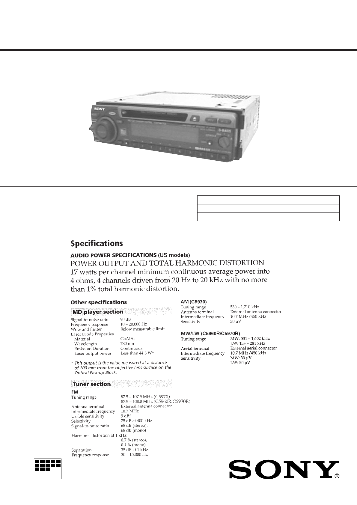
MDX-C5960R/C5970/C5970R
SERVICE MANUAL
Photo: MDX-C5960R
SPECIFICATIONS
German Model
MDX-C5960R
US Model
Canadian Model
E Model
MDX-C5970
AEP Model
UK Model
MDX-C5970R
Model Name Using Similar Mechanism MDX-C7900/C7900R
Base Mechanism Type MG-164N-138
Optical Pick-Up Name KMS-241B/J1NP
MICROFILM
– Continued on next page –
FM/AM (MW/LW) MINIDISC PLAYER
Page 2
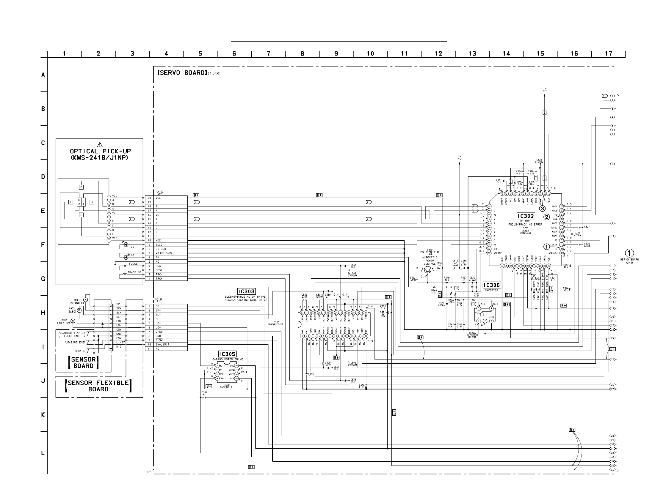
4-8. SCHEMATIC DIAGRAM – SERVO Board (1/3) –
• See page 55 for Waveforms. • See page 58 for IC Block Diagrams.
The components identified by mark ! or dotted
line with mark ! are critical for safety.
Replace only with part number specified.
Les composants identifiés par une marque ! sont
critiques pour la sécurité. Ne les remplacer que
par une piéce portant le numéro spécifié.
• Voltages and waveforms are dc with respect
to ground under no-signal conditions.
no mark : MD PLAY
: Impossible to measure
∗
MDX-C5960R/C5970/C5970R
(Page 35)
– 33 – – 34 –
Page 3
MDX-C5960R/C5970/C5970R
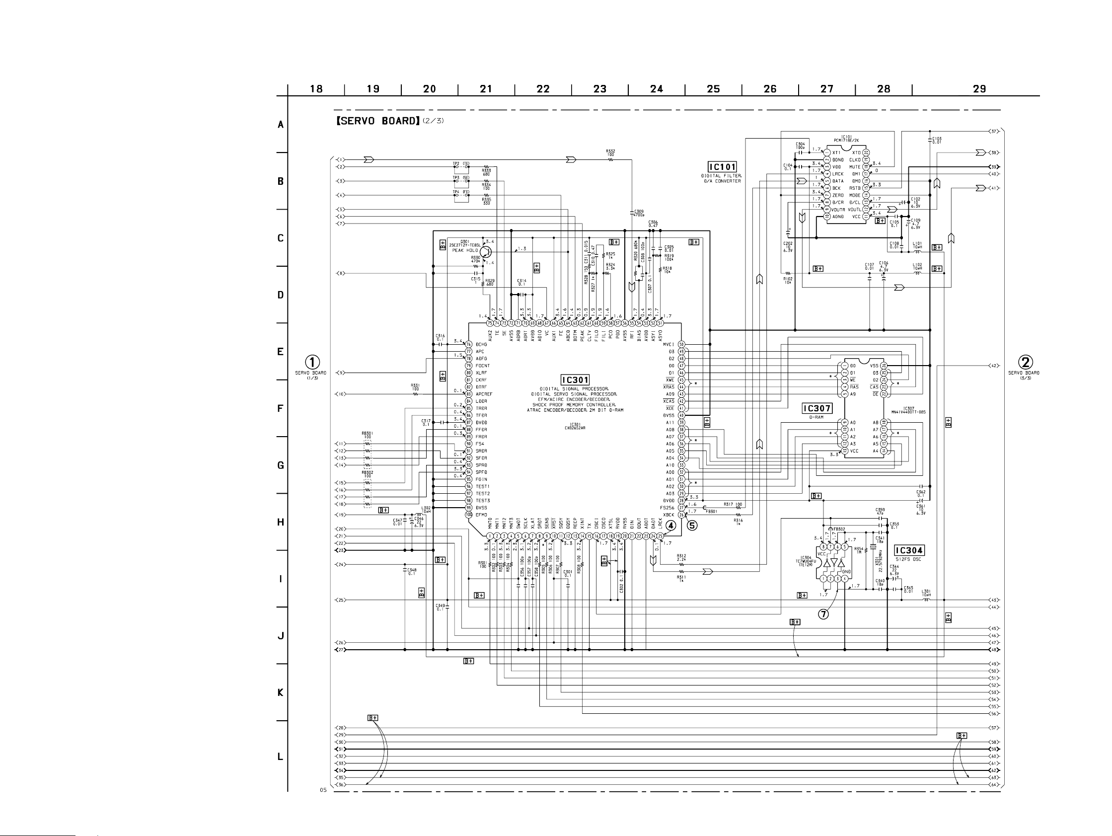
4-9. SCHEMATIC DIAGRAM – SERVO Board (2/3) – • See page 55 for Waveforms. • See page 57 for IC Block Diagrams.
(Page 34)
(Page 37)
• Voltages and waveforms are dc with respect to ground
under no-signal conditions.
no mark : MD PLAY
: Impossible to measure
∗
– 35 – – 36 –
Page 4
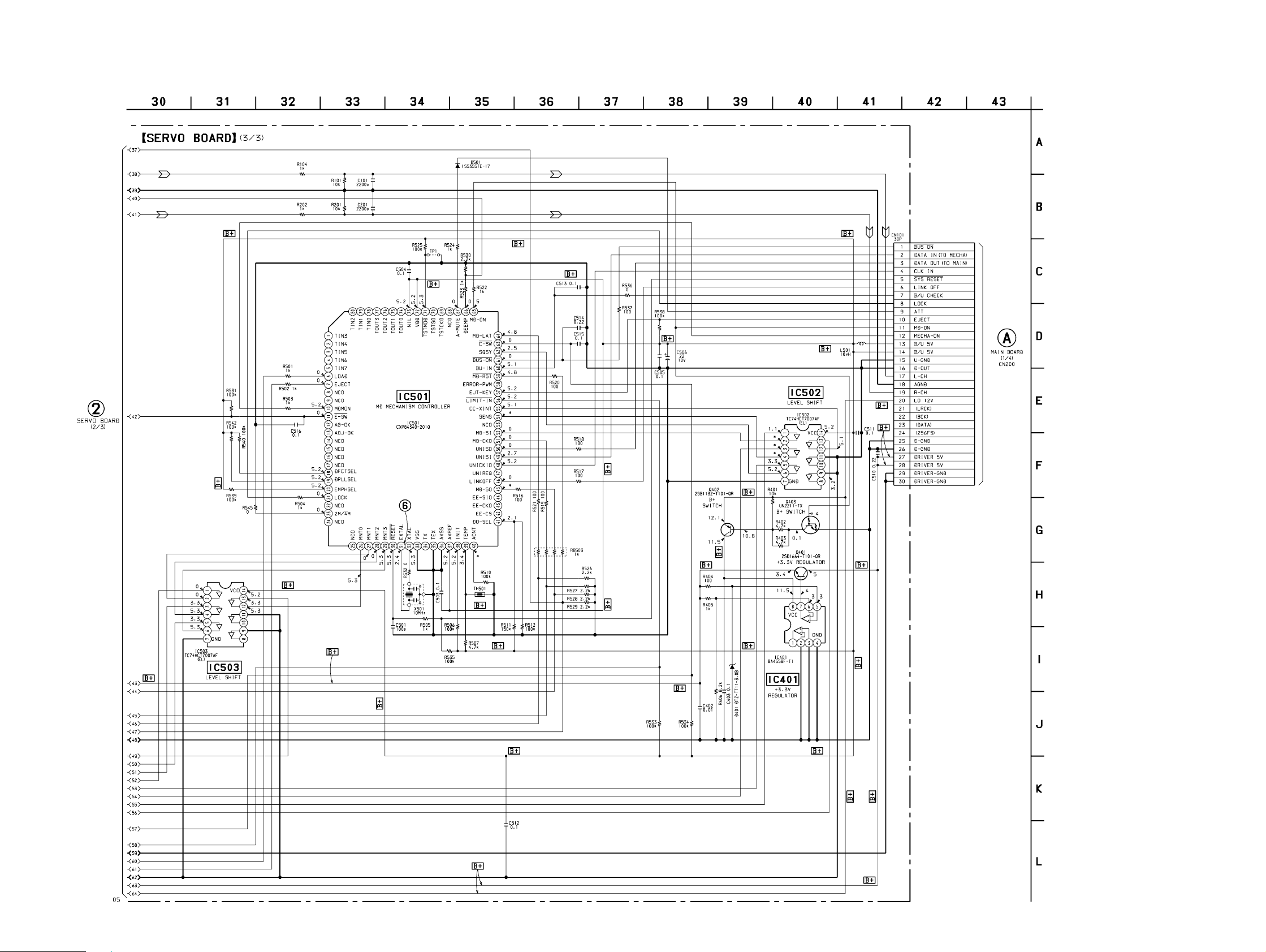
4-10. SCHEMATIC DIAGRAM – SERVO Board (3/3) – • See page 55 for Waveforms.
• Voltages and waveforms are dc with respect to ground
under no-signal conditions.
no mark : MD PLAY
: Impossible to measure
∗
MDX-C5960R/C5970/C5970R
(Page 36)
(Page 43)
– 37 –
– 38 –
Page 5
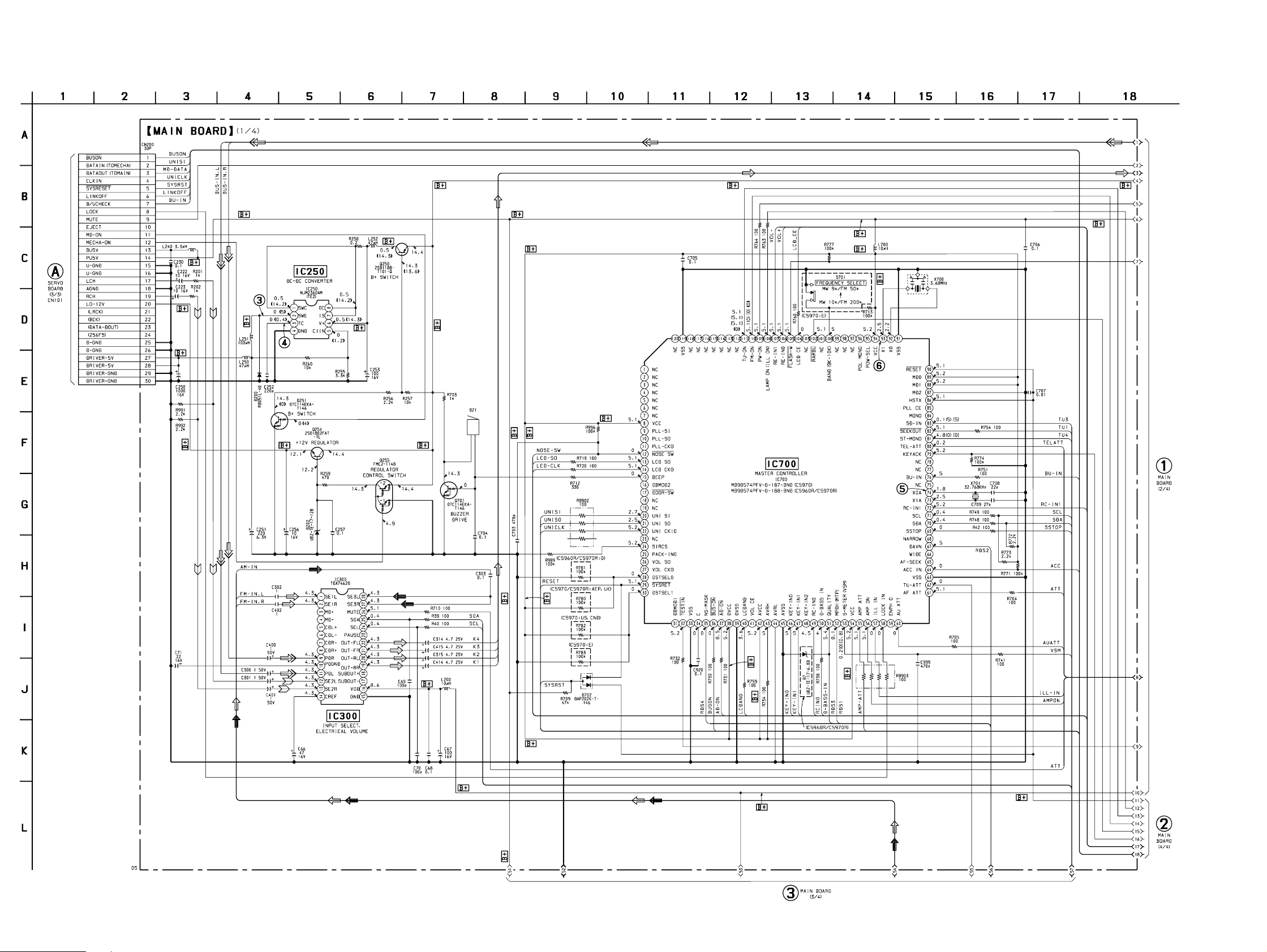
MDX-C5960R/C5970/C5970R
4-13. SCHEMATIC DIAGRAM – MAIN Board (1/4) – • See page 55 for Waveforms. • See page 60 for IC Block Diagrams.
(Page 38)
• Voltages and waveforms are dc with respect to ground
under no-signal (detuned) conditions.
no mark : FM
( ) : AM (MW)
[]: LW
〈〈 〉〉 : MD PLAY
(Page 45)
(Page 48)
– 43 – – 44 –
(Page 49)
Page 6
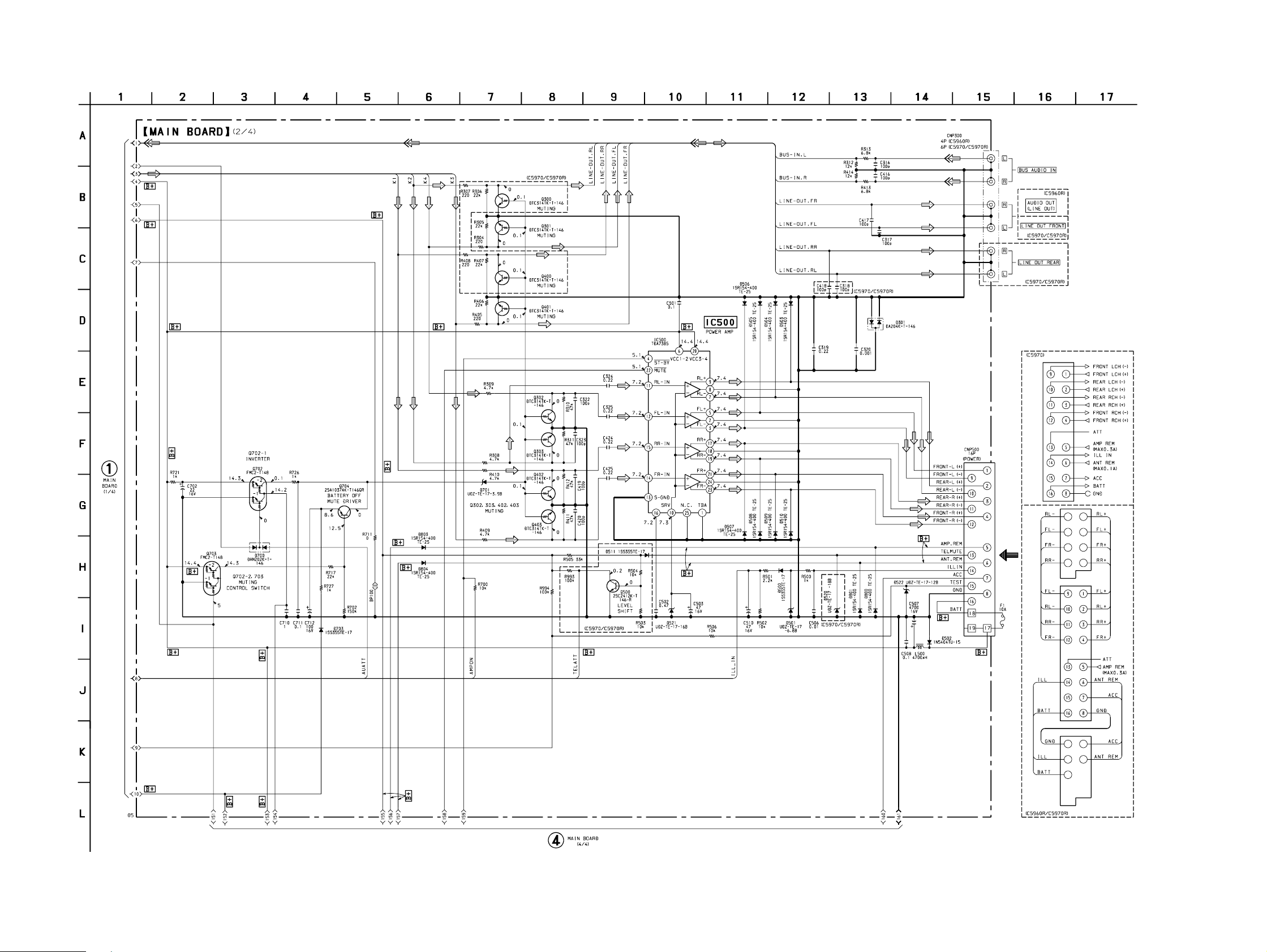
4-14. SCHEMATIC DIAGRAM – MAIN Board (2/4) –
MDX-C5960R/C5970/C5970R
(Page
44)
(Page 49)
• Voltages are dc with respect to ground under no-signal
(detuned) conditions.
no mark : FM
– 45 – – 46 –
Page 7
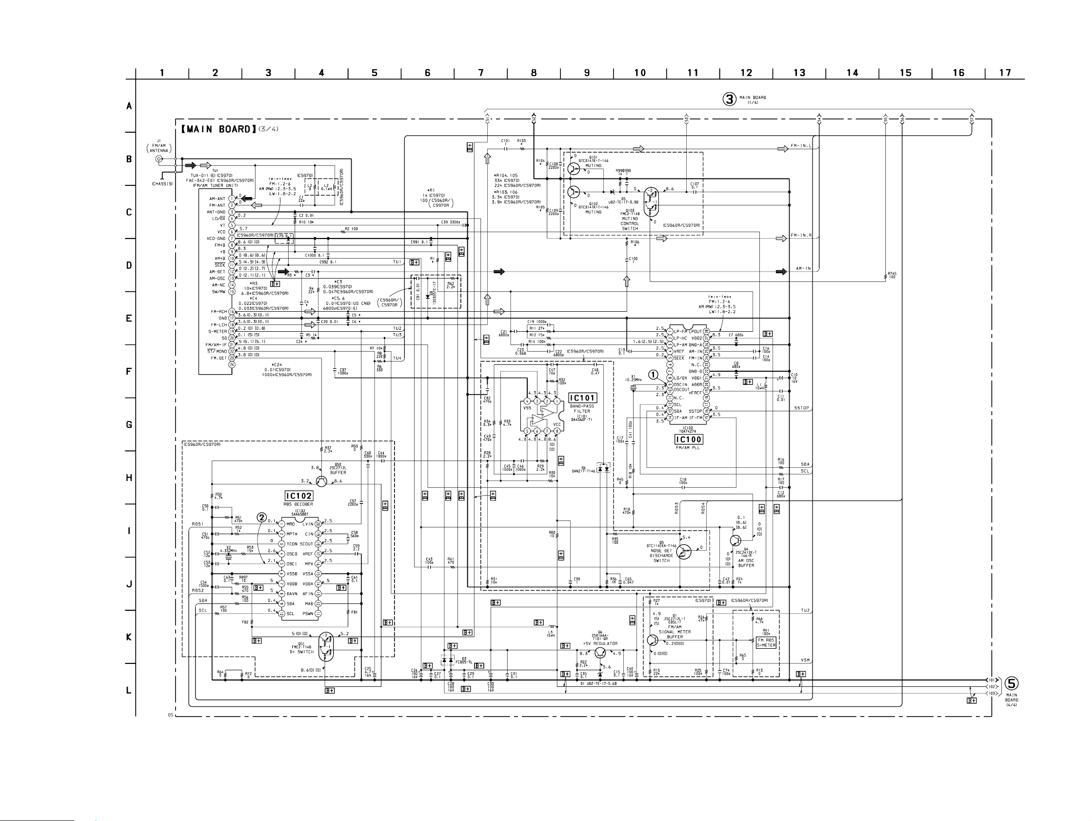
MDX-C5960R/C5970/C5970R
4-15. SCHEMATIC DIAGRAM – MAIN Board (3/4) – • See page 55 for Waveforms. • See page 60 for IC Block Diagrams.
(Page 44)
• Voltages and waveforms are dc with respect to ground
under no-signal (detuned) conditions.
no mark : FM
( ) : AM (MW)
[]: LW
– 47 – – 48 –
(Page 49)
Page 8
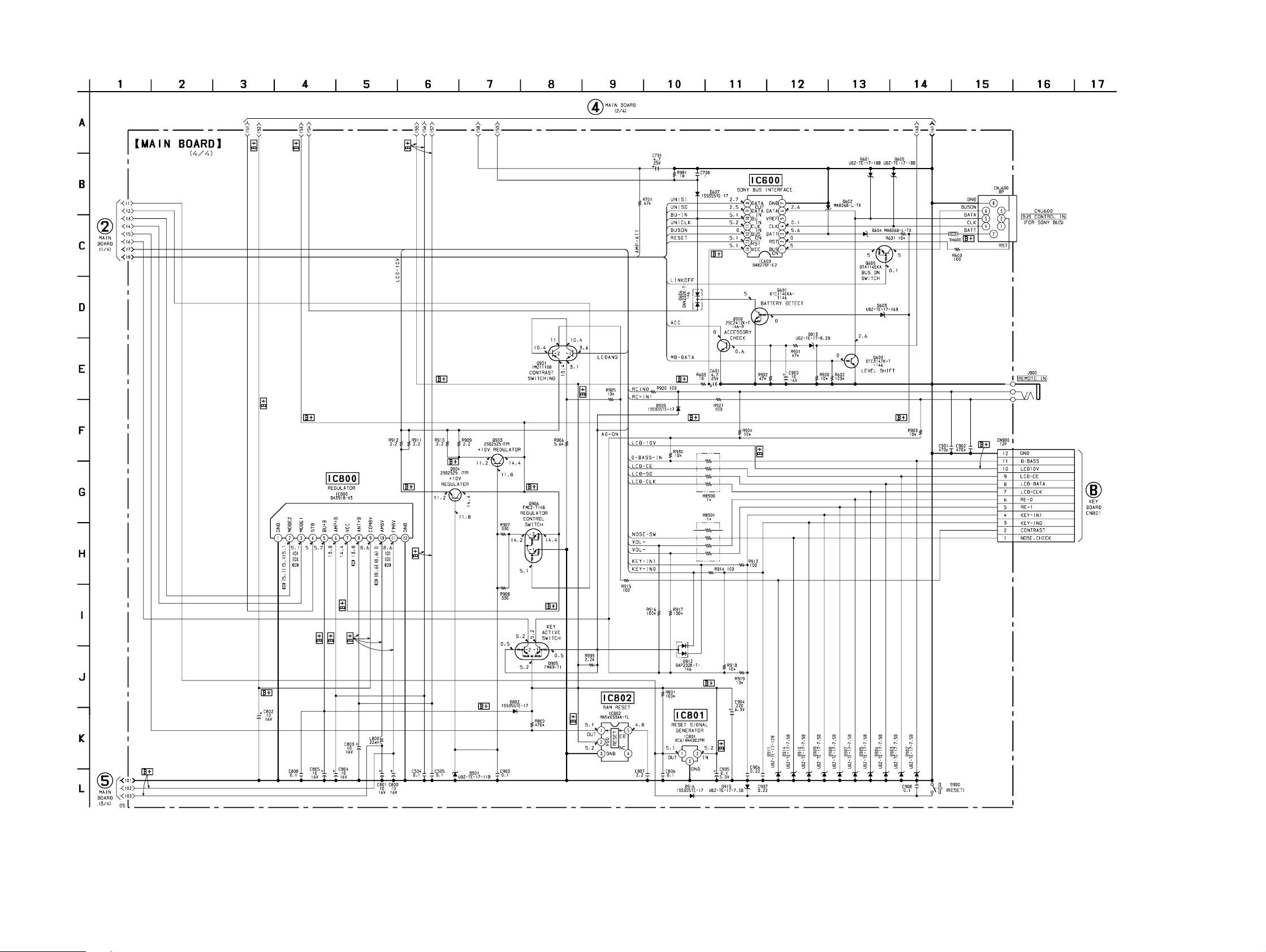
4-16. SCHEMATIC DIAGRAM – MAIN Board (4/4) – • See page 61 for IC Block Diagrams.
(Page
44)
MDX-C5960R/C5970/C5970R
(Page 45)
(Page 48)
(Page 53)
• Voltages are dc with respect to ground under no-signal
(detuned) conditions.
no mark : FM
( ) : AM (MW)
[]: LW
〈〈 〉〉 : MD PLAY
– 49 – – 50 –
Page 9

4-18. SCHEMATIC DIAGRAM – KEY Board – • See page 56 for Waveforms.
(Page 50)
MDX-C5960R/C5970/C5970R
– 53 – – 54 –
• Voltages and waveforms are dc with respect to ground
under no-signal (detuned) conditions.
no mark : FM
Page 10

• Wavef orms
– SERVO Board –
– MAIN Board –
– KEY Board –
1 IC302 @§ (TE) (MD PLAY Mode)
2 IC302 #¢ (FE) (MD PLAY Mode)
3 IC302 #• (RF) (MD PLAY Mode)
Approx.
0.5 Vp-p
Approx.
0.3 Vp-p
6 IC501 #¡ (EXTAL) (MD PLAY Mode)
2.7 Vp-p
0.1 µs
7 IC304 3 (IN) (MD PLAY Mode)
3.5 Vp-p
44 ns
1 IC100 9 (OSC IN) (FM/AM (MW) Mode)
2.7 Vp-p
94 ns
2 IC102 5 (OSC1) (FM Mode)
2.8 Vp-p
224 ns
3 IC250 2 SWE (MD PLAY Mode)
6 IC700 (£ (X1)
271 ns
5.8 Vp-p
1 IC801 @º (OSC IN)
2.8 Vp-p
3.5 µs
1.2 Vp-p
4 IC301 @∞ (LRCK) (MD PLAY Mode)
3.5 Vp-p
23 µs
5 IC301 @§ (XBCK) (MD PLAY Mode)
4.5 Vp-p
14.2 Vp-p
24 µs
4 IC250 3 TC (MD PLAY Mode)
1.1 Vp-p
12 µs
5 IC700 &¢ (XOA)
2.1 Vp-p
356 µs
30 µs
– 55 – – 56 –
Page 11

• IC Block Diagrams
– SERVO Board –
IC101 PCM1718E/2K
XTI
DGND
VDD
LRCIN
DIN
BCKIN
ZERO
D/C_R
VOUTR
AGND
1
2
3
4
5
6
7
8
9
10
INPUT
INTERFACE
DIGITAL
FILTER
NOISE SHAPER
5 LEVEL
DAC
LOWPASS
FILTER
CMOS
AMP
CONTROL
IC301 CXD2652AR
EFMO
DVSS
TEST3
TEST2
99 98 97 96 95 94 93
SUBCODE
CLOCK
MNT0
MNT1
MNT2
MNT3
SWDT
SCLK
XLAT
SRDT
SENS
XRST
SQSY
DQSY
RECP
XINT
OSCI
OSCO
XTSL
DVSS
DIN
DOUT
100
1
2
MONITOR
CONTROL
3
4
5
6
CPU I/F
7
8
9
10
11
PROCESSOR
12
13
14
15
TX
16
17
GENERATOR
18
19
NC
20
21
22
CLK
TEST1
EACH
BLOCK
EACH
BLOCK
MODE
CONTROL
5 LEVEL
DAC
LOWPASS
FILTER
CMOS
AMP
FGIN
SPINDLE
SERVO
ADIP
DECODER
EACH
BLOCK
SPFD
SPRD
DIGITAL
AUDIO
XTO
20
CLKO
19
MUTE
18
DM1
17
DM0
16
RSTB
15
FORMAT
14
D/C_L
13
VOUTL
12
VCC
11
SFDR91SRDR90FS489FRDR88FFDR87DVDD86TFDR85TRDR84LDDR83APCREF82DTRF81CKRF80XLRF79F0CNT78ADFG77APC76DCHG
92
PWM
SHOCK RESISTANT
MEMORY CONTROLLER
SAMPLING
I/F
RATE
CONVERTER
GENERATOR
SERVO
DSP
CONVERTER
AUTO
A/D
SEQUENCER
ANALOG
DECODER
ENCODER/
EFM/ACIRC
COMP
MUX
PLL
75
AUX2
74
TE
73
SE
72
AVSS
71
ADRB
70
ADRT
69
AVDD
68
ADIO
67
VC
66
AUX1
65
FE
64
ABCD
63
BOTM
62
PEAK
61
CLTV
60
FILO
59
FILI
58
PCO
57
PDO
56
AVSS
55
RFI
54
BIAS
53
AVDD
52
ASYI
51
ASYO
ADDT
DADT
LRCK
23
24
25
28
26
27
XBCK
DVDD
FS256
ATRAC
ENCODER/DECODER
ADDRESS/DATA BUS A00 - A11, D0 - D3
40
39
A1138A0837A0736A0635A0534A0433A1032A0031A0130A0229A03
41
DVSS
XOE
50
44
43
42
A09
XWE
XCAS
XRAS
49D348D247D046D145
MVCI
– 57 –
Page 12

IC302 CXA2523R
MORFO47MORFI46RFO45OPN
48
–
+
RFA1
+
–
1I
2J
CVB
3VC
4A
IVR
5B
IVR
6C
IVR
7D
IVR
8E
IVR
9F
IVR
GSW IV
+
–
+
–
+
–
+
–
+
–
+
–
+
–
RFA2
–
–
–
–
–
–
–
AA
BB
CC
DD
EE
FF
1
2
1
2
GRVA
HLPT
CFST
GRV
+
–
+
–
FBAL
OPO43ADDC42COMPP41COMPO40AGCI39RF AGC38RF37PEAK
44
USROP
EE'
–1
–2
–2
–1
+
+
+
+
+
+
–
–
–
–
+
+
FF'
+
–
BPF3T
PTGR
ABCDA
FEA
BPF22
WBL
ATA
WBL
–
+
–
+
EFB TESW
RF AGC EQ
USRC
PEAK
BOTTOM
WBL
ADIP
PTGR
PEAK3T
P-P
PBH
AGC
WBL
3T
EQ
3T
3T WBL
DET
–1
–2
–1
–2
DET
TEMP
EQ
BPFC
SEA
TEA
VI CONV
TG
TG
36
BOTM
35
ABCD
34
FE
33
AUX
32 ADFG
31 ADAGC
30 ADIN
29 ADFM
28 SE
27 CSLED
26 TE
25 WBLADJ
15
AUXSW
TEMPR
COMMAND
SCRI - PARA
DECODE
17
16
SCLK
SWDT
BGR
VREF
24
23
22
21
20
19
18
XLAT
XSTBY
F0CNT
VREF
EQADJ
3TADJ
VCC
10PD
11APC
12APCREF
+
–
+
–
14
13
GND
TEMPI
– 58 –
Page 13

IC303 BH6511FS-E2
CAPA–
CAPA+
IN2R
IN2F
VM2
OUT2F
PGND2
OUT2R
VM12
OUT1R
PGND1
OUT1F
VM1
32 31 30 29 28 27 26 25 24 23 22 21 20 19 18 17
IN4F
AMP
AMP
VM4
INTERFACE
CHARGE
PUMP.
OSC
INTERFACE
1 2 3 4 5 6 7 8 9 10 11 12 13 14 15 16
VG
GND
IN4R
OUT4F
PGND4
AMP
OUT4R
VM34
AMP
OUT3R
PGND3
AMP
AMPAMPAMP
OUT3F
PREDRIVEPREDRIVE
PREDRIVEPREDRIVE
VM3
IC305 BA6287F
1
OUT1
VM
2
8
GND
7
OUT2
IN1F
INTERFACE
INTERFACE
IN3F
IN1R
IN3R
V
PSB
DD
V
DD
PSB
DRIVER DRIVER
TSD
3
VCC
POWER
SAVE
4
FIN
CONTROL LOGIC
IC307 MN41V4400TT-08S
1
D1
2
D2
XWE
3
4
XRAS
NC
5
NC
6
7
NC
A9
8
A0
9
10
A1
A2
11
12
A3
A0–A9
A0–A9
ADDRESS BUFFER
CLOCK OSC
COLUMN DECODER
SENSE REFRESH AMP
INPUT/OUTPUT CONTROL SWITCH
MEMORY CELL
(4194204 BIT)
ROW DECODER
6
VREF
5
RIN
GND
26
D4
25
24
D3
XCAS
23
XOE
22
BUFFER
(4) INPUT
BUFFER
(4) OUTPUT
21
NC
20
NC
NC
19
A8
18
A7
17
16
A6
15
A5
1413
A4VDD
– 59 –
Page 14

– MAIN Board –
IC100 TDA7427AD
LP OUT
11 BIT
PROGRAMMABLE
COUNTER
SWITCH
OUT
INLOCK
CHARGE
PUMP
DETECTOR
PARATOR
+
–
SWITCH
LP1/LP2
3 41 2 785 6 11 129
VREF
LP HC
LP FM
LP AM
PHASE
COM-
SWITCH
SWM/DIR
5 BIT
PROGRAMMABLE
COUNTER
PRE
COUNTER
SWITCH
SWM/DIR
16 BIT
PROGRAMMABLE
COUNTER
TEST
LOGIC
PORT
EXTENSION
DOUT3
DOUT4
DOUT5
DOUT6
FM/AM
SWITCH
TIMER
14 BIT
PROGRAMMABLE
COUNTER
REFERENCE
OSCILLATOR
10
OSCIN
OSCOUT
VDD2
AM IN
GND-AM
NC
NC
FM IN
POWER ON RESET
CONTROL
11 – 21 BIT
PROGRAMMABLE
COUNTER
GND-SIG
SUPPLY &
VDD1
ADDR
IIC BUS
INTERFACE
SCL
DOUT1/INLOCK
HFREF
SSTOP
DOUT2
FM/AM
SWITCH
13 14
SDA
IF FM
1516171819202122232425262728
IF AM
IC102 SAA6588T-118 (MDX-C5960R/C5970R)
6
VSSD
CLOCK
DATA
VDDD
VREF
17
87
DAVN
MPX
POWER SUPPLY
SIGNAL QUALITY
DECODER
445
INTERFACE
REGISTER
VSSA
15
& RESET
LVIN
20
MULTI
PATH
DETECTOR
2
1
MRO
MPTH
CIN
19
CLOCKED
COMPARATOR
RDS/RDBS
DEMODULATOR
TEST
CONTROL
3
TCON
SCOUT
18
BAND-PASS FILTER
OSCILLATOR
& CLOCK
4 5
OSCO
57kHz
8th ORDER
RDS/RDBS
DECODER
OSCI
VDDA
14
CLOCK
DATA
IIC BUS SLAVE
TRANSCEIVER
9 10
1316
SDA
AFIN
SCL
PAUSE
DETECTOR
IC250 NJM2360AM (TE2)
MAD
PSWN
11
12
Q2
1CS
Q1
2ES
3CT
4GND
VREF
1.25V
QS
R
+
–
CT OSC
COMP
Ipk
8CD
7SI
6V+
5 INVIN
– 60 –
Page 15

IC300 TDA7462D013TR
SE3L
SE3R
MUTE
SDA
SCL
PAUSE
OUT FL
OUT FR
OUT RL
OUT RR
SUBOUT+
SUBOUT–
VDD
GND
CREF
SE1L
SE1R
MD+
MD–
CDL+
CDL–
CDR–
CDR+
PDR
PDGND
PDL
SE2L
SE2R
INPUT
GAIN &
AUTO
ZERO
PAUSE
DETECT
INPUT MULTIPLEXER &
MIXING STAGE
REAR SIDE
SELECTOR
FRONT SIDE
SELECTOR
LOUDNESS
CONTROL
CIRCUIT
INPUT
GAIN
BEEP
LOUDNESS
CONTROL
CIRCUIT
SOFT
MUTE
VOLUME
CONTROL
CIRCUIT
COMPANDER
TREBLE/
BASS
CONTROL
CIRCUIT
SUBWOOFER
OUT
FADER
SUBWOOFER
LP
IIC
BUS
DIGITAL CONTROL CIRCUIT
POWER
SUPPLY
FRONT
FADER
FRONT
FADER
REAR
FADER
REAR
FADER
VOICE BANDPASS
HP LP
SDA
SCL
1
2
3
4
5
6
7
8
9
10
11
12
13
14
15
16
17
18
19
20
21
22
23
24
25
26
27
28
IC600 BA8270F-E2
BUS ON
SWITCH
RESET
SWITCH
BATTERY
SWITCH
BUS ON
1
2
RST
BATT
3
4
CLK
5
VREF
6
DATA
GND
7 8
14
13
12
11
10
9
VCC
RST
BUS ON
CLK IN
BU IN
DATA IN
DATA OUT
IC800 BA3918-V3
1
NC
2 3
MODE2
4
STB
MODE1
–
+
– 61 –
REGULATOR
OVER VOLTAGE
PROTECT
5 6 7 8 9 10 1211
VDD
AMP
VCC
ANT
COM
–
+
AM
–
+
–
+
FM
GND
Page 16

4-19. IC PIN FUNCTION DESCRIPTION
• SERVO BOARD IC301 CXD2652AR
(DIGITAL SIGNAL PROCESSOR, DIGITAL SERVO PROCESSOR, EFM/ACIRC ENCODER/DECODER,
SHOCK PROOF MEMORY CONTROLLER, ATRAC ENCODER/DECODER, 2M BIT D-RAM)
Pin No. Pin Name I/O Function
1 MNT0 O
2 MNT1 O
3 MNT2 O
4 MNT3 O
5 SWDT I
6 SCLK I
7 XLAT I
8 SRDT O (3)
9 SENS O (3)
10 XRST I Reset signal input from the MD mechanism controller (IC501) “L”: reset
11
SQSY O
Focus OK signal output to the MD mechanism controller (IC501)
“H” is output when focus is on (“L”: NG)
Track jump detection signal output to the MD mechanism controller (IC501)
Busy monitor signal output to the MD mechanism controller (IC501)
Spindle servo lock status monitor signal output to the MD mechanism controller (IC501)
Writing serial data signal input from the MD mechanism controller (IC501)
Serial data transfer clock signal input from the MD mechanism controller (IC501)
Serial data latch pulse signal input from the MD mechanism controller (IC501)
Reading serial data signal output to the MD mechanism controller (IC501)
Internal status (SENSE) output to the MD mechanism controller (IC501)
Subcode Q sync (SCOR) output to the MD mechanism controller (IC501)
“L” is output every 13.3 msec Almost all, “H” is output
12
13 RECP I
14 XINT O Interrupt status output to the MD mechanism controller (IC501)
15 TX I
16 OSCI I System clock signal (512Fs=22.5792 MHz) input from the oscillator circuit
17 OSCO O System clock signal (512Fs=22.5792 MHz) output terminal Not used (open)
18 XTSL I
19 RVDD — Power supply terminal (+3.3V) (digital system)
20 RVSS — Ground terminal (digital system)
21
22
23
24
25
26
27 FS256 O
28 DVDD — Power supply terminal (+3.3V) (digital system)
29 to 32
33
34 to 38
39
40 DVSS — Ground terminal (digital system)
41 XOE O Output enable signal output to the D-RAM (IC307) “L” active
42 XCAS O Column address strobe signal output to the D-RAM (IC307) “L” active
43 A09 O Address signal output to the D-RAM (IC307)
44 XRAS O Row address strobe signal output to the D-RAM (IC307) “L” active
45 XWE O Write enable signal output to the D-RAM (IC307) “L” active
DQSY O
DIN I Digital audio signal input terminal when recording mode Not used (fixed at “L”)
DOUT O Digital audio signal output terminal when playback mode Not used (open)
ADDT I Recording data input terminal Not used (fixed at “L”)
DADT O Playback data output to the PCM1718E (IC101)
LRCK O L/R sampling clock signal (44.1 kHz) output to the PCM1718E (IC101)
XBCK O Bit clock signal (2.8224 MHz) output to the PCM1718E (IC101)
A03 to A00 O Address signal output to the D-RAM (IC307)
A10 O
A04 to A08 O Address signal output to the D-RAM (IC307)
A11 O
Digital In U-bit CD format subcode Q sync (SCOR) output terminal
“L” is output every 13.3 msec Almost all, “H” is output Not used (open)
Laser power selection signal input terminal
“L”: playback mode, “H”: recording mode (fixed at “L” in this set)
Recording data output enable signal input terminal
Writing data transmission timing input (Also serves as the magnetic head on/off output)
Not used (fixed at “L”)
Input terminal for the system clock frequency setting
“L”: 45.1584 MHz, “H”: 22.5792 MHz (fixed at “H” in this set)
Clock signal (11.2896 MHz) output to the PCM1718E (IC101)
Address signal output to the external D-RAM Not used (open)
Address signal output to the external D-RAM Not used (open)
– 62 –
Page 17

Pin No. Pin Name I/O Function
46 D1 I/O
47 D0 I/O
48 D2 I/O
Two-way data bus with the D-RAM (IC307)
49 D3 I/O
50 MVCI I Digital in PLL oscillation input from the external VCO Not used (fixed at “L”)
51 ASYO O Playback EFM full-swing output terminal
52 ASYI I (A) Playback EFM asymmetry comparator voltage input terminal
53 AVDD — Power supply terminal (+3.3V) (analog system)
54 BIAS I (A) Playback EFM asymmetry circuit constant current input terminal
55 RFI I (A) Playback EFM RF signal input from the CXA2523R (IC302)
56 AVSS — Ground terminal (analog system)
57 PDO O (3) Phase comparison output for clock playback analog PLL of the playback EFM Not used (open)
58 PCO O (3) Phase comparison output for master clock of the recording/playback EFM master PLL
59 FILI I (A) Filter input for master clock of the recording/playback master PLL
60 FILO O (A) Filter output for master clock of the recording/playback master PLL
61 CLTV I (A) Internal VCO control voltage input of the recording/playback master PLL
62 PEAK I (A) Light amount signal (RF/ABCD) peak hold input from the CXA2523R (IC302)
63 BOTM I (A) Light amount signal (RF/ABCD) bottom hold input from the CXA2523R (IC302)
64 ABCD I (A) Light amount signal (ABCD) input from the CXA2523R (IC302)
65 FE I (A) Focus error signal input from the CXA2523R (IC302)
66 AUX1 I (A) Auxiliary signal (I
3 signal/temperature signal) input terminal Not used (fixed at “H”)
67 VC I (A) Middle point voltage (+1.65V) input from the CXA2523R (IC302)
68 ADIO O (A) Monitor output of the A/D converter input signal Not used (open)
69 AVDD — Power supply terminal (+3.3V) (analog system)
70 ADRT I (A) A/D converter operational range upper limit voltage input terminal (fixed at “H” in this set)
71 ADRB I (A) A/D converter operational range lower limit voltage input terminal (fixed at “L” in this set)
72 AVSS — Ground terminal (analog system)
73 SE I (A) Sled error signal input from the CXA2523R (IC302)
74 TE I (A) Tracking error signal input from the CXA2523R (IC302)
75 AUX2 I (A) Auxiliary signal input terminal Light amount signal input from the CXA2523R (IC302)
76 DCHG I (A) Connected to the +3.3V power supply
77 APC I (A) Error signal input for the laser automatic power control Not used (fixed at “L”)
78 ADFG I ADIP duplex FM signal (22.05 kHz ± 1 kHz) input from the CXA2523R (IC302)
79 F0CNT O Filter f0 control signal output terminal Not used (open)
80 XLRF O Serial data latch pulse signal output terminal Not used (open)
81 CKRF O Serial data transfer clock signal output terminal Not used (open)
82 DTRF O Writing serial data output terminal Not used (open)
83 APCREF O
Control signal output to the reference voltage generator circuit for the laser automatic power
control
84 LDDR O PWM signal output for the laser automatic power control Not used (open)
85 TRDR O Tracking servo drive PWM signal (–) output to the BH6511FS (IC303)
86 TFDR O Tracking servo drive PWM signal (+) output to the BH6511FS (IC303)
87 DVDD — Power supply terminal (+3.3V) (digital system)
88 FFDR O Focus servo drive PWM signal (+) output to the BH6511FS (IC303)
89 FRDR O Focus servo drive PWM signal (–) output to the BH6511FS (IC303)
90 FS4 O Clock signal (176.4 kHz) output terminal (X’tal system) Not used (open)
91 SRDR O Sled servo drive PWM signal (–) output to the BH6511FS (IC303)
– 63 –
Page 18

Pin No. Pin Name I/O Function
92 SFDR O Sled servo drive PWM signal (+) output to the BH6511FS (IC303)
93 SPRD O Spindle servo drive PWM signal (–) output to the BH6511FS (IC303)
94 SPFD O Spindle servo drive PWM signal (+) output to the BH6511FS (IC303)
95
96
97
98
99 DVSS — Ground terminal (digital system)
100 EFMO O EFM signal output terminal when recording mode Not used (open)
* I (A) for analog input, O (3) for 3-state output, and O (A) for analog output in the column I/O.
FGIN I Not used (fixed at “L”)
TEST1 I
TEST2 I Input terminal for the test (fixed at “L”)
TEST3 I
– 64 –
Page 19

• SERVO BOARD IC302 CXA2523R (RF AMP, FOCUS/TRACKING ERROR AMP)
Pin No. Pin Name I/O Function
1II
2JI
3VCO
4 to 9 A to F I
10 PD I
11 APC O
12 APCREF I
13 GND —
14 TEMPI I
15
TEMPR O
16 SWDT I
17 SCLK I
18 XLAT I
19 XSTBY I
20 F0CNT I
21 VREF O
22 EQADJ I
23 3TADJ I
24 VCC —
25 WBLADJ I
26 TE O
27 CSLED I
28 SE O
29 ADFM O
30 ADIN I
31 ADAGC I
32 ADFG O
33 AUX O
34 FE O
35 ABCD O
36 BOTM O
37 PEAK O
38 RF O
39 RFAGC I
40 AGCI I
41 COMPO O
42 COMPP I
43 ADDC I
44 OPO O
45 OPN I
46 RFO O
47 MORFI I
48 MORFO O
I-V converted RF signal I input from the optical pick-up block detector
I-V converted RF signal J input from the optical pick-up block detector
Middle point voltage (+1.65V) generation output terminal
Signal input from the optical pick-up detector
Light amount monitor input from the optical pick-up block laser diode
Laser amplifier output terminal to the automatic power control circuit
Reference voltage input terminal for setting laser power
Ground terminal
Connected to the temperature sensor Not used (open)
Output terminal for a temperature sensor reference voltage Not used (open)
Writing serial data input from the MD mechanism controller (IC501)
Serial data transfer clock signal input from the MD mechanism controller (IC501)
Serial data latch pulse signal input from the MD mechanism controller (IC501)
Standby signal input terminal “L”: standby (fixed at “H” in this set)
Center frequency control voltage input terminal of internal circuit (BPF22, BPF3T, EQ) input
terminal
Reference voltage output terminal Not used (open)
Center frequency setting terminal for the internal circuit (EQ)
Center frequency setting terminal for the internal circuit (BPF3T)
Power supply terminal (+3.3V)
Center frequency setting terminal for the internal circuit (BPF22)
Tracking error signal output to the CXD2652AR (IC301)
Connected to the external capacitor for low-pass filter of the sled error signal
Sled error signal output to the CXD2652AR (IC301)
FM signal output of the ADIP
Receives a ADIP FM signal in AC coupling
Connected to the external capacitor for ADIP AGC
ADIP duplex signal (22.05 kHz ± 1 kHz) output to the CXD2652AR (IC301)
3
Auxiliary signal (I
signal/temperature signal) output terminal Not used (open)
Focus error signal output to the CXD2652AR (IC301)
Light amount signal (ABCD) output to the CXD2652AR (IC301)
Light amount signal (RF/ABCD) bottom hold output to the CXD2652AR (IC301)
Light amount signal (RF/ABCD) peak hold output to the CXD2652AR (IC301)
Playback EFM RF signal output to the CXD2652AR (IC301)
Connected to the external capacitor for RF auto gain control circuit
Receives a RF signal in AC coupling
User comparator output terminal Not used (open)
User comparator input terminal Not used (fixed at “L”)
Connected to the external capacitor for cutting the low band of the ADIP amplifier
User operational amplifier output terminal Not used (open)
User operational amplifier inversion input terminal Not used (fixed at “L”)
RF signal output terminal
Receives a MO RF signal in AC coupling
MO RF signal output terminal
– 65 –
Page 20

• SERVO BOARD IC501 CXP84340-201Q (MD MECHANISM CONTROLLER)
Pin No. Pin Name I/O Function
1 to 5 TIN3 to TIN7 I/O
6 LOAD
7 EJECT O
8, 9 NCO O
10 MDMON O
Input of the 4×8 matrix test keys (“L” is always output, except in test mode) Not used (open)
O Loading motor control signal output to the motor driver (IC305) “H” active *1
Loading motor control signal output to the motor driver (IC305) “H” active *1
Not used (open)
Power supply on/off control signal output of the MD mechanism deck section main power supply
and loading motor drive (IC305) power supply “H”: power on
11 E-SW I
12 AG-OK O
13 ADJ-OK O
14 to 17 NCO O
18 DFCTSEL I
19 DPLLSEL I
20 EMPHSEL I
21 LOCK O
22 NCO O
23 2M/4M I
24, 25 NCO O
26
27 MNT1 I
28 MNT2 I
29 MNT3 I
30 RESET I
31 EXTAL
32 XTAL
33 VSS
34 TX
35 TEX
36 AVSS
37 AVREF
38 INIT
39 TEMP
40 ACNT
41 DO-SEL
42 EE-CS
43 EE-CKO
44 EE-SIO I/O
45 MD-SO O
46 LINKOFF O
MNT0
Inputs the disc loading completion detect switch detection signal
“L”: When completed of the disc loading operation
Output of aging status in test mode “L”: under aging, “H”: aging completed Not used (open)
Output of status when aging completed in test mode “L”: aging NG, “H”: aging OK
Not used (open)
Not used (open)
Select whether defect function is used for the CXD2652AR (IC301)
“L”: used this function , “H”: not used this function (fixed at “H” in this set)
Select whether digital PLL function is used for the CXD2652AR (IC301)
“L”: used this function , “H”: not used this function (fixed at “H” in this set)
Select whether emphasis signal output from pin or unilink data
“L”: outputs from both pin and unilink data, “H”: output from pin only (fixed at “H” in this set)
Mini-disc lock detection signal output to the master controller (IC700) “H”: lock
Not used (open)
Select whether D-RAM capacitance 2M bit or 4M bit “L”: 4M bit (external D-RAM) , “H”: 2M
bit (internal D-RAM of CXD2652AR) (fixed at “L” in this set)
Not used (open)
Focus OK signal input from the CXD2652AR (IC301)
I
“H” is input when focus is on (“L”: NG)
Track jump detection signal input from the CXD2652AR (IC301)
Busy monitor signal input from the CXD2652AR (IC301)
Spindle servo lock status monitor signal input from the CXD2652AR (IC301)
System reset signal input from the master controller (IC700), reset signal generator (IC801) and
reset switch (S900) “L”: reset For several hundreds msec. after the power supply rises, “L” is
input, then it changes to “H”
O Main system clock output terminal (10 MHz)
I Main system clock input terminal (10 MHz)
— Ground terminal
O Sub system clock output terminal (32.768 kHz) Not used (open)
I Sub system clock input terminal (32.768 kHz) Not used (fixed at “L”)
— Ground terminal (for A/D converter)
I Reference voltage input terminal (+5V) (for A/D converter)
I Initial reset signal input terminal (A/D input) (fixed at “H”)
I Temperature sensor (TH501) input terminal (A/D input)
Select the number of load/eject aging times (A/D input)
I
0H – 54H (30 times), 55H – OA9H (20 times), OAAH – OFFH (10 times)
I Select the digital output bits (A/D input)
O Chip select signal output to the external EEPROM device Not used (open)
O Serial data transfer clock signal output to the external EEPROM device Not used (open)
Two way data bus with the external EEPROM device Not used (open)
Writing serial data signal output to the CXD2652AR (IC301) and CXA2523R (IC302)
Unilink on/off control signal output for the SONY bus “L”: link on, “H”: link off
– 66 –
Page 21

Pin No. Pin Name I/O Function
n
47 UNIREQ O
48 UNICKIO I/O
49 UNISI I
50 UNISO O
51 MD-CKO O
52 MD-SI I
53 NCO O
54 SENS I
55 CC-XINT
56 LIMIT-IN
57 EJT-KEY I
58 ERROR-PWM O
59 MD-RST O
Data request signal output terminal (for SONY bus) “H”: request on Not used (open)
Serial clock signal input from the master controller (IC700) or serial clock signal output to the
SONY bus interface (IC600) and master controller (IC700) (for SONY bus)
Serial data input from the SONY bus interface (IC600)
Serial data output to the SONY bus interface (IC600)
Serial data transfer clock signal output to the CXD2652AR (IC301) and CXA2523R (IC302)
Reading serial data signal input from the CXD2652AR (IC301)
Not used (open)
Internal status (SENSE) input from the CXD2652AR (IC301)
I Interrupt status input from the CXD2652AR (IC301)
Detection input from the sled limit-in detect switch
I
The optical pick-up is inner position when “L”
Eject request signal input terminal “L”: eject on Not used (fixed at “H”)
PWM error monitor output terminal (C1and ATER is output when test mode) Not used (open)
Reset signal output to the PCM1718E (IC101), CXD2652AR (IC301) and BH6511FS (IC303)
“L”: reset
60 BU-IN I
61 BUS-ON I
62 SQSY
63 C-SW I
64 MD-LAT O
65 MD-ON O
66 DEEMP O
67 A-MUTE O
68 NCO O
69 TSTCKO O
70 TSTSO O
71 TSTMOD I
72 VCC —
73 NIL I
74 to 77
78 to 80 TIN0 to TIN2 I/O
TOUT0 to TOUT3
O
Battery detect signal input from the SONY bus interface (IC600) and battery check circuit
“H”: battery on
SONY bus on/off control signal input from the master controller (IC700) “L”: bus on
Subcode Q sync (SCOR) input from the CXD2652AR (IC301)
I
“L” is input every 13.3 msec Almost all, “H” is input
Inputs the disc loading start or disc eject completion detect switch detection signal
“L”: When start or eject completed of the disc loading operation
Serial data latch pulse signal output to the CXD2652AR (IC301) and CXA2523R (IC302)
Power supply on/off control signal output of the MD mechanism deck section main power supply
“H”: power on
Emphasis on/off control signal output to the PCM1718E (IC101) “H”: emphasis on
Audio muting on/off control signal output terminal
Not used (open)
Output of clock signal for the test mode display Not used (open)
Output of data for the test mode display Not used (open)
Setting terminal for the test mode “L”: test mode, “H”: normal mode
Power supply terminal (+5V)
Not used (fixed at “H”)
Output of the 4×8 matrix test keys Not used (open)
Input of the 4×8 matrix test keys (“L” is always output, except in test mode) Not used (open)
*1 Loading motor (M903) control
Operatio
Terminal
LOAD (pin 6)
EJECT (pin 7)
IN OUT BRAKE STOP
“H” “L” “H” “L”
“L” “H” “H” “L”
– 67 –
Page 22

MAIN BOARD IC700 (MASTER CONTROLLER)
•
MB90574PFV-G-188-BND (MDX-C5960R/C5970R) MB90574PFV-G-187-BND (MDX-C5970)
Pin No. Pin Name I/O Function
1 to 7 NC O
8 VCC —
9 PLL SI I
10 PLL SO O
11 PLL CKO O
12 NOSE-SW I
13 LCD SO
14 LCD CKO
15
16 DBMOD2 O
17 DOOR-SW I
18, 19 NC O
20 UNI SI
21 UNI SO
22 UNI CKIO
23 NC O
24
25 PACK-IND
26 VOL SO
27 VOL CKO
28 DSTSEL0 I
29 SYSRST O
30 DSTSEL1 I
31 DBMOD1 O
32 TESTIN
33
34 C —
35 NS-MASK O
36 BUS- ON
37 AD-ON
38 DVCC —
39 DVSS —
40 LCDANG
41 VOL CE
42 AVCC
BEEP O Beep sound drive signal output terminal
SIRCS
VSS
Not used (open)
Power supply terminal (+5V)
PLL serial data input terminal Not used (open)
PLL serial data output terminal Not used (open)
PLL serial data transfer clock signal output terminal Not used (open)
Front panel block remove/attach detection signal input terminal
“L”: front panel is attached
O Serial data output to the liquid crystal display driver (IC801)
O Serial data transfer clock signal output to the liquid crystal display driver (IC801)
D-BASS mode control signal output terminal Not used (open)
Front panel open/close detection signal input “L” is input when the front panel is closed
Not used (open)
Not used (open)
I Serial data input from the SONY bus interface (IC600)
O Serial data output to the SONY bus interface (IC600)
Serial clock signal output to the MD mechanism controller (IC501) and SONY bus interface
I/O
(IC600) or serial clock signal input from the MD mechanism controller (IC501) (for SONY bus)
Not used (open)
I
Sircs remote control signal input terminal Not used (fixed at “L”)
LED drive signal output of the MD disc slot illumination and 6 indicator “H”: LED on
O
“H” is output to turn on LED when front panel is opened Not used (open)
O Serial data output for the electrical volume Not used (open)
O Serial data transfer clock signal output for the electrical volume Not used (open)
Destination setting terminal
(Except German models: fixed at “H”, German model: fixed at “L”)
System reset signal output to the MD mechanism controller (IC501) and SONY bus interface
(IC600) “L”: reset
Destination setting terminal
(US, Canadian models: fixed at “H”, E model: fixed at “L”)
D-BASS mode control signal output terminal Not used (open)
I Setting terminal for the test mode “L”: test mode, Normally: fixed at “H”
—
Ground terminal
Connected to coupling capacitor for the power supply
Discharge control signal output for the noise detection circuit “H”: discharge
Used for the MDX-C5960R/C5970R only (MDX-C5970: Not used (open))
Bus on/off control signal output to the MD mechanism controller (IC501) and SONY bus
O
interface (IC600) “L”: bus on
A/D converter power control signal output terminal
O
When the KEYACK (pin &ª) that controls reference voltage power for key A/D conversion input
is active, “L” is output from this terminal to enable the input
Power supply terminal (+5V) (for D/A converter)
Ground terminal (for D/A converter)
View field angle control signal is output when front panel is fully opened
O
“H”: front panel is fully opened
O Chip enable signal output for the electrical volume Not used (open)
— Power supply terminal (+5V) (for A/D converter)
– 68 –
Page 23

Pin No. Pin Name I/O Function
43 AVRH
44 AVRL
45 AVSS
46 KEY-IN0
47 KEY-IN1
48 KEY-IN2
49 RC-IN0
50 D-BASS IN
51 QUALITY
52 MPDH (MTP)
53
54 VCC —
55 AMP ATT
56 AMP ON
57 ILL IN
58 LOCK IN
59 EMPH ON
60 AU ATT
61 AF ATT
62 TU-ATT O
63 VSS —
64 ACC IN
65 AF-SEEK O
S-METER
(VSM)
I Reference voltage (+5V) input terminal (for A/D converter)
I Reference voltage (0V) input terminal (for A/D converter)
— Ground terminal (for A/D converter)
Key input terminal (A/D input) (LSW801 to LSW804, LSW806 to LSW810)
I
OFF, SOURCE, SEEK/AMS + ) + = 0 – , DSPL, SOUND, MODE, SHIFT, 1, 2
keys input (LSW804 DSPL: MDX-C5960R/C5970R only)
Key input terminal (A/D input) (LSW811 to LSW821)
6, AF/TA (MDX-C5960R/C5970R) DSPL (MDX-C5970), LIST PTY (MDX-C5960R/
I
C5970R) LIST (MDX-C5970), 10 to 3 keys input
I Key input terminal (A/D input) Not used (open)
I Rotary remote commander key input terminal (A/D input)
I D-BASS switch (LSW805) input terminal (A/D input)
Noise level detection signal input at SEEK mode (A/D input)
I
Used for the MDX-C5960R/C5970R only (MDX-C5970: Not used (open))
Multi-path detection signal input from the RDS decoder (IC102) (A/D input)
I
Used for the MDX-C5960R/C5970R only (MDX-C5970: Not used (open))
FM and AM signal meter voltage detection input from the FM/AM tuner unit (TU1)
I
(A/D input)
Power supply terminal (+5V)
Power amp muting on/off control signal output to the power amplifier (IC500)
O
“L”: muting on
Standby on/off control signal output to the power amplifier (IC500)
O
“L”: standby mode, “H”: amp on
Auto dimmer control illumination line detection signal input terminal
I
“L” is input at dimmer detection
I Mini-disc lock detection signal input from the MD mechanism controller (IC501) “H”: lock
O Emphasis control signal output terminal Not used (open)
O Audio line muting on/off control signal output terminal “H”: muting on
O Preamp muting on/off control signal output to the electrical volume (IC300) “H”: muting on
Muting on/off control signal output of the FM tuner signal “H”: muting on
Used for the MDX-C5960R/C5970R only (MDX-C5970: Not used (open))
Ground terminal
I Accessory detect signal input terminal “L”: accessory on
PLL low-pass filter time constant selection signal output at AF SEEK
“H” is output when AF SEEK Not used (open)
66
67 DAVN I
68 NARROW O
69 SSTOP I
70 SDA I/O
71 SCL O
72 RC-IN1
73 X1A O
74 X0A I
WIDE
O
IF band select signal output terminal “H”: wide mode
In receiving FM signals, interference noise from adjacent stations is removed by narrowing the
IF band automatically in the tuner unit so as to raise the selectivity, but in this case, the distortion
may increase and accordingly, the IF band is widened forcibly Not used (open)
Data transmit completed detect signal input from the RDS decoder (IC102) “H” active
Used for the MDX-C5960R/C5970R only (MDX-C5970: Not used (open))
Narrow select signal output terminal “H” active Not used (open)
IF counter request signal input from the FM/AM PLL (IC100)
Two-way data bus with the FM/AM PLL (IC100), RDS decoder (IC102) and electrical volume
(IC300) (RDS decoder is MDX-C5960R/C5970R only)
Bus clock signal output to the FM/AM PLL (IC100), RDS decoder (IC102) and electrical volume
(IC300) (RDS decoder is MDX-C5960R/C5970R only)
I Rotary remote commander shift key input terminal “L”: shift
Sub system clock output terminal (32.768 kHz)
Sub system clock input terminal (32.768 kHz)
– 69 –
Page 24

Pin No. Pin Name I/O Function
75 NC O
76 BU-IN
77, 78 NC O
79 KEYACK
80
81 ST-MONO I/O
82 SEEKOUT O
TEL-ATT I
Not used (open)
Battery detect signal input from the SONY bus interface (IC600) and battery detect circuit
I
“L” is input at low voltage
Not used (open)
Input of acknowledge signal for the key entry Acknowledge signal is input to accept function
I
and eject keys in the power off status On at input of “H”
Telephone muting signal input terminal At input of “H”, the signal is attenuated by –20 dB
Used for the MDX-C5970/C5970R only (MDX-C5960R: fixed at “H”)
FM stereo broadcasting detection signal input from the FM/AM tuner unit (TU1), or forced
monaural control signal output to the FM/AM tuner unit (TU1)
“L” is input in the FM stereo mode, or “L” is output in the forced monaural mode
Seek control signal output to the FM/AM tuner unit (TU1)
AM mode: Used for IF count output/SD output request/AGC cut at SEEK or BTM
FM mode: Used for SD speed up at SEEK, BTM, or AF
“L” is output at tuner off
83 SD-IN
84 MONO O
85 PLL CE O
86 HSTX I
87 MD2 I
88 MD1 I
89 MD0 I
90 RESET I
91 VSS —
92 X0
93 X1
94 VCC —
95 POW-SEL
96 POL MONO I
97 to 99 NC O
100
101 NC O
102 RAMBU I
103 NC O
104 LCD CE
105
106 RE-IN0
107 RE-IN1
108
109 PW-ON
110
BAND
(9K-10K)
FLASH-W
LAMP ON
(ILL ON)
FM-ON O
Station detector detect input from the FM/AM tuner unit (TU1)
I
Stop level for SEEK, BTM, etc. is determined SD is present at input of “H”
Not used (open)
PLL serial chip enable signal output terminal Not used (open)
Hardware standby input terminal “L”: hardware standby mode Reset signal input in this set
Setting terminal for the CPU operational mode (fixed at “L” in this set)
Setting terminal for the CPU operational mode (fixed at “H” in this set)
Setting terminal for the CPU operational mode (fixed at “H” in this set)
System reset signal input from the reset signal generator (IC801) and reset switch (S900)
“L”: reset “L” is input for several 100 msec after power on, then it changes to “H”
Ground terminal
I Main system clock input terminal (3.68 MHz)
O Main system clock output terminal (3.68 MHz)
Power supply terminal (+5V)
Power select switch input terminal “L”: off (halt mode), “H”: on (operation mode)
I
Not used (open)
Polar monaural detection signal input terminal Not used (open)
Not used (open)
Frequency select switch (S701) input terminal
I
“L”: MW10k step/FM 200k step, “H”: MW 9k step/FM 50k step
Used for the E model only (Except E models: fixed at “H”)
Not used (open)
Internal RAM reset detection signal input from the RN5VD23AA (IC802)
Input terminal to check that RAM data are not destroyed due to low voltage
This checking is made within 100 msec after reset
Not used (open)
O Chip enable signal output to the liquid crystal display driver (IC801) “H” active
Internal flash memory data write mode detection signal input terminal “L”: data write mode
I
Not used (fixed at “H” in this set)
I
Dial pulse input of the rotary encoder (EN801)
(for VOLUME/BASS/TREBLE/BALANCE/FADER control)
I
Power on/off control signal output of the illumination LED and liquid crystal display driver
O
(IC801) “H”: power on
O Main system power supply on/off control signal output to the BA3918 (IC800) “H”: power on
FM system power supply on/off control signal output to the BA3918 (IC800)
“L”: AM power on, “H”: FM power on
– 70 –
Page 25

Pin No. Pin Name I/O Function
111
112 to 118
119 VSS — Ground terminal
120
TU-ON O
NC O
NC O
Tuner system power supply on/off control signal output to the BA3918 (IC800)
“H”: tuner power on
Not used (open)
Not used (open)
– 71 –
 Loading...