

Page 1
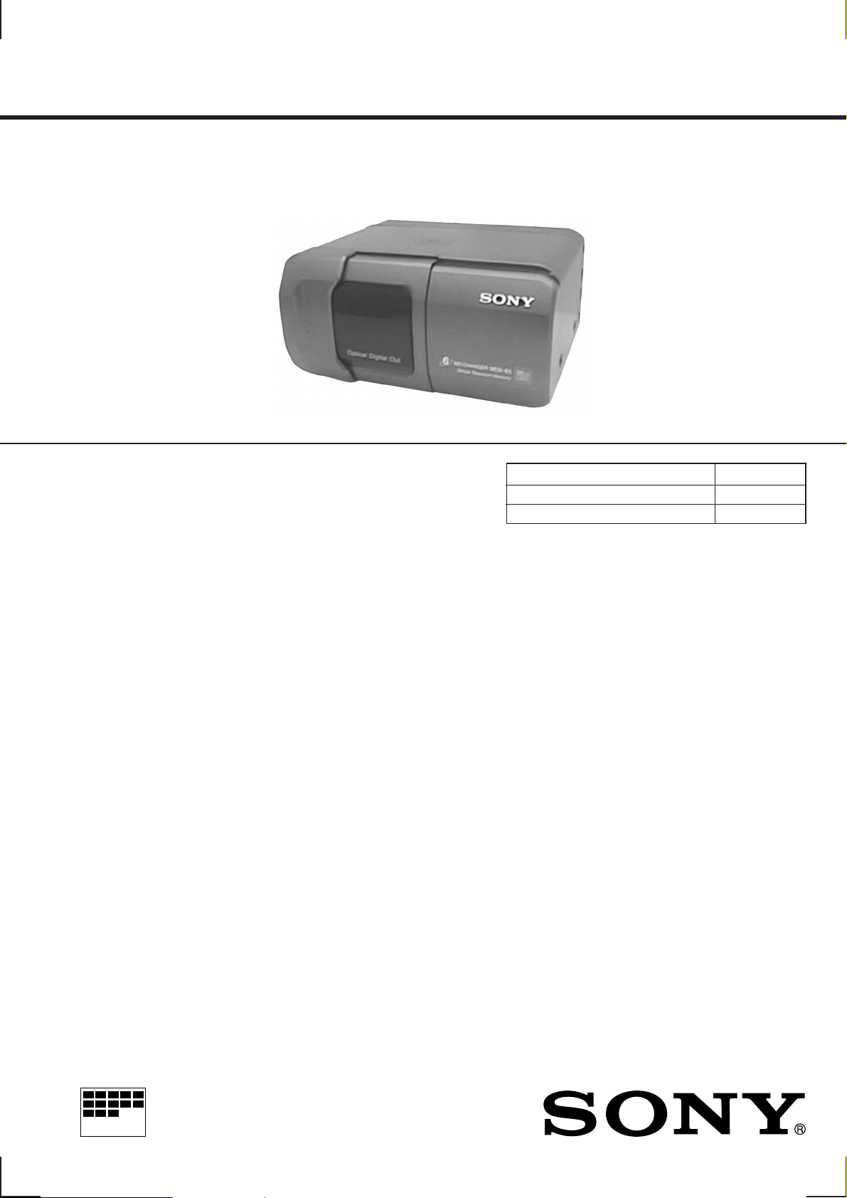
MDX-65
SERVICE MANUAL
Dolby noise reduction extension manufactured under license
from Dolby Laboratories Licensing Corporation.
“DOLBY” and the double-D symbol a are trademarks of Dolby
Laboratories Licensing Corporation.
SPECIFICATIONS
US Model
Canadian Model
AEP Model
UK Model
E Model
Model Name Using Similar Mechanism MDX-62
Mini Disc Mechanism Type MG-798K-133
Optical Pick-up Name KMS-241A/J2N
FEATURES
System Mini disc digital audio system
Laser Diode Properties
Material: GaAlAs
Wavelength: 780 nm
Emission Duration: Continuous
Laser output Power: Less than
44.6 µW*
* This output is the value measured at a distance of
200 mm from the objective lens surface on the
Optical Pick-up Block.
Frequency response
10 – 20,000 Hz
Wow and flutter Below measurable limit
Signal-to-noise ratio
95 dB
Outputs Bus control output (8 PIN)
Analog audio output (RCA PIN)
Current drain 300 mA (MD playback)
600 mA (during loading or ejecting a
disc)
Dimensions Approx. 176 × 83.5 × 142 mm
(7 × 3 3/8 × 5 18/32 in.) (w/h/d) not incl.
projecting parts and controls
Mass Approx. 1.1 kg (2 lb. 7 oz.)
Power requirement
12 V DC car battery (negative
ground)
Supplied accessories
Mounting hardware (1 set)
Bus cable 5.5 m (1)
RCA pin cord 5.5 m (1)
• U.S. and foreign patents licensed from Dolby
Laboratories Licensing Corporation.
• Design and specifications subject to change without
notice.
• Sony BUS system compatible with mobile MD
changers.
• Direct-in system for inserting and removing
MDs easily.
• No waiting time to change discs in continuous
play.
• The MD changer compartment has a built in light
for easy use even in the dark.
• 1 bit Digital/Analog converter for high quality
sound reproduction.
MICROFILM
MINIDISC CHANGER
– 1 –
Page 2

SECTION 4
DIAGRAMS
4-1. IC PIN DESCRIPTIONS
• IC100 CXA2523AR (RF AMP)
Pin No. Pin Name I/O Pin Description
1 I I I-V converted RF signal input (I) from detector of optical pick-up.
2 J I I-V converted RF signal input (J) from detector of optical pick-up.
3 VC O Center voltage (+1.65 V) generation output
4 – 9 A – F I Signal input (A to F) from detector of optical pick-up.
10 PD I Quantity monitor input of light from laser diode of optical pick-up.
11 APC O Laser amplifier output to automatic power control circuit.
12 APCREF I Reference voltage input for laser power setting.
13 GND — GND
14 TEMPI I Temperature sensor connecting pin (Not used in this set.)
15 TEMPR O Reference voltage output for temperature sensor. (Not used in this set.)
16 SWDT I Write data signal input from System controller (IC600).
17 SCLK I Serial clock signal input from System controller (IC600).
18 XLAT I Serial latch signal input from System controller (IC600).
19 XSTBY I Standby signal input (“L” : Standby) (Fixed at “H” in this set.)
20 FOCNT I Center frequency control voltage input of internal circuit filter (BPF22, BPF3T and EQ).
21 VREF O Reference voltage output (Not used in this set.)
22 EQADJ I Center frequency setting input of internal circuit filter (EQ).
23 3TADJ I Center frequency setting input of internal circuit filter (BPF3T).
24 VCC — Power supply pin (+3.3 V)
25 WBLADJ I Center frequency setting input of internal circuit filter (BPF22).
26 TE O Tracking error signal output to CXD2652AR (IC200).
27 CSLED I Connecting pin for low pass filter condenser of sled error signal.
28 SE O Sled error signal output to CXD2652AR (IC200).
29 ADFM O FM signal output of ADIP.
30 ADIN I FM signal input of ADIP by AC combination.
31 ADAGC I External condenser connecting pin for AGC of ADIP.
32 ADFG O ADIP double FM signal output (22.05 kHz ± 1 kHz) to CXD2652AR (IC200).
33 AUX O Support signal (I3 signal/temperature signal) output (Not used in this set.)
34 FE O Focus error signal output to CXD2652AR (IC200).
35 ABCD O Quantity signal output of light to CXD2652AR (IC200).
36 BOTM O Bottom hold signal output of quantity signal (RF/ABCD) of light to CXD2652AR (IC200).
37 PEAK O Peak hold signal output of quantity signal (RF/ABCD) of light to CXD2652AR (IC200).
38 RF O Playback EFM RF signal output to CXD2652AR (IC200).
39 RFAGC I External condenser connecting pin of AGC circuit for RF.
40 AGCI I RF signal input by AC combination.
41 COMPO O User comparator output pin (Not used in this set.)
42 COMPP I User comparator input pin (Fixed at “L” in this set.)
43 ADDC I External condenser connecting pin for low frequency interception of ADIP amplifier.
44 OPO O External condenser connect pin for lower cut of ADIP amplifier.
45 OPN I User operational amplifier inversion input pin (Fixed at “L” in this set.)
46 RFO O RF signal output
47 MORFI I RF signal input of MO by AC combination.
48 MORFO O RF signal output of MO.
– 11 –
Page 3

• IC600 µPD784216GC-027-8EU (SYSTEM CONTROLLER)
Pin No. Pin Name I/O Pin Description
1 M1 O Elevator motor (M904) drive signal output
2 M1 O Elevator motor (M904) drive signal output
3 M2 O Loading motor (M903) drive signal output
4 M2 O Loading motor (M903) drive signal output
5 MDMON O Mechanism deck system power control output (“H” : Power ON)
6 LES I Loading end sensor detection switch (S902) input
7 SES I Store end sensor detection switch (S903) input
8 HOME I Home position detection switch (S901) input (“L” : Home position)
9 VDD — Power supply pin (+5 V)
10 X2 — Main system clock connecting pin (14 MHz)
11 X1 — Main system clock connecting pin (14 MHz)
12 VSS — GND
13 XT2 — Sub system clock connecting pin (32.768 kHz)
14 XT1 — Sub system clock connecting pin (32.768 kHz)
15 RESET — System reset input
16 BU IN I Backup OFF detection input (“L” : Backup OFF)
17 BUS ON I BUS OFF detection of SONY BUS. (“H” : BUS OFF)
18 SQ SY I Sub code Q sync input from CXD2652AR (IC200).
19 STR SW I STOP switch (S600) input
20 — O Not used.
21 CC XINT I Interruption status input from CXD2652AR (IC200).
22 — O Not used.
23 AVDD — Power supply for A/D converter. (+5 V)
24 AVREF0 — Reference voltage for A/D converter.
25 INIT I Initial input pin at reset.
26 TEMP I Thermistor connecting pin for temperature detection.
27 EHS I Elevator height position detection input
28, 29 — I Connect to GND.
30 – 32 — O Connect to GND.
33 AVSS — Analog GND
34 ERR PWM O Error data output (Not used in this set.)
35 — O Not used.
36 AVREF1 — Reference voltage for D/A converter.
37, 38 — O Not used.
39 — — Not used.
40 MD SI I Read data signal input from CXD2652AR (IC200).
41 MD SO O Write data signal output to CXA2523AR (IC100) and CXD2652AR (IC200).
42 MD CKO O Serial clock signal output to CXA2523AR (IC100) and CXD2652AR (IC200).
43 — O Not used.
44 — — Not used.
45 UNISI I Serial data input for SONY BUS.
46 UNISO O Serial data output for SONY BUS.
47 UNI CKI I Serial clock input for SONY BUS.
48 LINKOFF O Link control signal output for SONY BUS. (“H” : Link OFF)
49 — O Not used.
50 — I Not used.
51, 52 D-BASS1, 2 O Digital D-BASS select output 1, 2 (Not used in this set.)
53 – 55 — O Not used.
56 – 59 MNT0 – 3 O Monitor 0 – 3 signal input from CXD2652AR (IC200).
60 AGING O Not used.
61 AGCHK O Not used.
62 TFTON O Not used.
– 12 –
Page 4

Pin No. Pin Name I/O Pin Description
63 — O Not used.
64 EE CS O Chip select output to EEPROM. (Not used in this set.)
65 EE CKO O Serial clock output to EEPROM. (Not used in this set.)
66 EE SIO I/O Data input from/output to EEPROM. (Not used in this set.)
67 SENS I Internal status input from CXD2652AR (IC200).
68 LIMIT SW I Optical pick-up innermost track limit position detection switch (S400) input
69 DOORSW I Front door open detection switch (S620) input (“L” : Open complete)
70 MD LAT O Serial latch signal output to CXA2523AR (IC100) and CXD2652AR (IC200).
71 MD RST O Reset signal output to CXD2652AR (IC200).
72 VSS — GND
73 MD ON O Servo system power control output (“H” : Power ON)
74 EMPH O O De-emphasis circuit control output (“H” : De-emphasis ON)
75 A ATT I Analog mute control input (“H” : Mute ON)
76 ILLON O Illumination lamp (PL620) light-up control output (“H” : Lamp light-up)
77 TSTSMD I Single mode setting pin (“L” : Single mode)
78 TSTCKO O Serial clock output to LED for TEST mode display. (Not used in this set.)
79 TSTSO O Serial data output to LED for TEST mode display. (Not used in this set.)
80 TSTMOD I TEST mode setting pin (“L” : TEST mode)
81 VDD — Power supply pin (+5 V)
82 – 85 TSTOUT0 – 3 O TEST key output pin of 4 × 8 matrix. (Not used in this set.)
86 – 93 TSTIN0 – 7 I TEST key input pin of 4 × 8 matrix. (Not used in this set.)
94 TEST/VPP — Fixed at “L” in this set.
95 DCS1 I Disc with/without detection 1 switch (S611) input (“H” : with disc)
96 DCS2 I Disc with/without detection 2 switch (S612) input (“H” : with disc)
97 DCS3 I Disc with/without detection 3 switch (S613) input (“H” : with disc)
98 DCS4 I Disc with/without detection 4 switch (S614) input (“H” : with disc)
99 DCS5 I Disc with/without detection 5 switch (S615) input (“H” : with disc)
100 DCS6 I Disc with/without detection 6 switch (S616) input (“H” : with disc)
– 13 –
Page 5

MDX-65
4-5. SCHEMATIC DIAGRAM — SERVO SECTION — • Refer to page 33 for Waveforms and page 35 for IC Block Diagrams.
– 21 – – 22 –
(Page 23)
Page 6

4-6. SCHEMATIC DIAGRAM — MAIN SECTION — • Refer to page 34 for Waveforms and page 37 for IC Block Diagrams.
MDX-65
(Page 22)
(Page 32)
– 23 – – 24 –
Page 7

4-9. SCHEMATIC DIAGRAM — POWER SECTION — • Refer to page 37 for IC Block Diagrams.
MDX-65
(Page 24)
– 31 – – 32 –
Page 8

µ
µ
• Waveforms
– Servo Section –
1 IC100 4 (A) PLAY MODE
200 mV/DIV, 10 µsec/DIV
2 IC100 8 (E) PLAY MODE
100 mV/DIV, 10 µsec/DIV
Approx.
150 mVp-p
Approx.
150 mVp-p
5 IC100 #• (RF) PLAY MODE
500 mV/DIV, 1 µsec/DIV
Approx.
1.1 Vp-p
6 IC100 #¢, IC200 ^∞ (FE) PLAY MODE
200 mV/DIV, 0.5 msec/DIV
400 mVp-p
9 IC200 @§ (XBCK)
354 ns
!º IC200 !§ (OSCI)
3.2 Vp-p
2.8 Vp-p
– Main Section –
1 IC600 !º (X2)
2 IC600 !¢ (XT1)
71 ns
2.7 Vp-p
2.6 Vp-p
5 IC500 1 (XT1)
3.2 Vp-p
89 ns
3 IC100 9 (F) PLAY MODE
100 mV/DIV, 10 µsec/DIV
4 IC100 1, 2 (I, J) PLAY MODE
100 mV/DIV, 10 µsec/DIV
Approx.
150 mVp-p
150 mVp-p
7 IC100 @§, IC200 &¢ (TE) PLAY MODE
500 mV/DIV, 0.5 msec/DIV
2.0 Vp-p
8 IC200 @∞ (LRCK)
3.2 Vp-p
44.3 ns
30.4 µs
3 IC500 4 (LRCK)
22.7
4 IC500 6 (BCK)
2.8 Vp-p
s
2.8 Vp-p
22.7
s
354 ns
– 33 – – 34 –
Page 9

• IC Block Diagrams
– Servo Section –
IC100 CXA2523AR
MORFO47MORFI46RFO45OPN
48
–
+
RFA1
+
–
AA
BB
CC
DD
EE
FF
–
–
–
–
–
–
–
GRVA
1
2
1
2
EBAL
FBAL
RFA2
OFST
+
–
+
–
HLPT
GRV
1I
2J
CVB
3VC
4A
IVR
5B
IVR
6C
IVR
7D
IVR
8E
IVR
9F
IVR
GSW
+
–
+
–
+
–
+
–
+
–
+
–
+
–
IV
OPO43ADDC42COMPP41COMPO40AGCI39RF AGC38RF37PEAK
44
USROP
EE'
–1
–2
–2
–1
–
–
–
–
+
+
–
–
–
–
+
+
ESW
FF'
+
–
–
+
–
+
BPF3T
BPF22
WBL
WBL
RFA3
PTGR
PBSW
ABCDA
FEA
ATA
EFB TESW
RF AGC EQ
USRC
PEAK
BOTTOM
WBL
ADIP
PTGR
PEAK3T
P-P
AGC
WBL
3T
EQ
3T
3T WBL
PBH
DET
–1
–2
–1
–2
DET
TEMP
EQ
AUX
SW
BPFC
SEA
TEA
VI CONV
TG
TG
36
BOTM
35
ABCD
34
FE
33
AUX
32 ADFG
31 ADAGC
30 ADIN
29 ADFM
28 SE
27 CSLED
26 TE
25 WBLADJ
15
AUXSW
TEMPR
COMMAND
SCRI - PARA
DECODE
17
16
SWDT
SCLK
BGR
VREF
24
23
22
21
20
19
18
XLAT
XSTBY
F0CNT
VREF
EQADJ
3TADJ
VCC
10PD
11APC
12APCREF
+
–
+
–
14
13
GND
TEMPI
– 35 –
Page 10

IC200 CXD2652AR
EFMO
100
1
MNT0
2
MNT1
MNT2
MNT3
SWDT
SCLK
XLAT
SRDT
SENS
XRST
SQSY
DQSY
RECP
XINT
TX
OSCI
OSCO
XTSL
NC
DVSS
DIN
DOUT
10
11
12
13
14
15
16
17
18
19
20
21
22
3
4
5
6
7
8
9
MONITOR
CONTROL
CPU I/F
SUBCODE
PROCESSOR
CLOCK
GENERATOR
DVSS
TEST3
TEST2
TEST1
FGIN
EACH
BLOCK
EACH
BLOCK
SPINDLE
SERVO
DECODER
EACH
BLOCK
SPFD
ADIP
99 98 97 96 95 94 93
SPRD
DIGITAL
AUDIO
I/F
SFDR91SRDR90FS489FRDR88FFDR87DVDD86TFDR85TRDR84LDDR83APCREF82DTRF81CKRF80XLRF79F0CNT78ADFG77APC76DCHG
92
PWM
GENERATOR
SERVO
DSP
SHOCK RESISTANT
MEMORY CONTROLLER
SAMPLING
RATE
CONVERTER
CONVERTER
A/D
AUTO
SEQUENCER
EFM/ACIRC
ENCODER/
ANALOG
MUX
DECODER
COMP
PLL
75
AUX2
74
TE
73
SE
72
AVSS
71
ADRB
70
ADRT
69
AVDD
68
ADIO
67
VC
66
AUX1
65
FE
64
ABCD
63
BOTM
62
PEAK
61
CLTV
60
FILO
59
FILI
58
PCO
57
PDO
56
AVSS
55
RFI
54
BIAS
53
AVDD
52
ASYI
51
ASYO
23
ADDT
24
DADT
25
LRCK
28
26
27
XBCK
DVDD
FS256
IC300 MPC17A38ZVMEL
VG
GNDPSOE
36 35 34 33 32 31 30 29 28 27 26 25 24 23 22 21 20 19
DC/DC
CONVERTER
VC
CLOCK
CLK
DETECTOR
ATRAC
ENCODER/DECODER
ADDRESS/DATA BUS A00 - A11, D0 - D3
42
41
40
39
A1138A0837A0736A0635A0534A0433A1032A0031A0130A0229A03
XOE
XCAS
DVSS
FO3
VD
FI3
RI3
DRIVER
PRE-DRIVER
VC VC
CONTROL
DRIVER
PRE-DRIVER
VC
CONTROL
VCVC
43
A09
PGND
VC
44
XWE
XRAS
PGND
DRIVER
PRE-DRIVER
CONTROL
RO3VDRO4
50
49D348D247D046D145
MVCI
PI4
VC
VC
PGND
FO4VDF/R4
DRIVER
PRE-DRIVER
CONTROL
VC
2 345 6 7 8 9 10 14
1
VC
LG
CLK
GND
RI1
VD
FI1
FO1
PGND
PGND
RO1
VD
RO2
– 36 –
PGND
15131211
181716
VD
FI2
RI2
FO2
Page 11

REFERENCE
VOLTAGE
S.C.P.
COMPARATOR 1
SWITCH
'ON'
AT
'H'
PWM
COMPARATOR
S.C.P.
COMPARATOR 2
DEAD-TIME
COMPARATOR
S.C.P.
LATCH
OSC
U.V.L.O
ERROR
AMP
–
+
+
–
+
–
+
–
–
+
5
6 7
8
1234
OUT
VCC
FEED BACK
INPUTSCP
DEAD-TIME
CONTROL
RT
GND
– Main Section –
IC500 PCM1718E-T1
1
XTI
2
DGND
VDD
3
4
LRCIN
DIN
5
6
BCKIN
7
ZERO
8
D/C R
9
VOUTR
10
AGND
– Power Section –
IC900 BA8272F-E2
INPUT
INTERFACE
DIGITAL
FILTER
NOISE SHAPER
5 LEVEL
DAC
LOWPASS
FILTER
CMOS
AMP
CLK
CONTROL
MODE
CONTROL
5 LEVEL
DAC
LOWPASS
FILTER
CMOS
AMP
20
19
18
17
16
15
14
13
12
11
XTO
CLKO
MUTE
DM1
DM0
RSTB
FORMAT
D/C L
VOUTL
VCC
IC700, 701 LB1638MTP-T1
1
GND
2
IN1
VCC
3
4
IN2
5 6
GND
CONTROL LOGIC
IC970 TL5001CPS-E20
10
N.C.
9
OUT1
VS
8
7
OUT2
N.C.
VCC
1
BUS ON OUT
BUS ON
2 3
BUS ON IN
LINK OFF
CLK OUT
5 6 7
4
GND
VREF
BUS CLK
DATA OUT
BUS DATA
DATA IN
RESET
891014 13 12 11
RESET
SWITCH
BUS RESET
– 37 –
 Loading...