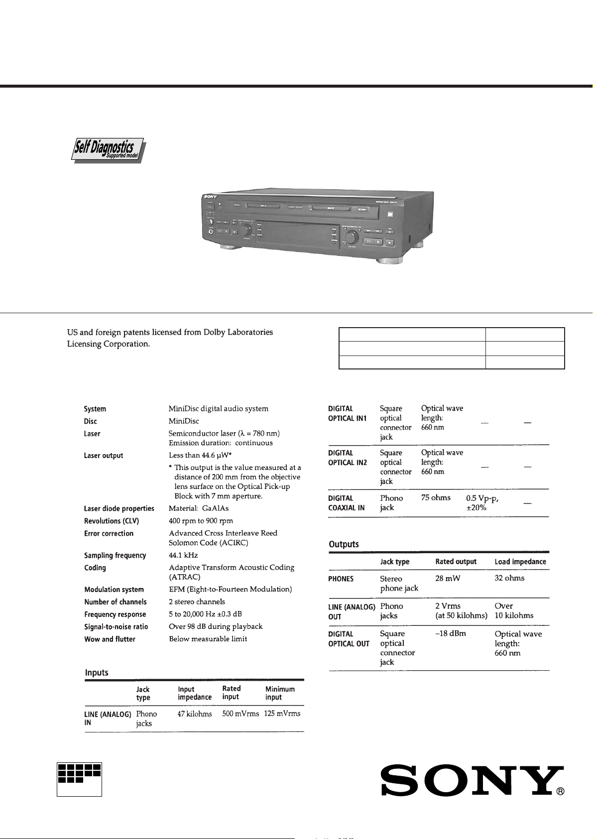
Sony MDSW-1 Service manual
MICROFILM
MDS-W1
SERVICE MANUAL
SPECIFICATIONS
AEP Model
Model Name Using Similar Mechanism MDS-JE520
MD Mechanism Type MDM-5B
Optical Pick-up Type KMS-260A/J1N
— Continued on next page —
MINIDISC DECK
– 1 –
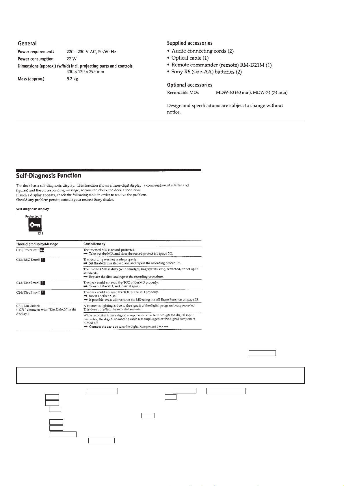
SELF-DIAGNOSIS FUNCTION
The self-diagnosis function consists of error codes for customers which are displayed automatically when errors occur, and error codes which
show the error history in the test mode during servicing. For details on how to view error codes for the customer, refer to the following box
in the instruction manual. For details on how to check error codes during servicing, refer to the following “Procedure for using the SelfDiagnosis Function (Error History Display Mode)”.
Procedure for using the Self-Diagnosis Function (Error History Display Mode).
Note: Perform the self-diagnosis function in the “error history display mode” in the test mode. The following describes the least required
procedure. Be careful not to enter other modes by mistake. If you set other modes accidentally, press the MENU/NO button to exit
the mode.
As this unit uses two mechanism Deck A and Deck B, it carries out self-diagnosis for eac h deck. For buttons or knobs not specified as
(Deck A) or (Deck B) in the procedure, use that of the corresponding deck.
1. With the power ON, press the 0 (Deck B) button while pressing the OUTPUT and CLEAR (Deck A) buttons together.
2. Rotate the AMS knob and when “(Service)” is displayed, press the YES button.
3. Rotate the AMS knob and display “ERR DP MODE”.
4. Pressing the YES button sets the error history mode and displays “total rec”.
5. Select the contents to be displayed or executed using the AMS knob.
6. Pressing the AMS knob will display or execute the contents selected.
7. Pressing the AMS knob another time returns to step 4.
8. Pressing the MENU/NO button displays “ERROR DP MODE” and exits the error history mode.
9. To exit the test mode, press the MD SYNC button. The unit sets into the STANDBY state, and the test mode ends.
– 2 –
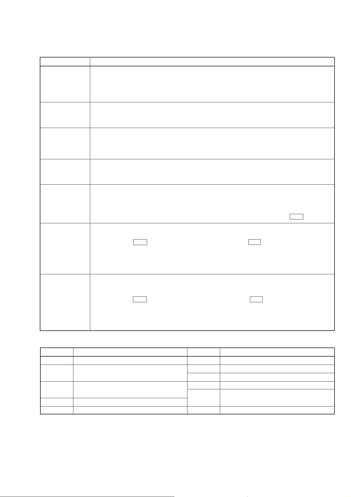
ITEMS OF ERROR HISTORY MODE ITEMS AND CONTENTS
Selecting the Test Mode
Display
total rec
total play
retry err
total err
err history
er refresh
Details of History
Displays the recording time.
Displayed as “rππππππh”.
The displayed time is the total time the laser is set to the high power state.
This is about 1/4 of the actual recording time.
The time is displayed in decimal digits from 0h to 65535h.
Displays the play time.
Displayed as “pππππππh”. The time displayed is the total actual play time. Pauses are not counted.
The time is displayed in decimal digits from 0h to 65535h.
Displays the total number of retries during recording and number of retry errors during play.
Displayed as “rππ pππ”.
“r” indicates the retries during recording while “p” indicates the retry errors during play.
The number of retries and retry errors are displayed in hexadecimal digits from 00 to FF.
Displays the total number of errors.
Displayed as “total ππ”.
The number of errors is displayed in hexadecimal digits from 00 to FF.
Displays the 10 latest errors.
Displayed as “0π E@@”.
π indicates the history number. The smaller the number, the more recent is the error. (00 is the latest).
@@ indicates the error code.
Refer to the following table for the details. The error history can be switched by rotating the AMS knob.
Mode which erases the “retry err”, “total err”, and “err history” histories.
When returning the unit to the customer after completing repairs, perform this to erase the past error history,
After pressing the AMS button and “er refresh?” is displayed, press the YES button to erase the history.
“Complete!” will be displayed momentarily.
Be sure to check the following when this mode has been executed.
• The data has been erased.
• The mechanism operates normally when recording and play are performed.
tm refresh
Table of Error Codes
Error Code
E00
E01
E02
E03
E04
No error
Disc error. PTOC cannot be read
(DISC ejected)
Disc error. UTOC error
(DISC not ejected)
Loading error
Address cannot be read (Servo has deviated)
Mode which erases the “total rec” and “total play” histories.
These histories serve as approximate indications of when to replace the optical pickup.
If the optical pickup has been replaced, perform this operation and erase the history.
After pressing the AMS button and “tm refresh?” is displayed, press the YES button to erase the history.
“Complete!” will be displayed momentarily.
Be sure to check the following when this mode has been executed.
• The data has been erased.
• The mechanism operates normally when recording and play are performed.
Details of Error
Error Code
E05
E06
E07
E08
E09
E0A
Details of Error
FOK has deviated
Cannot focus (Servo has deviated)
Recording retry
Recording retry error
Playback retry error
(Access error)
Play retry error (C2 error)
– 3 –
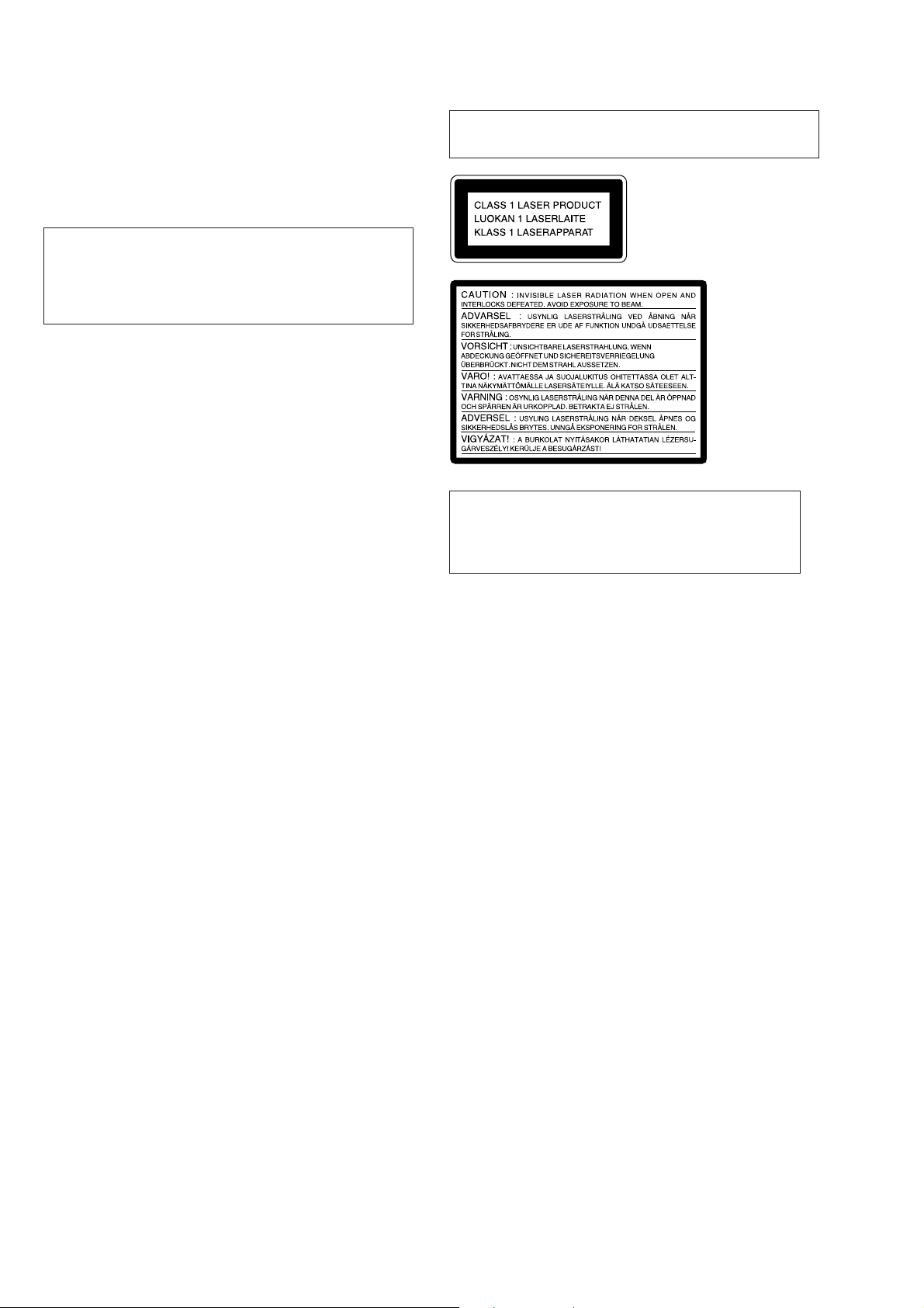
CAUTION
Danger of explosion if battery is incorrectly replaced.
Replace only with the same or equivalent type recommended by
the equipment manufacturer.
Discard used batteries according to manufacture’s instructions.
ADVARSEL!
Laser component in this product is capable of emitting radiation
exceeding the limit for Class 1.
This appliance is classified as
a CLASS 1 LASER product.
The CLASS 1 LASER PRODUCT MARKING is located on
the rear exterior.
Lithiumbatteri - Eksplosionsfare ved fejlagtig håndtering.
Udskiftning må kun ske med batteri af samme fabrikat og type.
Levér det brugte batteri tilbage til leverandøren.
ADVARSEL
Eksplosjonsfare ved feilakting skifte av batteri.
Benytt samme batteritype eller en tilsvarende type anbefalt av
apparatfabrikanten.
Brukte batterier katterier kasseres i henhold til fabrikantens
VARNIG
Explosionsfara vid felaktigt batteribyte.
Använd samma batterityp eller en likvärdig typ som rekommender as
av apparattillverkaren.
Kassera använt batteri enligt gällande föreakrifter.
VAROITUS
Parist voi räjähtää, jos se on virheellisesti asennettu.
V aihda paristo ainoastaan laitev almistajan suosittelemaan tyyppiin.
Hävitä käytetty paristo valmistajan ohjeiden mukaisesti.
The following
caution label is
located inside of
the unit.
CAUTION
Use of controls or adjustments or performance of procedures
other than those specified herein may result in hazardous radiation exposure.
Notes on chip component replacement
• Never reuse a disconnected chip component.
• Notice that the minus side of a tantalum capacitor may be
damaged by heat.
Flexible Circuit Board Repairing
• Keep the temperature of soldering iron around 270˚C
during repairing.
• Do not touch the soldering iron on the same conductor of the
circuit board (within 3 times).
• Be careful not to apply force on the conductor when soldering
or unsoldering.
SAFETY-RELATED COMPONENT WARNING !!
COMPONENTS IDENTIFIED BY MARK ! OR DO TTED LINE
WITH MARK ! ON THE SCHEMATIC DIAGRAMS AND IN
THE PARTS LIST ARE CRITICAL TO SAFE OPERATION.
REPLACE THESE COMPONENTS WITH SONY PARTS
WHOSE PART NUMBERS APPEAR AS SHOWN IN THIS
MANUAL OR IN SUPPLEMENTS PUBLISHED BY SONY.
– 4 –

TABLE OF CONTENTS
1. SERVICING NOTE .......................................................... 6
2. GENERAL ........................................................................ 11
3. DISASSEMBLY
3-1. Front Panel ......................................................................... 35
3-2. Slider (Cam) ........................................................................ 35
3-3. Base Unit (MBU-5B) and BD Board .................................. 36
3-4. SW Board and Loading Motor (M103) ..............................36
4. TEST MODE ..................................................................... 37
5. ELECTRICAL ADJUSTMENTS ............................... 41
6. DIAGRAMS
6-1. Circuit Boards Location ...................................................... 50
6-2. Block Diagrams
• BD Section .......................................................................51
• Input/Output Section ........................................................53
• Control Section ................................................................ 55
• Power Section .................................................................. 58
6-3. Printed Wiring Board – BD Section –................................. 61
6-4. Schematic Diagram – BD (1/2) Section – ...........................63
6-5. Schematic Diagram – BD (2/2) Section – ...........................65
6-6. Schematic Diagram – Jack (1/2) Section – ......................... 67
6-7. Schematic Diagram – Jack (2/2) Section – ......................... 69
6-8. Printed Wiring Board – Jack Section – ............................... 71
6-9. Printed Wiring Board – Main Section –..............................73
6-10. Schematic Diagram – Main (1/5) Section – ......................77
6-11. Schematic Diagram – Main (2/5) Section – ......................79
6-12. Schematic Diagram – Main (3/5) Section – ......................81
6-13. Schematic Diagram – Main (4/5) Section – ......................83
6-14. Schematic Diagram – Main (5/5) Section – ......................85
6-15. Schematic Diagram – BD Switch Section – ..................... 87
6-16. Printed Wiring Board – BD Switch Section –................... 87
6-17. Printed Wiring Board – Panel Section –............................ 89
6-18. Schematic Diagram – Panel Section – .............................. 91
6-19. Printed Wiring Board – Power Section – .......................... 93
6-20. Schematic Diagram – Power Section – .............................95
6-21. Printed Wiring Board – Trans Section – ........................... 97
6-22. Schematic Diagram – Trans Section – .............................. 99
6-23. IC Block Diagrams .........................................................101
6-24. IC Pin Functions .............................................................105
7. EXPLODED VIEWS
7-1. Case Section ...................................................................... 115
7-2. Front Panel Section ........................................................... 116
7-3. Chassis Section ................................................................. 117
7-4. Mechanism Deck Section (MDM-5B) .............................. 118
7-5. Base Unit Section (MBU-5B) ........................................... 119
8. ELECTRICAL PARTS LIST ...................................... 120
– 5 –
SECTION 1
3
r
SERVICING NOTE
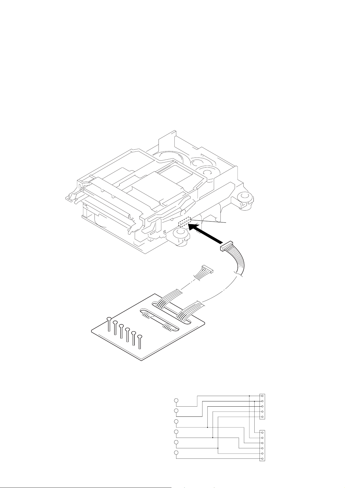
JIG FOR CHECKING BD BOARD WAVEFORM
The special jig (J-2501-149-A) is useful for checking the waveform of the BD board. The names of terminals and the checking items to be
performed are shown as follows.
GND : Ground
I+3V : For measuring IOP (Check the deterioration of the optical pick-up laser)
IOP : For measuring IOP (Check the deterioration of the optical pick-up laser)
TEO : TRK error signal (Traverse adjustment)
VC : Reference level for checking the signal
RF : RF signal (Check jitter)
Mechanism deck
RF
VC
TEO
IOP
I+3V
CN110
6P connecto
5P Connector
GND
1
RF
VC
TEO
IOP
I+3V
GND
RF
VC
For
TEO
MDM-
IOP
I-3V
5
1
VC
RF
For
TEO
MDM-5
IOP
I+3V
6
GND
– 6 –

IOP DATA RECORDING AND DISPLAY WHEN PICKUP AND NON-V OLA TILE MEMOR Y (IC171 OF BD BOARD)
ARE REPLACED
The IOP value labeled on the pick-up can be recorded in the non-volatile memory . By recording the value, it will eliminate the need to look
at the value on the label of the optical pick-up. When replacing the pick-up or non-volatile memory (IC171 of BD board), record the IOP
value on the pick-up according to the following procedure.
For buttons or knobs not specified as (Deck A) or (Deck B) in the procedure, use that of the corresponding deck.
Record Precedure:
1. With the power ON, press the 0 (Deck B) button while pressing the OUTPUT and CLEAR (Deck A) buttons together.
2. Rotate the AMS knob to display “(Service)”, and press the YES button.
3. Rotate the AMS knob to display “lop.Write” (S: 28), and press the YES button.
4. The display becomes “Ref=@@@.@” (@ is an arbitrary number) and the numbers which can be changed will blink.
5. Input the IOP value written on the optical pick-up.
To select the number : Rotate the AMS knob.
To select the digit :Press the AMS knob.
6. When the YES button is pressed, the display becomes “Measu=@@@.@” (@ is an arbitrary number).
7. As the adjustment results are recorded for the 6 value. Leave it as it is and press the YES button.
8. The value will be recorded in the non-volatile memory and the display will become “Iop Write”.
9. Press the MD SYNC button to complete.
Display Precedure:
1. With the power ON, press the 0 (Deck B) button while pressing the OUTPUT and CLEAR (Deck A) buttons together.
2. Rotate the AMS knob to display “(Service)”, and press the YES button.
3. Rotate the AMS knob to display “lop.Read” (S: 27).
4. “@@.@/##.#” is displayed and the recorded contents are displayed.
@@.@ : indicates the Iop value labeled on the pick-up.
##.# : indicates the Iop value after adjustment
5. To end, press the AMS button or MENU/NO button to display “Iop Read”. Then press the MD SYNC button.
– 7 –

CHECKS PRIOR TO PARTS REPLACEMENT AND ADJUSTMENTS
Before performing repairs, perform the following checks to determine the faulty locations up to a certain extent.
Details of the procedures are described in “5 Electrical Adjustments”.
Laser power check
(5-6-2 : See page 44)
Traverse check
(5-6-3 : See page 44)
Focus bias check
(5-6-4 : See page 45)
C PLAY check
(5-6-5 : See page 45)
Self-recording/playback
check
(REC/PLAY)
(5-6-6 : See page 45)
TEMP check
(Temperature
compensation
offset check)
(5-6-1 : See page 44)
Criteria for Determination
(Unsatisfactory if specified value is not satisfied)
• 0.9 mW power
Specified value : 0.84 to 0.92 mW
• 7.0 mW power
Specified value : 6.8 to 7.2 mW
lop (at 7mW)
• Labeled on the optical pickup
Iop value ± 10mA
• Traverse waveform
Specified value : Below 10% offset
• Error rate check
Specified value : For points a, b, and c
C1 error : Below 220
AD error : Below 2
• Error rate check
Specified value:
a.When using test disc (MDW-74/AU-1)
C1 error : Below 80
AD error : Below 2
b.When using check disc (TDYS-1)
C1 error : Below 50
• CPLAY error rate check
Specified value:
C1 error : Below 80
AD error : Below 2
• Unsatisfactory if displayed as T=@@ (##) (NG”
NG
(@@, ## are both arbitrary numbers)
Measure if unsatisfactory:
• Clean the optical pick-up
• Adjust again
• Replace the optical pick-up
• Replace the optical pick-up
• Replace the optical pick-up
• Replace the optical pick-up
• Replace the optical pick-up
If always unsatisfactory:
• Replace the overwrite head
• Check for disconnection of the circuits around the
overwrite head
If occasionally unsatisfactory:
• Check if the overwrite head is distorted
• Check the mechanism around the sled
• Check for disconnection of the circuits around D101
(BD board)
• Check the signals around IC101, IC121, CN102,
CN103 (BD board)
Note:
The criteria for determination above is intended merely to determine if satisfactory or not, and does not serve as the specifie d value for
adjustments.
When performing adjustments, use the specified values for adjustments.
FORCED RESET
The system microprocessor can be reset in the following procedure.
Use these procedure when the unit cannot be operated normally due to the overrunning of the microprocessor, etc.
Procedure :
Disconnect the power plug from the outlet, short-circuit Pins 1 and 2 of CN302 of the MAIN board and discharge the backup battery.
[MAIN BOARD] (Component Side)
3
21
CN302
Complete lighting of fluorescent display tube
The fluorescent display tube can be lit completely by the following method:
With the power ON, press the TIMER button while pressing the p (Deck A) and MENU/NO (Deck A) buttons.
To turn off, press the DISPLAY button.
– 8 –
RETRY CAUSE DISPLAY MODE
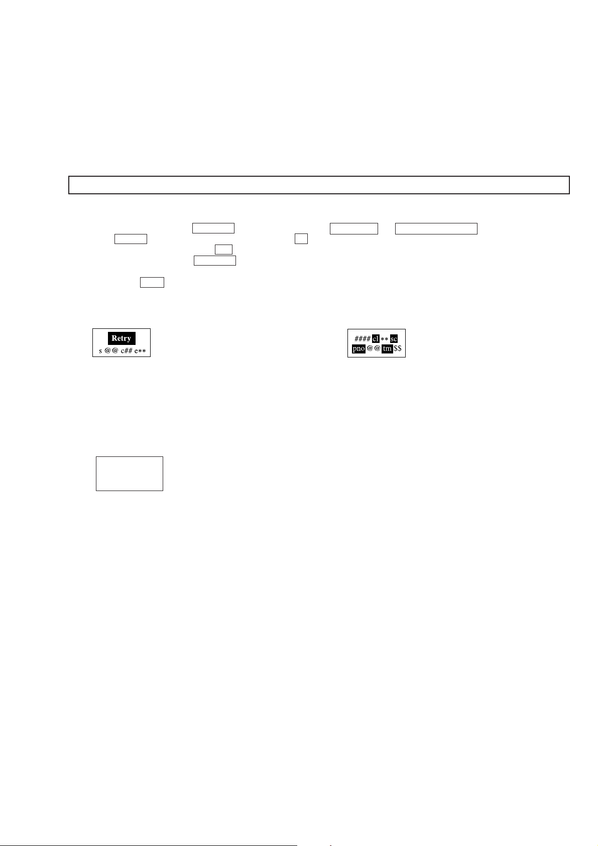
• In this test mode, the causes for retry of the unit during recording can be displayed on the fluorescent indicator tube. During playback, the
“track mode” for obtaining track information will be set.
This is useful for locating the faulty part of the unit.
• The following will be displayed :
During recording and stop : Retry cause, number of retries, and number of retry errors.
During playback : Information such as type of disc played, part played, copyright.
These are displayed in hexadecimal.
For buttons or knobs not specified as (Deck A) or (Deck B) in the procedure, use that of the corresponding deck.
Precedure:
1. Load recordable discs (the contents will be erased) in both decks.
2. With the STOP state, press the DISPLAY button while pressing the p (Deck A) and MENU/NO (Deck A) buttons together.
3. Press the r REC button to start recording. Then press the P button and start recording.
4. To check the “track mode”, press the · button to start play.
5. To exit the test mode, press the DISPLAY button on the STOP state.
If the test mode cannot be exited, refer to “Forced Reset” on page 8.
Note: Rotating the AMS knob during STOP will display as shown in Fig. 3. This is however not used in servicing.
Fig. 1 Reading the Test Mode Display
(During recording and stop)
Fluorescent display tube display
@@ : Cause of retry
## : Number of retries
** : Number of retry errors
Fig. 3. (This display is not used in servicing.)
@@/@@/@@
maker : @@
model : @@
Fluorescent display tube display
@@ : Any number
Fig. 2 Reading the Test Mode Display
(During playback)
Fluorescent display tube display
@@ : Parts No. (name of area named on TOC)
## : Cluster
** : Sector
$$ : Track mode (Track information such as copyright
information of each part)
} Address (Physical address on disc)
– 9 –
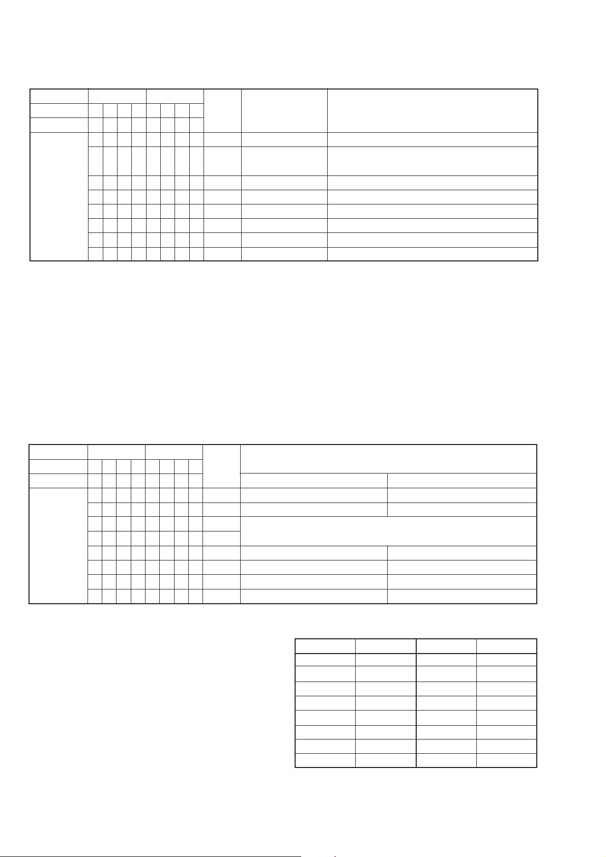
Reading the Retry Cause Display
Higher Bits
Hexadecimal
Bit
Binary
Reading the Display:
Convert the hexadecimal display into binary display. If more than two causes, they will be added.
Example
When 42 is displayed:
Higher bit : 4 = 0100 n b6
Lower bit : 2 = 0010 n b1
In this case, the retry cause is combined of “CLV unlock” and “ader5”.
When A2 is displayed:
Higher bit : A = 1010 n b7+b5
Lower bit : 2 = 0010 n b2
The retry cause in this case is combined of “access fault”, “IVR rec error”, and “ader5”.
84218421
b7 b6 b5 b4 b3 b2 b1 b0
00000001
00000010
00000100
00001000
00010000
00100000
01000000
10000000
Lower Bits
Hexa-
decimal
01
02
04
08
10
20
40
80
Cause of Retry Occurring conditions
shock
ader5
Discontinuous address
DIN unlock
FCS incorrect
IVR rec error
CLV unlock
Access fault
When track jump (shock) is detected
When ADER was counted more than five times
continuously
When ADIP address is not continuous
When DIN unlock is detected
When not in focus
When ABCD signal level exceeds the specified range
When CLV is unlocked
When access operation is not performed normally
Reading the Track Mode Display
Higher Bits Lower Bits
Hexadecimal
Bit
Binary
Reading the Display:
Convert the hexadecimal display into binary display. If more than
two causes, they will be added.
Example
When 84 is displayed:
Higher bit : 8 = 1000 n b7
Lower bit : 4 = 0100 n b2
In this case, as b2 and b7 are 1 and others are 0, it can be
determined that the retry cause is combined of “emphasis OFF”,
“monaural”, “original”, “copyright e xists”, and “write allowed”.
Example
When 07 is displayed:
Higher bit : 0 = 1000 n All 0
Lower bit : 7 = 0111 n b0+b1+b2
In this case, as b0, b1, and b2 are 1 and others are 0, it can be
determined that the retry cause is combined of “emphasis ON”,
“stereo”, “original”, “copyright exists”, and “write prohibited”.
84218421
b7 b6 b5 b4 b3 b2 b1 b0
00000001
00000010
00000100
00001000
00010000
00100000
01000000
10000000
Hexa-
decimal
01
02
04
08
10
20
40
80
Emphasis OFF
Monaural
This is 2-bit display. Normally 01.
01:Normal audio. Others:Invalid
Audio (Normal)
Original
Copyright
Write prohibited
– 10 –
Details
When 0 When 1
Emphasis ON
Stereo
Invalid
Digital copy
No copyright
Write allowed
Hexadecimal n Binary Conversion Table
Hexadecimal Binary Hexadecimal Binary
0
1
2
3
4
5
6
7
0000
0001
0010
0011
0100
0101
0110
0111
8
9
A
B
C
D
E
F
1000
1001
1010
1011
1100
1101
1110
1111
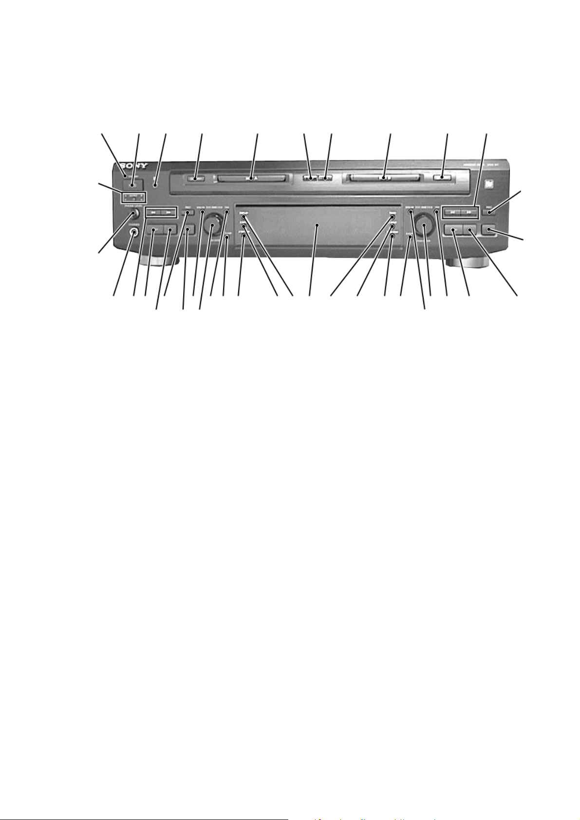
Front Panel
SECTION 2
GENERAL
2 4 6 7 8 9 10 11
35
1
37
323330343536
2931
Location of Parts and Controls
1920 14
1617242526 2122232728
15
18
12
13
1 OUTPUT button and A. B indicator
2 STANDBY indicator
3 1/u (Power) button
4 Remote sensor
5 § EJECT (Deck A) button
6 DISK compartment (Deck A)
7 RELAY button and indicator
8 MD SYNC button and indicator
9 DISK compartment (Deck B)
10 § EJECT (Deck B) button
11 0, ) (Deck B) button
12 r REC (Deck B) button
13 p (STOP) (Deck B) button
14 P (P AUSE) (Deck B) button
15 · (PLAY) (Deck B) button
16 YES (Deck B) button
17 ≠ AMS ± (PUSH ENTER) (Deck B) knob
18 MENU/NO (Deck B) button
19 CLEAR (Deck B) button
* AMS is the abbreviation for Automatic Music Sensor.
20 B TIME/CHAR button
21 B INPUT button
22 TIMER button
23 Display window
24 DISPLAY button
25 A INPUT button
26 A TIME/CHAR button
27 CLEAR (Deck A) button
28 YES (Deck A) button
29 ≠ AMS ± (PUSH ENTER) (Deck A) knob
30 MENU/NO (Deck A) button
31 p (STOP) (Deck A) button
32 r REC (Deck A) button
33 P (P AUSE) (Deck A) button
34 · (PLAY) (Deck A) button
35 0, ) (Deck A) button
36 PHONES jack
37 PHONE LEVEL knob
– 11 –
– 12 –
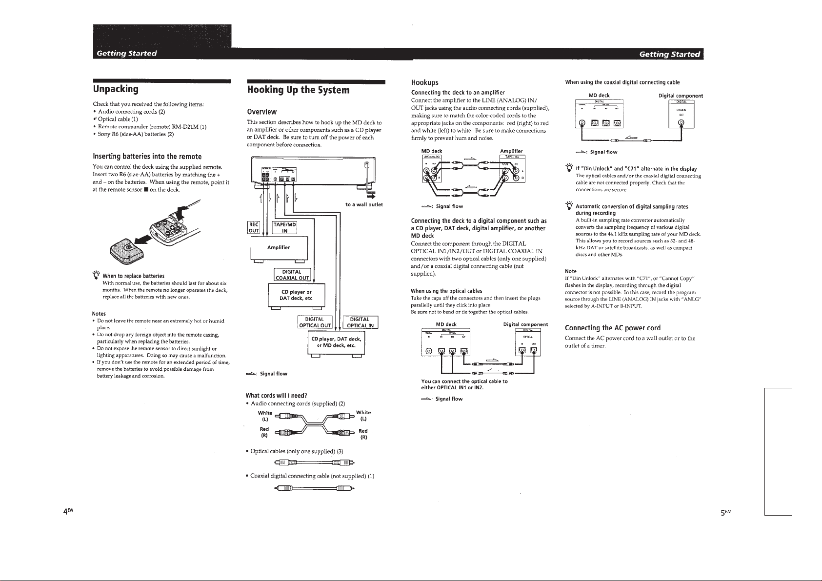
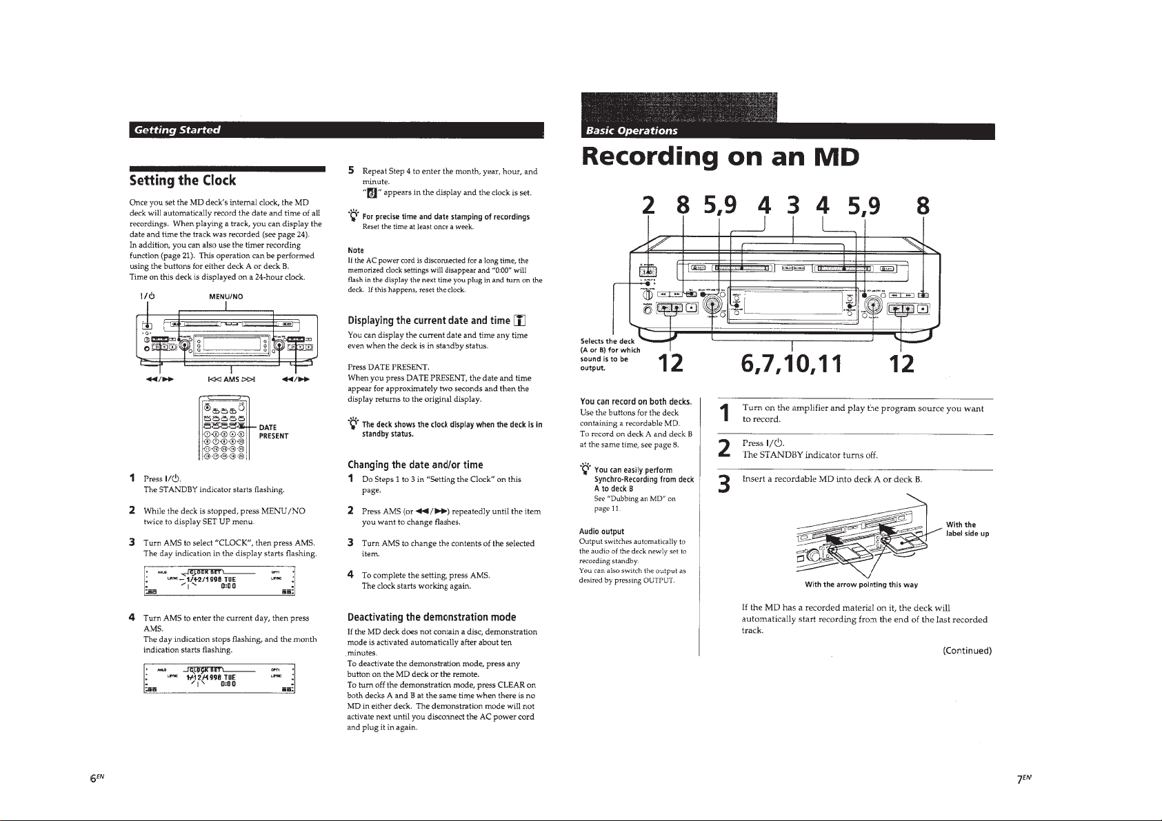
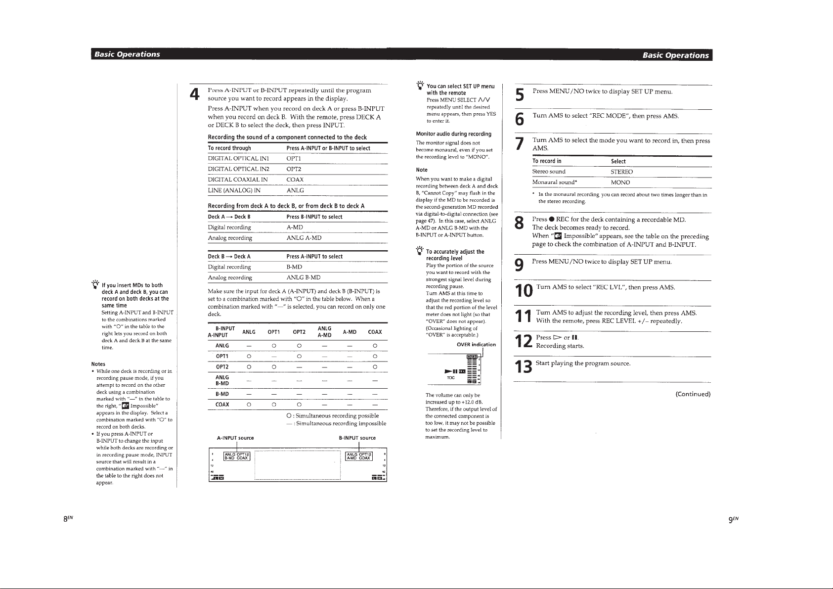
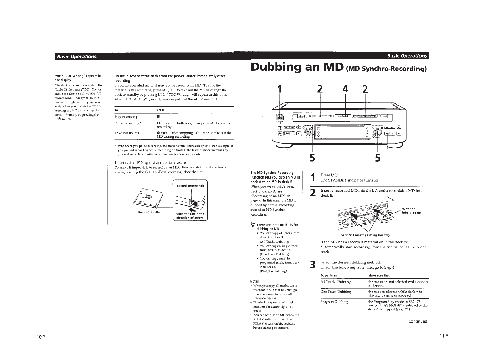
This section is extracted from
instruction manual.
– 13 –
– 14 –
– 15 –
– 16 –
– 17 –
– 18 –
– 19 –
– 20 –
– 21 –
– 22 –
– 24 –
– 25 –
– 26 –
– 27 –
– 28 –
– 29 –
– 30 –
 Loading...