

Sony MDSS-38 Service manual
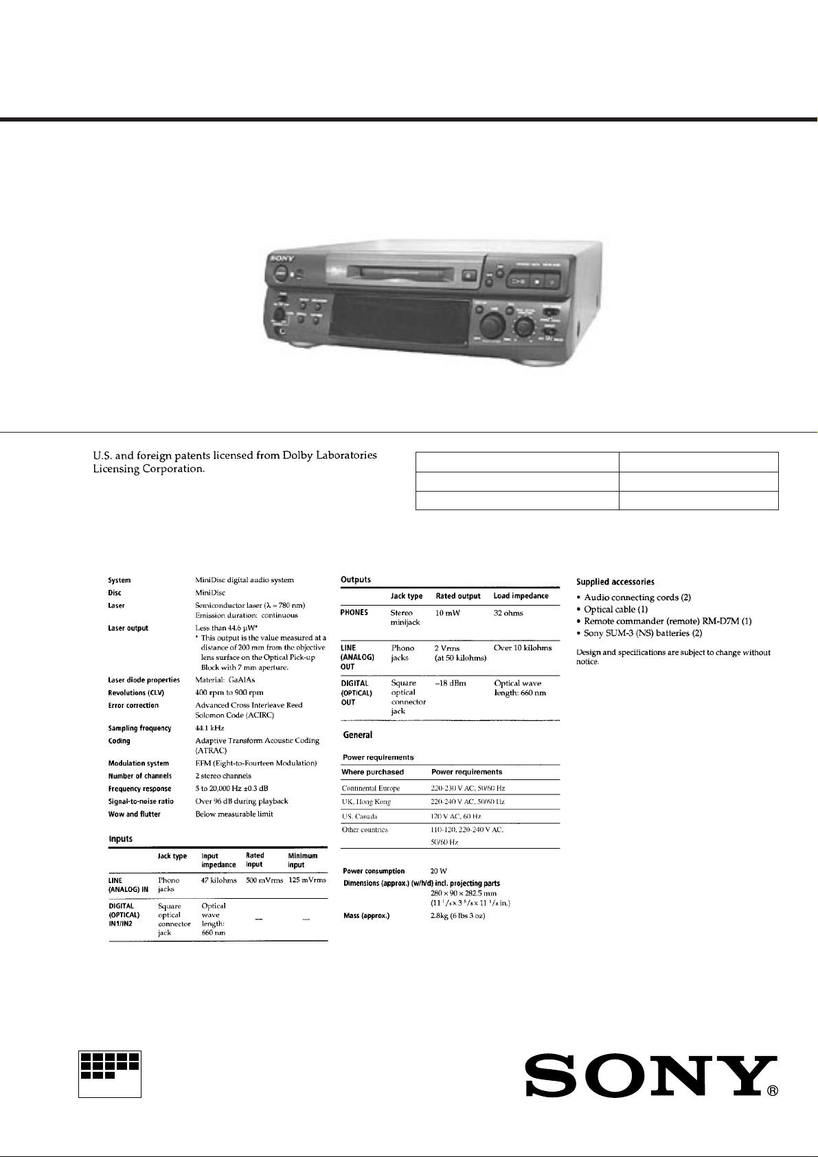
MDS-S38
SERVICE MANUAL
Photo: Black
Model Name Using Similar Mechanism MDS-S37
MD Mechanism Type MDM-3B
Optical Pick-up Type KMS-260A/J1N
SPECIFICATIONS
US Model
Canadian Model
AEP Model
UK Model
E Model
MICROFILM
MINIDISC DECK
— 1 —
CAUTION
Danger of explosion if battery is incorrectly replaced.
Replace only with the same or equivalent type recommended by
the equipment manufacturer.
Discard used batteries according to manufacture’s instructions.
ADVARSEL!
Lithiumbatteri - Eksplosionsfare ved fejlagtig håndtering.
Udskiftning må kun ske med batteri af samme fabrikat og type.
Levér det brugte batteri tilbage til leverandøren.
ADVARSEL
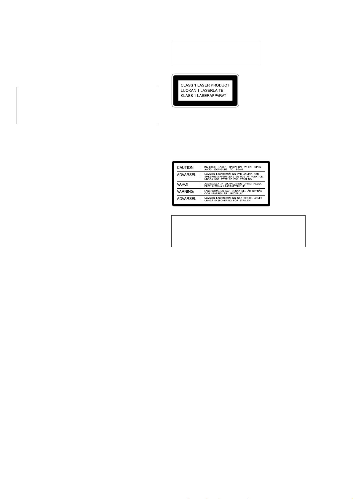
The laser component in this product is
capable of emitting radiation exceeding
the limit for Class 1.
This appliance is classified as a CLASS 1
LASER product. The CLASS 1 LASER
PRODUCT MARKING is located on the
rear exterior.
Eksplosjonsfare ved feilakting skifte av batteri.
Benytt samme batteritype eller en tilsvarende type anbefalt av
apparatfabrikanten.
Brukte batterier katterier kasseres i henhold til fabrikantens
VARNIG
Explosionsfara vid felaktigt batteribyte.
Använd samma batterityp eller en likvärdig typ som rekommenderas
av apparattillverkaren.
Kassera använt batteri enligt gällande föreakrifter.
VAROITUS
Parist voi räjähtää, jos se on virheellisesti asennettu.
V aihda paristo ainoastaan laite valmistajan suosittelemaan tyyppiin.
Hävitä käytetty paristo valmistajan ohjeiden mukaisesti.
The following caution label is located
inside the unit.
CAUTION
Use of controls or adjustments or performance of procedures
other than those specified herein may result in hazardous radiation exposure.
Notes on chip component replacement
• Never reuse a disconnected chip component.
• Notice that the minus side of a tantalum capacitor may be
damaged by heat.
Flexible Circuit Board Repairing
• Keep the temperature of soldering iron around 270˚C
during repairing.
• Do not touch the soldering iron on the same conductor of the
circuit board (within 3 times).
• Be careful not to apply force on the conductor when soldering
or unsoldering.
SAFETY-RELATED COMPONENT WARNING !!
COMPONENTS IDENTIFIED BY MARK ! OR DO TTED LINE
WITH MARK ! ON THE SCHEMATIC DIAGRAMS AND IN
THE PARTS LIST ARE CRITICAL TO SAFE OPERATION.
REPLACE THESE COMPONENTS WITH SONY PARTS
WHOSE PART NUMBERS APPEAR AS SHOWN IN THIS
MANUAL OR IN SUPPLEMENTS PUBLISHED BY SONY.
ATTENTION AU COMPOSANT AYANT RAPPORT
À LA SÉCURITÉ!!
LES COMPOSANTS IDENTIFIÉS P AR UNE MARQUE ! SUR
LES DIAGRAMMES SCHÉMATIQUES ET LA LISTE DES
PIÈCES SONT CRITIQUES POUR LA SÉCURITÉ DE
FONCTIONNEMENT . NE REMPLA CER CES COMPOSANTS
QUE PAR DES PIÈCES SONY DONT LES NUMÉROS
SONT DONNÉS DANS CE MANUEL OU DANS LES
SUPPLÉMENTS PUBLIÉS PAR SONY.
— 2 —
SAFETY CHECK-OUT
TABLE OF CONTENTS
After correcting the original service problem, perform the following safety checks before releasing the set to the customer:
Check the antenna terminals, metal trim, “metallized” knobs, screws,
and all other exposed metal parts for A C leakag e. Check leakage as
described below.
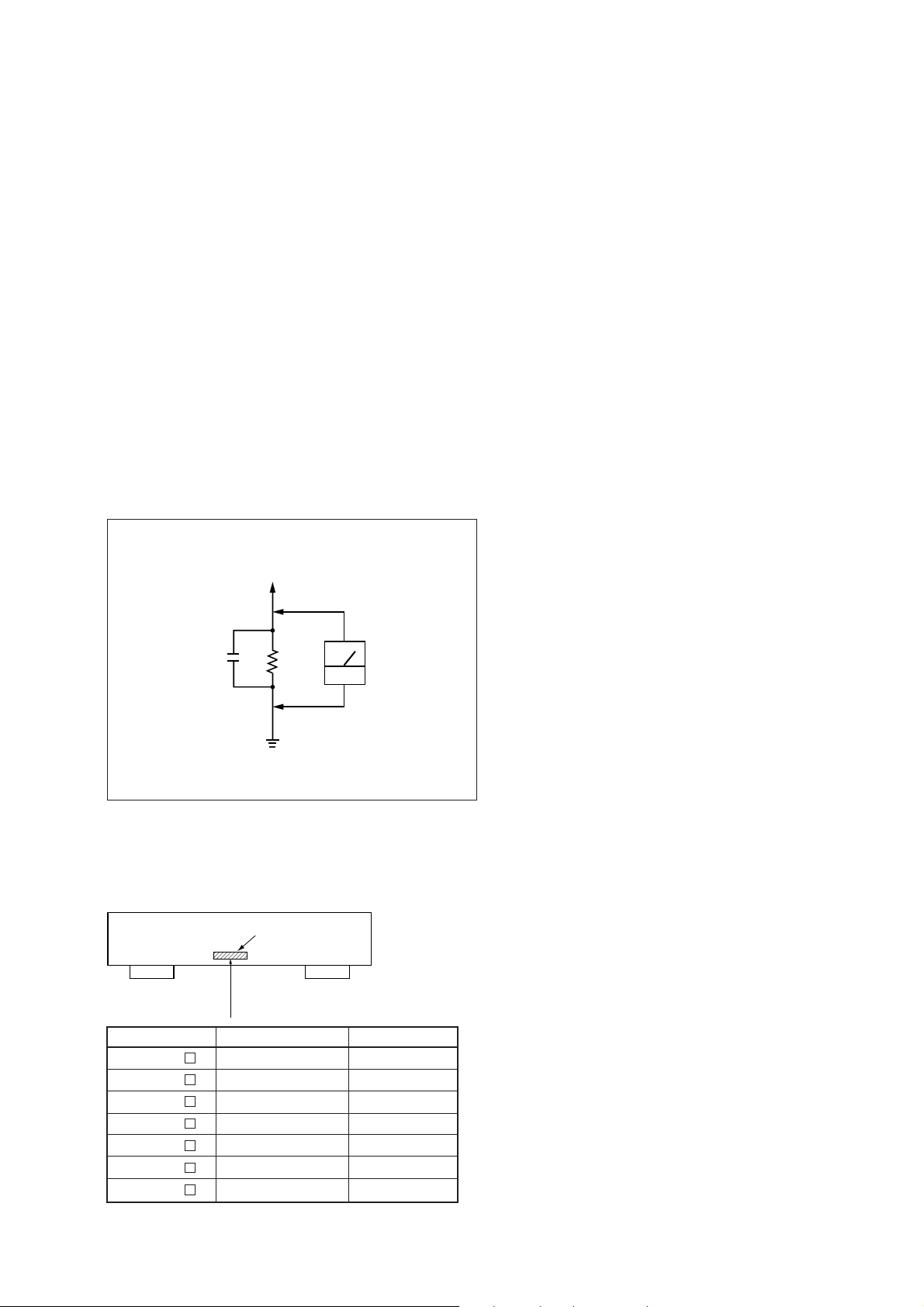
LEAKAGE
The AC leakage from any exposed metal part to earth Ground and
from all exposed metal parts to any exposed metal part having a
return to chassis, must not exceed 0.5 mA (500 microampers). Leakage current can be measured by any one of three methods.
1. A commercial leakage tester, such as the Simpson 229 or RCA
WT-540A. Follow the manufacturers’ instructions to use these
instruments.
2. A battery-operated AC milliammeter. The Data Precision 245
digital multimeter is suitable for this job.
3. Measuring the voltage drop across a resistor by means of a V OM
or battery-operated AC voltmeter. The “limit” indication is 0.75
V, so analog meters must have an accurate low-voltage scale.
The Simpson 250 and Sanwa SH-63Trd are examples of a passive VOM that is suitable. Nearly all battery operated digital
multimeters that have a 2V AC range are suitable. (See Fig. A)
To Exposed Metal
Parts on Set
0.15µF
1.5k
Ω
AC
voltmeter
(0.75V)
1. SERVICING NOTE
.......................................................... 5
2. GENERAL .......................................................................... 8
3. DISASSEMBLY
3-1. Front Panel ......................................................................... 22
3-2. Back Panel and Main Board ............................................... 23
3-3. Bracket (T), (L) and (R)...................................................... 24
3-4. BD Board ........................................................................... 24
3-5. SUB Chassis........................................................................ 25
3-6. Shutter Assembly ................................................................ 25
3-7. Over Write Head ................................................................. 26
3-8. Slider Complete Assembly.................................................. 27
4. TEST MODE ..................................................................... 28
5. ELECTRICAL ADJUSTMENTS ............................... 31
6. DIAGRAMS
6-1. Circuit Boards Location ...................................................... 36
6-2. Block Diagrams
• BD Section ....................................................................... 37
• Main Section .................................................................... 39
6-3. Printed Wiring Board — BD Section — ............................. 42
6-4. Schematic Diagram — BD Section — ............................... 45
6-5. Schematic Diagram — Main Section — ............................ 49
6-6. Printed Wiring Board — Main Section —.......................... 53
6-7. Schematic Diagram — Panel Section — ............................ 55
6-8. Printed Wiring Board — Panel Section — ......................... 57
6-9. IC Block Diagrams ............................................................. 60
6-10. IC Pin Functions ............................................................... 65
Earth Ground
Fig. A. Using an AC voltmeter to check AC leakage.
MODEL IDENTIFICATION
— BACK PANEL —
Parts No.
Parts No. Model
4-989-525-1
4-989-525-2
4-989-525-3
4-989-525-4
4-989-525-5
4-989-525-6
4-989-525-7
US model
Canadian model
AEP model
UK model
Singapore model
Hong Kong model
Tourist model
Product country
MALAYSIA
MALAYSIA
MALAYSIA
MALAYSIA
MALAYSIA
MALAYSIA
JAPAN
7. EXPLODED VIEWS
7-1. Main Section ....................................................................... 74
7-2. Front Panel Section ............................................................. 75
7-3. Mechanism Deck Section (1) (MDM-3B) .......................... 76
7-4. Mechanism Deck Section (2) (MDM-3B) .......................... 77
8. ELECTRICAL PARTS LIST ........................................ 78
— 3 —
SECTION 1
SERVICING NOTE
JIG FOR CHECKING BD BOARD WAVEFORM
The special jig (J-2501-124-A) is useful for checking the waveform of the BD board. The names of terminals and the checking items to be
performed are shown as follows.
I+3V : For measuring IOP (Check the deterioration of the optical pick-up laser)
IOP : For measuring IOP (Check the deterioration of the optical pick-up laser)
TEO : TRK error signal (Traverse adjustment)
VC : Reference level for checking the signal
RF : RF signal (Check jitter)
RF
VC
TEO
IOP
I + 3V
Jig
(J-2501-124-A)
CN110
FORCED RESET
The system microprocessor can be reset in the following way.
Use these methods when the unit cannot be operated normally due to the overrunning of the microprocessor, etc.
Method :
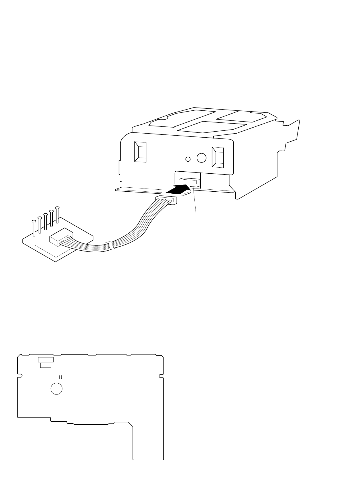
Disconnect the power plug, short-circuit JW143 and JW164 on the main board with a pincette or etc.
[MAIN BOARD] (Component Side)
Mechanism deck
S301
CN302
JW143
C001
JW164
— 4 —

RETRY CAUSE DISPLAY MODE
• In this test mode, the causes for retry of the unit during recording can be displayed on the fluorescent display tube.
This is useful for locating the faulty part of the unit.
• The data amount stored in D RAM, number of retries, and retry cause are displayed. Each is displayed in hexadecimal number.
• The display of the D RAM data amount enables data reading, accumulation, ejection, and writing to be performed smoothly. If wr iting is
not smooth, data may decrease considerably.
Method:
1. Load a recordable disc whose contents can be erased into the unit.
2. Press the EDIT/NO button several times to display “All Erase?” on the fluorescent display tube.
3. Press the YES button.
4. When “All Erase??” is displayed on the fluorescent display tube, the numbers on the music calendar will start blinking.
5. Press the YES button to display “Complete”, and press the p button immediately and continue pressing for about 10 seconds.
6. When the “TOC” displayed on the fluorescent display tube goes off, release the p button.
7. Press the r button to start recording.
8. Press the DISPLAY/CHAR button to display the test mode (Fig. 1), and check the display.
9. The Rt value increases with each retry. If an error occurs after a retry, “Retry Error” will be displayed, and the number of retries counted
will be set back to 0.
10. To exit the test mode, press the POWER button. Turn OFF the power, and after “TOC” disappears, disconnect the power plug from the
outlet.
Fig. 1 Reading the Test Mode Display
SC @@ Rt # # ∗ ∗
Fluorescent Display Tube Signs
@@ : Displays the DRAM memory amount when at all times.
# # : Displays the number of retries. When a retry error occurs, the number will be set back to 0.
* * : Cause of retry
All three displays above are in hexadecimal numbers.
— 5 —
Reading the Retry Cause Display
Higher Bits Lower Bits
Hexadecimal
Bit
Binary
Reading the Display:
Convert the hexadecimal display into binary display. If more than two causes, they will be added.
Example
When 42 is displayed:
Higher bit : 4 = 0100 n b6
Lower bit : 2 = 0010 n b1
In this case, the retry cause is combined of “CLV unlock” and “ader5”.
84218421
b7 b6 b5 b4 b3 b2 b1 b0
00000000
00000001
00000010
00000100
00001000
00010000
00100000
01000000
10000000
Hexa-
decimal
00
01
02
04
08
10
20
40
80
Cause of Retry Occurring conditions
Spindle is slow
(Not used)
ader5
Discontinuous address
(Not used)
FCS incorrect
IVR rec error
CLV unlock
Access fault
When spindle rotation is detected as slow
(Not used)
When ADER was counted more than
five times continuously
When ADIP address is not continuous
(Not used)
When not in focus
When ABCD signal level exceeds the specified range
When CLV is unlocked
When access operation is not performed normally
When A2 is displayed:
Higher bit : A = 1010 n b7+b5
Lower bit : 2 = 0010 n b1
The retry cause in this case is combined of “access fault”, “IVR rec error”, and “ader5”.
Hexadecimal n Binary Conversion Table
Hexadecimal Binary Hexadecimal Binary
0
1
2
3
4
5
6
7
0000
0001
0010
0011
0100
0101
0110
0111
8
9
A
B
C
D
E
F
1000
1001
1010
1011
1100
1101
1110
1111
— 6 —
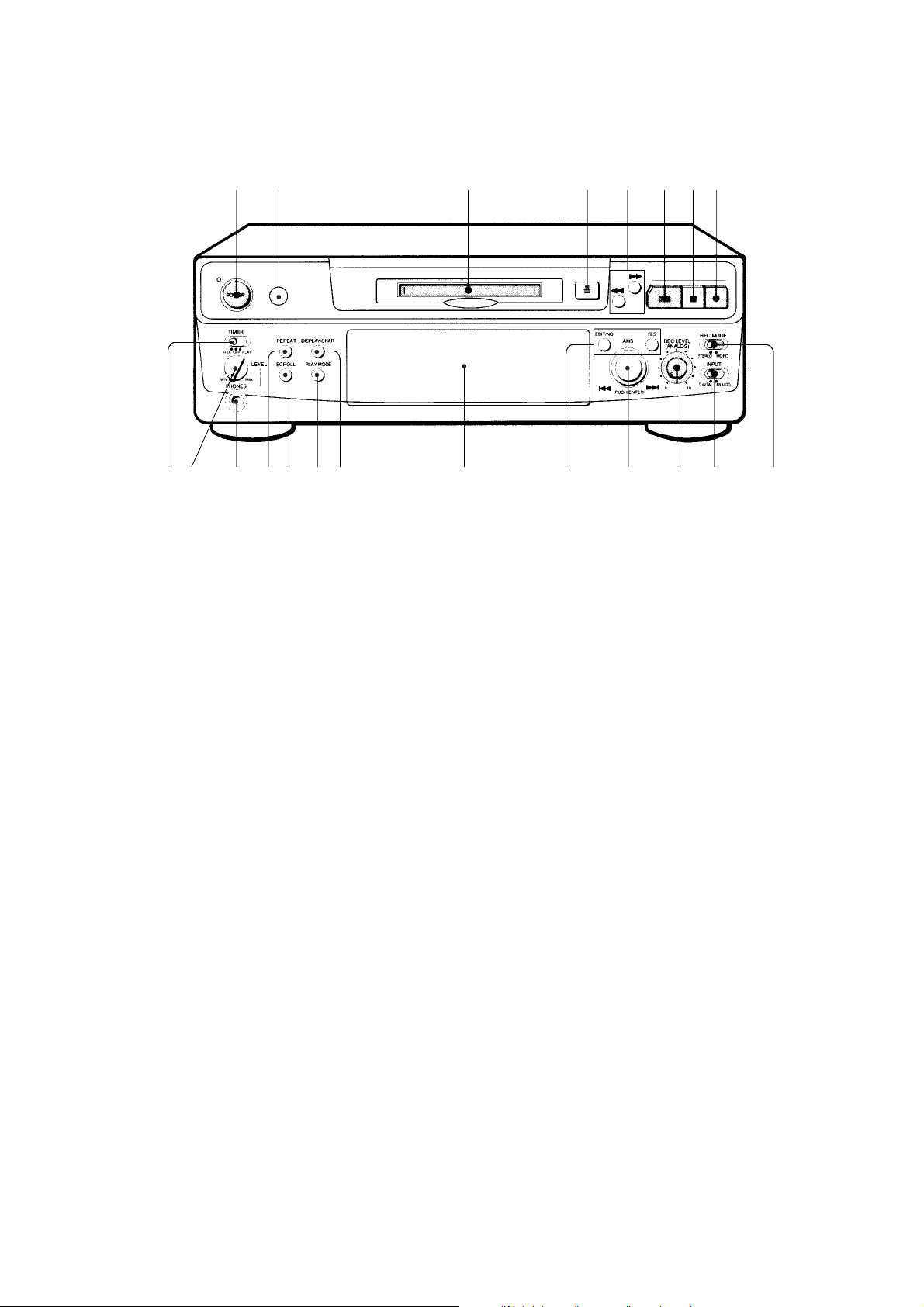
Location of Parts and Controls
SECTION 2
GENERAL
213567
18 17 1516192021
1 POWER switch
2 Remote sensor
3 Disc compartment
4 § (eject) button
5 0/) (fast backward/fast forward) buttons
6 fl (play/pause) button
7 p (stop) button
8 r (recording) button
9 REC MODE switch
10 INPUT switch
14
48
13
11 REC LEVEL (ANALOG) knob
12 AMS knob
13 EDIT/NO/YES buttons
14 Display window
15 DISPLAY/CHAR button
16 PLAY MODE button
17 SCROLL button
18 REPEAT button
19 PHONES jack
20 PHONES LEVEL knob
21 TIMER switch
12
10
911
— 7 —
This section is extracted from
instruction manual.
— 8 —
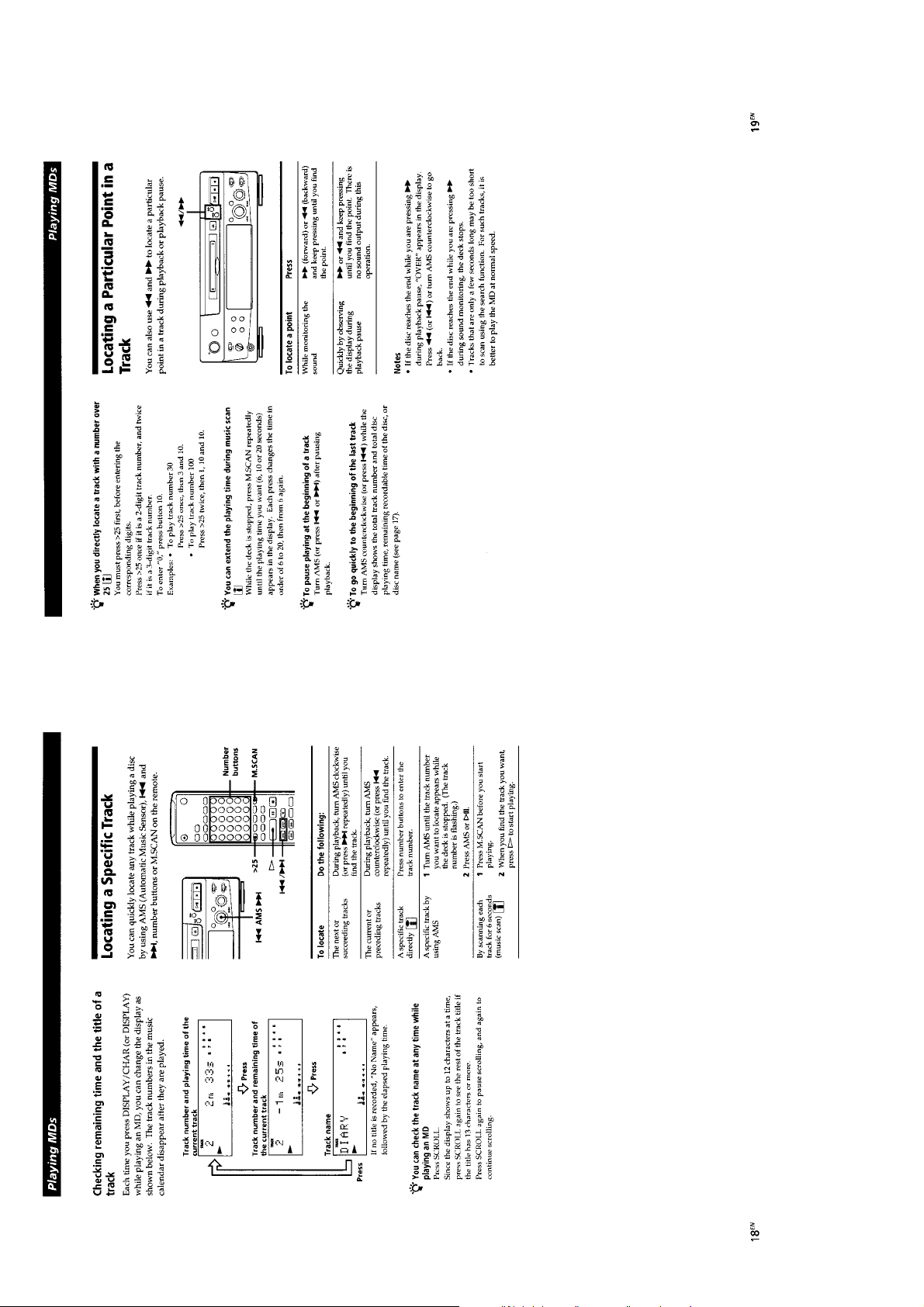
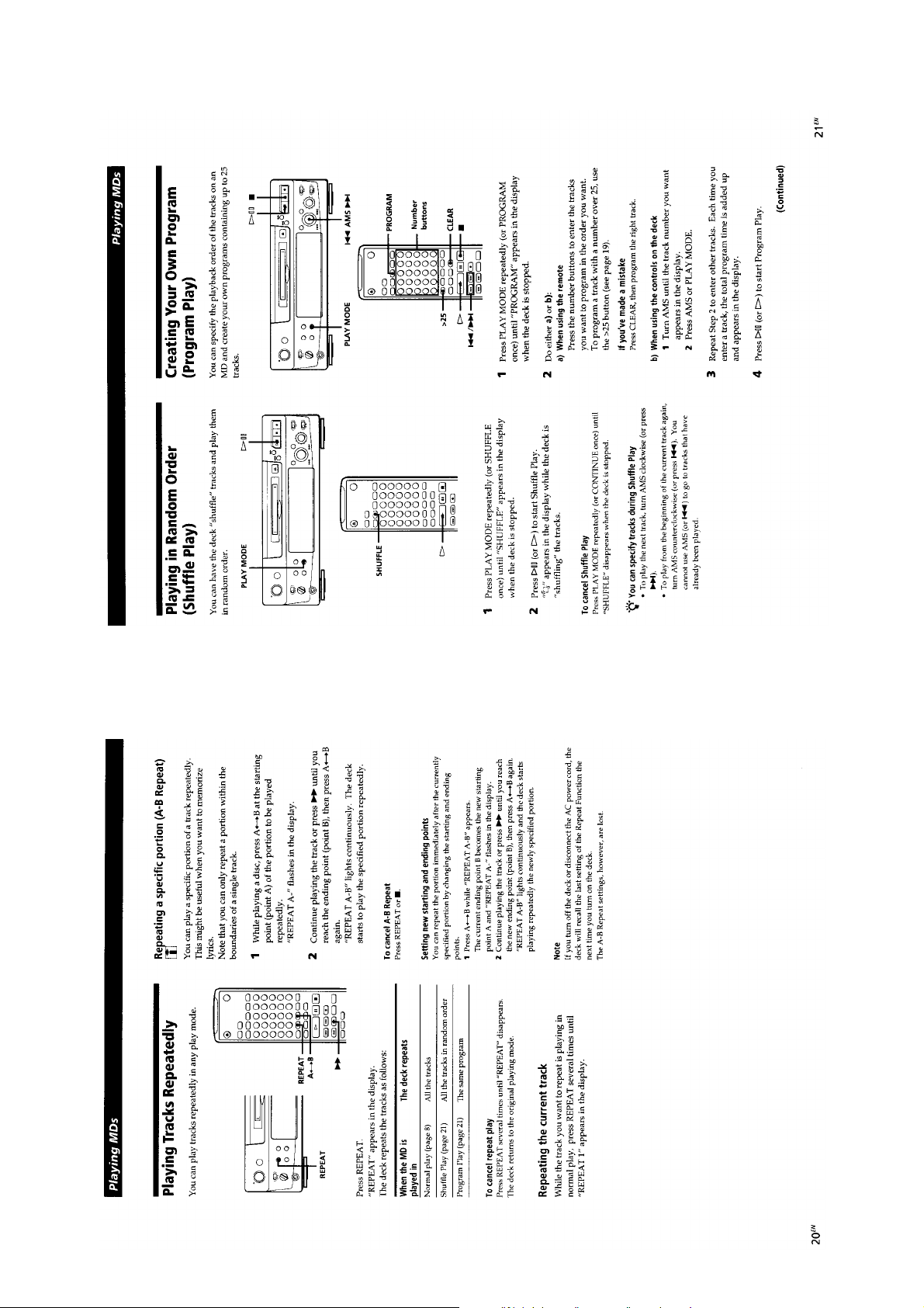
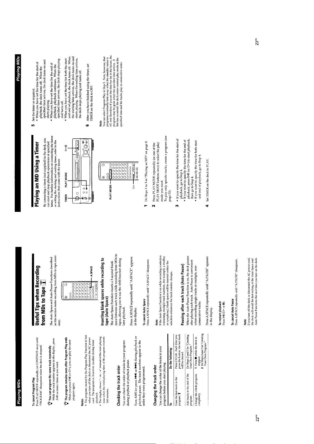
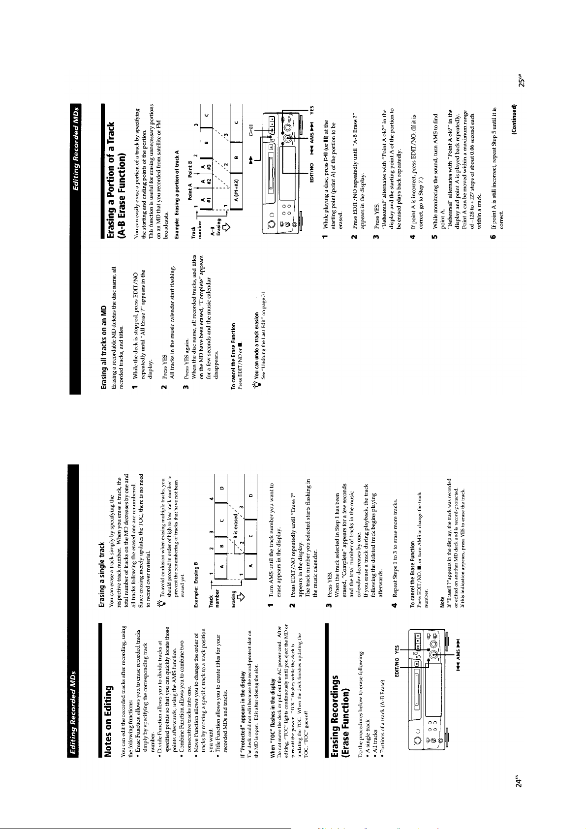
— 9 —
— 10 —
— 11 —
— 12 —
— 13 —
— 14 —
— 15 —
— 16 —
— 17 —
— 18 —
— 19 —
— 20 —
 Loading...