Sony KLV-30MR1 Schematic
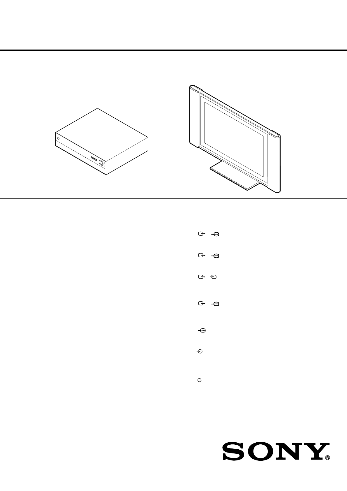
SERVICE MANUAL
SPECIFICATIONS
KLV-30MR1
AEP Model
Media Receiver Unit (MBT-MRL1)
Power Requirement: 220-240V AC; 50/60 Hz
Power Consumption: 30 W
Standby Power Consumption: 0.6 W
Dimensions (w x h x d):
Approx. 430 x 105 x 360 mm
Weight: Approx. 6 kg
Display Unit (LDM-3000)
Power Requirement: 220-240V AC; 50/60 Hz
Screen Size: 30inches
Approx. 76 cm measured
diagonally
Display Resolution:
1280 dots (horizontal) x 768 lines
(vertical)
Power Consumption: 150 W
Standby Power Consumption: 0.1W
Dimensions (w x h x d):
Approx. 974 x 530 x 95 mm
Weight: Approx. 20 kg
Approx. 27 kg (including stand)
Panel System:
LCD Display Panel
TV system:
Depending on your country selection:
B/G/H, D/K, L, I
Colour system:
PAL, SECAM
NTSC 3.58, 4.43 (only Video In)
Aerial:
75 ohm external terminal for VHF/UHF
Channel Coverage:
VHF: E2-E12
UHF: E21-E69
CATV: S1-S20
HYPER: S21-S41
D/K: R1-R12, R21-R69
L: F2-F10, B-Q, F21-F69
I: UHF B21-B69
Rear Terminals:
1/
21-pin Scart connector (CENELEC
standard) including audio/video input,
RGB input, TV audio/video output.
2/
21-pin Scart connector (CENELEC
standard) including audio/video input,
RGB input, TV audio/video output.
S
3/ (SMARTLINK; selectable)
21-pin Scart connector (CENELEC
standard) including audio/video input, S
video input, selectable audio/video
output and Smartlink interface.
4/ (SMARTLINK; selectable)
21-pin Scart connector (CENELEC
standard) including audio/video
input, RGB input, selectable audio/
video output, and Smartlink interface.
5
Y: 1 Vp-p, 75 ohms, 0.3V negative sync
P
B: 0.7 Vp-p, 75 ohms
P
: 0.7 Vp-p, 75 ohms
R
5
audio input (phono jacks)
500 m Vrms (100% modulation),
Impedance: 47 kilo ohms
5555
SUB WOOFER: phono jack
: audio outputs (Left/Right) - phono jacks
5555
CENTRE SPEAKER IN:
15 W x 2 (4-ohms)
CTRL S: minijack
AV MOUSE: minijack
LCD COLOR TELEVISION
Front Terminals:
S
6
S video input (4-pin mini DIN):
Y: 1 Vp-p, 75-ohms unbalanced, sync
negative
C: 0.286 Vp-p (Burst signal), 75 ohms
6
video input (phono jack):
1 Vp-p, 75-ohms unbalanced, sync
negative
6
audio input (phono jacks):
500 m Vrms (100% modulation),
Impedance: 47 kilo ohms
headphones jack
i
PC
PC Input (15-Dsub)
G: 0.7 Vp-p, 75 ohms, non Sync on Green
B: 0.7 Vp-p, 75 ohms, non Sync on Green
R: 0.7 Vp-p, 75 ohms, non Sync on Green
HD:1-5 Vp-p
VD:1-5 Vp-p
PC
PC audio input: minijack
Memory Stick Slot
Sound Output:
10 W x 2
Accessories supplied:
• One Remote Control (RM-972)
• Two size AAA batteries (R03 type)
• One Display Interface Cable
• One Coaxial Cable
• One AV Mouse
• Two Mains Leads (Type C-4)
• Two Mains Leads (Type BF)
• Two Mains Leads (Type C-5)
Main leads Type BF and Type C-5
may not be supplied depending on
the country.
Other features:
• Teletext, Fastext, TOPtext
• Sleep Timer
• Smartlink (direct link between your TV set
and a compatible VCR. For more
information on Smartlink, please refer to the
Instruction Manual of your VCR).
It's available either
(Selectable)
• TV system Autodetection
• Auto Format
3 or
4.
PC Input Timing:
Input signal frequency
Horizontal: 15.6 - 90 kHz
Vertical: 48 - 85 Hz
Maximum Resolution: 1600 dots x 1200 lines
KLV-30MR1(AEP) 2
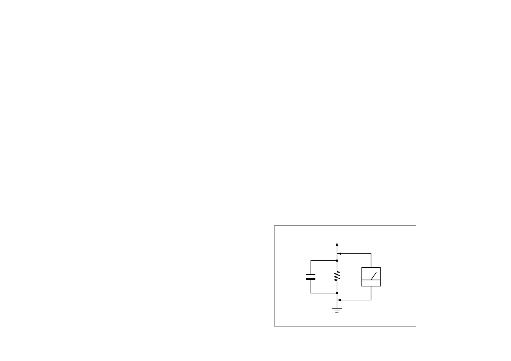
1.5 k
Ω
0.15 µF
AC
Voltmeter
(0.75 V)
To Exposed Metal
Parts on Set
Earth Ground
SAFETY CHECK-OUT
After correcting the original service problem, perform the following safety
checks before releasing the set to the customer:
1. Check the area of your repair for unsoldered or poorly-soldered
connections. Check the entire board surface for solder splashes and
bridges.
2. Check the interboard wiring to ensure that no wires are “pinched” or
contact high-wattage resistors.
3. Check that all control knobs, shields, covers, ground straps, and
mounting hardware have been replaced. Be absolutely certain that you
have replaced all the insulators.
4. Look for unauthorized replacement parts, particularly transistors, that
were installed during a previous repair. Point them out to the customer
and recommend their replacement.
5. Look for parts which, though functioning, show obvious signs of
deterioration. Point them out to the customer and recommend their
replacement.
6. Check the line cords for cracks and abrasion. Recommend the
replacement of any such line cord to the customer.
7. Check the connector shell, metal trim, “metallized” knobs, screws, and
all other exposed metal parts for AC Leakage. Check leakage as described right.
LEAKAGE TEST
The AC leakage from any exposed metal part to earth ground and from all
exposed metal parts to any exposed metal part having a return to chassis,
must not exceed 0.5 mA (500 microamperes).
Leakage current can be measured by any one of three methods.
1. A commercial leakage tester, such as the Simpson 229 or RCA WT540A. Follow the manufacturers’ instructions to use these instruments.
2. A battery-operated AC milliammeter. The Data Precision 245 digital
multimeter is suitable for this job.
3. Measuring the voltage drop across a resistor by means of a VOM or
battery-operated AC voltmeter. The “limit” indication is 0.75 V, so
analog meters must have an accurate low-voltage scale. The Simpson 250
and Sanwa SH-63Trd are examples of a passive VOMs that are suitable.
Nearly all battery operated digital multimeters that have a 2 V AC range
are suitable. (See Fig. A)
Fig. A. Using an AC voltmeter to check AC leakage.
KLV-30MR1(AEP) 3

WARNING!!
AVERTISSEMENT!!
SAFETY-RELATED COMPONENT WARNING!!
COMPONENTS IDENTIFIED BY SHADING AND MARK ! ON THE
SCHEMATIC DIAGRAMS, EXPLODED VIEWS AND IN THE
PARTS LIST ARE CRITICAL FOR SAFE OPERATION. REPLACE
THESE COMPONENTS WITH SONY PARTS WHOSE PART
NUMBERS APPEAR AS SHOWN IN THIS MANUAL OR IN
SUPPLEMENTS PUBLISHED BY SONY. CIRCUIT ADJUSTMENTS THAT ARE CRITICAL FOR SAFE OPERATION ARE
IDENTIFIED IN THIS MANUAL. FOLLOW THESE PROCEDURES
WHENEVER CRITICAL COMPONENTS ARE REPLACED OR IMPROPER OPERATION IS SUSPECTED.
ATTENTION AUX COMPOSANTS RELATIFS À LA SÉCURITÉ!!
LES COMPOSANTS IDENTIFIÉS PAR UNE TRAME ET UNE
MARQUE ! SONT CRITIQUES POUR LA SÉCURITÉ. NE LES
REMPLACER QUE PAR UNE PIÈCE PORTANT LE NUMÉRO
SPECIFIÉ. LES RÉGLAGES DE CIRCUIT DONT L’IMPORTANCE EST
CRITIQUE POUR LA SÉCURITÉ DU FONCTIONNEMENT SONT
IDENTIFIÉS DANS LE PRÉSENT MANUEL. SUIVRE CES
PROCÉDURES LORS DE CHAQUE REMPLACEMENT DE
COMPOSANTS CRITIQUES, OU LORSQU’UN MAUVAIS
FONCTIONNEMENT EST SUSPECTÉ.
KLV-30MR1(AEP) 4
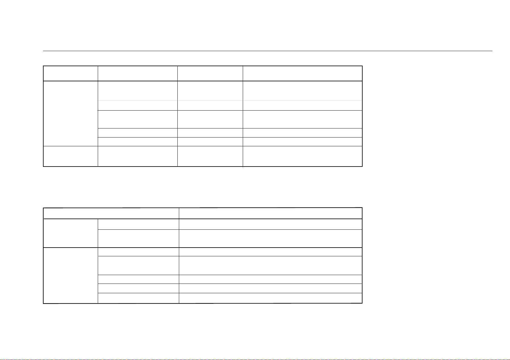
DIAGNOSIS (Reliability Self Diagnostic Display Specifications for MEDIA RECEIVER)
The abnormal conditions are indicated by the following LED flashes.
LED Status MEDIABOX PANEL
POWER/STBY • ⇔ • flashes alternately - PANEL ALARM
(Not available for re-start)
Flashes (1Hz) - Defective for cable connection
•Flashes four times - Defective for power voltage of fan,
fan protection
•Flashes six times +3.3V malfunction Power protection on G board detected
•Flashes nine times PANEL malfunction TIMER Flashes (1Hz) Defective for cable -
connection
This unit has the following self diagnostic function. Refer to this table to
identify a defective point in case of any malfunction.
Problem Symptom
Mediabox Digital 3.3V malfunction Shut down when Digital 3.3V becomes equal or under 0V.
Defective for cable The both White and Black interface cables are not connected
connection with the panel.
Panel PANEL ALARM
Defective for cable The both White and Black interface cables are not connected
connection with the MEDIABOX.
Fan malfunction
Power protector operation
*Operation count is based on WDT.
*For flashes, the Power/Standby LED flashes in red.
*The flash period is based on the reliability standard.
KLV-30MR1(AEP) 5

TABLE OF CONTENTS
Section Title Page Section Title Page
1. DISASSEMBLY ....................................................... 1-1
1-1. Display Unit (LDM-3000) ................................... 1-1
1-1-1. Stand and Cabinet Removal ...................... 1-1
1-1-2. G and P Boards Removal........................... 1-2
1-1-3. K Board Removal...................................... 1-3
1-1-4. R1 and R2 Boards Removal ...................... 1-4
1-1-5. Panel Support Assy (LCD Panel) .............. 1-5
1-1-6. LCD Panel Removal.................................. 1-6
1-2. Media Receiver Unit (MBT-MRL1) .................... 1-7
1-2-1. Panel and Covers Removal........................ 1-7
1-2-2. G2, A, and MS Boards Removal .............. 1-8
1-2-3. TU Board Removal.................................... 1-9
1-2-4. U Board Removal ..................................... 1-10
1-2-5. H2 Board Removal .................................... 1-11
1-2-6. H5 Board Removal ................................... 1-12
1-2-7. MSX Board Removal ................................ 1-13
1-2-8. H1 Board Removal ................................... 1-14
1-2-9. H4 Board Removal .................................... 1-15
2. TROUBLESHOOTING ........................................... 2-1
2-1. Display Unit (LDM-3000) .................................... 2-1
2-2. Media Receiver Unit (MBT-MRL1)..................... 2-2
3. DIAGRAMS ............................................................... 3-1
3-1. Block Diagrams .................................................... 3-1
3-1-1. Display Unit(LDM-3000).......................... 3-1
3-1-2. Media Receiver Unit (MBT-MRL1) ........ 3-5
3-2. Frame Diagram ..................................................... 3-14
3-3. Circuit Boards Location ........................................ 3-15
3-3-1. Display Unit(LDM-3000).......................... 3-15
3-3-2. Media Receiver Unit (MBT-MRL1) ......... 3-15
3-4. Schematic Diagrams and Printed WiringBoards... 3-15
3-4-1. Display Unit(LDM-3000).......................... 3-16
(1)Schematic Diagrams of G Board ..................... 3-16
(2)Schematic Diagram of K Board ...................... 3-18
(3)Schematic Diagrams of P Board ..................... 3-20
(4)Schematic Diagrams of R1 amd R2 Boards .... 3-26
KLV-30MR1(AEP) 6

Section Title Page Section Title Page
3-4-2. Media Receiver Unit (MBT-MRL1) ......... 3-27
(1)Schematic Diagrams of A Board ..................... 3-27
(2)Schematic Diagram of G2 Board .................... 3-40
(3)Schematic Diagrams of H1 Board ................... 3-42
(4)Schematic Diagram of H2 Board .................... 3-44
(5)Schematic Diagrams of H4 and H5 Boards ..... 3-46
(6)Schematic Diagrams of MS Board .................. 3-47
(7)Schematic Diagram of MSX Board ................. 3-51
(8)Schematic Diagrams of TU Board .................. 3-52
(9)Schematic Diagrams of U Board ..................... 3-55
3-5. Semiconductor ...................................................... 3-58
4. EXPLODED VIEWS .............................................. 4-1
4-1. Display Unit (LDM-3000) ................................... 4-2
5. ELECTRICAL PARTS LIST ............................... 5-1
4-2. Media Receiver Unit (MBT-MRL1) .................... 4-4
4-3.
Packing Materials for Display Unit (LDM-3000)
... 4-6
4-4. Packing Materials for Media Receiver Unit
(MBT-MRL1) ..................................................... 4-7
KLV-30MR1(AEP) 7
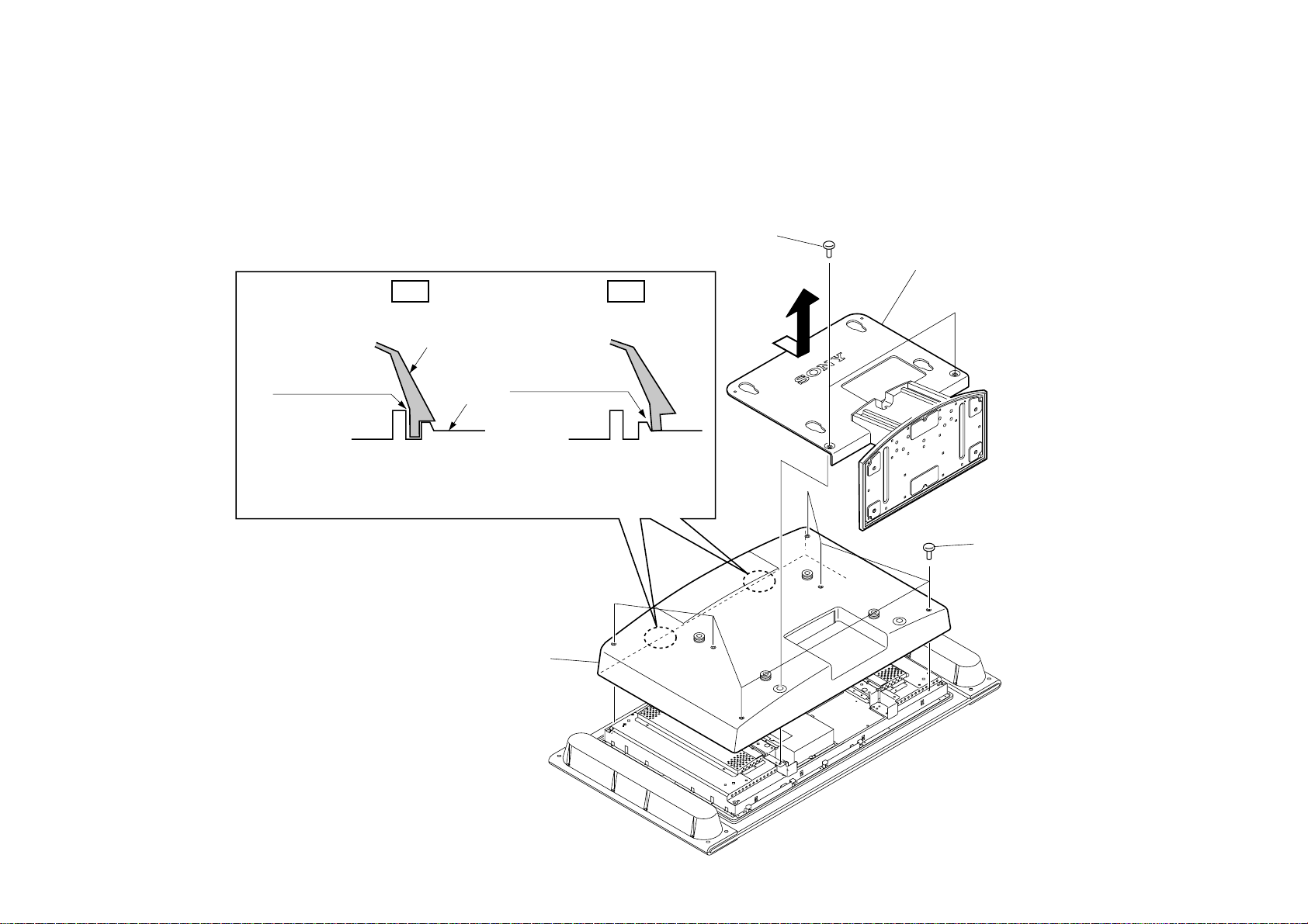
1-1. DISPLAY UNIT (LDM-3000)
1-1-1. STAND AND CABINET REMOVAL
Assembly
Fit in the groove
Note:
Ensure that the top side of Cabinet assy is fit
in the groove of the bezel completely.
OK
Cabinet
Bezel
SECTION 1
DISASSEMBLY
1 Two screws
(+PSW 5X14)
2 Stand assy
NG
Cabinet assy defects
from the groove
4 Cabinet assy
3 Six screws
(+B 4X6)
KLV-30MR1(AEP) 1-1
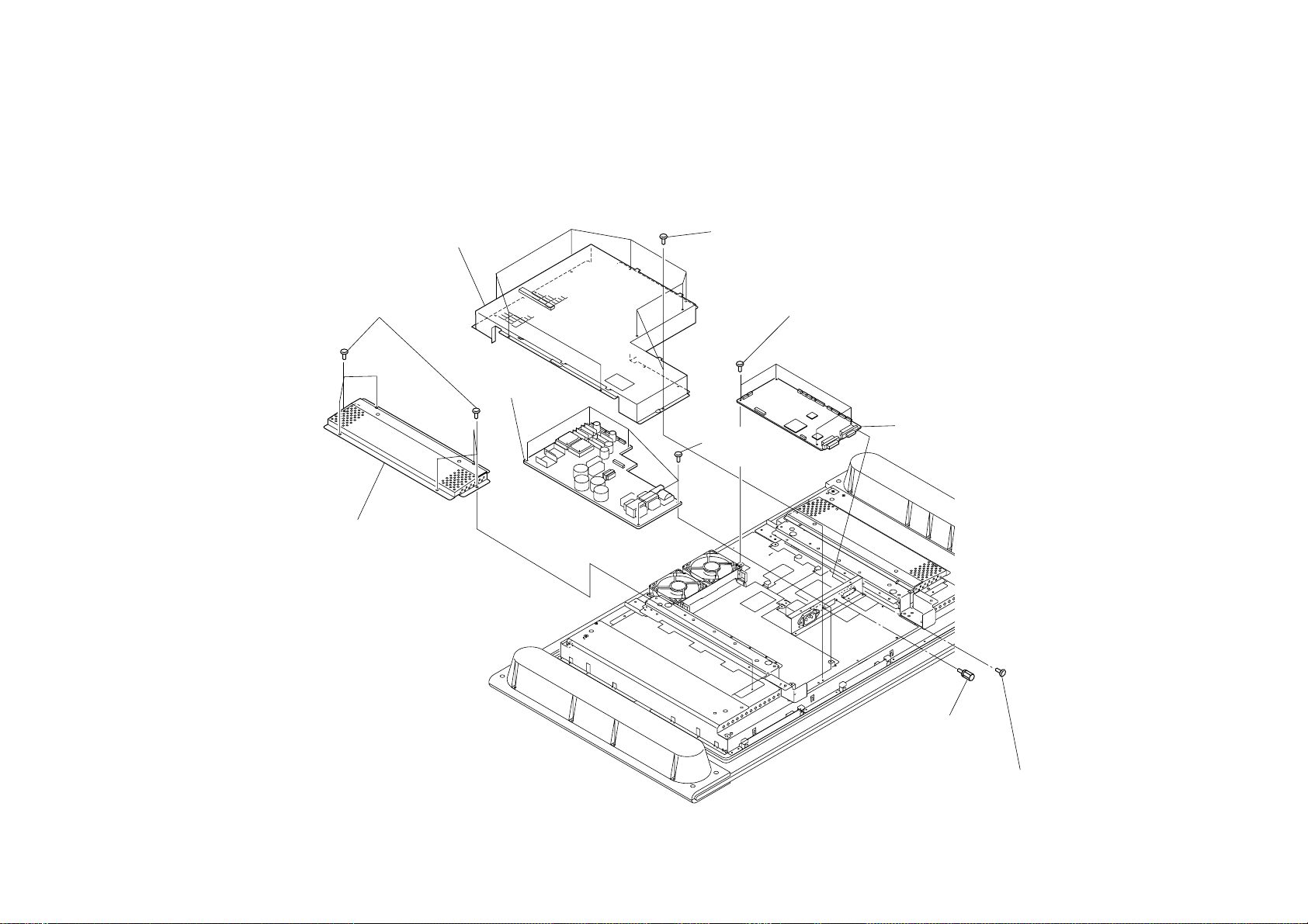
1-1-2. G AND P BOARDS REMOVAL
4 EMI shield center
1 Six screws
(+BVTT 3X6)
2 EMI shield side
3 Nine screws
(+BVTT 3X6)
7 Four screws
(+BVTT 3X6)
6 G Board
0 P Board
5 Five screws
(+BVTT 3X6)
8 Two screws (HEX)
9 Two screws
GRIP, M2.6 S HEAD (EG)
KLV-30MR1(AEP) 1-2
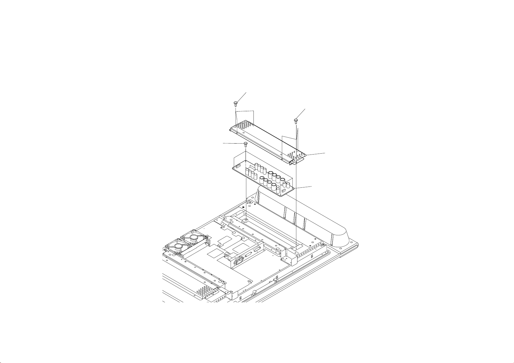
1-1-3. K BOARD REMOVAL
1 Three screws
(+BVTT 3X6)
1 Three screws
(+BVTT 3X6)
3 Four screws
(+BVTT 3X6)
2 EMI shield side
4 K Board
KLV-30MR1(AEP) 1-3
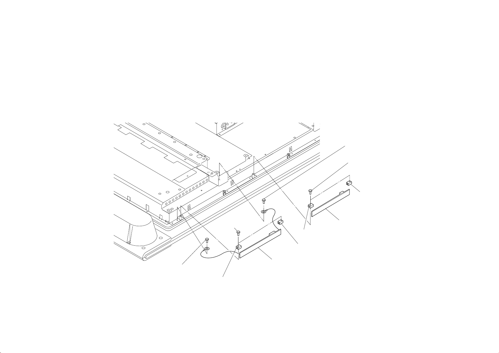
1-1-4. R1 AND R2 BOARDS REMOVAL
5 Two screws
(+BVTP 3X12)
2 R Board bracket
6 R Board bracket
6 R Board bracket
2 R Board bracket
7 R2 Board
4 R1 Board
1 Two screws
(+BVTP 3X12)
3 Screws
(+BVTP 4X10)
3 Screw
(+BVTP 4X10)
KLV-30MR1(AEP) 1-4
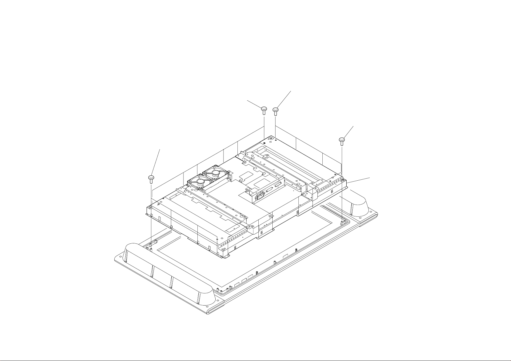
1-1-5. PANEL SUPPORT ASSY (LCD PANEL)
1 Four screws
(+BVTP 4X10)
1 Six screws
(+BVTP 4X10)
1 Four screws
(+BVTP 4X10)
1 Six screws
(+BVTP 4X10)
2 Panel support assy
(LCD panel)
KLV-30MR1(AEP) 1-5
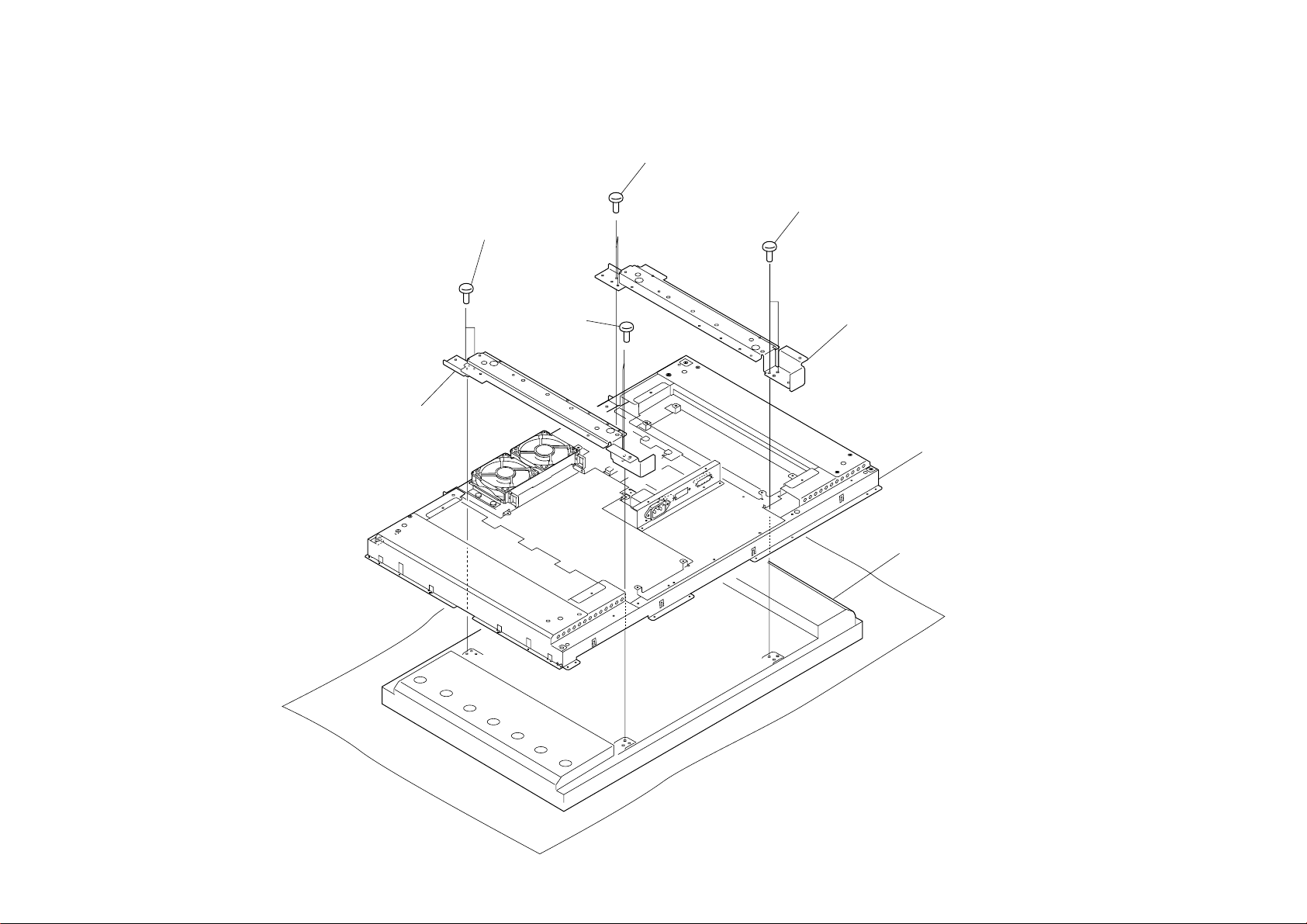
1-1-6. LCD PANEL REMOVAL
4 Main arm (R)
3 Two screws
(+PS 4X6)
3 Two screws
(+PS 4X6)
1 Two screws
(+PS 4X6)
1 Two screws
(+PS 4X6)
2 Main arm (L)
5 Panel support assy
6 LCD panel
KLV-30MR1(AEP) 1-6
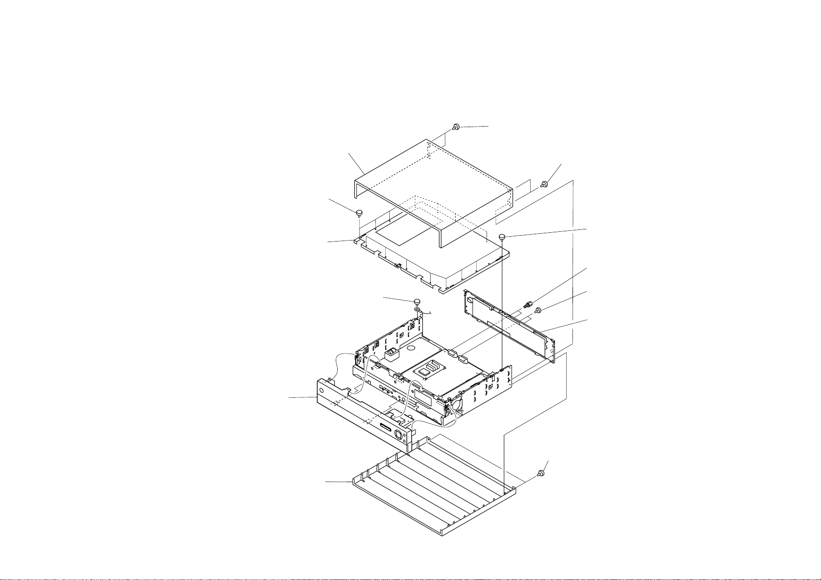
1-2. MEDIA RECEIVER UNIT (MBT-MRL1)
1 Two screws
(M3, SW)
6Two screws
(M3, SW)
0 Rear panel
7 Bottom cover assy
!¡ Front panel assy
1 Two screws
(M3, SW)
3 Eight screws
(Precision)
5 Screw
(+PSW 4X8)
3 Nine screws
(Precision)
2 Top cover
4 Top plate
9 Two screws
(M3, SW)
8 Two Connector screws
1-2-1. PANEL AND COVERS REMOVAL
KLV-30MR1(AEP) 1-7
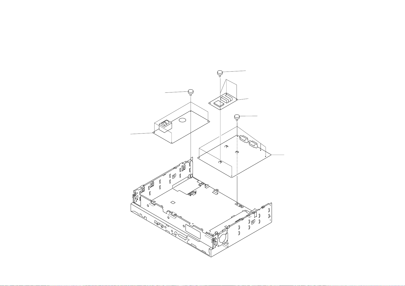
1-2-2. G2, A, AND MS BOARDS REMOVAL
5 Four screws
(M 3X8)
6 G2 Board
1 Three screws
(+BVTT 3X8)
2 MS Board
3 Five screws
(M 3X8)
4 A Board
KLV-30MR1(AEP) 1-8
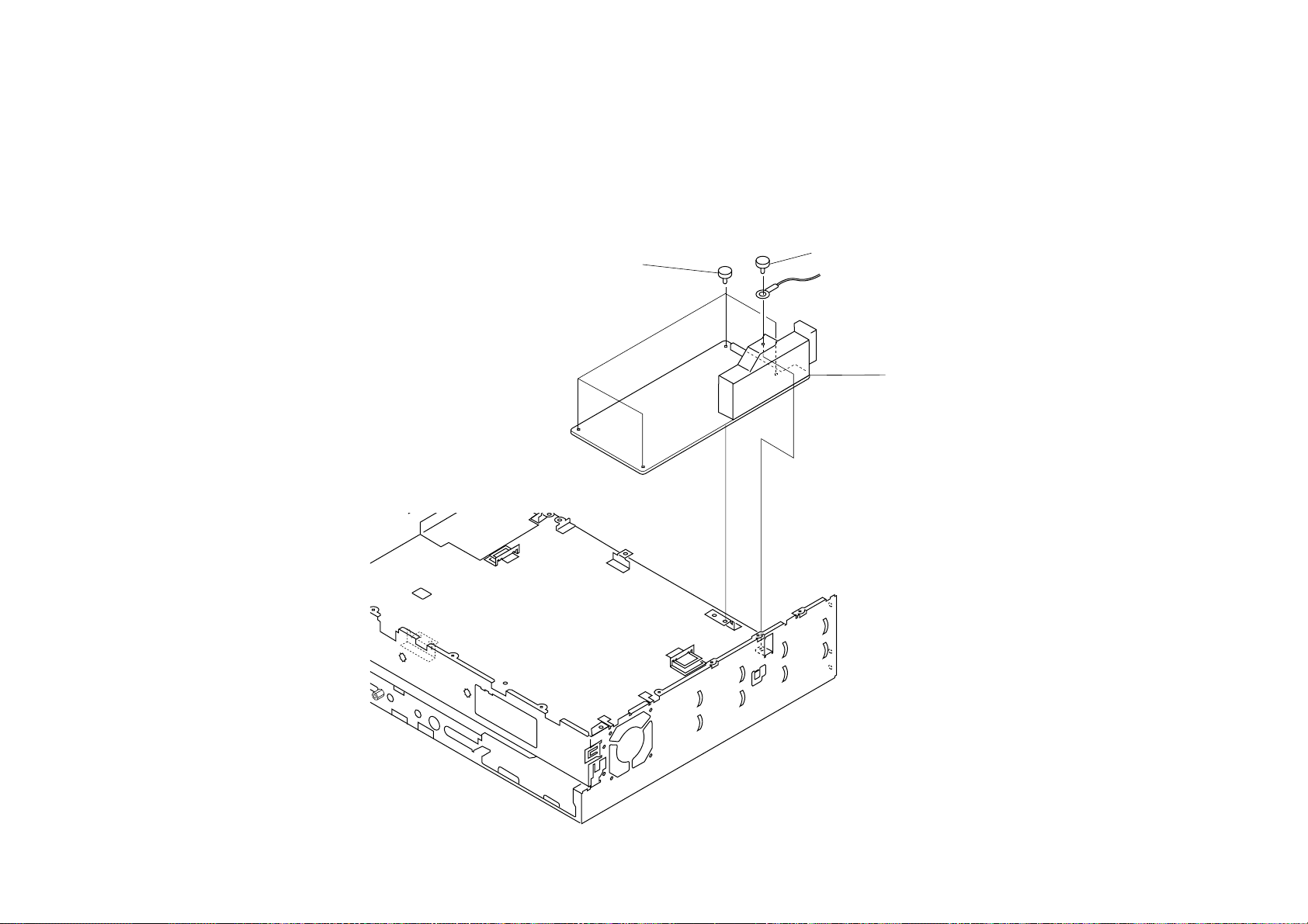
1-2-3. TU BOARD REMOVAL
2 Four screws
(M 3X8)
1 Screw
(M 3X8)
3 TU Board
KLV-30MR1(AEP) 1-9
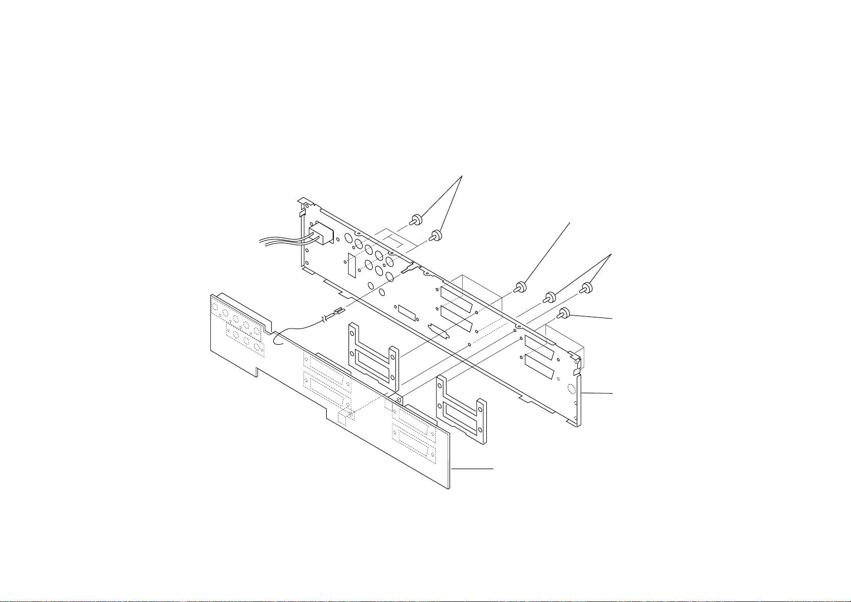
1-2-4. U BOARD REMOVAL
1 Four screws
(+BVTP 3X12)
1 Two screws
(+P 3X10)
2 Four screws
(+BVTT 4X14)
2 Four screws
(+BVTP 4X14)
3 U Board
Rear panel
KLV-30MR1(AEP) 1-10
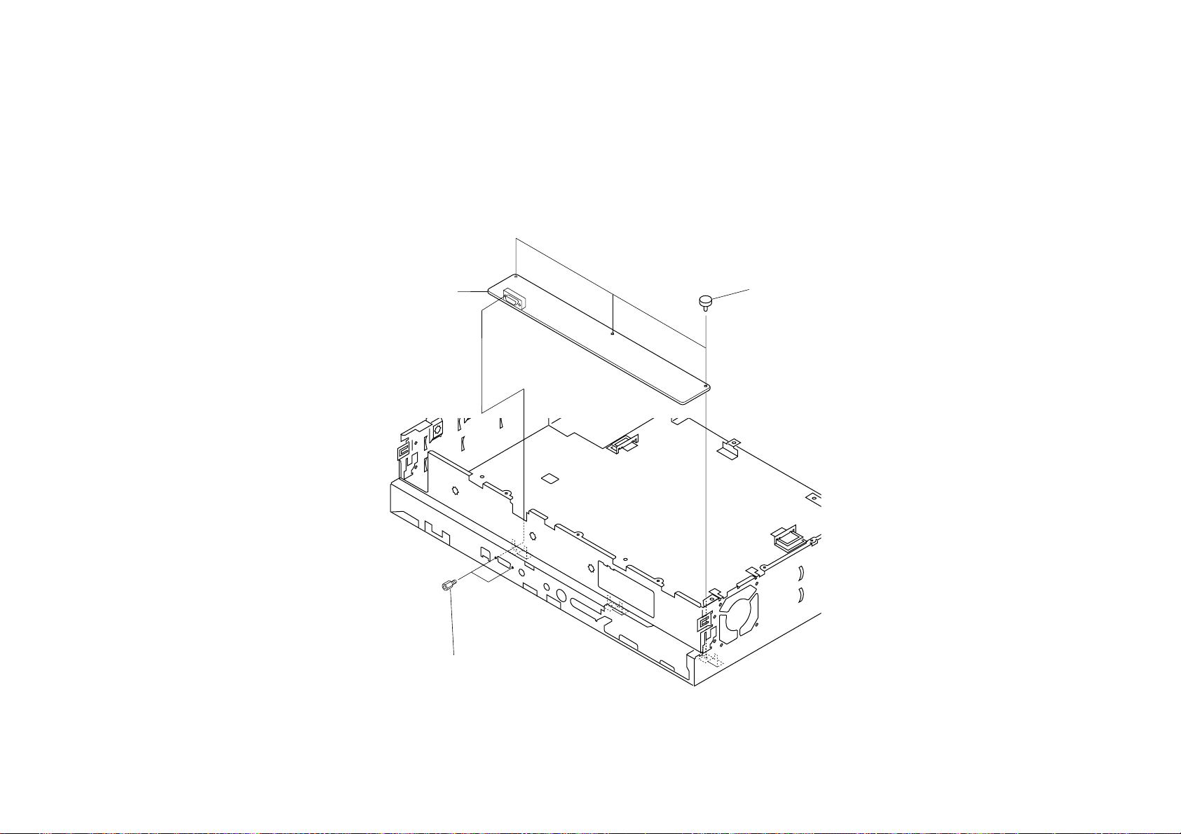
1-2-5. H2 BOARD REMOVAL
3 H2 Board
1 Three screws
(M 3X8)
2 Two connector screws
KLV-30MR1(AEP) 1-11
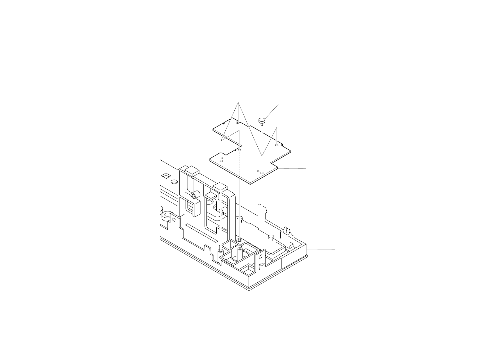
1-2-6. H5 BOARD REMOVAL
1 Five screws
(+BVTP 3X10)
2 H5 Board
Front panel
KLV-30MR1(AEP) 1-12
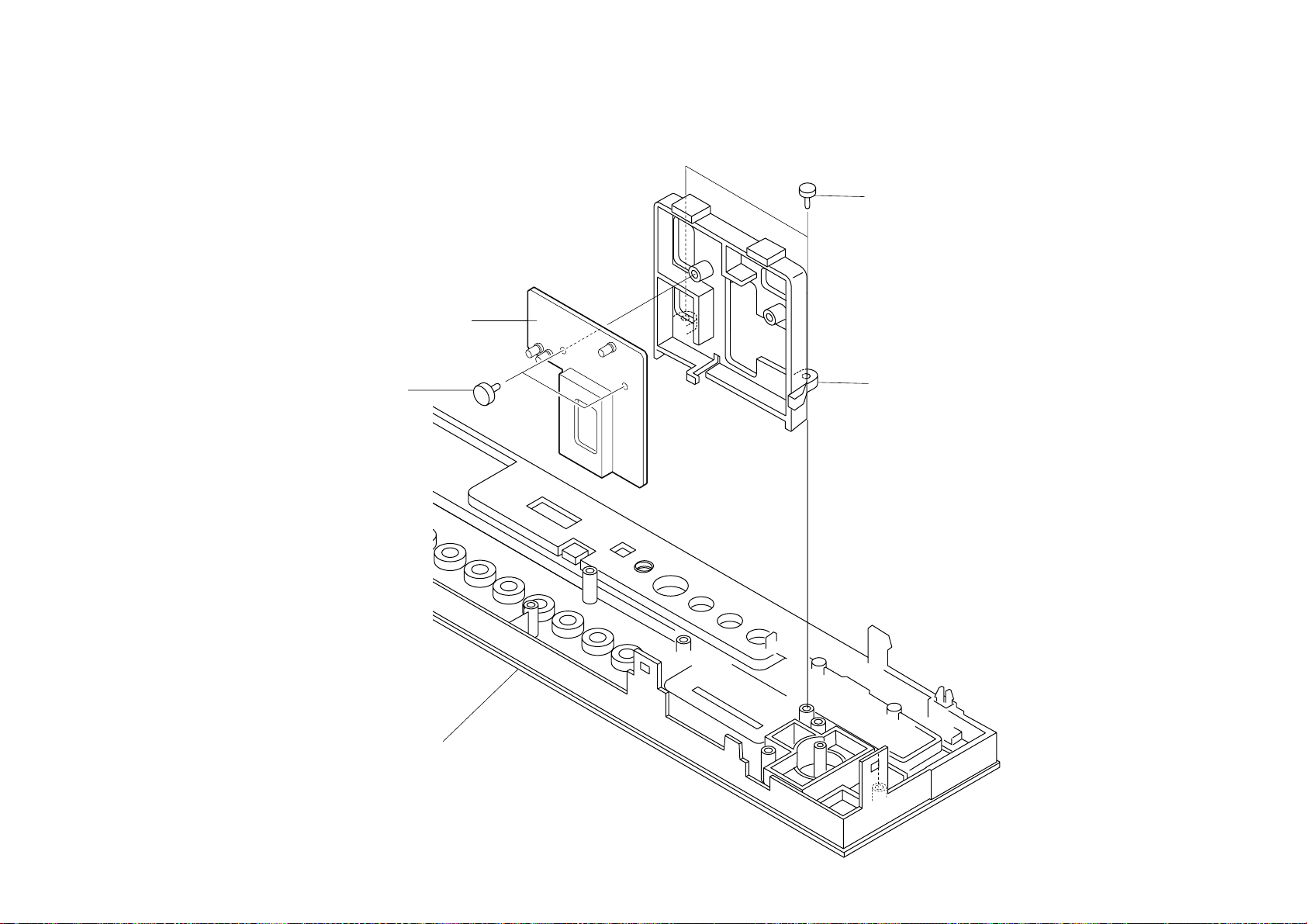
3 Two screws
(+BVTP 3X10)
1 Two screws
(+BVTP 3X12)
4 MSX Board
2 MS bracket
Front panel
1-2-7. MSX BOARD REMOVAL
KLV-30MR1(AEP) 1-13
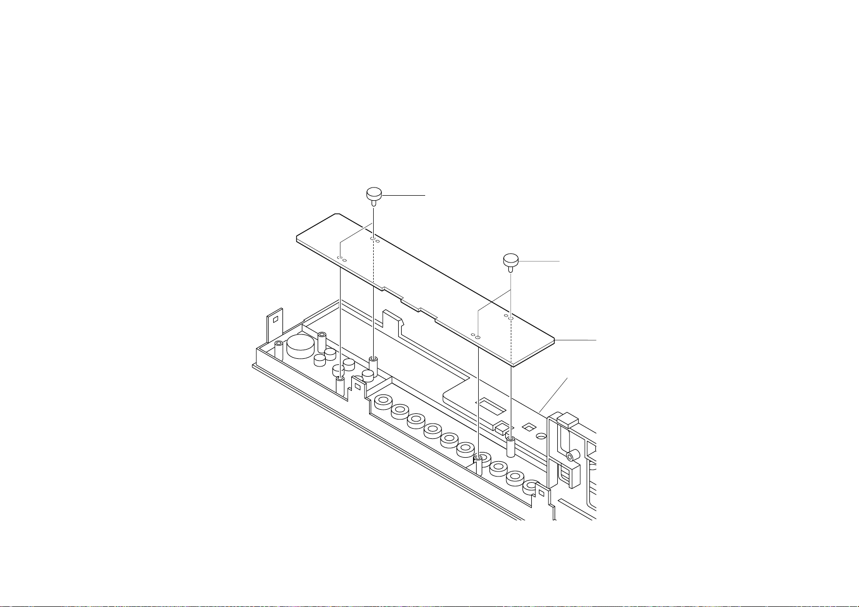
1-2-8. H1 BOARD REMOVAL
1 Two screws
(+BVTP 3X12)
1 Two screws
(+BVTP 3X12)
2 H1 Board
Front panel
KLV-30MR1(AEP) 1-14
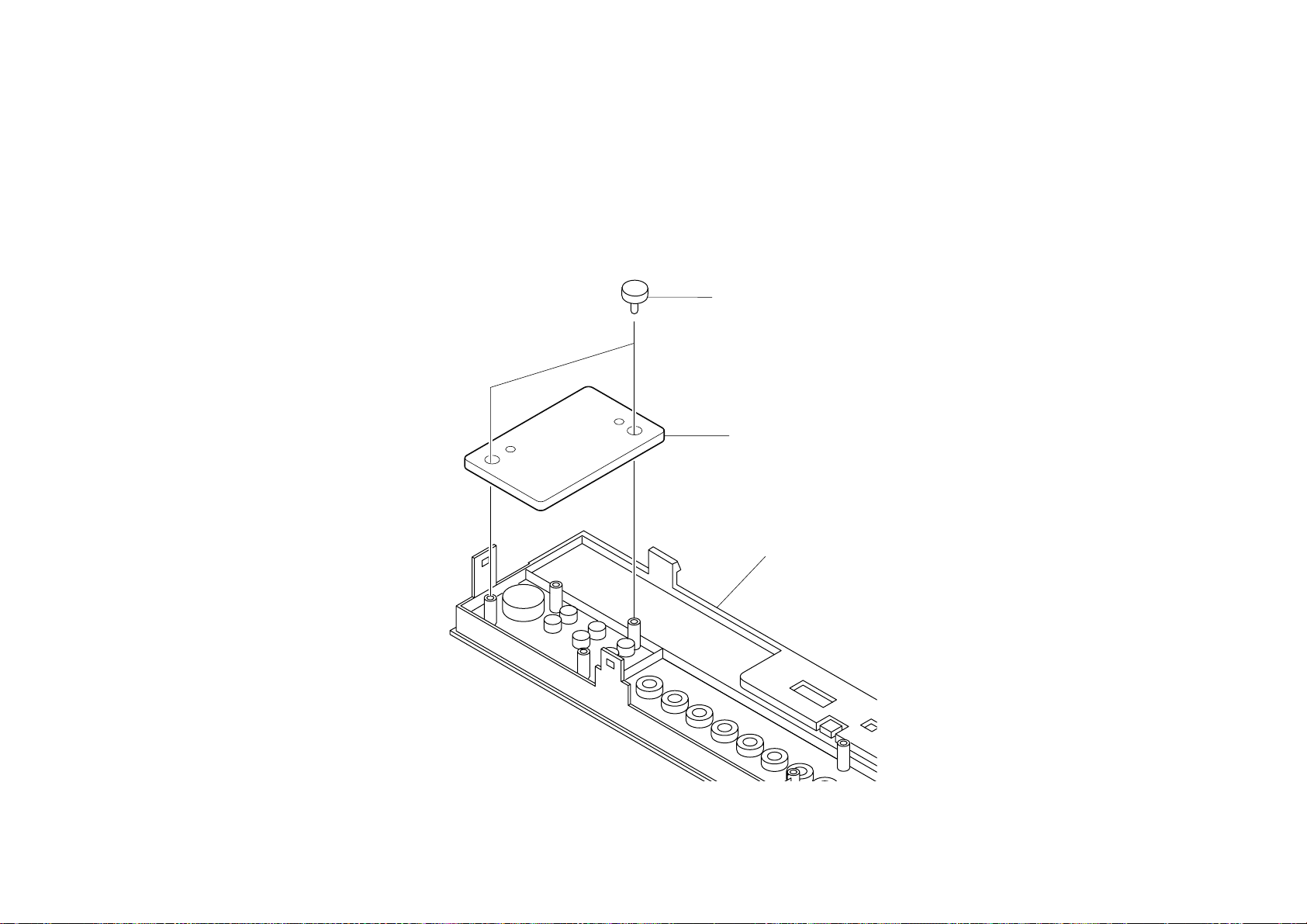
1-2-9. H4 BOARD REMOVAL
1 Two screws
(+BVTP 3X12)
2 H4 Board
Front panel
KLV-30MR1(AEP) 1-15
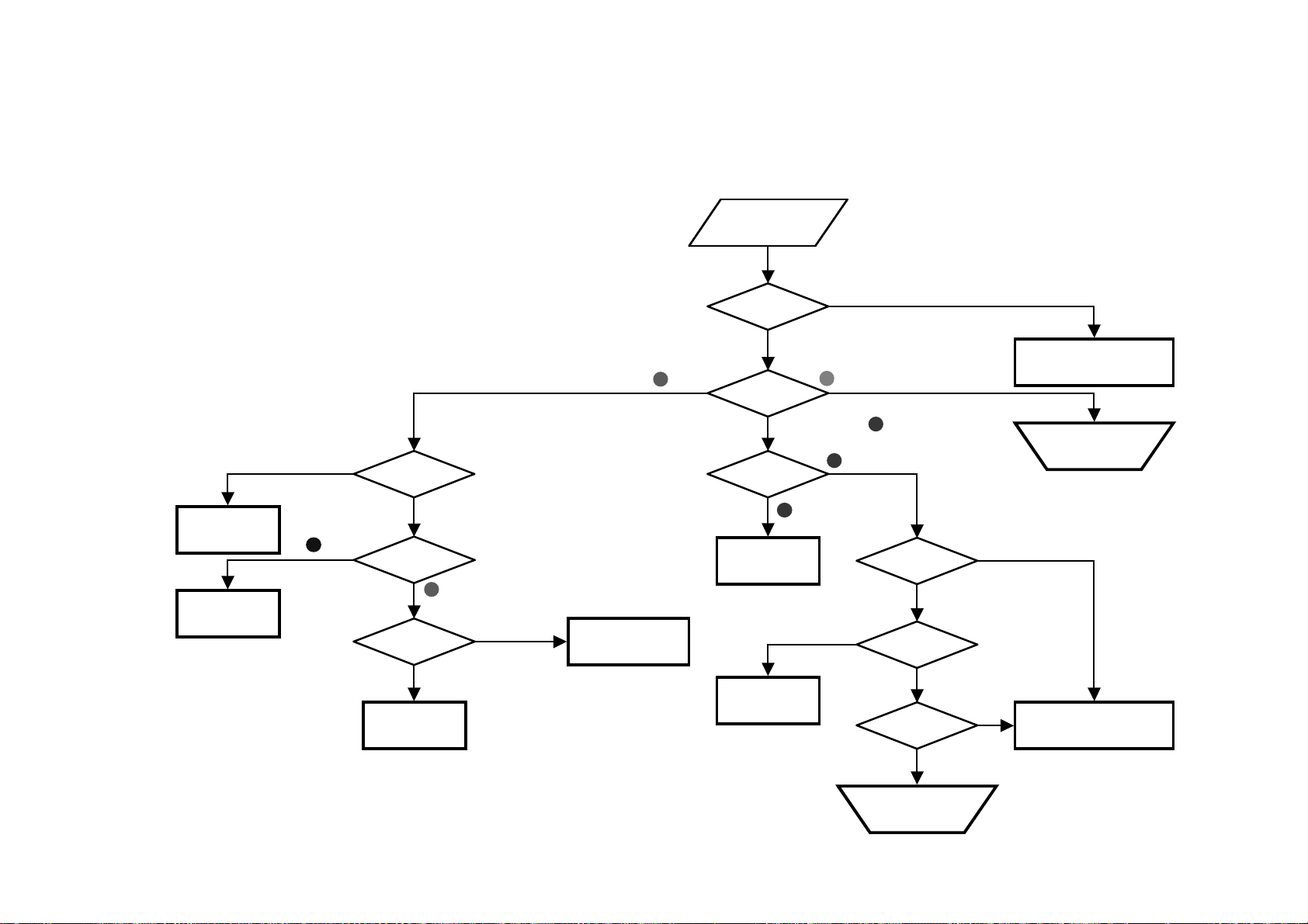
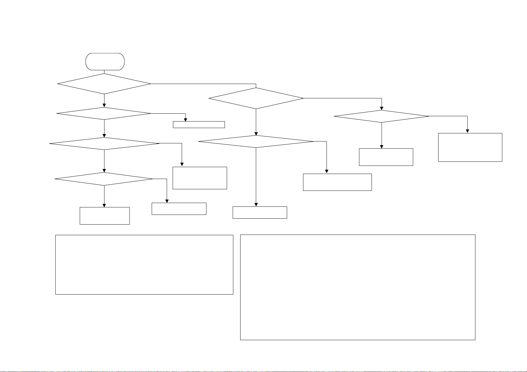
2-1. DISPLAY UNIT (LDM-3000)
SECTION 2
TROUBLESHOOTING
No image
appears.
Abnormal
Box failure
Image erasure
mode
Box LED?
Lights.
LED display
Priming?
P board failure
All is normal.
Lights.
NO: No light
emission
YES: Light emission
Lights.
Panel module
failure
Just after
start?
YES: Not appear at all.
LED display
BOX LED Blinks nine times.
LED display
Blinks six times.
G board failure
Fan or
circuit failure
NO: Appears for a few seconds.
Encrypted authentication
Blinks.
Blinks four times.
Just after
YES
error of box or display
start?
NO
NO
Fan rotation?
YES
Installation
environment?
NG
OK
Temperature sensor
Check of cable
connection
or circuit failure
Environment
improvement
KLV-30MR1(AEP) 2-1
2-2. MEDIA RECEIVER UNIT (MBT-MRL1)
Sound not output
from display unit
No sound from both channels
for all input sources
YES
Audio Output terminal
OK
Subwoofer terminal
OK
Display Signal Out
terminal (Black)
OK
Probable cause
• Cable defect
• Defect of display unit
Note:
When the insertion of the headphone terminal is detected, the display unit and the woofer
terminal do not output the sound.
In this condition, when the volume operation is performed, the headphone icon is
displayed.
If the condition of small or no sound occurs for only one channel, perform the balance
adjustment beforehand:
Select [AUDIO ADJ.] and [BALANCE] in order from the menu display for each input
source.
NG
(Try to turn up volume)
(Check frequency component)
NO
NG
NG
(DC only)
• Check AK4114
• Check SN65LVDS1050
Check two CXA2069Q's
Surround-sound system turning on
• Center Speaker
Check switch circuit
• Check input of NJW1149
• Check AK4524
No sound from only one
channel for all input sources
YES
OK
• Check two CXA2069Q's
• Check input of NJW1149
Check of AK4524
No problem when around 3MHz of rectangular wave (3.3Vpp) is output from the 13-pin SDTO. (The rectangular wave
changes depending on the audio signal.)
For the analog system, check the inputs (2 and 3 pins) and the outputs (25 through 28 pins). The outputs of these
terminals change depending on the volume adjustments.
Check of AK4114
No problem when around 3MHz of rectangular wave (3.3Vpp) is output for the JL5003[SPDIF]. (The rectangular wave
changes depending on the audio signal.)
Check that 48KHz of rectangular wave (3.3Vpp) is supplied to the 24-pin LRCK. (Supply source: AK4524)
Check that 3.072MHz of rectangular wave (3.3Vpp) is supplied to the 26-pin BICK. (Supply source: AK4524)
NO
No sound for BS reception only
NG
• Check output of NJW1149
• Check AK4524 (Analog input)
• Possibility of display unit defect
YES
• Check input of NJW1149
• Check IF board
• Check B block
NO
Determine signal source of
defective input
• Check ground wave tuner
• Check external input terminal
• Check two CXA2069Q's
Check of Display Signal Out terminals (Black)
The output signal level is about 3.3Vpp when the Display Signal Out terminals are not connected to the display unit.
If the signals, SPDIF+/- and UART_O+/-, are output, no problem for the sending end.
(When the Display Signal Out terminals are connected to the display unit, the signal level is about 350mVpp since the
signal is terminated at display unit.)
For receiving ends (SIRCS input and UART input), the check can only be performed when the Display Signal Out
terminals are connected to the display unit.
KLV-30MR1(AEP) 2-2
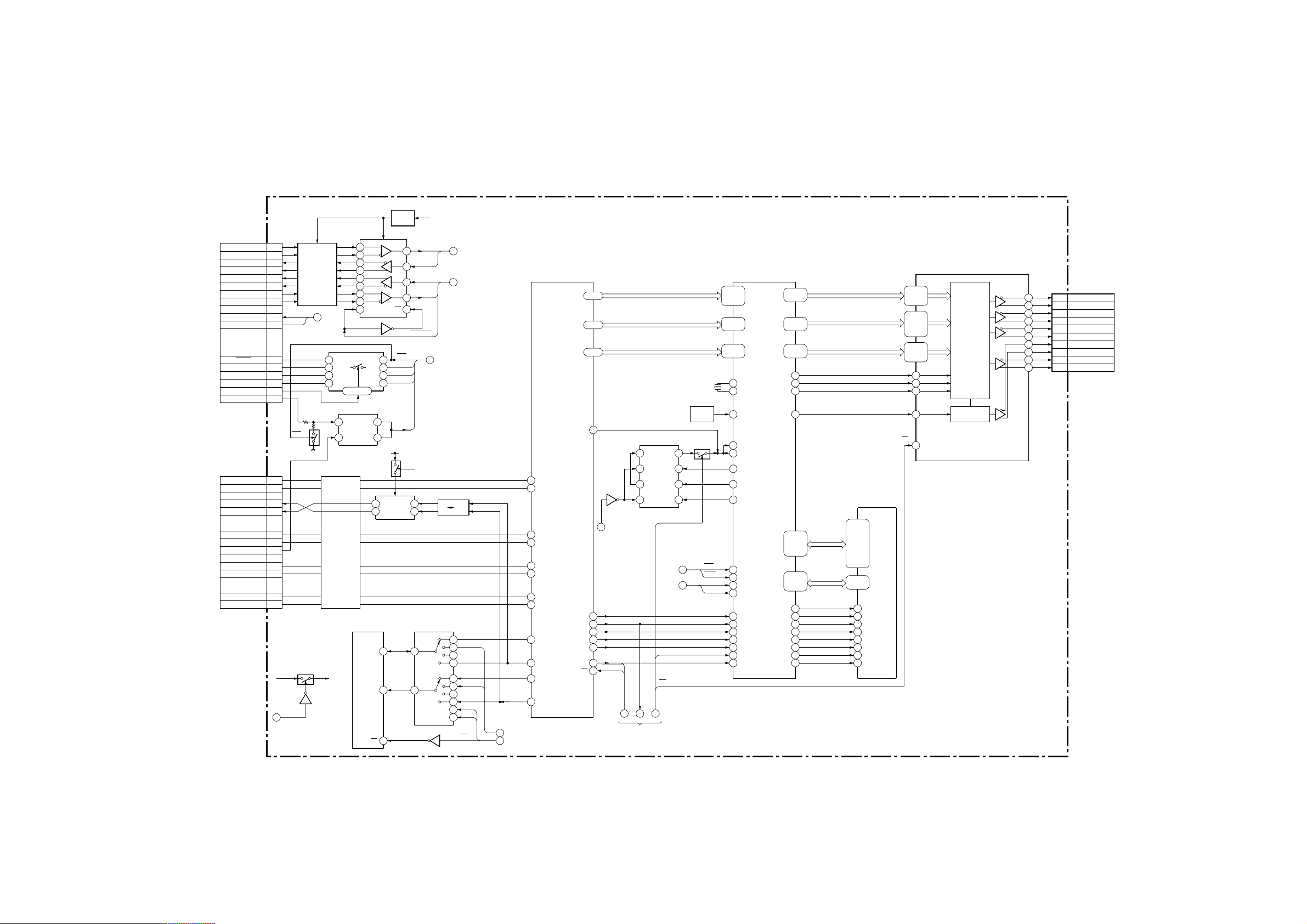
3-1. BLOCK DIAGRAMS
3-1-1. DISPLAY UNIT (LDM-3000)
CN3102
MD 1
JIG A7
CN3101
A13
A11
A10
D3111-D3114
A8
OVER VOLTAGE
A6
PROTECTOR
A4
A3
A1
STATUS
P SW
B5
B6
B7
1
2
6
7
10
14+5V POWER
16
18
23CLOCK+
24
+3.3V +3.3V
8
TO 2/2
TO 2/2
RES
Q3112
Q3113
TMDS ON
TO
MEDIA RECEIVER
UNIT
(BLACK)
TO
MEDIA RECEIVER
UNIT
(WHITE)
SPDIF-
SPDIF+
SIRCS-
SIRCS+
UART_O+
UART_O-
UART_I+
UART_I-
STATUS B3
POWER ON
RESET B11
TXD 1B8B9
RXD 1
CABLE DET
DATA 2-
DATA 2+
DDC SCL
DDC SDA
DATA 1- 9
DATA 1+
HOT PLUG DET
DATA 0- 17
DATA 0+
CLOCK-
SECTION 3
DIAGRAMS
Q3101
3.2V
REG
IC3101
LVDS RXTX
11
1
1A
8
3A
4A
11
2A
4
3
5
D3104-3107
OVER VOLTAGE
PROTECTOR
TO
IC3105,
3106,
3107
13
14
10
11
12
IC3109
12 13
5
,,6,
IC3108
VOLTAGE
DET
1
2
6
7
DE RE
1B
3B
2B 3
IC3106
EEPROM
SDA
SCL
WC
Q3111
2
9
104B
1
7
5V-4
IIC2
7 BUFF
IC3102
5
6
7
3
15
9
5
4
RES
TXD1
RXD1
MD1
DETQ3102
Q3109,3110
3.3V
5V-4
SPDIF
SIRCS
TXD 0
RXD 0
PD LVDS
7
3
6
IC3105
13
3
Q3108
6
TO 2/2
TO 2/2
5
TO 2/2
Q3104
5V 3.3V
12
14
15
11
1
5
2
4
10
A
B
9
SDA2
SCL2
SEL0
SEL1
WP
TO 2/29
10 TO 2/2
IC3107
TMDS RECEIVER
RX2-
81
80 RX2+
RX1-84
RX1+
83
RX0-87
RX0+
86
RXC+
89
90 RXC-
PROM SDA96
DDC SDA
93
95
PROM SCL
92 DDC SCL
QE16-23 30-37
20-27QE8-15
10-17QE0-7
44
ODCK
TO 2/2
48
HSYNC
47
VSYNC
DE 46
42RSVD
41
CTL2
SCDT
8
PD
2
Q3303
15
SCDT
PD TMDS
RI0-RI7
GI0-GI7
BI0-BI7
12
10
6
9
HSI
VSI(VSO V6)
DEI
CTL3
CTL2
VSI(VSO V6)
12 13 4
TO 2/2
IC3301 PLL
VCO
VCO
IN
OUT
VCO
SEL
INH
PFD
FIN
OUT
PFD
FIN
INHAB
PLL CLK ON
TO 2/2
TO 2/2
FIELD BOLT
PD
IC3501
4,
14
28
27
30
31
32
TD0,1
TA0-5
TD2,3,
TA6,
TB0-4
TD4,5,
TB5,6,
TC0-3
TC5
TC4
TC6
CLK IN
PDWN
LVDS TRANSMITTER
TA-
48
18
47
17
46
16
45
15
42
14
41
13
40
12
39
11
38
10
37
9
TTL PARALLEL
TO
LVDS
PLL
TA+
TB-
TB+
TC-
TC+
TCLK-
TCLK+
TD-
TD+
(PANEL CPU)
CN3504
TCLK-
TCLK+
TA-
TA+
TB-
TB+
TC-
TC+
TD-
TD+
TO
LCD
PANEL
IC3401
LCD DRIVER
174,175
ITQE
178-182,
16-23
184
185-188,
ITQE
191-194
8-15
195-199,
ITQE OBLU
202-204
0-7
X3401
33MHz
X3402
100MHz
OSC
IC3302
3
1
2
4
5
CLR
2
MUTE
SCL1
14
SDA1
CLK3311
OSC33
14
121
CLKI00
166
CLKTMDS
42
CLK30
CLK SEL25
23
APLL
21
BPLL
CLX
2
5 ICBLK
8
ICSCL
9
ICSDA
167
ITHSYNC
ITVSYNC
168
ITDE
169
170
ITCTL3
ITCTL2
171
ITCTL1
172
ITSCDT
173
O6RED
0-7
O6GRN
0-7
0-7
6HS 55
OCLK
DQ
1-16
A
0-11
CLK RAM
OCKE
OWE
ORAS
OCAS
OLDQM
OUDQM
OCS
87-92,
98,99
75-78,
80-83
56,58,
62-66
536VS
DE
54
51
141,
143-146,
149-153,
156-161
100-104,
108-113,
115
127
129
135
132
133
136
134
128
DQ1-16
A0-11
RO0-7
GO0-7
BO0-7
VSO
HSO
DEO
CLKO
2,3,
5,6,
8,9,
11,12, D
39,40,
42,43,
45,46,
48,49
19-24,
27-32
35
34
17
16
14
36
18
IC3402
DRAM
0-15
A
0-11
CLK
CKE
WE15
RAS
CAS
LDQM
UDQM
CS
2,3,
50-52,
54-56
10-12,
15,16
18-20,
22-24
PD
6-8,
P(1/2)
KLV-30MR1(AEP) 3-1
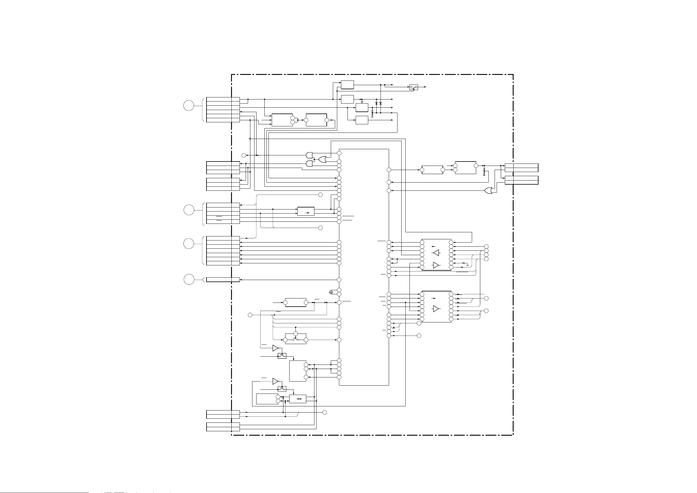
M
TO G BOARD
CN6303
LCD UNIT
BOARD
LCD UNIT
BOARD
N
TO K BOARD
CN3001
O
TO R1 BOARD
CN3202
P
TO R2 BOARD
CN3205
TO
TO
CN8001
24V
24V
STBY 6.5V
POWER ON
THERMO G
INV FAIL
CN3503
BR ON
BRTC
INV FAIL
CN3502
BR ON
BRTC
INV FAIL
CN3201
SPDIF
SDA2
SCL2
MUTE
RES
CN3202
SIRCS
MUTE
TIMER 2
TIMER 1
POWER
STBY
CN3204
LOGO 2
CN3209
SCL B
SDA B43
CN3206
SCL
SDA
1
2
5
7
8
10
5
3
1
5
3
1
3
6
7
9
10
2
4
5
6
7
8
9SAVING
TO 2/2
6
5
TO 1/2
15
SPDIF
SIRCS
7
TEMPERATURE
5V-4
RES
5V-4
CLR
3.3V
IC3211
SENSOR
IC8005
VOLTAGE
DET
POWER ON
BR ON
G PROT
LCD12 ON
24 DET
THERMO G
SDA2SCL2
5V-4
RES
TXD1
RXD1
MD1
DET
Q3205
Q3214
2
1
Q3204
Q3213
1
7
IC3201
7
3
Q3201
3.3V 5V
IC3202
IC3210
4
IC3204
EEPROM
SCL
SDA
WP
Q3203
3.3V 5V
SCL1
SDA1
IC8007
RESET
GEN
2
1
6
5
14.7456MHz
21
6
5
7
D3210
6
TO 1/2
9
TO 1/2
X3201
RES
24DET
45
14 TO 1/2
IC8004
+12V
REG
IC8003
+3.3V
REG
57
55
58
37
60
74
59
34
63
SDA2_0
SCL2_0
64
61
SDA2/1
SXL2_1
62
65
AU MUTE
66
AU RES
68
LED MUTE
69
LED TIMER 2
LED TIMER 1
70
LED POWER
71
LED STBY
72
SAVING
67
LED LOGO46
XTAL
2
3 EXTAL
1 RESET54RESET
TXD1
78
79
RXD1
MD1
4
CABLE DET20
51
SCL1 0
SCL1 1
49
SDA1 1
48
SDA1 0
50
42
WP1
IC8006
+5V
REG
IC8001
+5V
REG
IC3203
PANEL MCU
G PROT
DRV
FAN VCC
FAN ERR
ALARM 28
VSYNC
SCDT
RXDO
WAKEUP
C STATUS
TXDO
PD2 21
CLK SEL
MUTE
CLR
SEL 0
SEL 1
WC
TMDSON 52
3.3V
5V
5V-4
36
35
44
27
14
10
19
9
11
17
16
15
13PD
75PLLCLK ON
22
24
25
26
Q3501,3502,350312V
LCD12 ON
SEL0
SEL1
WP
TMDS ON
IC3209
IC3212
14
BUFF 2
IC3205
2
3
5V 3.3V
6
8
9
7
15
IC3206
2
3
5V 3.3V
4
5
7
8
9
10
TO 1/2
8
TO 1/2
P(2/2)
FAN DRIVE
12V
VIN
VOUT
CONT
INV FAIL
18
VSI(VSO V6)
17
SCDT
14
P SW
12
RXD0
11
FIELD BOX
13
STATUS
5
TXD0
PD LVDS
CLK SEL
18
MUTE
17
CLR
16
PD TMDS
15
FIELD BOLT
13
PLLCLK ON
12
PD
11
(PANEL CPU)
31
D3204
TO 1/2
13
TO 1/2
12
TO 1/2
11
TO 1/25
(NC)
2
TO 1/2
4
TO 1/2
1
2
1
2
CN3207
FNA1
CN3208
FAN2
DRV
DRV
TO FAN
TO FAN
KLV-30MR1(AEP) 3-2
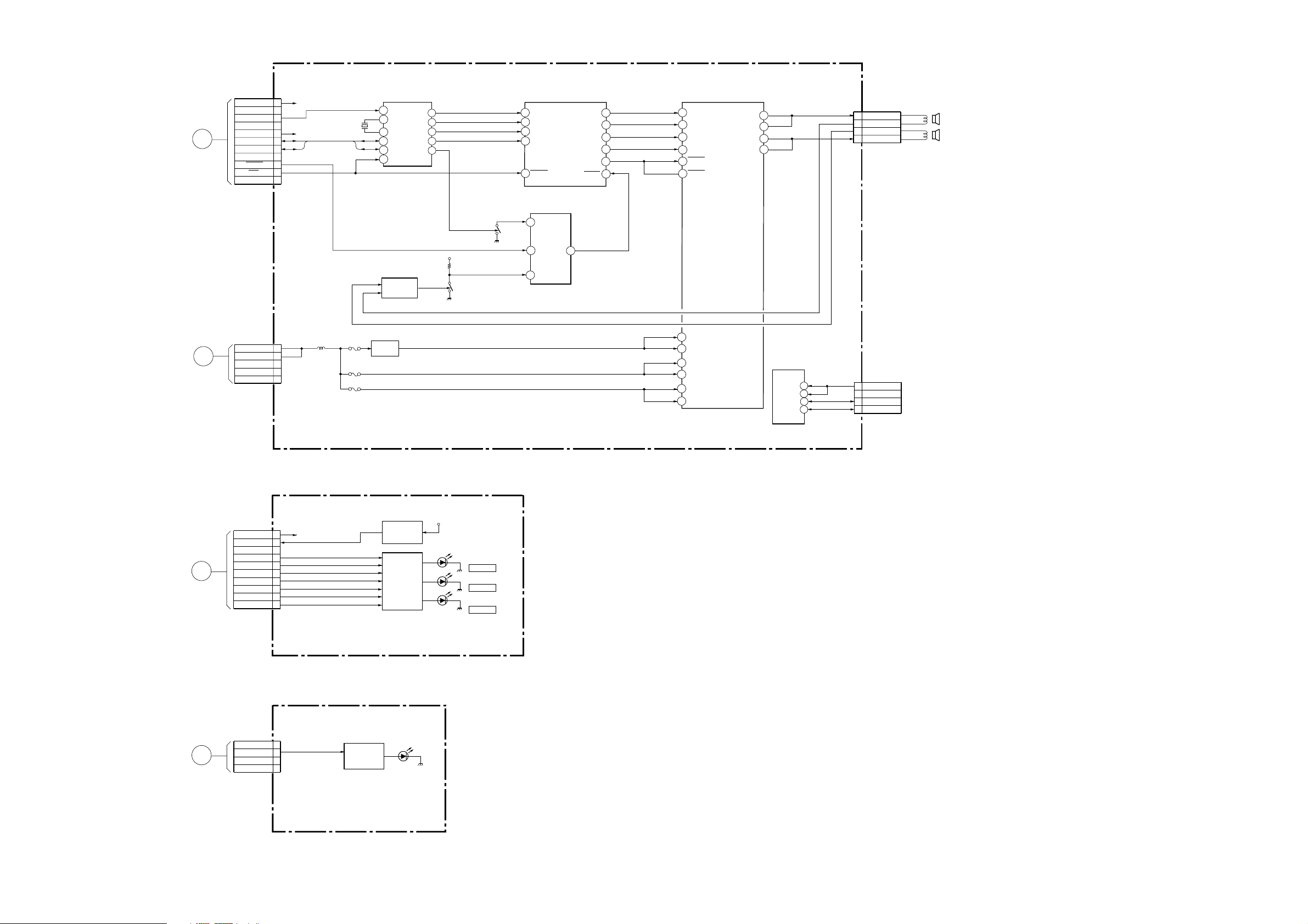
N
TO P(2/2) BOARD
CN3201
L
TO G BOARD
CN6302
CN3001
+3.3V
GND
SPDIF
GND
+12V
SDA2
SCL2
GND
MUTE
RES
GND
CN3003
AUDIO_VCC
AUDIO_VCC
GND
GND
GND
1
17
19
18
7
MCLK_IN
SCLK
SDIN
LRCLK
RESET
IC3002
PWM-AP_L
PWM-AM_L
PWM-AP_R
PWM-AM_R
VALID_L
MUTE
35
34
29
28
23
38
IC3001
1
3.3V
2
3
4
5
12V
6
7
8
9
10
11
X3001
24.576 MHz
S/PDIF RECEIVER
RX1
44
29
XTO
XTI
30
SDA
33
34
SCL
31
PDN
MCKO2
BICK
SDTO
LRCK
INT1
27
26
25
24
37
PWM DIGITAL AUDIO PROCESSOR
1
PWM-AP
PWM-AM
2
16
PWM-BP
PWM-BM
15
PWDN
13
14
RESET
IC3003
AUDIO AMP
OUTPVTA
OUTPVTA
OUTPVTB
OUTPVTB
CN3002
26
27
22
23
L+
1
L–
2
R–
3
R+
4
SPEAKER
L
R
IC3004
AND
Q3001
SW
3.3V
Q3003
Q3004-3007
1
2
3
4
5
L3006
F3003
F3001
F3002
Q3002
VCC REG.
SW
NF
5
2B
2
2Y
1B
1
1A
6
PVDDA2
32
PVDDB2
17
28
29
20
21
PVDDA1
PVDDA1
PVDDB1
PVDDB1
IC3201
AND
7
1B
8
1B
1
1B
2
1B
CN3201
3.3V
1
GND
2
SDA B
3
SCL B
4
O
TO P(2/2) BOARD
CN3202
P
TO P(2/2) BOARD
CN3204
CN701
STBY5V
SIRCS
GND
MUTE
TIMER 2
TIMER 1
POWER
STBY
SAVING 9
GND
CN751
STBY5V
LOGO
NC
GND
( AUDIO OUT )
K
1
STBY 5V
2
3
4
5
6
7
8
10
(SIRCS, LED)
R1
1
2
3
4
Q751-754
LED SW
IC701
SIRCS
OUT
Q701-706
LED SW
D751
|
D754
VCC
STBY 5V
D701
POWER
D703
TIMER
D705
MUTE
R2
(LED)
KLV-30MR1(AEP) 3-3
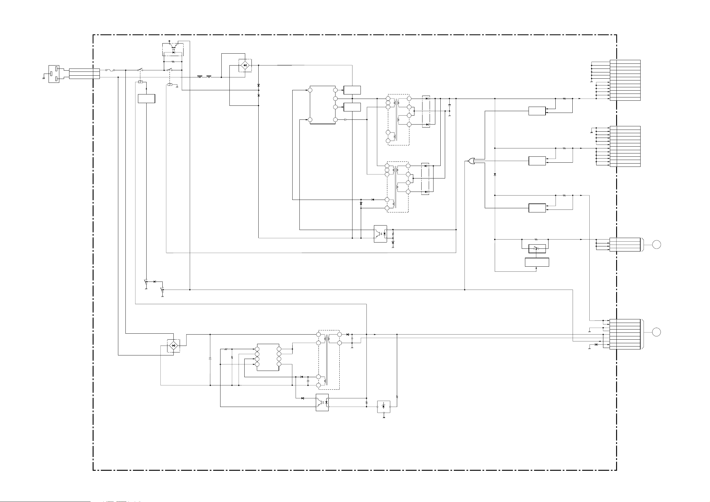
STBY 6.5V
AC INLET
CN6000
L
N
PH6001
F6000
1
2
3
RY6001
RELAY
DRIVE
Q6301
R6011
RY6000
L6001
PFC
L6000
PFC
D6000
RECT
D6002
RECT
D6001
RECT
VC18
F/B2
IC6000
DRIVER
VS 15
VD 12
OCP 9
CN6300
1
GND
GND
2
GND
3
GND
4
GND
5
GND
6
24V
7
8
Q6000
16VG
SW
Q6001
SW
D6008
T6301
PIT
1
2
3
4
5
T6302
PIT
1
2
3
4
5
D6300
9
8
7
6
D6307
D6308
D6301
9
8
7
6
D6310
D6312
Q6305
24V
DET
Q6306
24V
DET
Q6308
CURRENT
DET
R6332 24V
R6336 24V
R6340 24V
24V
9
24V
10
24V
11
24V
12
24V
CN6301
1
GND
GND
2
GND
3
GND
4
GND
5
GND
6
24V
7
8
24V
9
24V
10
24V
11
24V
12
24V
TO LCD
UNIT BOARD
TO LCD
UNIT BOARD
Q6300
SW
Q6302
SW
D6009
1
2
3
4
IC6001
DRIVER
PH6000
4
1
3
2
IC603
VREF
T6300
1
2
8
7
6
5
D6012
D6019
4
3
3
4
PH6300
SRT
D6306
RECT
8
7
1
2
STBY 6.5V
IC6301
VREF
3
1
2
R6327
Q6304
SWITCH
DRIVE
Q6303
ACTIVE FILTER
24V
TH6300
1
2
3
4
1
2
3
4
5
6
7
8
9
CN6302
24V
24V
GND
GND
CN6303
24V
24V
GND
GND
STBY6.5V
STBYGND
POWER ON
THERMO G
STBYGND
L
TO K BOARD
CN3003
M
TO P(2/2)BOARD
CN8001
G(POWER)
KLV-30MR1(AEP) 3-4
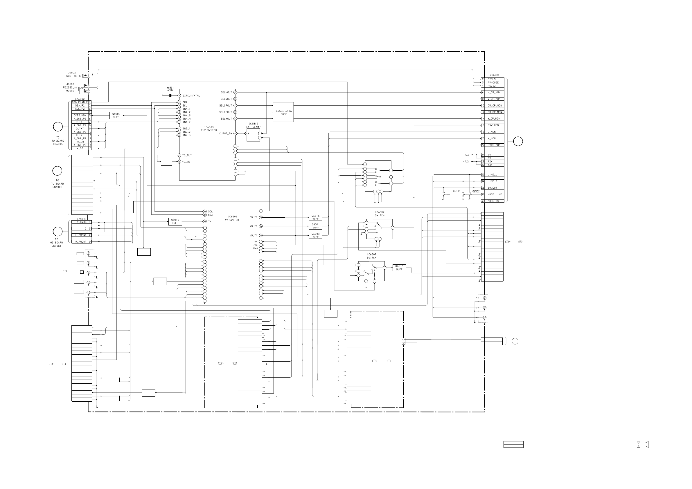
3-1-2. MEDIA RECEIVER UNIT (MBT-MRL1)
W
CN6503
1
U
C
DVD IN
S
3/
(SMART LINK)
CVBS_TUN
GND_TUN
L_TVAU
AV_AGND
R_TVAU
AV_AGND
L_AVSW
AV_AGND
R_AVSW
FSW_SEL0
FSW_SEL1
FSW_AUTO
AVLINK_SC3
AVLINK_SC4
SC2_V MUT
P /C
RR
P /C
BB
Y
L/G/S/I
R/D/D/D
J6505
SCART3
R OUT
R IN
L OUT
GND
GND
L IN
NC
MODE
GND
AVL
NC
NC
GND_C IN
NC
C IN
NC
GND_V OUT
GND_Y/V IN
V OUT
Y/V IN
GND
10
11
12
13
14
15
10
11
12
13
14
15
16
17
18
19
20
21
2
3
4
5
6
7
8
9
J6504
1
2
3
4
5
6
7
8
9
LV1
C2-1
C1N1
Y1N3
V
C
Y
Q
6517
BUFF
C1N1
RV1
V1
Q
BUFF
6510
Q
6517
BUFF
Q
BUFF
6516
V
Y
1819RV3
C
LTV
62
64
RTV
5254LOUT1
ROUT1
V3
15
16
LV3
17
Y3
C3
S2-1
6
5
C1
3
Y1
LV1
2
4
RV1
V1
1
C1N1
51
LOUT2
43
45
ROUT2
V2
8
9
LV2
11
RV2
44
VOUT3
IN3-1
IN3-2
IN3-3
IN1-1
IN1-2
IN1-3
IN3-H
IN1-H/L1
J6506
SCART1
1/
1
2
3
33
34
35
4
36
S2-4
S2-2
LV6
RV6
S2-3
LV5
RV5
LOUT3
ROUT3
VOUT4
R OUT
R IN
L OUT
GND
GND_B
L IN
BLUE
MODE
GND_G
NC
GREEN
NC
GND_R
GND_FBLK
RED
BLK
GND_V OUT
GND_V IN
V OUT
V IN
GND
2
R
B
G
R
B
G
G
B
R
36DC OUT
BLK1
BLK2
22
23
25
27
13
59
V6
60
61
20
29
30
V5
31
38
40
44
Q
6508
BUFF
1
2
3
4
5
6
7
8
9
10
11
12
13
14
15
16
17
18
19
20
21
B
G
R
B
G
R
BLK1
BLK2
NC
NC
1
2
3
4
5
6
7
8
9
10
11
12
13
14
15
16
17
18
19
20
21
R OUT
R IN
L OUT
GND
GND_B
L IN
BLUE
MODE
GND_G
AV_LINK
GREEN
NC
GND_R
GND_FBLK
RED
BLK
GND_V OUT
GND_V IN
V OUT
V IN
GND
G
B
R
SEL0
5
1
3
EN
12
1
2
3
5
12
13
0
12
1
14
2
15
3
11
2
IC6508
SWITCH
C
B
A
11
9
10
B
A
10
9
SEL0
SEL1
7
4
CENTER
SPEAKER IN
J6508
SCART4
4/
(SMART LINK)
G
15
B
4
R
14
Q6501
1
R OUT
2
R IN
3
L OUT
4
GND
5
13
TB6501
2
+
1
-
B
G
R
6
7
8
9
10
11
12
13
14
15
16
17
18
19
20
21
1
2
CENTER+
CENTER-
GND_B
L IN
BLUE
MODE
GND_G
NC
GREEN
NC
GND_R
GND_FBLK
RED
BLK
GND_V OUT
GND_V IN
V OUT
V IN
GND
J6509
W/G/W/G
L/G/S/I
R/B/D/D
CN6504
U
( AC SWITCH,
INPUT TERMINAL )
Y
TO
A(1/4) BOARD
CN4001
J6509
SCART2
2/
T
TU BOARD
CN6002
TO
CN6504
CENTER+
CENTER-
1
2
TB6501
2
1
+
-
SPEAKER IN
CENTER
KLV-30MR1(AEP) 3-5
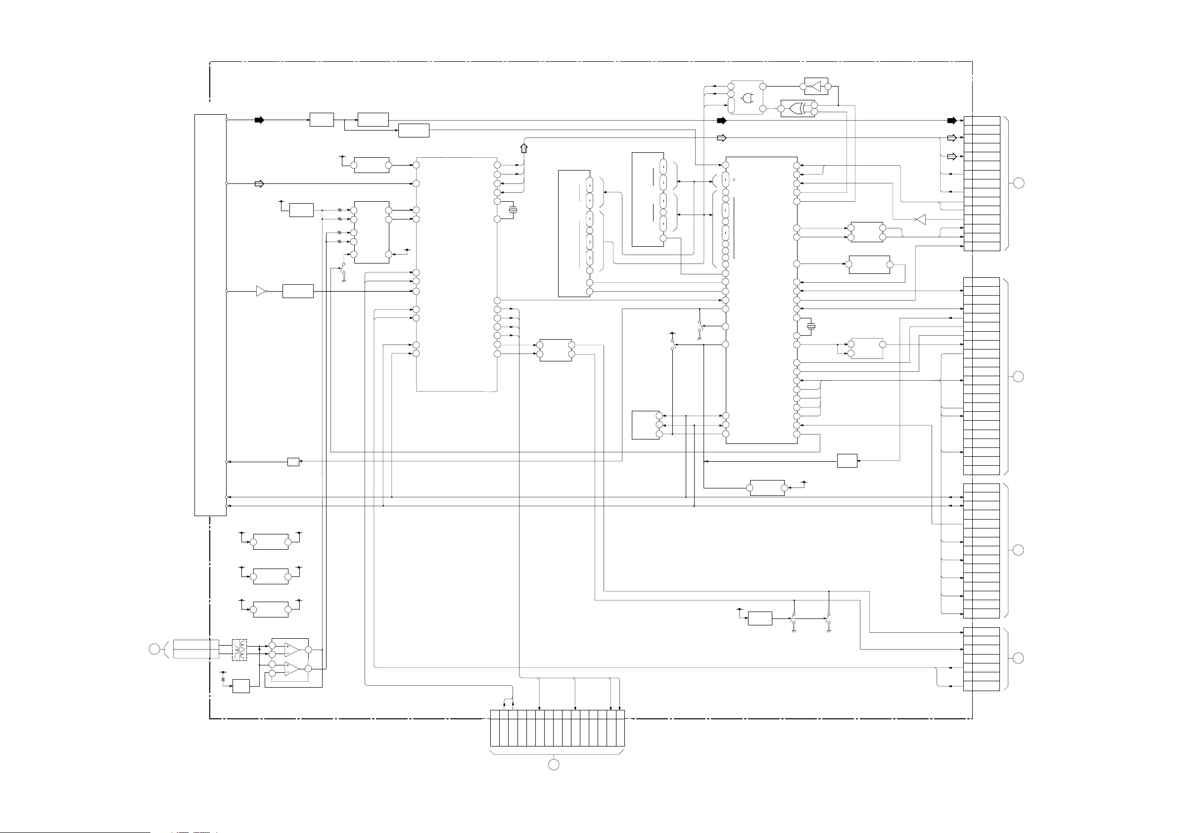
T
TO
U BOARD
CN6504
CN6002
CEN TER(+)
CEN TER(–)
TU6001
TUNER
VIDEO
FM/AM
QSS
AGC
SDA
SCL
A12V 33V
A12V A9V
A6V A5V
T6001
TRANSFORMER
1
2
+
9V
Q6001
BIAS
VIDEO
AUDIO
Q6003
6
VIN
I
VCC
IC6008
33V REG
IC6002
9V REG
IC6001
5V REG
AUDIO–BUFF
5
6
3
2
9V
SW
O
OUT
Q6004, 6005
BUFF
FL
16
16
1
IC6003
Q6002
5V REG
IC6019
NAND
A12V
9
12244
IC6012
PAINTERII
SC2_V_MUT
CENTER_POL
IC6018
RESET
RESET VCC
Q6016
MUTE SW
FSW_SEL0
FSW_SEL1
FSW_AUTO
ROMBK_1
ROMBK_0
AVLINK3
AVLINK4
AVL_OUT
AVL_IN
XTAL OUT
XTAL IN
VSYNC
HSYNC
TXT VIDEO
Q6017
MUTE
8
11
10
•
AUDIO L/R
Q6012
VIDEO
59
85
92
51
49
40
36
33
27
26
23
15
19
10
25
22
73
83
84
98
13
COINCIDENCE
D(0)
D(7)
A(0)
8
A(17)
3
PSEN
9
RD
WR
RESET–AUDIO
AGC_MONITOR
6
AGC_DEFEAT
RESET
SCL1
SDA1
INVM_WP
Q6000
BUFF
7
1
9V
Q6010
Q6006, 6007
BUFF
IC6006
V REF
IC6004
D1/CENT SW
X–COM
2Y
Y–COM
2X
3Y
4
3X
11
31
132
315
910
Q6008, 6009
BUFF
39
60
47
48
9V
53
54
67
50
51
2
3
AHVSUP
MONO_IN
SC1_IN_L
SC1_IN_R
SC2_IN_L
SC2_IN_R
IF_IN1
SC3_IN_L
SC3_IN_R
SCL
SDA
IC6005
AV SW
POWER ON_RESET
SC1_OUT_L
SC1_OUT_R
SC1_IN_L
SC1_IN_R
XTAL_IN
XTAL_OUT
SC2_OUT_L
SC2_OUT_R
SP_OUT_L
SP_OUT_R
SC3_OUT_L
SC3_OUT_R
IC6021
AUDIO L/R
37
36
56
57
71
X6001
18,432MHz
72
21
34
33
28
27
25
24
6
RIN
7
IC6007
HP AMP
LIN
IC6020
256K SRAM
D(0)
D(7)
A(0)
A(17)
LOUT
3
ROUT
1
21
23
25
29
1
4
7
9
16
17
20
31
OE
32
WE
5
NEW OTP+ SOCKET
13
D(0)
15
17
21
D(7)
2
A(0)
12
23
25
A(17)
30
24
G
Q6013, 6014
IC6011
EEPROM
SCL
6
SDA
5
WC
7
–5V
SCLO
SDA0
BUSY
R–TXT
G–TXT
B–TXT
IC6016
VDS
INT
13
IC6017
1
2
VIDEO
AUDIO L
94
95
96
57
58
16
17
78
79
81
80
82
71
X6002
12MHz
70
52
97
29
55
53
48
47
46
32
93
3.3V
Q6018
MUTE
AV LINK SW
7
3
5
FSW BUFF
2
1
Q6015
RESET
IC6014
CTL1
OI1
CTL2
IC6015
AV LINK IC
IC6013
Q6011
6
2
1
4
AUDIO R
15
14
13
12
11
10
9
8
7
6
5
4
3
2
1
1
2
3
4
5
6
7
8
9
10
11
12
13
14
15
16
17
18
19
20
21
22
15
14
13
12
11
10
9
8
7
6
5
4
3
2
1
1
2
3
4
5
6
7
CN6001
CVBS_TUN
GND_TUN
L_TVAU
AV_AGND
R_TVAU
AV_AGND
L_AVSW
AV_AGND
R_AVSW
FSW_SEL0
FSW_SEL1
FSW_AUTO
AVLINK_SC3
AVLINK_SC4
SC2_V MUT
CN6006
5V STBY
SCL
5V STBY
SDA
RESET
INT
BUSY
YS_TEXT
H_CD
GND_TEXT
GND
B_TEXT
GND_CD
GND_TEXT
V_CD
G_TEXT
GND_CD
GND_TEXT
GND
R_TEXT
GND_CD
GND_TEXT
CN6005
RGB_EN
SDA_P2
SCL_P2
D_GND_P2
CVBS_MON
A_GND_P2
R_TXT
A_GND_P2
G_TXT
A_GND_P2
B_TXT
A_GND_P2
H_CD
A_GND_P2
V_CD
CN6003
L_HP
GND
R_HP
GND
L_PC
GND
R_PC
U
V
W
D
TO
U BOARD
CN6503
TO
A(1/4) BOARD
CN4002
TO
U BOARD
CN6502
TO
H2 BOARD
CN9054
TU(TUNER, AV SWITCH, PAINTER)
123456789
GND
R_MS
GND_FIX
L_FIX
L_MS
GND_MS
6V
GND_FIX
6V
1011121314
R_FIX
R_FIX
R_FIX
R_FIX
L_SEL
18
R-SEL
CN6004
X
TO
A(4/4) BOARD
CN5201
KLV-30MR1(AEP) 3-6
 Loading...