

Sony HCD-V919AV Service Manual

HCD-V919A V
SERVICE MANUAL
HCD-V919AV is the Amplifier, Video CD
player, Tape Deck and Tuner section in
MHC-V919AV.
This stereo system is equipped with the Dolby Btype noise reduction system and Dolby Pro Logic
Surround decoder*.
* Manufactured under license from Dolby Laboratories Licensing Corporation.
DOLBY , the doub le-D symbol a and “PR O LOGIC”
are trademarks of Dolby Laboratories Licensing Corporation.
CD
Section
Tape
Deck
Section
E Model
Chinese Model
Model Name Using Similar Mechanism HCD-V717
CD Mechanism Type CDM38L-5BD24AL
Base Unit Name BU-5BD24AL
Optical Pick-up Name KSS-213D/Q-NP
Model Name Using Similar Mechanism HCD-V717
Tape Transport Mechanism Type
TCM-230AWR1/
230PWR1
SPECIFICATIONS
– Continued on next page –
MICROFILM
MINI Hi-Fi COMPONENT SYSTEM
HCD-V919AV
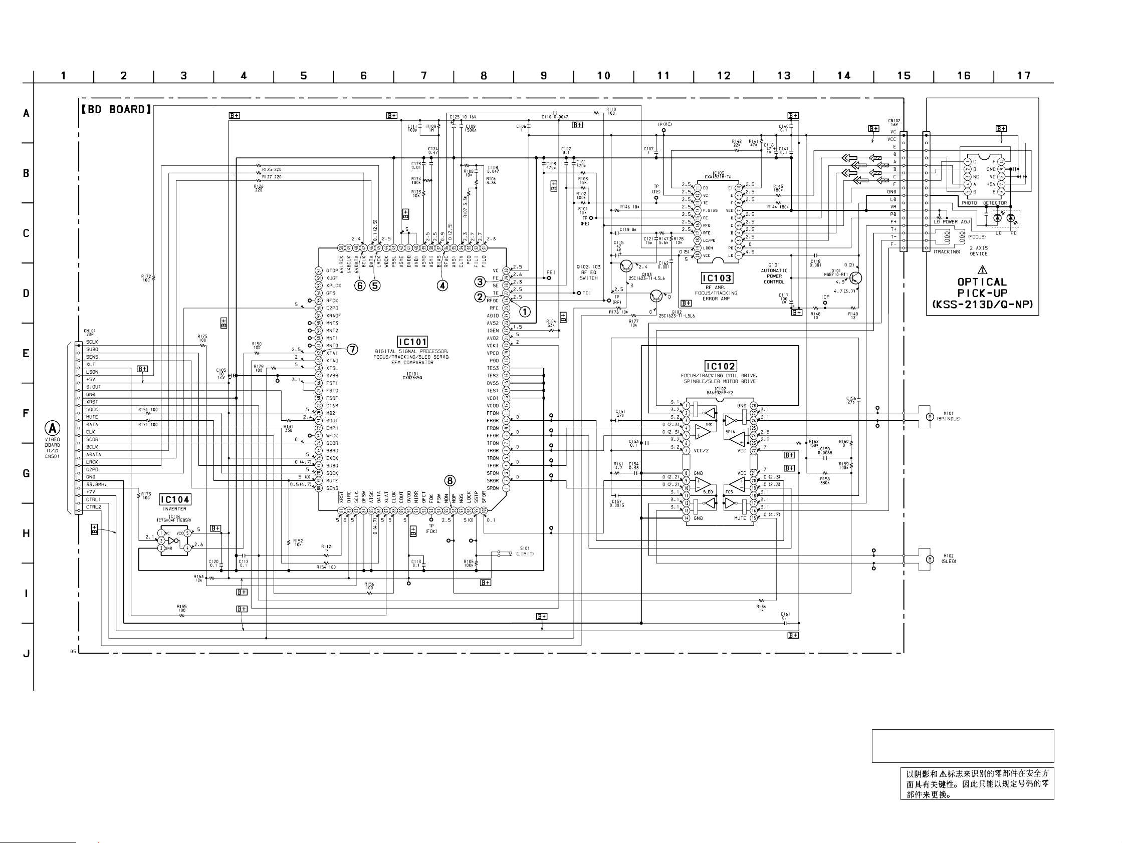
7-9. SCHEMATIC DIAGRAM – BD Section – • See page 86 for Waveforms. • See page 90 and 91 for IC Block Diagrams.
(Page 43)
The components identified by mark ! or dotted
line with mark ! are critical for safety.
Replace only with part number specified.
• Voltages and w av eforms are dc with respect to ground in
CD play mode.
no mark : CD stop
( ) : CD play
– 39 –
– 40 –
HCD-V919AV
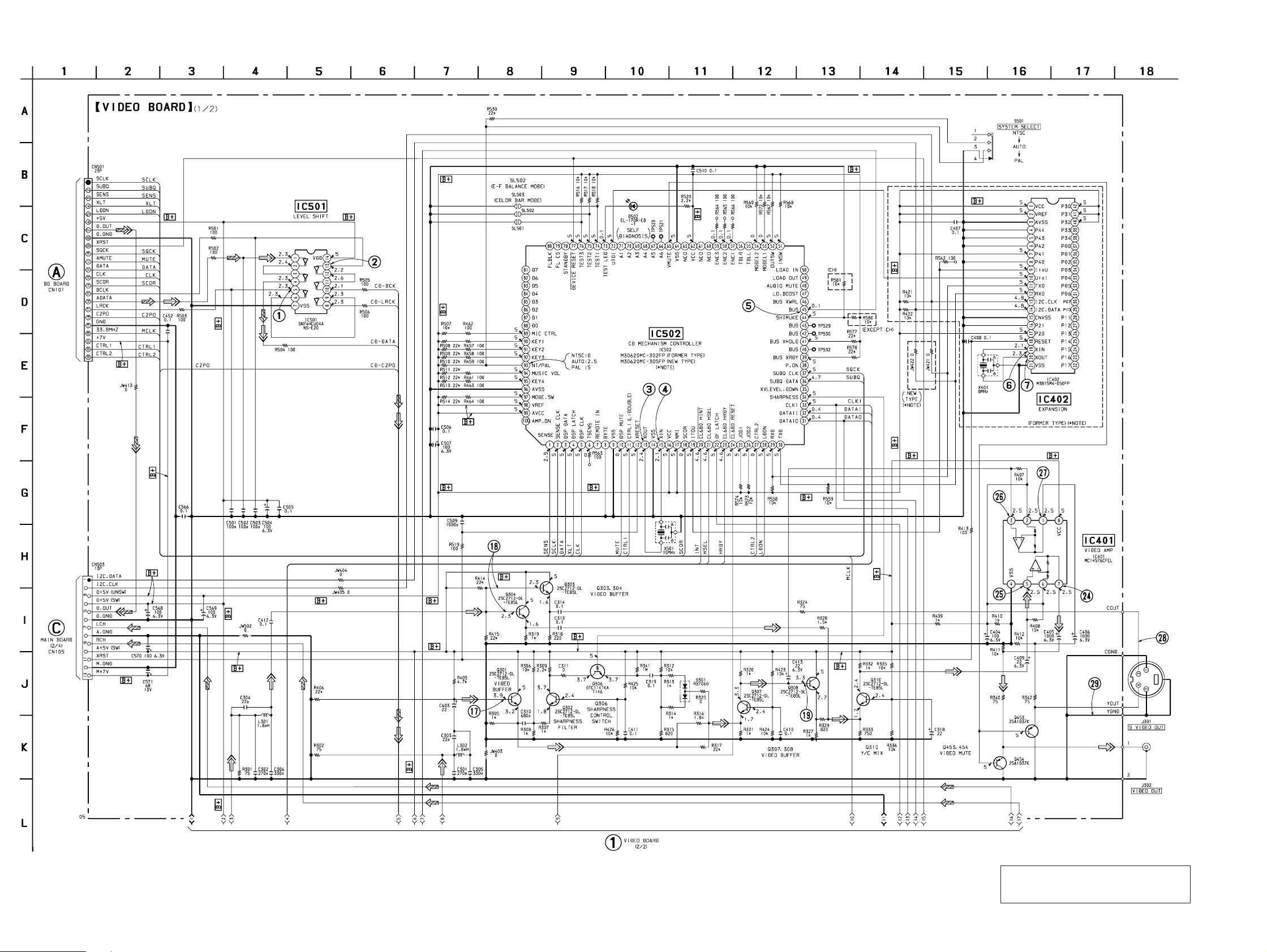
7-11. SCHEMATIC DIAGRAM – VIDEO Section (1/2) – • See page 91 for IC Block Diagram.
(Page 39)
(Page 62)
– 43 –
(Page 45)
• Voltages and w av eforms are dc with respect to ground in
VIDEO CD play mode.
no mark : VIDEO CD play
– 44 –
*Note
When replacing IC502, refer to “IC502 of
VIDEO board” in “Servicing Notes” (page 4).
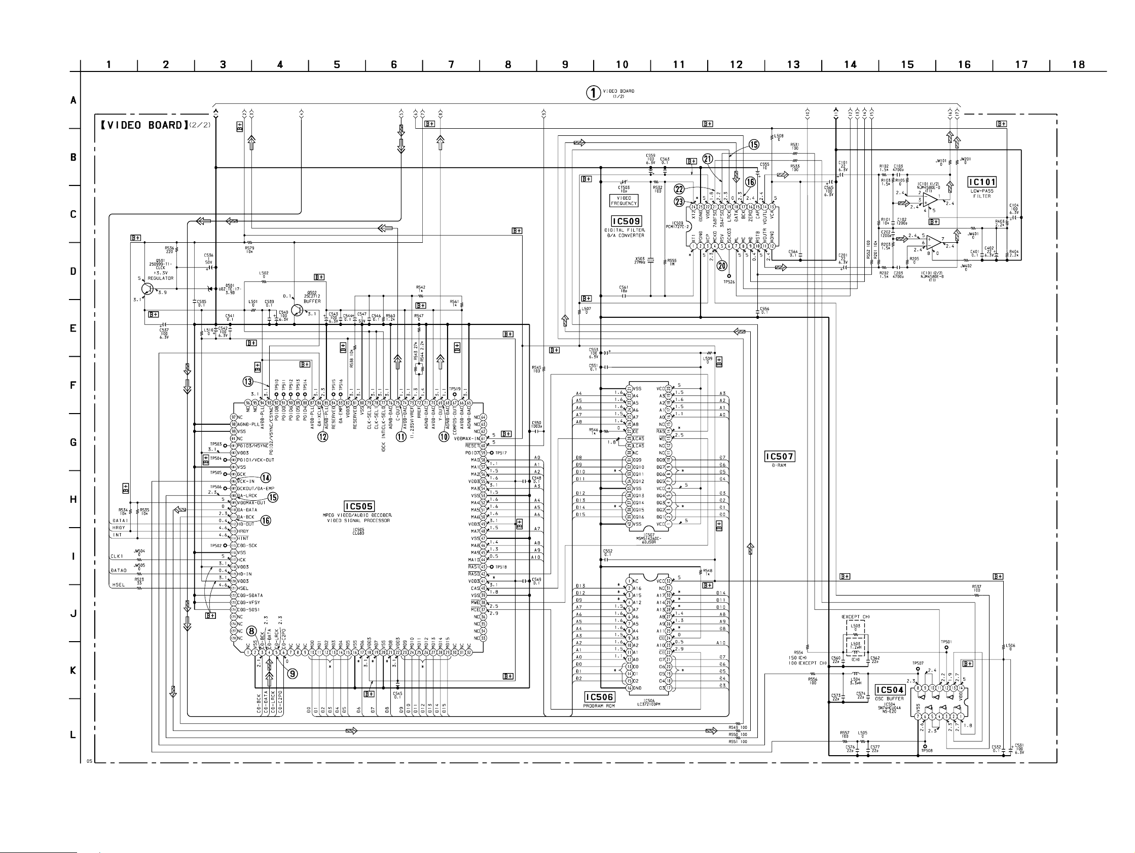
7-12. SCHEMATIC DIAGRAM – VIDEO Section (2/2) – • See page 86 to 88 for Waveforms. • See page 91 for IC Block Diagram.
(Page 43)
HCD-V919AV
– 45 –
– 46 –
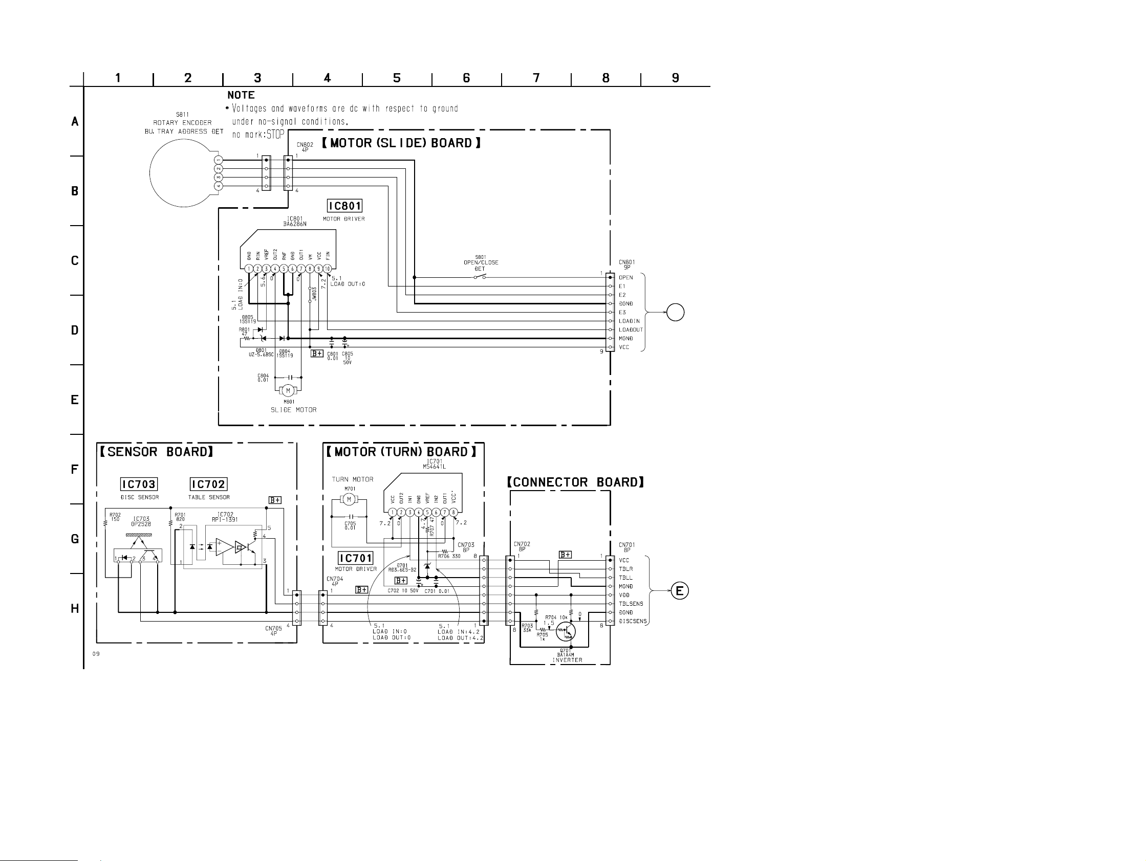
7-14. SCHEMATIC DIAGRAM – CD MOTOR Section – • See page 92 for IC Block Diagrams.
F
(Page 62)
HCD-V919AV
MAIN BOARD
CN104
– 49 –
MAIN BOARD
CN103
(Page 62)
– 50 –
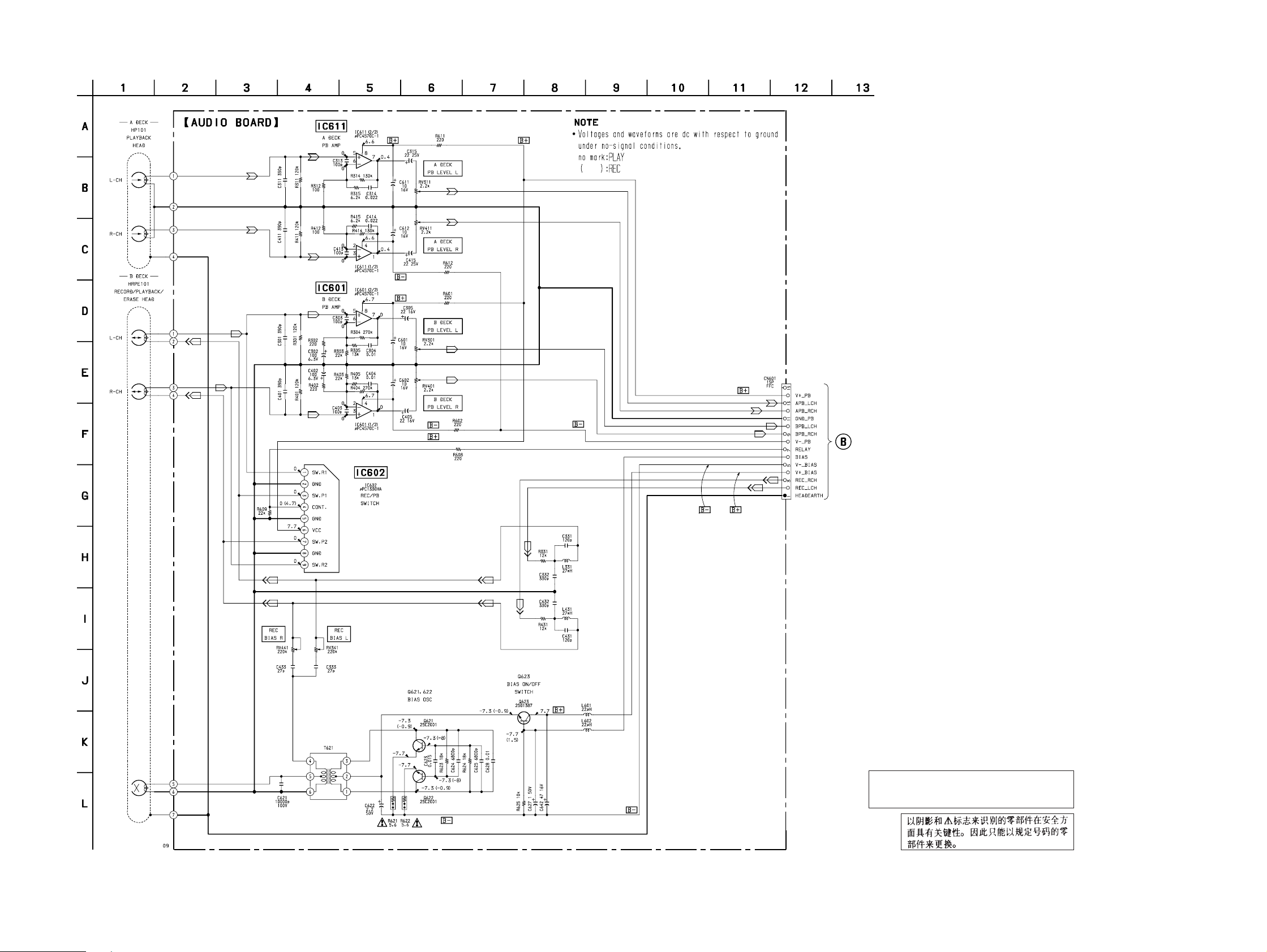
7-16. SCHEMATIC DIAGRAM – TAPE DECK Section – • See page 92 for IC Block Diagram.
HCD-V919AV
MAIN BOARD
(Page 60)
CN106
– 53 –
The components identified by mark ! or dotted
line with mark ! are critical for safety.
Replace only with part number specified.
– 54 –
HCD-V919AV
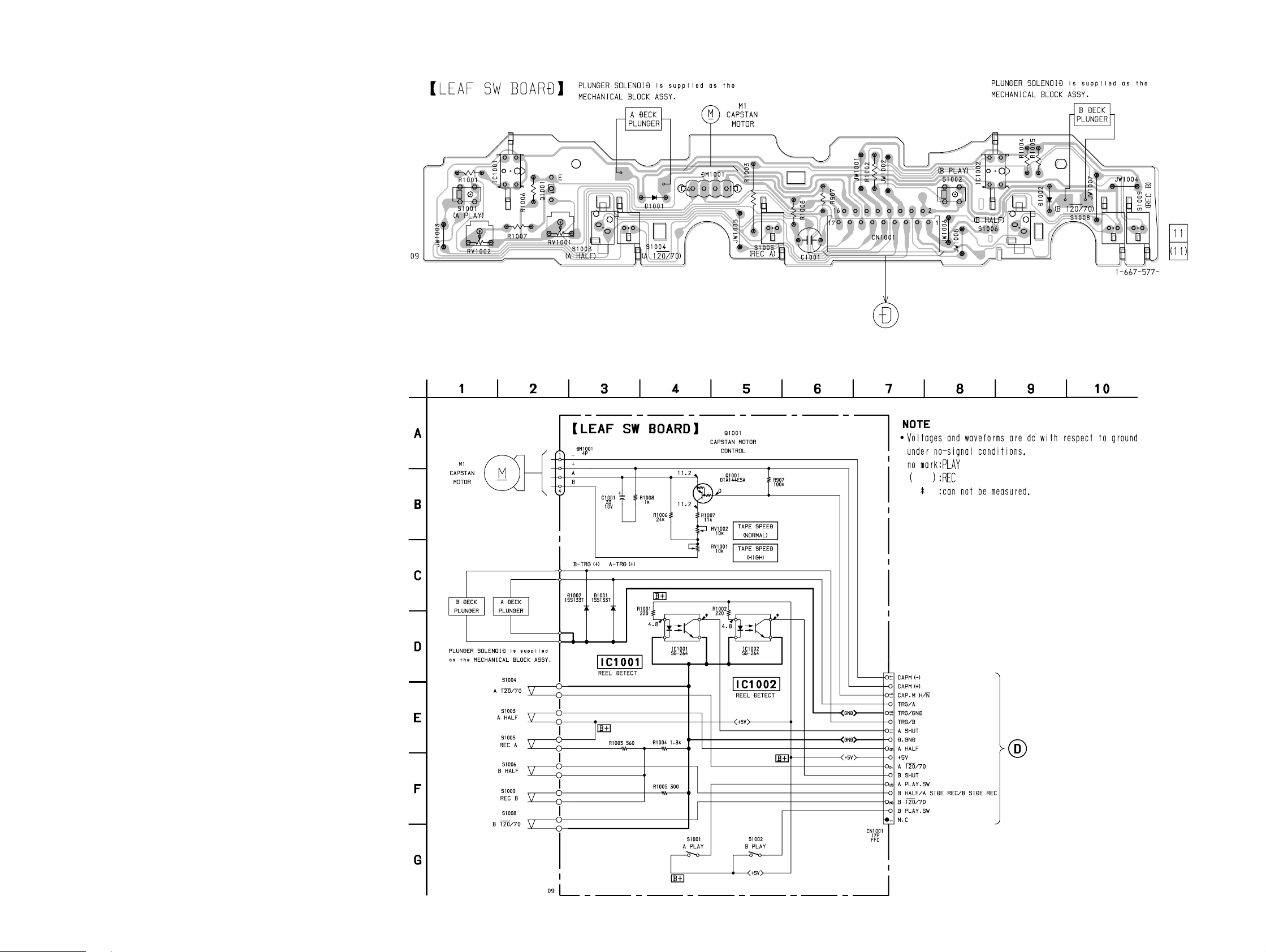
7-17. PRINTED WIRING BOARD – LEAF SW Section – • See page 35 for Circuit Boards Location.
MAIN BOARD
CN107
(Page 57)
7-18. SCHEMATIC DIAGRAM – LEAF SW Section –
– 55 –
MAIN BOARD
CN107
(Page 60)
– 56 –
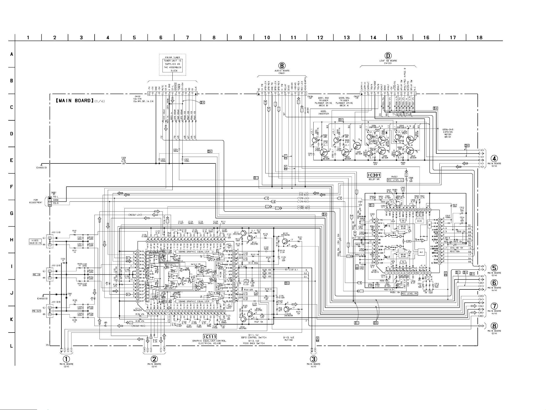
HCD-V919AV
7-20. SCHEMATIC DIAGRAM – MAIN Section (1/4) –
(Page 56)
(Page 54)
(Page 61)
(Page 61)
(Page 65)
(Page 63)
– 59 –
(Page 63)
(Page 65)
(Page 61)
(Page 65)
• Voltages and waveforms are dc with respect to ground
under no-signal (detuned) conditions.
no mark : FM
– 60 –
 Loading...