

Page 1

HCD-V5500
SERVICE MANUAL
• HCD-V5500 is the deck, CD section
in MHC-V5500/V7700AV.
Manufactured under license from Dolby Laboratories
Licensing Corporation.
“DOLBY” and the doub le-D symbol a are trademarks
of Dolby Laboratories Licensing Corporation.
CD CD Mechanism Type CDM38-5BD21
Section Base Unit Name BU-5BD21
Tape deck Model Name Using Similar Mechanism HCD-V8800
Section T ape Transport Mechanism T ype TCM-220WR2E
E Model
Chinese Model
Model Name Using Similar Mechanism HCD-V8800
Optical Pick-up Type KSS-213B/S-N
VIDEO CD/CD player section
System Compact disc and digital
audio system
Laser Semiconductor laser
(λ=780nm)
Emission duration:
continuous
Laser output Max.44.6 µW*
*This output is the value
measured at a distance of
200 mm from the
objective lens surface on
the Optical Pick-up Block
with 7 mm aperture.
Audio
Frequency response 2 Hz - 20 kHz(±0.5 dB)
Wavelength 780 - 790 nm
Signal-to-noise ratio More than 90 dB
Dynamic range More than 90 dB
Video
Color system format NTSC, PAL
SPECIFICATIONS
CD OPTICAL DIGITAL OUT
(Square optical connector jack, rear panel)
Wavelength 600 nm
Output Level –18 dBm
Tape player section
Recording system 4-track 2-channel stereo
Frequency response 60 - 13,000 Hz (±3 dB),
(DOLBY NR OFF) using
Sony TYPE I cassette
60 - 14,000 Hz (±3 dB),
using Sony TYPE II
cassette
Design and specifications are subject to change
without notice.
MICROFILM
STEREO CASSETTE DECK CD PLAYER
Page 2

TABLE OF CONTENTS
1. SERVICING NOTE
······················································ 3
2. GENERAL ······································································ 4
3. DISASSEMBLY
3-1. Back Panel, CD Block Removal········································· 5
3-2. Cassette Lid (A)/(B) Assy, Mechanism Deck Removal ···· 5
3-3. Main Board, Resistor Board, Video Board,
Video In Board, Front Panel Assy Removal ······················· 6
4. TEST MODE ·································································· 7
5. ADJUSTMENTS
5-1. Mechanical Adjustment ······················································ 8
5-2. Electrical Adjustment ························································· 8
6. DIAGRAMS
6-1. Block Diagram — CD Section — ···································· 13
6-2. Block Diagram — Video Section — ································ 15
6-3. Block Diagram — Deck/System Control Section — ······· 17
6-4. Circuit Boards Location ··················································· 19
6-5. Schematic Diagram — Audio Section —························· 20
6-6. Printed Wiring Board — Audio Section —······················ 23
6-7. Printed Wiring Board — Video Section — ······················ 26
6-8. Schematic Diagram — Video Section — ························· 29
6-9. Schematic Diagram — Main Section — ·························· 33
6-10. Printed Wiring Board — Main Section — ······················· 37
6-11. Printed Wiring Board — CD Panel Section — ················ 40
6-12. Schematic Diagram — CD Panel Section — ··················· 43
6-13. Printed Wiring Board — BD Section — ·························· 45
6-14. Schematic Diagram — BD Section — ····························· 47
6-15. Schematic Diagram — Motor Section — ························ 49
6-16. Printed Wiring Board — Motor Section —······················ 51
6-17. IC Block Diagrams ··························································· 53
6-18. IC Pin Functions ······························································· 57
7. EXPLODED VIEWS
7-1. MAIN SECTION ····························································· 69
7-2. FRONT PANEL SECTION ·············································· 70
7-3. CD MECHANISM DECK SECTION
(CDM38-5BD21) ····························································· 71
7-4. CD MECHANISM DECK SECTION-2
(CDM38-5BD21) ····························································· 72
7-5. BASE UNIT SECTION (BU-5BD21) ····························· 73
7-6. TAPE MECHANISM DECK SECTION-1
(TCM-220WR2E) ···························································· 74
7-7. TAPE MECHANISM DECK SECTION-2
(TCM-220WR2E) ···························································· 75
8. ELECTRICAL PARTS LIST ··································· 76
— 2 —
Page 3

SECTION 1
H
VIDEO board
TP709 (LED)
Oscilloscope
+
_
SERVICING NOTE
SELF-DIAGNOSIS
This model has the self-diagnosis function for the VIDEO and
AUDIO decoder sections.
Immediately after the power on, the self-diagnosis function searches
each operation of IC’s around the mechanism control microcomputer
(IC701).
The results can be checked by connecting an oscilloscope to TP709
(LED) of the VIDEO board.
Oscilloscope (Waveform) Symptom
H
No error
L
Light
Note: The LED for check (D701) is mounted to some sets
(FORMER TYPE). In this case, confirm the lighting
condition of LED.
[VIDEO BOARD] (SIDE A)
1 time blinking
2 time blinking
3 time blinking
H
External SRAM (IC751)
L
error
H
MPEG decoder (IC201)
L
error
DRAM (IC251)
error
L
D701
IC771
[VIDEO BOARD] (SIDE B)
TP709 (LED)
IC751
X901
IC251
— 3 —
Page 4

SECTION 2
GENERAL
@ª
@•
@¶
3
12 5 7 8 9 !¡
@§
4
@∞
6
@¢
@£
@™
@¡
@º
!º
!ª
!¶
!•
!™
!£
!¢
!∞
!§
1 DISC SKIP EX-CHANGE Button
(CD)
2 0 Button (CD)
3 PREV Button (CD)
4 NEXT Button (CD)
5 ) Button (CD)
6 RETURN Button (CD)
7 DISC 1 Button (CD)
8 DISC 2 Button (CD)
9 DISC 3 Button (CD)
!º SELECT Button (CD)
#º
!¡ 6 OPEN/CLOSE Button (CD)
!™ ·P CD NON-STOP Button (CD)
!£ p Button (CD)
!¢ · Button [B] (DECK)
!∞ ª Button [B] (DECK)
!§ π Button [B] (DECK)
!¶ ) Button [B] (DECK)
!• 0 Button [B] (DECK)
!ª DIRECTION MODE Button
(DECK)
@º PAUSE Button (DECK)
@¡ REC Button (DECK)
@™ HI-SPEED DUBBING Button
(DECK)
@£ CD SYNCHRO Button (DECK)
@¢ DOLBY NR Button (DECK)
@∞ ) Button [A] (DECK)
@§ 0 Button [A] (DECK)
@¶ π Button [A] (DECK)
@• ª Button [A] (DECK)
@ª · Button [A] (DECK)
#¡
#º OPTICAL DIGITAL OUT
#¡ SYSTEM CONTROL CONNECTOR
#™ SYSTEM SELECT SWITCH
#™ #£
#¢ #∞
#£ VIDEO IN JACK
#¢ MONITOR OUT JACK
#∞ S VIDEO JACK
— 4 —
Page 5

SECTION 3
0
DISASSEMBLY
Note : Follow the disassembly procedure in the numerical order given.
3-1. BACK PANEL, CD BLOCK REMOVAL
9
CD block
8
Screw
+BVTP 3
×
10
CASE
Unscrew the fi ve case attachment in the screws (case)
(M3 × 8) × 4, (+BV 3 × 8) × 1 and remove the case.
3
Back panel
1
Screw
+BVTP 3
2
Screw
+BVTP 3
×
1
×
8
7
Screw
+BVTP 3
3-2. CASSETTE LID (A)/(B) ASSY, MECHANISM DECK REMOVAL
1
Press the EJECT button and open the cassette lid.
Mechanism Deck (TCM-220WR2E)
7
+BVTP 2.6
6
Screw
4
5
CN112 (9 pin)
CN111 (8 pin)
×
10
×
8
1
Screw
+BVTP 3
Flat wire (19 core)
2
×
10
1
3
1
8
6
Screw
+BVTT 3
— 5 —
4
Flat wire (11 core)
5
Flat wire (21 core)
×
8
Page 6

3-3. MAIN BOARD, RESISTOR BOARD, VIDEO BOARD, VIDEO IN BOARD ,
d
FRONT PANEL ASSY REMOVAL
6
3
Screw
+BVTP 3
7
Bracket V (T)
9
VIDEO board
7
Bracket V (B)
×
10
Screw
+BVTP 3
×
10
8
Screw
+BVTP 3
5
!£
+BVTP 3
×
8
!º
Screw
+BVTP 3
Screw
4
×
8
×
8
!¡
VIDEO IN board
!™
Bracket (BP)
!¢
Bracket (H/S)
!∞
Resistor board
1
2
Front panel assy
Screw
+BVTP 3
×
8
• Tray (Slide) getting out procedure on the power supply is OFF
Rotate the BU CAM assembly in the direction of the arrow and pull out the slide.
!§
Screw
+BVTP 3
!¶
Main boar
×
8
Tray (Slide)
1
BU CAM assy
— 6 —
Page 7

SECTION 4
TEST MODE
VIDEO CD COLOR-BARS MODE
On this mode, the data of the color-bars signal as a picture signal
and the 1kHz sine wave signal as a sound signal are output by the
mechanism control microcomputer (IC701) for video CD signal
check. When measurement of the voltage and waveform on the
VIDEO board, perform it in this mode.
For reference, the color-bars signal can be observed at J9001
(VIDEO OUT) and the sound signal can be observed at J101
(VIDEO (AUDIO) OUT) using an oscilloscope.
1. Connect the lead wire to both ends of the land of SL701 (CAL
BAR) of the VIDEO board.
2. Turn the power on. Press FUNCTION button to select CD.
3. After 2 or 3 seconds later, connect the lead wire.
4. After measuring, remove the lead wire connected.
Note : The 1kHz sine wave is not outputted when the CD is played
once, but it is not error.
[VIDEO BARD ] (SIDE B)
SL703 (AFADJ)
SL702 (ADJ)
IC751
IC251
SL701 (CAL BAR)
— 7 —
Page 8

SECTION 5
ADJUSTMENTS
5-1. MECHANICAL ADJUSTMENT
PRECAUTION
1. Clean the following parts with a denatured-alcohol-moistened
swab:
record/playback head pinch roller
erase head rubber belts
capstan idlers
2. Demagnetize the record/playback head with a head
demagnetizer.
3. Do not use a magnetized screwdriver for the adjustments.
4. After the adjustments, apply suitable locking compound to the
parts adjusted.
5. The adjustments should be performed with the rated power
supply voltage unless otherwise noted.
• T orque Measurement
Mode Torque Meter Meter Reading
Forward CQ-102C
Forward
Back Tension (0.028 – 0.083 oz•inch)
Reverse CQ-102RC
Reverse
Back Tension (0.028 – 0.083 oz•inch)
FF, REW CQ-201B
CQ-102C
CQ-102RC
36 to 61g•cm
(0.50 – 0.84 oz•inch)
2 to 6g•cm
36 to 61g•cm
(0.50 – 0.84 oz•inch)
2 to 6g•cm
61 to 143g•cm
(0.85 – 1.99 oz•inch)
5-2. ELECTRICAL ADJUSTMENT
DECK SECTION
1. The adjustment should be performed in the publication.
(Be sure to make playback adjustment at first.)
2. The adjustment and measurement should be performed for both
L-CH and R-CH.
• Switch position
DOLBY NR switch : OFF
FUNCTION button : OFF
EFFECT switch : OFF
DBFB switch : OFF
3. Deck section electrical adjustments are made in test mode by
press key switch same time CD STOP DECK A ST OP and
DECK B STOP button.
4. Input point and output level measurement point.
• T ape Tension Measurement
Mode Tension Meter Meter Reading
Forward CQ-403A
Reverse CQ-403R
more than 100 g (3.53 oz)
more than 100 g (3.53 oz)
• Test Tape
Tape Signal Used for
P-4-A100 10 kHz, –10 dB
P-4-L300 315 Hz, 0dB Level Adjustment
WS-48B 3 kHz, 0dB Tape Speed Adjustment
0 dB=0.775V
Record/Playback Head Azimuth Adjustment
DECK A DECK B
Procedure:
1. Forward Playback mode
Reverse Playback mode
Head Azimuth Adjustment
— 8 —
Page 9

2. Turn the adjustment screw for the maximum output levels. If
t
these levels do not match, turn the adjustment screw until both
of output levels match together within 1 dB.
3. Playback Mode
Tape Speed Adjustment DECK A DECK B
Note: Start the T ape Speed adjustment as belo w after setting to the
test mode.
Set to test mode. (Press key switch same time CD STOP
DECK A STOP and DECK B STOP button.)
Test mode off. (Power off.)
Procedure:
• Perform high speed adjustment before normal speed adjustment.
Mode: Playback
4. Change the playback mode and repeat the steps 1 to 3.
5. After the adjustment, lock the adjustment screw with suitable
locking compound.
Adjustment Location:
— Record/playback head (Deck A and B) —
Speed
*High
Normal
Deck
A
B
A
B
Adjustment
RV652
RV652
RV651
RV651
Frequency counter
5,910 to 6,090 Hz
2,910 to 3,090 Hz
* Continue to press HIGH SPEED DUBBING switch (S259) in
playback mode : High speed playback.
Frequency difference between the beginning and the end of the
tape should be within ± 3%.
Frequency difference between deck A and deck B the beginning
of the tape should be within 1.5 %.
Adjustment Location: AUDIO board (See page 10)
Sample Value of Wow and flutter
W.RMS (JIS) within 0.3%
(test tape: WS-48B)
Playback level Adjustment DECK A DECK B
Procedure:
— FWD playback Mode —
test tape
P-4-L300
(315 Hz, 0 dB)
VTVM
set
Output level measurement poin
(See page 8)
+
–
Deck A is RV311 (L-CH) and RV411 (R-CH), Deck B is RV301
(L-CH) and RV401 (R-CH) so that adjustment within adjustment
level as follows.
Adjustment Level:
LINE OUT level : –8.2 to –7.2 dB (301.5 to 338.3 mV)
Level Difference between Channels : within 0.5 dB
Confirm the OUTPUT level does not change in playback mode
while changing the mode from playback to stop several times.
Adjustment Location: AUDIO board (See page 10)
— 9 —
Page 10

Record Bias Adjustment DECK B
)
Procedure:
1. Record mode
1) 315 Hz
2) 10 kHz
AF OSC
attenuator
50.1mV (–23.8dBs)
set
blank tape
CS-123
Adjustment Level:
OUTPUT level: –23.8 dB ± 1.0 dB (56.1 to 44.6 mV)
Adjustment Location: MAIN board
Adjustment Location :
[AUDIO BOARD] — Component Side —
RV301 : Playback Level (Deck B L-CH)
RV401 : Palyback Level
(Deck B R-CH)
RV651 : Tape Speed (Normal)
Input point (See page 8)
2. Mode: Playback
3. Confirm playback the signal recorded in step 1 become
adjustment level as follows.
4. If these levels do not adjustment level, adjustment the RV341
(L-CH) and RV441 (R-CH) to repeat steps 1 and 4.
Adjustment level: Playback output of 315 Hz to playback output
of 10 kHz: 0 ± 1.0 dB (0 ± 4.5mV).
Adjustment Location: AUDIO board
Record Level Adjustment DECK B
Procedure:
1. Record mode
RV341 : Record Bias (L-CH)
RV441 : Record Bias (R-CH)
RV411 : Playback Level (Deck A R-CH)
[MAIN BOARD] — Component Side —
RV451 Record Level (R
CNB108
RV401 Record Level (L)
RV652 : Tape Speed
(Hight)
RV311 : Playback Level
(Deck A L-CH)
2. Playback mode
3. Confirm playback the signal recorded in step 1 become
adjustment level as follows.
4. If these levels do not adjustment level, adjustment the RV401
(L-CH) and RV451 (R-CH) to repeat steps 1 and 4.
— 10 —
Page 11

CD SECTION
BD board
Oscilloscope
TP (RF)
TP (VC)
Note :
1. CD Block is basically designed to operate without adjustment.
Therefore, check each item in order given.
2. Use YEDS-18 disc (3-702-101-01) unless otherwise indicated.
3. Use an oscilloscope with more than 10MΩ impedance.
4. Clean the object lens by an applicator with neutral detergent
when the signal level is low than specified value with the
following checks.
S Curve Check
Oscilloscope
BD board
TP (FE)
TP (VC)
RF Level Check
Procedure :
1. Connect oscilloscope to test point TP (RF) on BD board.
2. Turned Power switch on.
3. Put disc (YEDS-18) in to play the number five track.
4. Confirm that oscilloscope waveform is clear and check RF
signal level is correct or not.
Note : A clear RF signal waveform means that the shape “◊” can
be clearly distinguished at the center of the waveform.
RF signal waveform
Procedure :
1. Connect oscilloscope to test point TP (FE) on BD board.
2. Connect between test point TP (FEI) and TP (VC) by lead wire.
3. Turned Power switch on.
4. Put disc (YEDS-18) in and turned Power switch on again and
actuate the focus search. (actuate the focus search when disc
table is moving in and out.)
5. Check the oscilloscope waveform (S-curve) is symmetrical
between A and B. And confirm peak to peak level within 3 ± 1
Vp-p.
S-curve waveform
Symmetry
A
Within 3
B
±
1 Vp-p
6. After check, remove the lead wire connected in step 2.
Note : • Try to measure several times to make sure than the ratio
of A : B or B : A is more than 10 : 7.
• Take sweep time as long as possible and light up the
brightness to obtain best waveform.
VOLT/DIV : 200mV
TIME/DIV : 500ns
Level : 1.3 Vp-p
+0.25
–0.20
— 11 —
Page 12

RF PLL Free-run Frequency Check
r
r
Procedure :
1. Connect frequency counter to TP (PLCK) with lead wire.
VIDEO SECTION
Frequency adjustment
BD baord
TP (PLCK)
frequency counte
2. Turned Power switch on.
3. Put the disc (YEDS-18) in to play the number five track.Conf irm
that reading on frequency counter is 4.3218 MHz.
Adjustment Location :
[BD BOARD] — SIDE A —
(FEI)
(FE)
(TE)
(PLCK)
IC103
(RF)
(VC)
1. Connect the frequency counter to check point of the VIDEO
board.
frequency counte
VIDEO board
TP410 (DCLK)
2. Adjust CT401 of the VIDEO board so that the frequency counter
read 13.5 MHz ± 40 Hz at STOP condition.
[VIDEO BOARD] — SIDE B —
SL703 (AFADJ)
SL702 (ADJ)
IC751
IC251
SL701 (CAL BAR)
CT401
Frequency
TP410 (DCLK)
IC101
— 12 —
Page 13

6-1. BLOCK DIAGRAM — CD SECTION —
HCD-V5500
SECTION 6
DIAGRAMS
OPTICAL PICK-UP
BLOCK (KSS-213B/S-N)
LASER
DIODE
POWER
PD
LD
DETECTOR
E
AC
BD
F
TRACKING
COIL
FOCUS
COIL
IC107
RF AMP
APC LD
2
AMP
1
3
4
SUMMING
5
6
TRACKING
8
9
FOCUS/TRACKING COIL DRIVE
SPINDLE/SLED MOTOR DRIVE
1
2
16
17
13
12
27
26
AMP
ERROR
AMP
IC103
RF
FOCUS
ERROR
BUFFER
19
RF
RF FQ
16
AMP
AMP
VC
IC102
15
13
1110
VC
12
4
5
19
20
10
9
23
24
INTEGRATOR
INTE-
GRATOR
LD
LD
DRIVE
Q101
4
1
VC
T+
T–
F+
F–
M102
SLED
M
MOTOR
M101
SPINDLE
M
MOTOR
DIGITAL SERVO
DIGITAL SIGNAL PROCESSOR
IC101
ASY0
39
RF AC
36
ASY1
ASYMMETRY
38
CORRECTION
RF DC
26
TE
27
28
29
4
6
8
10
2
100
96
SE
FE
TFDR
TRDR
FFDR
FRDR
SRDR
SFDR
MDP
A/D
CONVERTER
MIRR
DFCT
FOK
DETECTOR
62
XTAL
CLOCK
GENERATOR
DIGITAL
PLL
EFM
DEMODULATOR
SYNC
PROTECTOR
TIMING
GENERATOR 1
CLV SERVO
PROCESSOR
1B TIMS
OVERSAMPLING
FILTER
NOISE
SHAPER
REGISTER
CORRECTOR
GENERATOR 2
MIX
FOK
DFCT
MIRR
SERVO DSP
FOCUS
SERVO
TRACKING
SERVO
SLED
SERVO
PWM
GENERATOR
TRACKING
PWM
GENERATOR
FOCUS
PWM
GENERATOR
SLED
PWM
GENERATOR
ERROR
TIMING
DATA BUS
PRIORITY
EMCODER
ADDRESS
GENERATOR
32K
RAM
D/A
DATA
PROCESSOR
79 54
MUTE
+5V
MD2
70
DOUT
DIGITAL
OUT
PEAK
DETECTOR
SERIAL/PARALLEL
PROCESSOR
GFS
S STOP
99
+5V
SERVO
INTERFACE
S101
LIMIT
SWITCH
SUBCODE
P-W
PROCESSOR
SUBCODE
Q
PROCESSOR
INTERFACE
SEQUENCER
CPU
SERVO
AUTO
EXCK
SBSO
SUBQ
SQCK
SCLK
DATA
LRCK
BCLK
SCOR
WFCK
DATA
SENS
C2PO
DFCT
MIRR
XRST
71
76
75
77
78
83
46
45
47
74
73
86
XLT
87
CLK
88
80
56
FOK
93
92
91
81
DIGITAL
OUT
OPTICAL
1
LDON
384BD
EXCK
SUBQ
SUBQ
SQCK
SCLK
ADATA
LRCK
BCLK
SCOR
B
DATA
VIDEO
XLT
SECTION
CLK
(Page 15 )
SENS
C2PO
XRST
AMUTE
16
15MUTE
• SIGNAL PATH
: CD
: DIGITAL OUT
: VIDEO
— 13 — — 14 —
Page 14

HCD-V5500
6-2. BLOCK DIAGRAM — VIDEO SECTION —
BUFFER
X202
X201
9
8
7
6
5
IC501 (1/2)
XTL0O
2
XTL01
3
106
XTL2O
107
XTL2I
73
DATA
78
CLK
74
AMUTE
11
SQCK
10
SUBQ
77
SCLK
XLT
76
75
LDON
71
SCOR
62
SENS
RESET
48
112
11
111
12
110
13
109
14
103
15
100
101
102
D-RAM INTERFACE
38–43 46–55•
2–5 7–10 35–38 40–43
•
•
•
DQ1
A0
I/O8
I/O1
2–10 21 23–25
•11–13 15–19
21–29 • 31–3513 – 20
D7
D0
CD-ROM
DECODER
MPEG
AUDIO
DECODER
17–21 23 24 32 33••••
18–21 24–28•
A0
DQ16
D-RAM
IC251
S-RAM
IC751
A12
••
55
A0
A12
B
CD
SECTION
(Page 14 )
IC501
(2/2)
B
CD
SECTION
(Page 14 )
16
BCK
ADATA
LRCK
C2PO
384FS
ADATA
LRCK
BCLK
DATA
CLK
AMUTE
384FS
416
384FS
DATA
CLK
AMUTE
SQCK
SUBQ
SCLK
XLT
LDON
SCOR
SENS
XRST
28.63636MHz
45.1584MHz
MPEG DECODER
IC201
SYNC GENERATOR
HOST INTERFACE
5 6•• •119 120
D0
D7
XTCS
AS
VIDEO
POSTPROCESSOR
&
A0
A3
XHCS
3735
7–13 16
301516 31
W
LCAS
UCAS
IC772
WE
CE1
272022
6
54
3
12
13
40
MECHA CONTROL
IC701
MPEG
VIDEO
DECODER
EACH CIRCUIT BLOCK
•
IC771
A17
MPEG
SYSTEM
DECODER
34
A8
RAS
OE
8
10 9
11
12
41 54 56 43 70 7 8
RD
A18
XWR
10BIT VIDEO D/A CONVERTER
IC401
NOISE REDUCTION
IC301
OSD B
OSD G
OSD R
XOSDEN
VSYNC
HSYNC
DCLK
SYSTEM SELECT
1
4
Y
•
6
9
11
C
18
18
17
16
15
19
20
CK 1/2 Q
1 5
S601
RGB-YUV
CONV.
TIMING
GEN.
98 10097
HSYNC
OUTPUT
CONT.
SYNC
CONT.
PAL
AUTO
NTSC
VSYNC
34
35
36
37
44
18
43
DCLK
DCLKI
CMD0
CMD1
CMD2
CMD3
SACK
QINT
MREQ
NOISE
REDUSER
MEMORY
CONT.
OSD
IC271
VIDEO
RAM
DATA
SEL.
6.75MHz
CD-XRST
YUV-RGB
CONV.
DRAM
IF
DATA INPUT
SHIFT
RESISTOR
DISPLAY
POSITION
CONT.
OSC
8
IIC INTERFACE
IC901
1
60
4
•
67
51
58
NR-XCS
29
MCLK
30
MDATA
31
RESET
4
MDATA
3
OS-XLAT
2
MCLK
1
MDATA
X2
X1
111052
X901
5MHz
MCLK
OS-XLAT
RESET
IIC-DATA
IIC-CLK
68494847
6
9
11
18
NR-XCS
13.5MHZ
15
55
56
DEMPX, LEVEL
TRANSLATOR
INTERPOLTATOR
CLOCK GENARATOR
3
X401
27MHz
CT401
XRST
&
IC402
56
4
384FS
ADATA
LRCK
BCLK
DATA
CLK
DF-XLAT
AMUTE
LPF
LPF
DELAY
56
1/2
DCLK
BUFFER
IC181
13
4
1
MODULATOR
SYNC
SLOPE
GEN.
SYNC GEN.
&
TIMING CONT.
XRST
XVRST
FID
6
11
11
12
6
10
3
3
4
5
2
Y, C/Y, U, V
SELECTOR
&
INTER-
POLATOR
CLOSED
SUB
CAPTION
CARRIER
ENCODER
GEN.
SIO & I2O-BUS
CONT.
49 504859 60625557 51
VSYNC
HSYNC
VDAC-XLAT
CLK
DATA
• R CH: Same as L ch
• SIGNAL PATH
: VIDEO
: Y
: CHROMA
: CD
DIGITAL FILTER & D/A CONVERTER
IC101
TIMING
CIRCUIT
INPUT PLM
MODE
CONV.
D/A
CLOCK
GENERATOR
MUTE
CIRCUIT
71
Y0-Y7
74
Y
•
76
80
C0-C7
63
C
70
XSGRST
97
95
HSYNC
92
VSYNC
93
FID
94
DCLK
89
XOSDEN
56
OSD B
57
OSD G
58
OSD R
59
XRST
118
117115116114
XHDT
XHIRQ
CLOCK
GENERATOR
IC272
1
WAIT
XHIRQ
EXTAL
VDAC-XLAT
XTAL
5251
X701
10MHz
CMD0
CMD1
DF-XLAT
CMD2
CMD3
MREQ
SACK
QINT
NPIN
2
3
4
5
6
72
64
WR
V
Y
C
24
29325
INT
1
VIDEO AMP
IC451
5 7
3
Y/C AMP
IC452
1
3
2
21
22
2
27
3
25
16
18
CD FUNC
L CH
XRST
IIC-DATA
IIC-CLK
7
1
7
IC601
SELECTOR
33.8688MHz
ACTIVE LPF
IC102
16 7
R CH
(Page 17)
S VIDEO OUT
Q601
X101
A
MAIN
SECTION
4
J603
3
J601
MONITOR OUT
VIDEO IN
— 15 — — 16 —
Page 15

6-3. BLOCK DIAGRAM — DECK/SYSTEM CONTROL SECTION — 6-4. CIRCUIT BOARDS LOCATION
(B)
IC853
Q852
IC852
46
55
56
57
37
37
75
76
11
10
87
88
89
90
91
92
93
81
80
.
79
.
78
96
61
60
64
63
REG
REG
REG
CD POWER
IIC DATA
IIC CLK
XRST
CD FUNC
DISC SENS
TBL SENS
X1
X2
PB A/B
EQ H/N
BIAS
REC MUTE
NR ON/OFF
R/P PASS
LM ON/OFF
OUT OPEN
E1
E2
E3
TC RELAY
TBL R
TBL L
LOAD IN
LOAD OUT
REG
IC851
-7.5V
IC101
SYSTEM CONTROL
A PLAY SW
A HALF SW
B HALF SW
B PLAY SW
CAP M ON/OFF
-REG
Q855
RESET
KEY A
LED7
LED20
KEY B
A SHUT
B SHUT
TRG LOW
B TRG
A TRG
CAP M H/L
REC/PB
HEAD
(A DECK)
REC/PB
HEAD
(B DECK)
ERASE
+12V
+7V
A +7.5V
+5V
Q104
A +5V
D +5V
Q102
SWITCH
Q105
IC701
MOTOR DRIVE
OUT2
OUT1
IC801
MOTOR DRIVE
OUT2
OUT1
Q103
SWITCH
Q106
Q701
X101
5MHz
S801
OPEN SW
S851
ROTARY
ENCODER
6
IN2
3
IN1
2
R IN
F IN
10
L CH
A
REC
PB
10
RV401
REC(L)
LEVEL
22 A7.5V
IIC DATA
CD FUNC
9
IIC CLK
XRST
DOLBY
B
DOL
PAS
NORM/CROM/METAL
PB A/B
NORM/HIGH
BIAS ON/OFF
RM ON/OFF
NR ON/OFF
REC PB/PASS
LM ON/OFF
A120/70
D +5V
IC703
DISC
SENSOR
REC
6
PB
8
12
14
16
17
18
19
20
13
15
TURN
MOTOR
SLIDE
MOTOR
IC702
TABLE
SENSOR
S1005
A CrO2
DET
S1008
B CrO2
DET
2
M701
M
7
4
M801
M
7
VIDEO
SECTION
(Page 16 )
IC401
RV311
PB(L)
HP101
R CH
HRPE101
R CH
R CH
HEAD
16
3
5
PB EQ
AMP
IC611
PB EQ
AMP
IC601
RV341
REC
BIAS
Signal path
: CD
: PB(DECK A)
: PB(DECK B)
: REC(DECK B)
1
7
C331,L331
BIAS
TRAP
RV301
LEVEL
LEVEL
PB(L)
1
2
3
Q621,622
IC602
REC/PB SWITCH
BIAS
OSC
4
R CH
+7.5V
Q623
DOLBY NR/REC EQ AMP
2
A
B
4
REC
11
EQ
NORM
29
BIAS
CROM
SW
28
70
120
CD L
2
REC L
6
CNB108
7
SYSTEM
12
CONTROL1
14
AC
TO STR-W550
11
CNP701
AC
15
RECT
Q901-904
PB L
IIC DATA
IIC CLK
SENSOR BOARD
MOTOR BOARD
CD PANEL BOARD
RESET
3
15
IC103
LED1
LED6
LED
2
DRIVE
Q201-204
7
Q219,220
S251-266
FUNCTION
29
KEY
73
.
72
.
70
LED
DRIVE
65
.
Q205-218
53
49
.
S270-282
41
FUNCTION
30
KEY
S1001
A PLAY
94
26
97
28
95
27
85
84
83
86
82
+5V
S1004
A HALF
+5V
S1007
B HALF
S1002
B PLAY
+5V
SWITCH
Q410,411
CAPSTAN
MOTOR
SWITCH
Q405,408
SWITCH
Q409
+5V
1
D201-210
D211-227
TC (A) BOARD
+5V
+5V
SPEED
CONTROL
Q651
RV651
TAPE
SPEED
(NOMAL)
Q1001
ROTATION
DET A
S1006
REC A
S1009
REC B
Q1002
ROTATION
DET B
4
6
5
IC402
TRIGGER
MOTOR DRIVE
VZ
OUT1
IN2
OUT2
IN1
RV652
TAPE
SPEED
(HIGH)
2
M2
TRIGGER
M
MOTOR
10
M1
CAPSTAN
M
MOTOR
LEAF SWITCH BOARD
TC PANEL BOARD
— 17 — — 18 — — 19 —
CONNECTOR BOARD
AUDIO BOARD
MOTOR (TURN) BOARD
VIDEO BOARD
TC
BOARD
HCD-V5500
BD BOARD
MOTOR (SLIDE) BOARD
VIDEO IN BOARD
RESISTOR BOARD
MAIN BOARD
Page 16

HCD-V5500
6-17. IC BLOCK DIAGRAMS
IC101 CXD2545Q IC103 CXA1821M-T6
EXCK
SQSO
SQCK
MUTE
SENS
XRST
DIRC
SCLK
DFSW
ATSK
DATA
XLAT
CLOK
COUT
ADD
MIRR
DFCT
FOK
FSW
MON
MDP
MDS
LOCK
SRON
SRDR
SFON
TFDR
TRON
TRDR
TFON
FFDR
FRON
FRDR
FFON
VCO0
VCO1
TEST
DVSS
TES2
TES3
VPCO
VCKI
AVDD
IGEN
AVSS
ADIO
SFDR
100
1
4
5
10
11
12
13
14
15
16
17
18
PDO
19
20
21
22
23
24
RFC
25
SLED PWM
GENERATOR
2
3
TRACKING PWM
GENERATOR
6
7
8
9
FOCUS PWM
GENERATOR
MIRR
DFCT
A/D
CONVERTER
SWITCH
BUFFER
TE
SERVO DSP
&
FE
SE
PWM GENERATOR
FOK DETECTOR
26 27 28 29 30 31 32 33 34 35 36 37 38 39 40 41 42
RFDC
SLED
SERVO
TRACKING
SERVO
FOCUS
SERVO
4
VC
SSTP
3
FILO
PROCESSOR
SHAPER
18-TIMES
OVER SAMPLING
FILTER
DIGITAL
PLL
VARI-PITCH
DOUBLE SPEED
FILI
PCO
CLV
NOISE
ADD
D/A
DIGITAL
PROCESSOR
ASYE
7980818292 91 90 89 88 87 86 85 84 83
DETECTOR
SUBCODE
PROCESSOR
PEAK
Q
SERIAL
PARALLEL
PROCESSOR
43 44 45
93949596979899
CPU
CPU
INTERFACE
INTERFACE
SERVO
AUTO
SEQUENCER
SERVO
MICRO PROGRAM
INTERFACE
CPU
ADDRESS
INTERFACE
GENERATOR
PRIORITY
CPU
ENCODER
INTERFACE
ERROR
CPU
CORRECTOR
INTERFACE
CPU
TIMING
INTERFACE
GENERATOR 2
CPU
ASYMMETRY
INTERFACE
CORRECTION
BIAS
AVSS
RFAC
ASYI
CLTV
32K RAM
CPU
EFM
INTERFACE
DEMODULATOR
MUX
REGISTER
ASYO
AVDD
PSSL
WDCK
LRCK
767778
SUBCODE
P-W
PROCESSOR
TIMING
GENERATOR 1
SYNC
PROTECTOR
DIGITAL
OUT
CLOCK
GENERATOR
46 — 50
DA16|DA12
1
LD VCCVCC
75
SBSO
SCOR
74
WFCK
73
EMPH
72
D OUT
71
70
MD2
C16M
69
68
C4M
67
FSTO
FSTI
66
DVSS
65
XTSL
64
XTAO
63
62
XTAI
61
DA01
|
|
51
DA11
2
PD LD ON
3
A LC/PD
4
B RFE
5
C RFO
D FE
6
VEE FE BIAS
VEE
7
VC
8
F TE
9
E VC
VC
EI EO
10
VCC
VREF
VEE
VC
RF SUMMING AMP
IC201 CXD1852AQ
VDD
DCLK
B/Cb7
B/Cb6
B/Cb5
B/Cb4
B/Cb3
B/Cb2
B/Cb1
B/Cb0
G/Y7
G/Y6
G/Y5
90 89 88 87 86 85 84 83 82 81 80 79 78 77 76 75 74 73 72 71 70 69 68 67 66 65 64 63 62 61
G/Y4
VEE
VC
VEE
G/Y3
VSS
APC LD AMP
FOCUS ERROR AMP
TRACKING ERROR AMP
VC
VC
VCC
VDD
G/Y2
G/Y1
G/Y0
RF EQ AMP
VC
VC BUFFER
R/Cr7
R/Cr6
R/Cr5
R/Cr4
R/Cr3
VC
R/Cr2
R/Cr1
20
19
18
17
16
15
14
13
12
11
R/Cr0
XVOE
VSS
IC101 CXD8567AM
28
PLMPLM
CLOCK
GENERATOR
D Vdd 2
27
26
25
24
23
22
21
20
19
18
17
16
15
1INIT
SYSM L1 (+)
2
ATT A Vdd L
3
SHIFT L2 (+)
4
MODES/P
LATCH A Vss L
5
256FSO X Vss
6
TEST1 512IN
7
D Vss X OUT
8
MCKSEL X Vdd
9
XBCK A Vss R
10
DATA R2 (+)
11
LRCK A Vdd R
12
MUTE L R1 (+)
13
MUTE R D Vdd 1
14
MUTE
TIMING CIRCUIT
ATT
CIRCUIT
DC
DITHER
FIR3FIR2FIR1
AC
DITHER
SAMPLE
HOLD (X1)
3RD ORDER
NOISE SHAPER
IIR
— 53 — — 54 —
91VSS
92HSYNC
93VSYNC
94FID/FHREF
95CBLNK/FSC
96CSYNC
97XSGRST
98CLK0O
CLOCK
99DOUT
DATO
100
101
LRCO
102
BCKO
103
FSXI
104
VDD
105
VSS
106
XTL2O
CLOCK
107
XTL2I
108
VDD
109
C2PO
110
LRCI
111
DATI
112
BCKI
113
DOIN
114
XHCS
115
XHDT
116
XRW
117
XHIRQ
118
XRST
RESET
119
HA0
120
HA1
123456789101112131415161718192021222324252627282930
VSS
CLOCK
XTLOO
XTLO1
VDD
CD-ROM
DECODER
INTERFACE
HA2
HA3
HOST
HD0
HD1
HD2
VIDEO POSTPROCESSOR
SYNC GENERATOR
MPEG
AUDIO
DECODER
EACH
CIRCUIT
BLOCK
HD3
HD4
HD5
HD6
VDD
&
SYSTEM
DECODER
D-RAM
INTERFACE
VSS
HD7
MPEG
MA3
MA4
MA2
MA5
60 VDD
59 OSDR
58 OSDG
57 OSDB
56 XOSDEN
55 MD15
54 MD0
53 MD14
52 MD1
TEST
51 MD13
50 MD2
49 MD12
48 MD3
47 MD11
46 MD4
45 VSS
44 VDD
43 MD10
42 MD5
41 MD9
40 MD6
39 MD8
38 MD7
37 XCAS0
36 XCAS2/MA9
35 XMWE
34 XRAS
33 MA8
32 MA7
31 VSS
TDI
VST
TDO
TENAI
MPEG
VIDEO
DECODER
BC
VSS
MA1
MA6
MA0
TCKI
Page 17

IC271 BU6257AFV-E2
CLK
CS
DATA
RESET
VDD
CKOUT
OSCOUT
OSCIN
TEST
VSS
1
PROTECTION
SIZE
SIZE
SIZE
DATA INPUT
SHIFT REGISTER
HORIZONTAL
ADDRESS
REGISTER
POSITION ADDRESS
VERTICAL
ADDRESS
COUNTER
VERTICAL
POSITION
COUNTER
WRITE
ADDRESS
COUNTER
COUNTER
VERTICAL
ADDRESS
COUNTER
DATA SELECTOR
CHARACTER
GENERATOR
ROM
12X18-BIT
X255-WORD
2
3
REGISTER
4
5
6
7
8
OSCILLATION
CIRCUIT
9
10
HORIZONTAL HORIZONTAL HORIZONTAL
COUNTER COUNTER
VERTICAL
COUNTER
TEST
CIRCUIT
CHARACTERCHARACTER
DATA
3-BIT
x
288
WORD
BACKGROUND
CONTROL
REGISTER
DATA
CIRCUIT
VIDEO RAM
COLOR
DATA
3-BIT
x
288
WORD
CHARACTER
DISPLAY
CONTROL
DATA
REGISTER
DATA
8-BIT
x
288
WORD
20
HSYNC
19
VSYNC
18
VB
17
VG
16
VR
15
VBLK
14
VC2
OUTPUT CONTROL
13
BLK2
12
VC1
11
BLK1
IC301 CXD1854Q
CBLNKO79VSYNCO78HSYNCO77VSS576BO775BO674BO573BO472BO371BO270BO169BO068VDD367Y/GO766Y/GO665Y/GO564Y/GO463Y/GO362Y/GO261Y/GO160Y/GO059VDD258C/RO757C/RO656C/RO555C/RO454C/RO353C/RO252C/RO151C/RO0
80
CSYNCO
81
82HAPGAIN0
83HAPGAIN1
84TEST
85TEN
86HAPBPF0
87IFSEL1
88HAPBPF1
89NRON
90LEVEL0
91LEVEL1
92FNR UFRZ
93XRST
94VSS7
95CSYNCI
96CBLNKI
97VSYNCI
98HSYNCI
99VDD5
100DCLKI
1
2
BI73BI64BI55BI46BI37BI28BI19BI0
VSSO
TIMING
GENERATOR
8 8 8
YUV-RGB
CONVERSION
Y
B-Y
C/R-Y
NOISE
REDUCER
C/R-Y
RGB-YUV
CONVERSION
8
10
11
VSS1
Y/GI712Y/GI613Y/GI514Y/GI415Y/GI316Y/GI217Y/GI118Y/GI0
Y
B-Y
8 8
MICRO COMPUTER
INTERFACE
D-RAM
MEMORY
CONTROLLER
19
20
VSS2
C/RI721C/RI622C/RI523C/RI424C/RI325C/RI226C/RI127C/RI0
28
29
VDD0
XCS
50 VSS4
49 VCPT
48 VCP
47 HVCCT
46 HVCC
45 ADVS
44 ADVD
43 CORON
42 BLCKST3
41 VSS3
40 BLCKST2
39 BLCKST1
38 BLCKST0
37 VDD1
36 BLCKSIZE
35 BLCKNR1
34 BLCKNR0
33 SXP COM
32 SDO
31 SDI
30
XSCK
— 55 —
Page 18

IC401 CXD1913Q
10bit
DAC
10bit
DAC
10bit
DAC
-
XTEST1
XTEST336TD835TD934VDD33TD1O
37-39
32 CO
31 AVSS3
30 AVDD3
29 YO
28 AVSS2
27 AVDD2
26 VG
25 VB
24 COMPO
23 AVSS1
22 AVDD1
21 VREF
20 IREF
XVRST50XCS49SCK48SI
51
52
F1
53VDD
54XTEST4
55XRST
56SYSCLK
57PDCLK
1/2
58VSS
59VSYNC
60HSYNC
61SO
62FID
63VDD
64XIICEN
4 4
1-4
-
Y7
Y4
3
BURST FLAG
SYNC Gen.
and
Timing Controller
SIO and I2O-Bus
Controller
Dempx,
Level
Translator
and
Interpolator
4 : 2 : 2 to
8
5
6-9
-
Y3
VSS
4 : 4 : 4
8
10
11-18
-
C7
C0
Y0
VDD
CSYNC
Sub Carrier
Gen.
Closed Caption Encoder
(for NTSC)
Y
U
V
Delay
LPF
LPF
VSS
47
SYNC Slope
Gen.
CHROMA
Modulator
19
VSS
TDO45TCK44TMS43TDI42VDD41TRST40VSS
46
TEST MODE
Y, C/
Y, U, V
selector and
Interpolator
IC272 TC7W74F
VCC
8
1
CK
7
2
D
Q
6
5
RSQ
QDC
3
4
Q
GND
CLR
PR
IC601 uPC1330HA
2
1
SW R1 GND SW P1
3
INVERTER
COMPARATER
5 6 7 8 9
4
CONT GND VCC SW P2 GND
SW R2
IC701 M54641L
VCC VCC
1
REG
IN1
IN2
INPUT
3
AMP.
CONTROL
INPUT
6
AMP.
4
GND
IC801 BA6286N
GND
RIN
VREF
OUT2
RNF
GND
OUT1
VM
VCC
FIN
8
REFERENCE
5
POWER
AMP.
POWER
AMP.
1
2
3
4
5
6
7
8
9
10
TSD
OUT2
2
OUT1
7
POWER
SAVE
CONTROL
LOGIC
— 56 —
Page 19

6-18. IC PIN FUNCTIONS
• IC101 SYSTEM CONTROL (UPD780016YGF-016-3BA)/MAIN board
Pin No.
1
2
3
4
5
6
7
8
9
10
11
12
13
14
15
16
17
18
19
20
21
22
23
24
25
26
27
28
29
30
31
32
33
34
35
36
37
38
39
40
41
42
43
44
45
46
47
48
49
50
Pin Name
NC
LED 1
LED 2
LED 5
LED 6
LED 3
LED 4
NC
T est
X2
X1
Vdd
XT2
XT1
Reset
NC
NC
SCOR
SOFT TEST
AC CUT
NC
NC
Vdd
AVdd
ADJ
A SHUT
B SHUT
B-HALF
KEY A
KEY B
KEY C
ADJ 2
AVSS
SQ DATA IN
NO USE
SQ CLK
CD-FUNC
NC
NC
VSS
LED 20
SENSE2
COM D IN
COM D OUT
COM CLK
CD POWER
CD DATA
CD CLK
LED 19
LED 18
I/O
—
—
—
—
—
—
—
—
—
—
—
—
—
—
—
—
—
—
—
—
—
—
—
Not used.
O
O
O
O
O
O
O
I
I
I
O
I
I
I
I
I
I
I
I
I
O
I
O
O
O
O
O
LED control.
LED control.
LED control.
LED control.
LED control.
LED control.
Not used.
Ground.
X’tal (5MHz).
X’tal (5MHz).
5V.
Not used.
Not used.
Reset signal input.
Not used.
Not used.
CD Q data request.
Soft operation check port.
AC power supply check.
Not used.
Not used.
5V.
5V.
CD adjustment port.
Reel pulse detection.
Reel pulse detection.
Cassette half detection.
Key input.
Key input.
Key input.
Not used.
Ground.
CD data input.
Not used.
Clock for data input.
Not used.
Ground.
Ground.
Ground.
Not used.
BD status input.
Ground.
Not used.
Not used.
CD power.
CD data output.
CD clock.
LED control.
LED control.
Description
— 57 —
Page 20

Pin No.
51
52
53
54
55
56
57
58
59
60
61
62
63
64
65
66
67
68
69
70
71
72
73
74
75
76
77
78
79
80
81
82
83
84
85
86
87
88
89
90
91
92
93
94
95
96
97
98
99
100
Pin Name
LED 17
LED 16
LED 15
IIC-TEMP
IIC DATA
IIC CLK
XRST
XLAT
FOCUS SW
TBL L
TBL R
TRAY LED
LOAD OUT
LOAD IN
LED 14
LED 13
LED 12
LED 11
LED 10
LED 9
Vss
LED 8
LED 7
SENS
DISC SENS
T-SENS
UPSW
ENC3
ENC2
ENC1
OUT OPEN
CAP M H/N
A TRG
B TRG
TRG LOW
CAP M ON/OFF
PB A/B
EQ H/N
BIAS
REC MUTE
NR ON/OFF
R/P PASS
LM-ON/OFF
A PLAY SW
B PLAY SW
TC RELAY
A HALF
POWER
NC
NC
I/O
O
O
O
—
I/O
I/O
O
O
O
O
O
—
O
O
O
O
O
O
O
—
O
O
—
O
O
O
O
O
O
O
O
O
O
I/O
O
O
—
—
—
Description
LED control.
LED control.
LED control.
Not used.
Communciation data.
Comunicaton clock.
CD reset.
CD latch.
Focus switch.
Table-L.
Table-R.
Not used.
Load out.
I
I
I
I
I
I
I
I
I
I
I
Load in.
LED control.
LED control.
LED control.
LED control.
LED control.
LED control.
Ground.
LED control.
LED control.
BD status input.
Disc sensor.
Table sensor.
Not used.
Encoder input for CDM38.
Encoder input for CDM38.
Encoder input for CDM38.
Encoder input for CDM38.
Capstan motor H/N selection.
Mechanism timing output control.
Mechanism timing output control.
Mechanism timing output control.
Capstan motor ON/OFF switch.
Playback A/B selection.
Equalizer H/L selection.
Bias ON/OFF.
REC mute.
NR ON/OFF.
REC/PB/PASS select.
TC mute.
Mechanism PLAY switch.
Mechanism PLAY switch.
Head selection.
Cassette half detection.
Not used.
Not used.
Not used.
— 58 —
Page 21

• IC201 MPEG DECODER (CXD1852AQ)/VIDEO board
Pin No.
1
2
3
4
5
6
7
8
9
10
11
12
13
14
15
16
17
18
19
20
21
22
23
24
25
26
27
28
29
30
31
32
33
34
35
36
37
38
39
40
Pin Name
VSS
XTL0O
XTL0I
VDD
HA2
HA3
HD0
HD1
HD2
HD3
HD4
HD5
HD6
VDD
VSS
HD7
MA3
MA4
MA2
MA5
MA1
VSS
MA6
MA0
BC
TCKI
TDI
TENAI
TDO
VST
VSS
MA7
MA8
XRAS
XMWE
XCAS2/MA9
XCAS0
MD7
MD8
MD6
I/O
—
Ground
O
Video decoder master clock pin. Input the XTL0I clock or connect an oscillator between XTL0I and XTL0O.
I
The recommended frequencies are 27MHz, 28.6363MHz (NTSC 8fsc), and 35.4686 MHz (PAL 8fsc).
—
+5V power supply
I
Address input pin. In some cases, serves as the control signal and data input according to the setting
I
of the control mode.
I/O
I/O
I/O
I/O
Data input/output
I/O
I/O
I/O
—
+5V power supply
—
Ground
I/O
Data input/output
O
O
Address signal pin. Connect to the DRAM address pin with the same number.
O
O
O
—
Ground
O
Address signal pin. Connect to the DRAM address pin with the same number
O
I
I
I
For test (Not used)
I
I
I
For test (Connect to ground)
—
Ground
O
Address signal pin. Connect to the DRAM address pin with the same number.
O
RAS signal pin. Connect to the RAS pin of the DRAM. Same for the 256Kw × 16b, 256Kw × 16b × 2,
O
and 512Kw × 8b × 2 DRAM structures.
O
WE signal pin. Connect to the WE pin of the DRAM.
CAS signal. Connect to the CAS pin of the DRAM so as to control the lower bytes of the upper word (256K to
O
512K-1) for the 256Kw × 16b ¥ 2 DRAM structure. / Address signal pin. Connect to the DRAM address pin with
the same number. (Not used)
CAS signal. Connect to the CAS pin of the DRAM so as to control the lower bytes (MD0 to MD7) for 256Kw ×
O
16b and 512Kw × 8b × 2 DRAM structures, and to control the lower bytes of the lower word (0 to 256K-1) for
the 256Kw × 16b × 2 DRAM structure.
I/O
Data input/output signal pin. Connect to the DRAM data pin so that the lower and upper bytes of the data
I/O
correspond to the CAS0 to CAS3 controls.
I/O
Description
.
— 59 —
Page 22

Pin No.
41
42
43
44
45
46
47
48
49
50
51
52
53
54
55
56
57
58
59
60
61
62
63
64
65
66
67
68
69
70
71
72
73
74
75
76
77
78
79
80
Pin Name
MD9
MD5
MD10
VDD
VSS
MD4
MD11
MD3
MD12
MD2
MD13
MD1
MD14
MD0
MD15
XOSDEN
OSDB
OSDG
OSDR
VDD
VSS
XVOE
R/Cr0
R/Cr1
R/Cr2
R/Cr3
R/Cr4
R/Cr5
R/Cr6
R/Cr7
G/Y0
G/Y1
G/Y2
VDD
VSS
G/Y3
G/Y4
G/Y5
G/Y6
G/Y7
I/O
I/O
Data input/output signal pin. Connect to the DRAM data pin so that the lower and upper bytes of
I/O
the data correspond to the CAS0 to CAS3 controls.
I/O
—
+5V power supply
—
Ground
I/O
I/O
I/O
I/O
I/O
Data input/output signal pin. Connect to the DRAM data pin so that the lower and upper bytes of
I/O
the data correspond to the CAS0 to CAS3 controls.
I/O
I/O
I/O
I/O
I
OSD enable signal
I
OSD data input pin. When the XOSDEN input is “L”, the color registered in the register specified by
I
this 3 inputs (3 bits) is output as the image data.
I
—
+5V power supply
—
Ground
Video output enable signal pin. When set to “L”, enables the image data output and DCLK output. When set to
I
“H”, disables (high impedance). Output control can also be performed by writing in the register. (Connected to
ground)
O
O
O
O
Output pin of the R or Cr signal of the image data. MSB is R/Cr7. Synchronizes with DCLK.
O
O
O
O
O
O
Output pin of the G or Y signal of the image data. MSB is G/Y7. Synchronizes with DCLK.
O
—
+5V power supply
—
Ground
O
O
Output pin of the G or Y signal of the image data. MSB is G/Y7. Synchronizes with DCLK.
O
O
O
Description
— 60 —
Page 23

Pin No.
81
82
83
84
85
86
87
88
89
90
91
92
93
94
95
96
97
98
99
100
101
102
103
104
105
Pin Name
B/Cb0
B/Cb1
B/Cb2
B/Cb3
B/Cb4
B/Cb5
B/Cb6
B/Cb7
DCLK
VDD
VSS
HSYNC
VSYNC
FID/FHREF
CBLNK/FSC
CSYNC
XSGRST
CLK0O
DOUT
DATO
LRCO
BCKO
FSXI
VDD
VSS
I/O
O
O
O
O
Output pin of the B or Cb signal of the image data. MSB is B/Cb7. Synchronizes with DCLK. (Not used)
O
O
O
O
Dot clock (DCLK) signal pin. The DCLK frequency is normally 13.5MHz. The DCLK can be input from this pin
I
or can be made by frequency-dividing (1/integer) the clock input from XTL0I.
—
+5V power supply
—
Ground
Horizontal sync signal pin. When using the built-in sync generator, a signal is made by frequency-dividing the
I
dot clock (DCLK). Serves as the input when not using the built-in sync generator.
Vertical sync signal pin. When using the built-in sync generator, a signal is made by frequency-dividing the
I
DCLK. Serves as the input when not using the built-in sync generator.
Field determination signal. Odd field correspond to “H” and even field correspond to “L”. Serves as an output
when the built-in sync generator is used, and as an input when not.
I
/ Signal obtained by frequency-dividing the clock input from XTL0I or XTLI. When the input clock is 8 fsc, it
can be used as the horizontal sync signal phase comparison reference signal.
Composite blanking signal pin. Serves as an output when the built-in sync generator is used, and as an input
I
when not. / Signal obtained by frequency-dividing the clock input from XTL0I or XTLI. When the input clock is
8 fsc, it can be used as the fsc signal.
O
Composite sync signal pin. A signal is made by frequency-dividing the DCLK. Cannot be input. (Not used)
I
Sync generator reset signal pin. The signal generator is initialized by setting this pin to “L”.
Outputs the frequency-divided clock of the clock input to XTL0I. The frequency dividing ratio can be selected
O
from 1/2, 1/4, and 1/8. (Not used)
O
Digital output (Not used)
O
Audio serial data output to Audio D/A converter (IC101)
O
LR clock output to Audio D/A converter (IC101)
O
Bit clock output to Audio D/A converter (IC101)
I
Input 384fs (16.9344MHz) or 768fs (33.8688MHz).
—
+5V power supply
—
Ground
Description
106
107
108
109
110
111
112
113
114
115
116
117
118
119
120
XTL2O
XTL2I
VDD
C2PO
LRCI
DATI
BCKI
DOIN
XHCS
XHDT
HRW
XHIRQ
XRST
HA0
HA1
O
CD-ROM decoder, audio decoder master clock. Input a clock to the XTL21 or connect an oscillator between
XTL2I and XTL2O. The recommended frequency is 45 MHz. This clock is for the internal circuit. Does not
I
synchronize with inputs and outputs.
—
+5V power supply
I
C2 pointer input (CXD2545Q)
I
LR clock input (CXD2545Q)
I
Serial data input (CXD2545Q)
I
Bit clock input (CXD2545Q)
I
Digital input signal (Not used)
I
Register access chip select signal pin.
I/O
Data acknowledge/wait signal pin for DMA transmission, register access, transparent memory access.
I
Register access control signal pin.
O
Interrupt request signal
I
Hardware reset input pin. When set to “L”, all registers and operations are reset and initialized.
I
Address input pin. In some cases, serves as the control signal and data input according to the setting
I
of the control mode.
— 61 —
Page 24

• IC301 NOISE REDUCTION (CXD1854Q)/VIDEO board
Pin No.
1
2
3
4
5
6
7
8
9
10
11
12
13
14
15
16
17
18
19
20
21
22
23
24
25
26
27
28
29
30
31
32
33
34
35
36
37
38
39
40
41
42
43
44
45
46
47
48
49
50
Pin Name
VSS
BI7
BI6
BI5
BI4
BI3
BI2
BI1
BI0
VSS
Y/GI7
Y/GI6
Y/GI5
Y/GI4
Y/GI3
Y/GI2
Y/GI1
Y/GI0
VSS
C/RI7
C/RI6
C/RI5
C/RI4
C/RI3
C/RI2
C/RI1
C/RI0
VDD
XCS
XSCK
SDI
SDO
SXP COM
BLCKNR0
BLCKNR1
BLCKSIZE
VDD
BLCKST0
BLCKST1
BLCKST2
VSS
BLOCKST3
CORON
ADVD
ADVS
HVCC
HVCCT
VCP
VCPT
VSS
I/O
—
Ground
I
[MSB]
I
I
I
B input 0–7 (Connect to ground)
I
I
I
I
[LSB]
—
Ground
I
[MSB]
I
I
I
G (Y) input 0–7
I
I
I
I
[LSB]
—
Ground
I
[MSB]
I
I
I
R (Cb/Cr) input 0–7
I
I
I
I
[LSB]
—
Power supply (+5V)
I
Chip select input from IIC interface (IC901)
I
Serial clock input from IIC interface (IC901)
I
Serial data input from IIC interface (IC901)
O
Serial data output. (Not used)
I
Serial/parallel select
I
NR effect level control input
I
NR effect level control input
I
Block size select input
—
Power supply (+5V)
I
RAS signal for DRAM (Connected to ground)
I
CAS signal for DRAM (Connected to ground)
I
Write enable signal for DRAM (Connected to ground)
—
Ground
I
DRAM data input (Connected to ground)
I
DRAM data input (Connected to +5V)
I
DRAM data input (Connected to +5V)
I
DRAM data input (Connected to ground)
I
DRAM data input (Not used)
I
DRAM data input (Connected to +5V)
I
DRAM data input (Not used)
I
DRAM data input (Connected to ground)
—
Ground
Description
— 62 —
Page 25

Pin No.
51
52
53
54
55
56
57
58
59
60
61
62
63
64
65
66
67
68
69
70
71
72
73
74
75
76
77
78
79
80
81
82
83
84
85
86
87
88
89
90
91
92
93
94
95
96
97
98
99
100
Pin Name
C/RO0
C/RO1
C/RO2
C/RO3
C/RO4
C/RO5
C/RO6
C/RO7
VDD
Y/GO7
Y/GO6
Y/GO5
Y/GO4
Y/GO3
Y/GO2
Y/GO1
Y/GO0
VDD
BO0
BO1
BO2
BO3
BO4
BO5
BO6
BO7
VSS
HSYO
VSYO
CBLO
CSYO
HAPGAIN0
HAPGAIN1
TEST
TEN
HAPBPF0
IFSEL 1
HAPBPF1
NRON
LEVEL 0
LEVEL 1
FNR UFRZ
XRST
VSS
CSYI
CBLI
VSYI
HSYI
VDD
DCLKI
I/O
O
[MSB]
O
O
O
R (Cb/Cr) output 0–7
O
O
O
O
[LSB]
—
Power supply (+5V)
O
[MSB]
O
O
O
G (Y) output 0–7
O
O
O
O
[LSB]
—
Power supply (+5V)
O
[MSB]
O
O
O
B output 0–7 (Not used)
O
O
O
O
[LSB]
—
Ground
O
H SYNC output (Not used)
O
V SYNC output (Not used)
O
Composit blanking output (Not used)
O
Composit SYNC output (Not used)
I
Profile cooperation effect level control
I
Profile cooperation effect level control
I
Test pin (Connect to ground)
I
Test pin (Connect to +5V)
I
Profile cooperation correction band control
I
Matrix select Y/C, RGB (Connect to ground)
I
Profile cooperation correction band control
I
Noise reducer on/off (L: off, H: on)
I
Noise reducer level select
I
0: weak –3: strong (Not used)
I
NR feedback coefficient user processor select (Connect to +5V)
I
Power on reset
—
Ground
I
Composit SYNC input (Connect to ground)
I
Composit blanking input (Connect to +5V)
I
V SYNC input
I
H SYNC input
—
Power supply (+5V)
I
Dot clock input (13.5MHz)
Description
— 63 —
Page 26

• IC401 10 BIT VIDEO D/A CONVERTER (CXD1913Q)/VIDEO board
Pin No.
1
2
3
4
5
6
7
8
9
10
11
12
13
14
15
16
17
18
19
20
21
22
23
24
25
26
27
28
29
30
31
32
33
34
35
36
37
38
39
40
41
42
43
44
Pin Name
Y7
Y6
Y5
Y4
VSS
Y3
Y2
Y1
Y0
VDD
C7
C6
C5
C4
C3
C2
C1
C0
VSS
IREF
VREF
AVDD1
AVSS1
COMPO
VB
VG
AVDD2
AVSS2
YOUT
AVDD3
AVSS3
COUT
TD10
VDD
TD9
TD8
XTEST1
XTEST2
XTEST3
VSS
TRST
VDD
TDI
TMS
I/O
I
8-bit pixel data input pins (PD0 to 7).
I
When control register bit “PIF MODE”=“0”, serve as input pins for multiplexed Y, Cb, Cr signals.
I
When control register bit “PIF MODE”=“1”, serve as input pins for Y signal.
I
—
Digital ground
I
8-bit pixel data input pins (PD0 to 7).
I
When control register bit “PIF MODE”=“0”, serve as input pins for multiplexed Y, Cb, Cr signals.
I
When control register bit “PIF MODE”=“1”, serve as input pins for Y signal.
I
—
Digital power supply
I
I
8-bit pixel data input pins/test data bus.
I
When control register bit “PIF MODE”=“0”, these input pins cannot be used.
I
When control register bit “PIF MODE”=“1”, serve as input pins for multiplexed Cb, Cr signals.
I
In the test mode, used for internal circuit test data bus.
I
The test mode is allowed to use only for device vendors.
I
I
—
Digital ground
O
Reference current output pin. Connect a resistor ×16 times (“16R”) of the output resistance value “R”
I
Voltage reference input pin. Sets the output full-scale value
—
Analog power supply
—
Analog ground
10-bit D/A converter output.
O
When control register bit “YC/YUV”=“1”, outputs the composite signal.
When control register bit “YC/YUV”=“0”, outputs the color difference (V) signal.
I
Connect to Vss with an approx. 0.1 µF capacitor
I
Connect to AVDD with an approx. 0.1 µF capacitor
—
Analog power supply
—
Analog ground
O
10 bit D/A converter output. (Luminance (Y) signal output.)
—
Analog power supply
—
Analog ground
10-bit D/A converter output.
O
When control register bit “YC/YUV”=“1”, outputs the chroma (C) signal.
When control register bit “YC/YUV”=“0”, outputs the color difference (U) signal.
Test data bus. In the test mode, used for internal circuit test data bus.
O
The test mode is allowed to use only for device vendors (Not used).
—
Digital power supply
O
Test data bus. In the test mode, used for internal circuit test data bus.
O
The test mode is allowed to use only for device vendors (Not used)
I
Test mode control input pin. Pulled-up.
I
When these pins are “H”, CXD1913Q is not in the test mode.
I
The test mode is allowed to use only for device vendors
—
Digital ground
I
Test mode reset input pin. During power on/reset, set to “L” for more than 40 clocks (SYSCLK) (Not used)
—
Digital power supply
I
Test mode control input pin. (Not used)
I
Description
— 64 —
Page 27
Pin No.
45
46
47
48
49
50
51
52
53
54
55
56
57
58
59
60
61
62
63
64
Pin Name
TCK
TDO
VSS
SI
SCK
XCS
XVRST
F1
VDD
XTEST4
XRST
SYSCLK
PDCLK
VSS
VSYNC
HSYNC
SO
FID
VDD
XIICEN
I/O
I
Test mode control input pin. Fix at “H”
O
Test data bus pin. (Not used)
—
Digital ground
Description
The functions of this pin are selected by Pin 64 XIICEN.
I
When the XIICEN pin is “H”, sets into the SONY SIO mode, and becomes the SI serial data input pin.
When the XIICEN pin is “L”, sets into the I2C-BUS mode, and becomes the SDA input/output pin
The functions of this pin are selected by Pin 64 XIICEN.
I
When the XIICEN pin is “H”, sets into the SONY SIO mode, and becomes the SCK serial clock input pin.
When the XIICEN pin is “L”, sets into the I2C-BUS mode, and becomes the SCL input pin
The functions of this pin are selected by Pin 64 XIICEN. Pulled-up.
When the XIICEN pin is “H”, sets into the SONY SIO mode, and becomes the XCK chip select input pin.
I
When the XIICEN pin is “L”, sets into the I
2
C-BUS mode, and becomes the SA slave address selection input
signal which selects the I2C-BUS slave address
Active “L” vertical sync reset input pin. Pulled-up.
I
Used for synchronizing external vertical sync and internal vertical sync.
When XVRST is “L”, the internal digital sync generator is reset according to the F1 state
Field ID input pin.
When externally synchronizing with the XVRST signal, the field to be reset is determined by this signal.
I
“H” indicates the first field.
“L” indicates the second field
—
Digital power supply
Test mode control input pin. Pulled-up.
I
When these pins are “H”, CXD1913Q is not s test mode.
The test mode is allowed to use only for device vendors
System reset input pin when active “L”.
I
During power on/reset, set to “L” for more than 40 clocks (SYSCLK)
I
System clock input pin.
To generate the correct sub carrier frequency, precisely 27MHz is required
13.5MHz pixel data clock output pin. This clock is obtained by 1/2 frequency-dividing SYSCLK.
O
Used only in the 16-bit pixel data mode
—
Digital ground
O
V.sync signal output
O
H.sync signal output
The functions of this pin are selected by Pin 64 XIICEN.
O
When the XIICEN pin is “H”, sets into the SONY SIO mode, and becomes the S0 serial-out output pin.
When the XIICEN pin is “L”, this pin is not used and sets into high impedance (Not used)
Field ID output.
O
When control register bit “FDS”=“1”, “L” indicates the first field and “H” indicates the second field.
When control register bit “FDS”=“0”, “H” indicates the first field and “L” indicates the second field
—
Digital power supply
Serial interface mode selection input pin. Pulled-up.
I
When “L”, Pins 48 to 50, and 61 set into the I
2
C-BUS mode.
When “H”, Pins 48 to 50, and 61 set into the SONY SOP mode
— 65 —
Page 28

• IC701 MECHANISM CONTROL (HD6433032SK12F)/VIDEO board
Pin No.
1
2
3
4
5
6
7
8
9
10
11
12
13 to 20
21
22 to 29
30
31 to 35
36 to 39
40, 41
42
43
44
45
46
47
48
49
50
51
52
53
54
55
56
57
58
59
60
61
62
63
64
65
66
67
Pin Name
CMD0
CMD1
CMD2
CMD3
SACK
QINT
VDAC-XLAT
DF-XLAT
P90/TXD
SUBQ
SQCK
VSS
D0 to D7
VCC
A0 to A7
VSS
A8 to A12
A13 to A16
A17, A18
A19
W AIT
MD0
MD1
φ
STBY
RESET
NM1
VSS
EXT AL
XT AL
VCC
AS
RD
WR
RESO
A VSS
TEST0
TEST1
TE
SENS
DA C-SELECT
NPIN
VSS
VREQ
VREF
I/O
I/O
Input/output terminal exchanging data bus 0 with IIC interface (IC901)
I/O
Input/output terminal exchanging data bus 1 with IIC interface (IC901)
I/O
Input/output terminal exchanging data bus 2 with IIC interface (IC901)
I/O
Input/output terminal exchanging data bus 3 with IIC interface (IC901)
O
Outputs command acknowledge to IIC interface (IC901)
O
Outputs command output pulses to IIC interface (IC901)
O
Serial data latch pulse output to Video D/A converter (IC401)
O
Serial data latch pulse output to Audio D/A converter (IC101)
—
Not used
I
Sub Q 80bit input (CXD2545Q)
O
SQSO readout clock output (CXD2545Q)
—
Ground
I/O
Data bus input/output (IC201, 751)
—
Connect to the power supply (+5V)
O
Address bus output (IC201, 751)
—
Ground
O
Address bus output (IC201, 751)
O
Address bus output (Not used)
O
Addres bus output (IC772)
O
Address bus output (Not used)
I
BUS control wait input (IC201)
I
Operation mode setting terminal (Connected to +5V)
I
Operation mode setting terminal (Connected to ground)
O
System clock output (Not used)
Shifts to the hardware standby mode when the standby terminal becomes “Low”.
I
(Unable to use H level fixed) (Connected to +5V)
I
Set into reset when the reset input pin becomes “Low”. (IC901)
I
Requests mask disable interruption. (Unable to use H level fixed) (Connected to +5V)
—
Ground
I
Connected to the Crystal oscillator. The EXTAL pin is also able to input external clocks. (10 MHz)
I
Connected to the Crystal oscillator. (10 MHz)
—
Power supply (+5V)
O
When the address strobe pin is “Low”, indicates that address outputs on the address bus are valid. (IC772)
O
When the read pin is “Low”, indicates that the external addresses space is in the read state. (IC201, 751)
When the read pin is “Low”, indicates that the external addresses space is in the write state and the data bus are
O
valid. (IC201, 751)
O
Reset output (Not used)
—
A/D converter (Pin62-69) ground
I
Color-bar test input (“L” = test)
I
AFADJ test input (“L” = test)
I
ADJ test input (“L” = test)
I
Internal state (SENSE) monitor input (CXD2545Q)
I
Audio D/A converter select mode setting terminal (Connected to +5V)
I
NTSC/PAL output mode setting terminal (0V : NTSC, 1.5V : AUTO, 3V : PAL)
—
Ground
I
Not used
I
A/D converter (Pin62-69) reference voltage input (Connected to +5V)
Description
— 66 —
Page 29

Pin No.
68
69
70
71
72
73
74
75
76
77
78
79
80
Pin Name
AVCC
CHECK-LED
XHIRQ
SCOR
MREQ
DAT A
AMUTE
LDON
XLT
SCLK
CLK
NR-SEL
—
I/O
—
A/D converter (Pin62-29) power supply (Connected to +5V)
O
Check LED control (Error : flashing)
I
Interruption request input from MPEG decoder
I
Subcode sync input (CXD2545Q)
I
Inputs command request from IIC interface (IC901)
O
Serial data output
O
Mute output (“H” = mute)
O
Laser diode ON/OFF output
O
Latch output (CXD2545Q)
O
SENS serial data reading clock output (CXD2545Q)
O
Serial data clock output
I
Connected to +5V
—
Not used
Description
— 67 —
Page 30

• IC901 IC INTERFACE (uPD780016YGF-012-3BA)/VIDEO board
Pin No.
1 to 8
9
10
11
12
13
14
15
16, 17
18
19 to 22
23
24
25 to 32
33
34
35
36
37
38, 39
40
41, 42
43
44
45
46
47
48
49
50
51
52
53
54
55
56
57 to 64
65
66
67
68
69, 70
71
72, 73
74 to 81
82 to 85
86 to 93
94 to 100
Pin Name
P80 to P87
TEST
X2
X1
VDD
XT2
XT1
RESET
PO0, PO1
QINT
PO3 to PO6
VDD
AVDD
P10 to P17
AVSS
CMD0
CMD1
CMD2
CMD3
P24, P25
VSS
P26, P27
MREQ
SACK
CDGM
P93
MDATA
MCLK
OS-XLAT
G-XLAT
G-XRST
CD-XRST
CDPOW
DOUT
IIC-DATA
IIC-CLK
P40 to P47
NRON
LEVEL0
LEVEL1
NR-XCS
P54, P55
VSS
P56, P57
P60 to P67
P100 to P103
P30 to P37
P150 to P156
I/O
I
Connected to ground
—
Connected to ground
O
X’ tall (5MHz)
I
X’ tall (5MHz)
—
Power supply +5V
—
Not used
—
Connected to +5V
I
System reset input
I
Not used (Fixed at “L”)
I
CD-BUS interrupt input
I
Not used (Fixed at “L”)
—
Power supply +5V
—
Power supply +5V
I
Connected to ground
—
Ground
I/O
Input/output terminal exchanging data bus 0 with mecha-con, (IC901)
I/O
Input/output terminal exchanging data bus 1 with mecha-con, (IC901)
I/O
Input/output terminal exchanging data bus 2 with mecha-con, (IC901)
I/O
Input/output terminal exchanging data bus 3 with mecha-con, (IC901)
I
Connected to ground
—
Ground
I
Connected to ground
O
Output command request to mecha-con. (IC701)
I
Input command acknowledge from mecha-con. (IC701)
I
Not used (Fixed at “L”)
I
Connected to ground
O
Serial data output (IC271, 301)
O
Serial clock output (IC271, 301)
O
Serial latch output to OSD (IC271)
O
Not used
O
Not used
O
Video CD section reset output
O
Not used
O
Not used
I
Serial data input from master control (IC701)
I
Serial clock input from master control (IC701)
I
Connected to ground
O
Not used
O
Not used
O
Not used
O
Chip select output to noise reduction (IC301)
I
Connected to ground
I
Ground
I
Connected to ground
I
Connected to ground
I
Connected to ground
I
Connected to ground
I
Connected to ground
Description
— 68 —
Page 31

SECTION 7
EXPLODED VIEWS
Note:
• -XX, -X mean standardized parts, so they may
have some differences from the original one.
• Items marked “*” are not stocked since they
are seldom required for routine service. Some
delay should be anticipated when ordering these
items.
7-1. MAIN SECTION
2
1
• The mechanical parts with no reference number
in the exploded views are not supplied.
• Hardware (# mark) list and accessories and
packing materials are given in the last of this
parts list.
CDM38-5BD21
#2
#1
#1
#2
not supplied
#1 #2
11
#2
The components identified by mark ! or
dotted line with mark ! are critical for safety .
Replace only with part number specified.
• Abbreviation
MY: Malaysia CH : Chinese
SP : Singapore TH : Thai
HK : Hong Kong IA : Indonesian
KR : Korean
#1
not supplied
3
#2
#1
#1
#1
1
#1
not supplied
#2
10
#1
#3
Ref. No.Part No. Description Remarks Ref. No.Part No. Description Remarks
1 3-363-099-11SCREW (CASE 3 TP2)
* 2 4-991-364-31CASE
* 3 4-991-349-11PANEL, BACK
4 1-751-086-11WIRE (FLAT TYPE) (13 CORE)
5 1-765-325-11WIRE (FLAT TYPE) (11 CORE)
not supplied
#2
* 7 A-4403-716-AMAIN BOARD, COMPLETE (IA)
* 8 1-666-004-11RESISTOR BOARD
* 10 1-666-009-11DUMMY BOARD
* 11 A-4398-587-AVIDEO BOARD, COMPLETE (IA,TH)
not supplied
6
8
9
9 4-970-381-11FOOT (REAR)
4
5
7
6 1-773-155-11WIRE (FLAT TYPE) (21 CORE)
* 7 A-4403-279-AMAIN BOARD, COMPLETE (MY,SP,KR,HK,CH)
* 7 A-4403-712-AMAIN BOARD, COMPLETE (TH)
— 69 —
* 11 A-4398-576-AVIDEO BOARD, COMPLETE (MY,SP,KR,HK,CH)
* 12 1-666-010-11VIDEO IN BOARD
Page 32

7-2. FR ONT PANEL SECTION
55
54
60
58
57
59
61
62
not supplied
63
64
57
63
73
65
74
63
66
63
72
71
70
67
TCM-220WR2E
63
68
66
63
not supplied
63
69
56
52
53
75
55
51
Ref. No.Part No. Description Remarks Ref. No.Part No. Description Remarks
51 4-959-232-11SPRING (R), TORSION
52 4-959-231-11SPRING (L), TORSION
53 X-4948-605-1LID (B) ASSY, CASSETTE
54 X-4948-604-1LID (A) ASSY, CASSETTE
55 4-959-229-11DETENT, CASSETTE
56 4-977-358-11CUSHION (8X12.5)
57 4-991-366-01CUSHION
58 4-991-795-11SPRING
59 4-962-708-11EMBLEM (4-A), SONY
60 4-991-341-01BUTTON (EJECT A)
64 1-773-052-11WIRE (FLAT TYPE) (17 CORE)
* 65 1-666-007-11TC (A) BOARD
66 3-354-957-01JOINT (LOCK LEVER)
* 67 3-354-953-01LEVER (LOCK LEVER L)
* 68 3-354-954-01LEVER (LOCK LEVER R)
* 69 1-666-008-11TC (B) BOARD
70 4-951-620-11SCREW (2.6X10), +BVTP
* 71 A-4398-496-ATC PANEL BOARD, COMPLETE
72 4-991-342-01BUTTON (EJECT B)
73 X-4948-607-1BUTTON (3CD) ASSY
61 X-4948-876-1PANEL ASSY, FRONT
* 62 A-4403-280-ACD PANEL BOARD, COMPLE
63 4-951-620-01SCREW (2.6X8), +BVTP
74 X-4948-608-1BUTTON (TC) ASSY
75 4-991-332-01PANEL, LOADING
— 70 —
Page 33
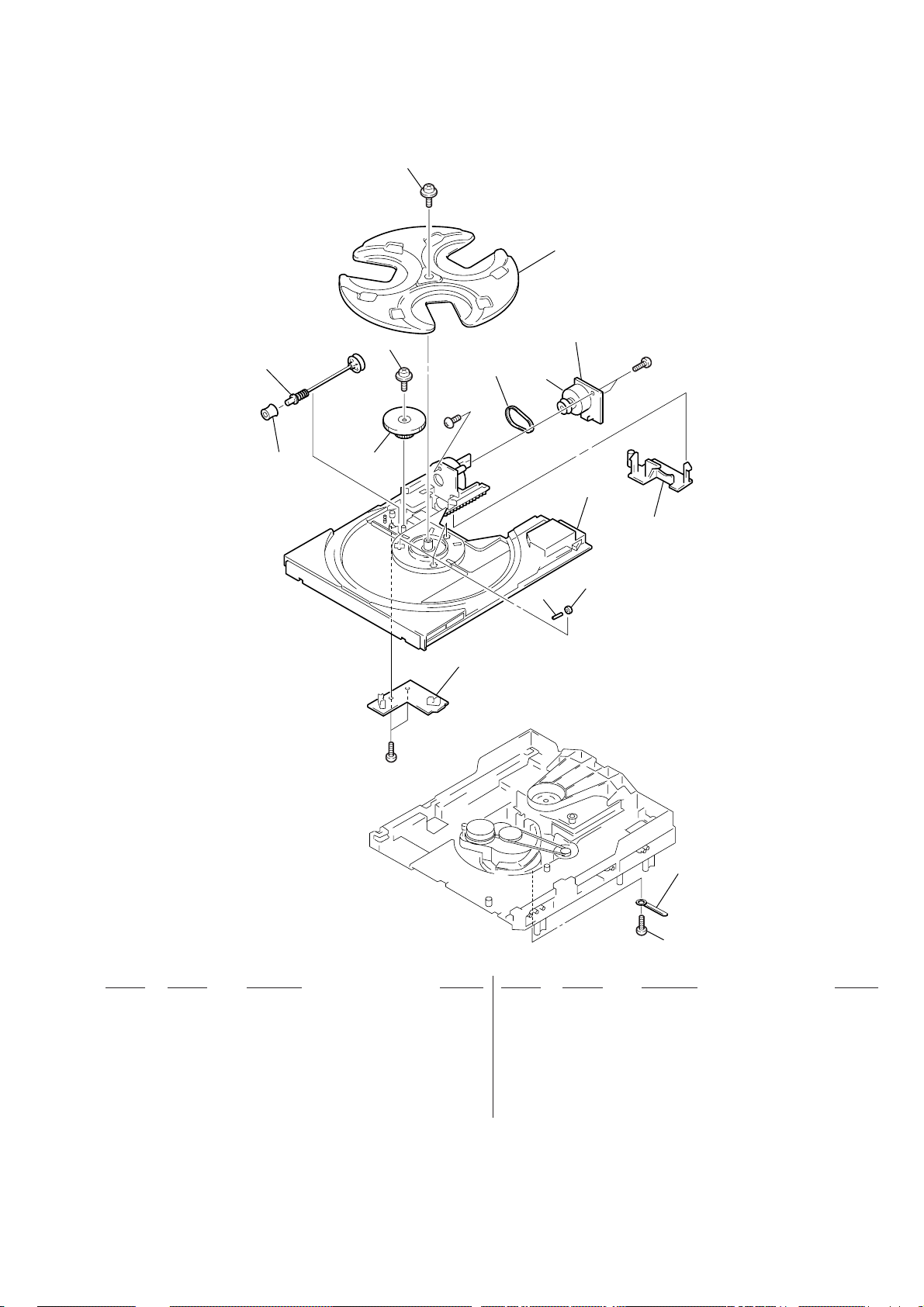
7-3. CD MECHANISM DECK SECTION-1
d
(CDM38-5BD21)
201
202
203
211
205
201
#2
#4
209
204
M701
210
206
#1
212
208
207
not supplie
213
Ref. No.Part No. Description Remarks Ref. No.Part No. Description Remarks
201 4-917-583-71BRACKET, YOKE
202 4-977-945-01TRAY (TURN)
203 X-4946-665-1SHAFT ASSY, WORM
204 4-977-943-01BELT (TURN) (1.2)
205 4-977-956-01WHEEL, WORM
* 206 1-658-577-11MOTOR (TURN) BOARD
207 X-4924-457-1ROLLER ASSY
208 4-977-941-01BEARING (WORM)
* 209 1-658-576-11SENSOR BOARD
210 4-934-376-01SHAFT (ROLLER)
211 4-981-187-01COLLAR (WORM)
212 4-977-944-01TRAY (SLIDE)
213 4-951-620-01SCREW (2.6X8), +BVTP
M701 A-4672-004-AMOTOR ASSY (TURN)
— 71 —
Page 34

7-4. CD MECHANISM DECK SECTION-2
(CDM38-5BD21)
251
261
BU-5BD21
258
259
#1
not supplied
254
#1
251
261
S811
253
252
256
M801
255
257
260
262
263
263
#2
264
265
251
Ref. No.Part No. Description Remarks Ref. No.Part No. Description Remarks
251 4-917-583-71BRACKET, YOKE (IA,TH)
252 4-977-954-01PULLEY (SL)
253 4-977-953-01GEAR (SL-A)
254 4-977-955-01GEAR (SL-B)
255 4-977-942-01BELT (SL) (1.4)
256 X-4946-667-1CAM ASSY, BU
257 1-452-925-11MAGNET ASSY
258 1-776-042-11WIRE (FLAT TYPE) (8 CORE)
* 259 1-658-575-11CONNECTOR, BOARD
* 260 X-4946-668-1CHASSIS (CDM) ASSY
261 4-985-672-01SCREW (+PTPWHM2.6), FLOATING
* 262 1-658-578-11MOTOR (SLIDE) BOARD
263 4-982-447-01SPRING (BU), COMPRESSION
264 4-951-620-41SCREW (2.6), +BVTP
* 265 X-4946-666-1HOLDER (BU) ASSY
M801 A-4672-004-AMOTOR ASSY (SLED)
S811 1-473-335-11ENCODER, ROTARY (BU, TRAY ADDRESS DET)
— 72 —
Page 35
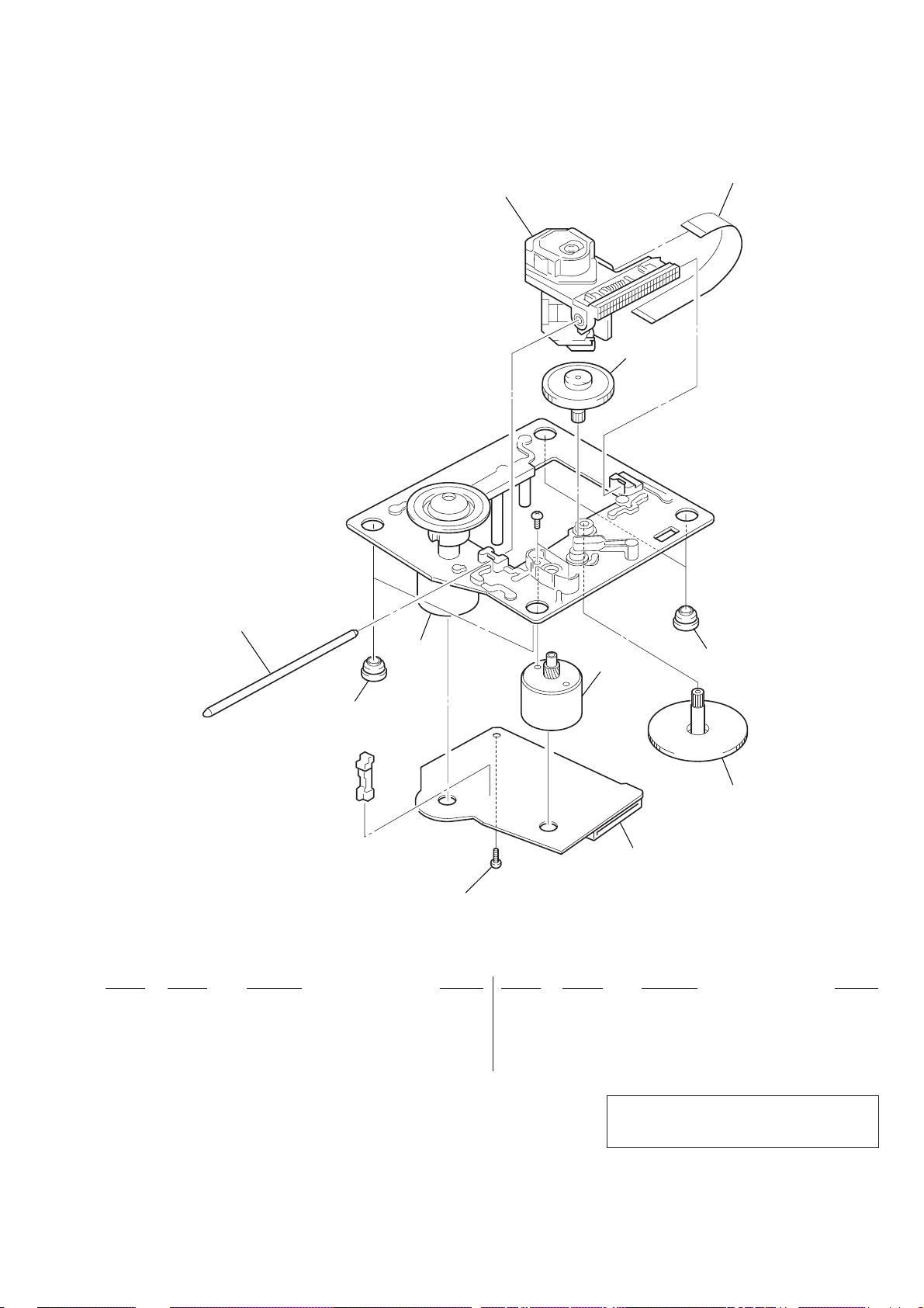
7-5. BASE UNIT SECTION
(BU-5BD21)
305
M101
301
#6
M102
302
303
304
304
306
307
308
Ref. No.Part No. Description Remarks Ref. No.Part No. Description Remarks
! 301 8-848-379-31OPTICAL PICK-UP KSS-213B/S-N
302 1-769-069-11WIRE (FLAT TYPE) (16 CORE)
303 4-917-567-01GEAR (M)
304 4-951-940-01INSULATOR (BU)
305 4-917-565-01SHAFT, SLED
306 4-917-564-01GEAR (P), FLATNESS
307 A-4673-557-ABD (A) BOARD, COMPLETE
308 4-951-620-01SCREW (2.6X8), +BVTP
M101 X-4917-523-3MOTOR ASSY (SPRING)
M102 X-4917-504-1MOTOR ASSY (SLED)
The components identified by mark ! or dotted
line with mark ! are critical for safety.
Replace only with part number specified.
— 73 —
Page 36

7-6. TAPE MECHANISM DECK SECTION-1
8
(TCM-220WR2E)
#8
HP101
(including
356
355
354
352
not supplied
●
A)
not supplied
351
357
#7
#9
359
374
362
358
not supplied
HRPE101
(including
353
364
360
355
356
365
●
B)
361
373
370
366
363
367
not supplied
359
357
371
364
368
372
(including ●C)
●
A
●
A
371
#
●
B
365
#9
369
366
362
361
370
●
371
363
374
B
#9
not supplied
354
not supplied
360
358
353
351
352
Ref. No.Part No. Description Remarks Ref. No.Part No. Description Remarks
351 3-908-560-01SPRING, AZIMUTH ADJUSTMENT
352 3-919-684-01SCREW, AZIMUTH ADJUSTMENT
353 X-3373-113-1SLIDER (HEAD) ASSY
354 3-908-556-01SPRING, HEAD TOGGLE
355 3-908-558-02FITTING BLOCK, HEAD
356 3-908-557-02ROTARY BLOCK, HEAD
* 357 3-908-559-01STOPPER, AZIMUTH
358 3-908-555-01SLIDER (REV SLIDER)
359 3-917-143-11SPRING, TENSION
360 3-388-848-01SCREW (P2X6) (B TIGHT)
361 3-939-371-01SPRING (1), TENSION
362 X-3369-909-1PINCH LEVER (REV) ASSY
363 X-3369-908-1PINCH LEVER (FWD) ASSY
#7
not supplied
364 3-908-613-01GEAR (S), REEL
365 3-917-141-01SPRING, COMPRESSION
366 X-3371-305-1REEL (T) ASSY
367 3-669-465-01W ASHER (1.5), STOPPER
368 X-3370-173-1TU ASSY
* 369 4-980-439-01FULCRUM, HOLDER
370 3-917-142-01SPRING, COMPRESSION
371 3-939-862-01CLIP
* 372 A-2007-435-AAUDIO BOARD, COMPLETE
373 3-930-972-01DETENT, HALF
374 3-354-963-01DAMPER
HP101 1-500-093-11HEAD, MAGNETIC (PLAYBACK)(DECK A)
HRPE1011-500-094-11HEAD, MAGNETIC (REC/PB/ERASE)(DECK B)
— 74 —
Page 37

7-7. TAPE MECHANISM DECK SECTION-2
(TCM-220WR2E)
• C: MOTOR board
418
419
●
C
M2
413
423
409
402
417
414
#7
M1
416
415
407
413
not supplied
420
412
410
424
411
A
408
#5
410
407
405
404
A
403
406
#11
419
#12
421
#11
421
#10
#10
Ref. No.Part No. Description Remarks Ref. No.Part No. Description Remarks
401 3-908-597-01CAM (A)
402 3-908-608-11SCREW, STEP
403 X-3372-930-1ARM (A) ASSY, FR
404 X-3370-169-1FLYWHEEL (AR) ASSY
405 3-928-047-01PULLEY, TENSION
406 3-908-599-01LEVER (REV-A)
407 3-908-601-01SPRING (REV LEVER), TORSION
408 3-908-603-01LEVER (TRIGGER A)
409 X-3367-593-1FLYWHEEL (BF) ASSY
410 3-908-605-01SPRING (TRIGGER), TORSION
411 3-908-609-01GEAR, TRIGGER
412 3-913-845-11BELT (A)
413 3-913-846-11BELT (FR)
414 X-3370-171-1FLYWHEEL (BR) ASSY
415 3-908-600-01LEVER (REV-B)
* 416 1-650-669-11LEAF SWITCH BOARD
417 3-908-598-01CAM (B)
418 X-3372-931-1ARM (B) ASSY, FR
419 3-911-114-01SPRING (FR), TORSION
420 3-908-604-01LEVER (TRIGGER B)
421 3-911-115-01W ASHER, STOPPER
423 3-917-176-11BELT (B)
424 X-3370-172-1FLYWHEEL (AF) ASSY
M1 A-2004-409-AMOTOR ASSY, CAPSTAN
M2 A-2004-410-AMOTOR ASSY, DC
402
401
— 75 —
Page 38

AUDIO
SECTION 8
ELECTRICAL PARTS LIST
Note:
When indicating parts by reference number,
please include the board name.
The components identified by mark ! or
dotted line with mark ! are critical for safety .
Replace only with part number specified.
• Abbreviation
MY: Malaysia CH : Chinese
SP : Singapore TH : Thai
HK : Hong Kong IA : Indonesian
KR : Korean
Ref. No.Part No. Description Remarks Ref. No.Part No. Description Remarks
* A-2007-435-AAUDIO BOARD, COMPLETE
**********************
< CAPACITOR >
C301 1-162-289-31CERAMIC 390PF 10% 50V
C302 1-126-968-11ELECT 100uF 20% 6.3V
C303 1-162-282-31CERAMIC 100PF 10% 50V
C304 1-130-483-00MYLAR 0.01uF 5% 50V
C305 1-107-715-11ELECT 22uF 20% 16V
C311 1-162-289-31CERAMIC 390PF 10% 50V
C313 1-162-282-31CERAMIC 100PF 10% 50V
C314 1-130-487-00MYLAR 0.022uF 5% 50V
C315 1-126-233-11ELECT 22uF 20% 50V
C331 1-137-427-11FILM 120PF 5% 50V
C332 1-162-288-31CERAMIC 330PF 10% 50V
C333 1-162-209-31CERAMIC 27PF 5% 50V
C401 1-162-289-31CERAMIC 390PF 10% 50V
C402 1-126-968-11ELECT 100uF 20% 6.3V
C403 1-162-282-31CERAMIC 100PF 10% 50V
C404 1-130-483-00MYLAR 0.01uF 5% 50V
C405 1-107-715-11ELECT 22uF 20% 16V
C411 1-162-289-31CERAMIC 390PF 10% 50V
C413 1-162-282-31CERAMIC 100PF 10% 50V
C414 1-130-487-00MYLAR 0.022uF 5% 50V
C415 1-126-233-11ELECT 22uF 20% 50V
C431 1-137-427-11FILM 120PF 5% 50V
C432 1-162-288-31CERAMIC 330PF 10% 50V
C433 1-162-209-31CERAMIC 27PF 5% 50V
C601 1-104-396-11ELECT 10uF 20% 16V
C602 1-104-396-11ELECT 10uF 20% 16V
C611 1-124-907-11ELECT 10uF 20% 50V
C612 1-124-907-11ELECT 10uF 20% 50V
C621 1-137-150-11FILM 0.01uF 5% 100V
C622 1-126-961-11ELECT 2.2uF 20% 50V
C623 1-136-155-00FILM 0.015uF 5% 50V
C624 1-130-481-00MYLAR 0.0068uF5% 50V
C625 1-130-481-00MYLAR 0.0068uF5% 50V
C627 1-124-903-11ELECT 1uF 20% 50V
C628 1-136-153-00FILM 0.01uF 5% 50V
C642 1-104-664-11ELECT 47uF 20% 16V
C651 1-161-494-00CERAMIC 0.022uF 25V
< CONNECTOR >
• Due to standardization, replacements in the
parts list may be different from the parts
specified in the diagrams or the components
used on the set.
• -XX, -X mean standardized parts, so they may
have some difference from the original one.
• Items marked “*” are not stocked since they
are seldom required for routine service. Some
delay should be anticipated when ordering these
items.
• CAP ACIT ORS:
uF: µF
IC601 8-759-111-44IC uPC4570C-1
IC601 8-759-710-59IC NJM4580D-D
IC602 8-759-143-54IC uPC1330HA
IC611 8-759-111-44IC uPC4570C-1
IC611 8-759-710-59IC NJM4580D-D
L331 1-410-780-11INDUCTOR 27mH
L431 1-410-780-11INDUCTOR 27mH
Q621 8-729-142-46TRANSISTOR 2SC2001-LK
Q622 8-729-142-46TRANSISTOR 2SC2001-LK
Q623 8-729-030-18TRANSISTOR 2SD2525
Q651 8-729-900-65TRANSISTOR DTA144ES
R301 1-247-881-00CARBON 120K 5% 1/4W
R302 1-249-409-11CARBON 220 5% 1/4W F
R303 1-249-433-11CARBON 22K 5% 1/4W
R304 1-247-889-00CARBON 270K 5% 1/4W
R305 1-247-858-11CARBON 13K 5% 1/4W
R311 1-247-881-00CARBON 120K 5% 1/4W
R312 1-247-807-31CARBON 100 5% 1/4W
R314 1-247-882-11CARBON 130K 5% 1/4W
R315 1-247-850-11CARBON 6.2K 5% 1/4W
R331 1-249-430-11CARBON 12K 5% 1/4W
R401 1-247-881-00CARBON 120K 5% 1/4W
R402 1-249-409-11CARBON 220 5% 1/4W F
R403 1-249-433-11CARBON 22K 5% 1/4W
R404 1-247-889-00CARBON 270K 5% 1/4W
R405 1-247-858-11CARBON 13K 5% 1/4W
R411 1-247-881-00CARBON 120K 5% 1/4W
R412 1-247-807-31CARBON 100 5% 1/4W
R414 1-247-882-11CARBON 130K 5% 1/4W
R415 1-247-850-11CARBON 6.2K 5% 1/4W
R431 1-249-430-11CARBON 12K 5% 1/4W
R601 1-249-409-11CARBON 220 5% 1/4W F
R602 1-249-409-11CARBON 220 5% 1/4W F
R608 1-249-409-11CARBON 220 5% 1/4W F
R609 1-249-433-11CARBON 22K 5% 1/4W
R611 1-249-409-11CARBON 220 5% 1/4W F
• RESISTORS
All resistors are in ohms.
METAL: metal-film resistor
METAL OXIDE: Metal Oxide-film resistor
F: nonflammable
• COILS
uH: µH
• SEMICONDUCTORS
In each case, u: µ, for example:
uA...: µA... , uPA... , µPA... ,
uPB... , µPB... , uPC... , µPC... ,
uPD..., µPD...
< IC >
< COIL >
< TRANSISTOR >
< RESISTOR >
CN601 1-695-382-31PIN, CONNECTOR (PC BOARD) 21P
CN602 1-564-718-11PIN, CONNECTOR (SMALL TYPE) 2P
* CN651 1-564-521-11PLUG, CONNECTOR 6P
R612 1-249-409-11CARBON 220 5% 1/4W F
! R621 1-212-851-00FUSIBLE 5.6 5% 1/4W F
! R622 1-212-851-00FUSIBLE 5.6 5% 1/4W F
R623 1-249-432-11CARBON 18K 5% 1/4W
R624 1-249-432-11CARBON 18K 5% 1/4W
— 76 —
Page 39

AUDIO BD CD PANEL
Ref. No.Part No. Description Remarks Ref. No.Part No. Description Remarks
R625 1-249-429-11CARBON 10K 5% 1/4W
R651 1-247-856-00CARBON 11K 5% 1/4W
R652 1-247-856-00CARBON 11K 5% 1/4W
R653 1-249-441-11CARBON 100K 5% 1/4W
< VARIABLE RESISTOR >
RV301 1-238-598-11RES, ADJ, CARBON 2.2K
RV311 1-238-598-11RES, ADJ, CARBON 2.2K
RV341 1-238-551-11RES, ADJ, CARBON 220K
RV401 1-238-598-11RES, ADJ, CARBON 2.2K
RV411 1-238-598-11RES, ADJ, CARBON 2.2K
RV441 1-238-551-11RES, ADJ, CARBON 220K
RV651 1-238-599-11RES, ADJ, CARBON 4.7K
RV652 1-238-599-11RES, ADJ, CARBON 4.7K
< TRANSFORMER >
T621 1-423-980-11TRANSFORMER, BIAS OSCILLATION
************************************************************
* A-4673-557-ABD BOARD, COMPLETE
*******************
< CAPACITOR >
C101 1-163-005-11CERAMIC CHIP 470PF 10% 50V
C102 1-163-038-91CERAMIC CHIP 0.1uF 25V
C103 1-163-005-11CERAMIC CHIP 470PF 10% 50V
C105 1-104-913-11TANTAL. CHIP 10uF 20% 16V
C106 1-164-346-11CERAMIC CHIP 1uF 16V
C107 1-164-346-11CERAMIC CHIP 1uF 16V
C108 1-163-035-00CERAMIC CHIP 0.047uF 50V
C109 1-163-145-00CERAMIC CHIP 0.0015uF5% 50V
C110 1-163-017-00CERAMIC CHIP 0.0047uF5% 50V
C111 1-163-251-11CERAMIC CHIP 100PF 5% 50V
C112 1-163-038-91CERAMIC CHIP 0.1uF 25V
C113 1-163-038-91CERAMIC CHIP 0.1uF 25V
C115 1-126-607-11ELECT CHIP 47uF 20% 4V
C116 1-126-607-11ELECT CHIP 47uF 20% 4V
C117 1-126-209-11ELECT 100uF 20% 4V
C118 1-163-275-11CERAMIC CHIP 0.001uF 5% 50V
C119 1-163-235-11CERAMIC CHIP 22PF 5% 50V
C123 1-164-232-11CERAMIC CHIP 0.01uF 50V
C124 1-164-005-11CERAMIC CHIP 0.47uF 25V
C125 1-104-913-11TANTAL. CHIP 10uF 20% 16V
C140 1-163-038-91CERAMIC CHIP 0.1uF 25V
C141 1-163-038-91CERAMIC CHIP 0.1uF 25V
C151 1-163-237-11CERAMIC CHIP 27PF 5% 50V
C153 1-163-038-91CERAMIC CHIP 0.1uF 25V
C154 1-164-336-11CERAMIC CHIP 0.33uF 25V
C156 1-163-237-11CERAMIC CHIP 27PF 5% 50V
C157 1-163-145-00CERAMIC CHIP 0.0015uF5% 50V
C159 1-163-019-00CERAMIC CHIP 0.0068uF10% 50V
C161 1-163-038-91CERAMIC CHIP 0.1uF 25V
Q101 8-729-010-08TRANSISTOR MSB710-R
R101 1-216-077-00METAL CHIP 15K 5% 1/10W
R102 1-216-097-91METAL GLAZE 100K 5% 1/10W
R103 1-216-077-00METAL CHIP 15K 5% 1/10W
R104 1-216-085-00METAL CHIP 33K 5% 1/10W
R105 1-216-097-91METAL GLAZE 100K 5% 1/10W
R106 1-216-061-00METAL CHIP 3.3K 5% 1/10W
R107 1-216-061-00METAL CHIP 3.3K 5% 1/10W
R108 1-216-073-00METAL CHIP 10K 5% 1/10W
R109 1-216-121-91METAL GLAZE 1M 5% 1/10W
R110 1-216-025-91METAL GLAZE 100 5% 1/10W
R112 1-216-049-91METAL GLAZE 1K 5% 1/10W
R123 1-216-073-00METAL CHIP 10K 5% 1/10W
R124 1-216-097-91METAL GLAZE 100K 5% 1/10W
R125 1-216-033-00METAL CHIP 220 5% 1/10W
R126 1-216-033-00METAL CHIP 220 5% 1/10W
R127 1-216-033-00METAL CHIP 220 5% 1/10W
R131 1-216-037-00METAL CHIP 330 5% 1/10W
R132 1-216-073-00METAL CHIP 10K 5% 1/10W
R134 1-216-049-91METAL GLAZE 1K 5% 1/10W
R135 1-216-295-91CONDUCTOR, CHIP (2012)
R136 1-216-295-91CONDUCTOR, CHIP (2012)
R137 1-216-295-91CONDUCTOR, CHIP (2012)
R138 1-216-295-91CONDUCTOR, CHIP (2012)
R141 1-216-089-91METAL GLAZE 47K 5% 1/10W
R142 1-216-081-00METAL CHIP 22K 5% 1/10W
R143 1-216-103-00METAL CHIP 180K 5% 1/10W
R144 1-216-103-00METAL CHIP 180K 5% 1/10W
R146 1-216-073-00METAL CHIP 10K 5% 1/10W
R147 1-216-067-00METAL CHIP 5.6K 5% 1/10W
R148 1-216-001-00METAL CHIP 10 5% 1/10W
R149 1-216-003-11METAL GLAZE 12 5% 1/10W
R158 1-216-109-00METAL CHIP 330K 5% 1/10W
R159 1-216-101-00METAL CHIP 150K 5% 1/10W
R160 1-216-295-91CONDUCTOR, CHIP (2012)
R161 1-216-308-00METAL CHIP 4.7 5% 1/10W
R162 1-216-101-00METAL CHIP 150K 5% 1/10W
S101 1-572-085-11SWITCH, LEAF (LIMIT)
************************************************************
* A-4403-280-ACD PANEL BOARD, COMPLETE
CNL102 1-568-860-21SOCKET, CONNECTOR 17P
< TRANSISTOR >
< RESISTOR >
< SWITCH >
*************************
< CONNECTOR >
< CONNECTOR >
CN101 1-774-115-11CONNECTOR, (FFC/FPC) 29P
CN102 1-770-014-11CONNECTOR, FFC/FPC 16P
< IC >
IC101 8-752-369-78IC CXD2545Q
IC102 8-759-176-09IC BA6392FP
IC103 8-752-072-45IC CXA1821M-T6
< DIODE >
D211 8-719-812-44DIODE TLO124
D212 8-719-812-44DIODE TLO124
D213 8-719-033-06DIODE SEL5920A
D214 8-719-033-06DIODE SEL5920A
D215 8-719-032-86DIODE SEL5420E
— 77 —
Page 40

LEAF SWITCHCONNECTORCD PANEL
Ref. No.Part No. Description Remarks Ref. No.Part No. Description Remarks
D216 8-719-032-86DIODE SEL5420E
D217 8-719-056-13DIODE SML79423C-TP15 (DISC 1)
D218 8-719-056-13DIODE SML79423C-TP15 (DISC 1)
D219 8-719-056-13DIODE SML79423C-TP15 (DISC 1)
D220 8-719-056-13DIODE SML79423C-TP15 (DISC 2)
R280 1-216-025-91METAL GLAZE 100 5% 1/10W
R281 1-216-029-00METAL CHIP 150 5% 1/10W
R282 1-216-029-00METAL CHIP 150 5% 1/10W
R283 1-216-033-00METAL CHIP 220 5% 1/10W
R284 1-216-037-00METAL CHIP 330 5% 1/10W
D221 8-719-056-13DIODE SML79423C-TP15 (DISC 2)
D222 8-719-056-13DIODE SML79423C-TP15 (DISC 2)
D223 8-719-056-13DIODE SML79423C-TP15 (DISC 3)
D224 8-719-056-13DIODE SML79423C-TP15 (DISC 3)
D225 8-719-056-13DIODE SML79423C-TP15 (DISC 3)
D226 8-719-056-13DIODE SML79423C-TP15 (^)
D227 8-719-056-13DIODE SML79423C-TP15 (^)
< TRANSISTOR >
Q205 8-729-027-23TRANSISTOR DTA114EKA-T146
Q206 8-729-027-23TRANSISTOR DTA114EKA-T146
Q207 8-729-027-23TRANSISTOR DTA114EKA-T146
Q208 8-729-027-23TRANSISTOR DTA114EKA-T146
Q209 8-729-027-23TRANSISTOR DTA114EKA-T146
Q210 8-729-027-23TRANSISTOR DTA114EKA-T146
Q211 8-729-027-23TRANSISTOR DTA114EKA-T146
Q212 8-729-027-23TRANSISTOR DTA114EKA-T146
Q213 8-729-027-23TRANSISTOR DTA114EKA-T146
Q214 8-729-027-23TRANSISTOR DTA114EKA-T146
Q215 8-729-027-23TRANSISTOR DTA114EKA-T146
Q216 8-729-027-23TRANSISTOR DTA114EKA-T146
Q217 8-729-027-23TRANSISTOR DTA114EKA-T146
Q218 8-729-027-23TRANSISTOR DTA114EKA-T146
< RESISTOR >
R285 1-216-041-00METAL CHIP 470 5% 1/10W
R286 1-216-045-00METAL CHIP 680 5% 1/10W
R287 1-216-049-91METAL GLAZE 1K 5% 1/10W
R288 1-216-053-00METAL CHIP 1.5K 5% 1/10W
R289 1-216-057-00METAL CHIP 2.2K 5% 1/10W
< SWITCH >
S270 1-762-750-11SWITCH, TACTILE (fl CD NON-STOP)
S271 1-762-750-11SWITCH, TACTILE (6 OPEN/CLOSE)
S272 1-762-750-11SWITCH, TACTILE (p)
S273 1-762-750-11SWITCH, TACTILE (SELECT)
S274 1-762-750-11SWITCH, TACTILE (DISC 3)
S275 1-762-750-11SWITCH, TACTILE (DISC 2)
S276 1-762-750-11SWITCH, TACTILE (DISC 1)
S277 1-762-750-11SWITCH, TACTILE (RETURN)
S278 1-762-750-11SWITCH, TACTILE ())
S279 1-762-750-11SWITCH, TACTILE (0)
S280 1-762-750-11SWITCH, TACTILE (DISC SKIP EX-CHANGE)
S281 1-762-750-11SWITCH, TACTILE (PREV)
S282 1-762-750-11SWITCH, TACTILE (NEXT)
************************************************************
* 1-658-575-11CONNECTOR, BOARD
*****************
< CONNECTOR >
R234 1-216-033-00METAL CHIP 220 5% 1/10W
R235 1-216-033-00METAL CHIP 220 5% 1/10W
R236 1-216-033-00METAL CHIP 220 5% 1/10W
R237 1-216-033-00METAL CHIP 220 5% 1/10W
R238 1-216-033-00METAL CHIP 220 5% 1/10W
R239 1-216-033-00METAL CHIP 220 5% 1/10W
R244 1-216-033-00METAL CHIP 220 5% 1/10W
R245 1-216-033-00METAL CHIP 220 5% 1/10W
R246 1-216-033-00METAL CHIP 220 5% 1/10W
R247 1-216-033-00METAL CHIP 220 5% 1/10W
R248 1-216-033-00METAL CHIP 220 5% 1/10W
R249 1-216-033-00METAL CHIP 220 5% 1/10W
R254 1-216-033-00METAL CHIP 220 5% 1/10W
R255 1-216-033-00METAL CHIP 220 5% 1/10W
R256 1-216-033-00METAL CHIP 220 5% 1/10W
R257 1-216-033-00METAL CHIP 220 5% 1/10W
R258 1-216-033-00METAL CHIP 220 5% 1/10W
R259 1-216-033-00METAL CHIP 220 5% 1/10W
R264 1-216-033-00METAL CHIP 220 5% 1/10W
R265 1-216-033-00METAL CHIP 220 5% 1/10W
R266 1-216-033-00METAL CHIP 220 5% 1/10W
R267 1-216-033-00METAL CHIP 220 5% 1/10W
R268 1-216-033-00METAL CHIP 220 5% 1/10W
R269 1-216-033-00METAL CHIP 220 5% 1/10W
R274 1-216-033-00METAL CHIP 220 5% 1/10W
R275 1-216-033-00METAL CHIP 220 5% 1/10W
R276 1-216-033-00METAL CHIP 220 5% 1/10W
R277 1-216-033-00METAL CHIP 220 5% 1/10W
R278 1-216-017-91METAL GLAZE 47 5% 1/10W
R279 1-216-021-00METAL CHIP 68 5% 1/10W
* CN701 1-568-946-11PIN, CONNECTOR 8P
CN702 1-750-413-11CONNECTOR, FFC/FPC 8P
< TRANSISTOR >
Q701 8-729-900-80TRANSISTOR DTC114ES
< RESISTOR >
R703 1-249-435-11CARBON 33K 5% 1/4W
R704 1-249-429-11CARBON 10K 5% 1/4W
R705 1-249-417-11CARBON 1K 5% 1/4W F
************************************************************
* 1-650-669-11LEAF SWITCH BOARD
*****************
< CONNECTOR >
* CN1001 1-568-854-11SOCKET, CONNECTOR 11P
CN1001 1-695-372-31PIN, CONNECTOR (PC BOARD) 11P
< TRANSISTOR >
Q1001 8-749-010-90TRANSISTOR PHOTO REFLECTOR
NJL5165KA-H
Q1002 8-749-010-90TRANSISTOR PHOTO REFLECTOR
NJL5165KA-H
< RESISTOR >
R1001 1-247-818-11CARBON 300 5% 1/4W
R1002 1-247-820-11CARBON 360 5% 1/4W
R1003 1-249-414-11CARBON 560 5% 1/4W F
R1004 1-247-834-11CARBON 1.3K 5% 1/4W
R1005 1-247-818-11CARBON 300 5% 1/4W
— 78 —
Page 41

MAINLEAF SWITCH
Ref. No.Part No. Description Remarks Ref. No.Part No. Description Remarks
< SWITCH >
S1001 1-692-832-11SWITCH, PUSH (1 KEY) (A PLAY)
S1002 1-692-832-11SWITCH, PUSH (1 KEY) (B PLAY)
S1004 1-571-281-21SWITCH, LEAF (A HALE)
S1005 1-571-281-21SWITCH, LEAF (A CrO2)
S1006 1-572-248-11SWITCH, LEAF (REC A)
S1007 1-572-248-11SWITCH, LEAF (B HALE)
S1008 1-571-281-21SWITCH, LEAF (B CrO2)
S1009 1-571-281-21SWITCH, LEAF (REC B)
************************************************************
* A-4403-279-AMAIN BOARD, COMPLETE (MY,SP,KR,HK,CH)
*********************
* A-4403-712-AMAIN BOARD, COMPLETE (TH)
*********************
* A-4403-716-AMAIN BOARD, COMPLETE (IA)
*********************
< CAPACITOR >
C001 1-164-159-11CERAMIC 0.1uF 50V
(MY,SP,KR,HK,CH)
C127 1-162-282-31CERAMIC 100P 10% 50V
C128 1-162-306-11CERAMIC 0.01uF 20% 16V
C129 1-126-933-11ELECT 100uF 20% 10V
C130 1-162-282-31CERAMIC 100P 10% 50V
C131 1-164-159-11CERAMIC 0.1uF 20% 50V
(MY,SP,KR,HK,CH)
C132 1-164-159-11CERAMIC 0.1uF 20% 50V
(MY,SP,KR,HK,CH)
C133 1-164-159-11CERAMIC 0.1uF 20% 50V
C134 1-164-159-11CERAMIC 0.1uF 20% 50V
(MY,SP,KR,HK,CH)
C135 1-162-290-31CERAMIC 150P 10% 50V
(MY,SP,KR,HK,CH)
C136 1-162-290-31CERAMIC 220P 10% 50V
(MY,SP,KR,HK,CH)
C137 1-164-159-11CERAMIC 0.1uF 20% 50V
C138 1-126-933-11ELECT 100uF 20% 10V
C139 1-128-551-11ELECT 22uF 20% 25V
C140 1-164-159-11CERAMIC 0.1uF 20% 50V
(MY,SP,KR,HK,CH)
C402 1-162-600-11CERAMIC 0.0047uF30% 16V
C403 1-162-290-31CERAMIC 470PF 10% 50V
C405 1-126-301-11ELECT 1uF 20% 50V
C406 1-137-399-11FILM 0.1uF 5% 50V
C407 1-126-964-11ELECT 10uF 20% 50V
C409 1-126-964-11ELECT 10uF 20% 50V
C411 1-126-301-11ELECT 1uF 20% 50V
C421 1-126-964-11ELECT 10uF 20% 50V
C422 1-126-964-11ELECT 10uF 20% 50V
C423 1-126-933-11ELECT 100uF 20% 10V
C424 1-164-159-11CERAMIC 0.1uF 20% 50V
(MY,SP,KR,HK,CH)
C425 1-164-159-11CERAMIC 0.1uF 20% 50V
(MY,SP,KR,HK,CH)
C426 1-164-159-11CERAMIC 0.1uF 20% 50V
(MY,SP,KR,HK,CH)
C427 1-126-935-11ELECT 470uF 20% 16V
C428 1-126-933-11ELECT 100uF 20% 16V
C429 1-126-933-11ELECT 100uF 20% 10V
C452 1-162-600-11CERAMIC 0.0047uF30% 16V
C453 1-162-290-31CERAMIC 470PF 10% 50V
C455 1-126-301-11ELECT 1uF 20% 50V
C456 1-137-399-11FILM 0.1uF 5% 50V
C457 1-126-964-11ELECT 10uF 20% 50V
C459 1-126-964-11ELECT 10uF 20% 50V
C461 1-126-301-11ELECT 1uF 20% 50V
C702 1-126-961-11ELECT 2.2uF 20% 50V
C752 1-126-961-11ELECT 2.2uF 20% 50V
C813 1-126-967-11ELECT 47uF 20% 10V
C853 1-126-944-11ELECT 3300uF 20% 25V
C854 1-126-944-11ELECT 3300uF 20% 25V
C861 1-126-768-11ELECT 2200uF 20% 16V
C862 1-126-933-11ELECT 100uF 20% 10V
C863 1-126-967-11ELECT 47uF 20% 10V
C867 1-126-967-11ELECT 47uF 20% 10V
C868 1-126-923-11ELECT 220uF 20% 10V
C869 1-126-967-11ELECT 47uF 20% 10V
C870 1-164-159-11CERAMIC 0.1uF 20% 50V
(MY,SP,KR.HK,CH)
C871 1-164-159-11CERAMIC 0.1uF 20% 50V
(MY,SP,KR,HK,CH)
C872 1-126-929-11ELECT 4700uF 20% 6.3V
C873 1-126-933-11ELECT 100uF 20% 10V
C876 1-126-933-11ELECT 100uF 20% 10V
< CONNECTOR >
* CN111 1-568-935-11PIN, CONNECTOR 8P
* CN112 1-568-936-11PIN, CONNECTOR 9P
* CNB108 1-764-017-31HOUSING,CONNECTOR(PC BOARD)17P
(SYSTEM CONT
< JACK >
CNJ106 1-770-721-11CONNECTOR, BOARD TO BOARD 4P
< CONNECTOR >
CNP105 1-770-393-11PIN, CONNECTOR (PC BOARD) 9P
CNS101 1-569-060-11SOCKET, CONNECTOR 11P
CNS102 1-568-440-11SOCKET, CONNECTOR 17P
CNS103 1-568-443-11SOCKET, CONNECTOR 13P
CNS104 1-569-324-11SOCKET, CONNECTOR 21P
< DIODE >
D110 8-719-987-63DIODE 1N4148M
D855 8-719-110-08DIODE RD8.2ES-B2 (MY,SP,KR,HK,CH)
D858 8-719-110-08DIODE RD8.2ES-B2 (MY,SP,KR,HK,CH)
D901 8-719-024-99DIODE 11ES2-NTA2B (MY,SP,KR,HK,CH)
D902 8-719-024-99DIODE 11ES2-NTA2B (MY,SP,KR,HK,CH)
D903 8-719-024-99DIODE 11ES2-NTA2B (MY,SP,KR,HK,CH)
D904 8-719-024-99DIODE 11ES2-NTA2B (MY,SP,KR,HK,CH)
< TERMINAL >
* EH01 1-537-738-21TERMINAL, EARTH
< IC >
IC101 8-759-482-60IC uPD780016YGF-016-3BA
IC103 8-759-165-82IC PST600E-T
IC107 8-749-921-12IC GP1F32T (OPTICAL DIGITAL OUT)
IC401 8-759-363-21IC HA12203NT
IC402 8-759-822-09IC LB1641
R
— 79 —
Page 42

MAIN
Ref. No.Part No. Description Remarks Ref. No.Part No. Description Remarks
J401 1-410-482-31INDUCTOR 100uH
MOTOR (SLIDE)
< JACK >
< TRANSISTOR >
R433 1-249-425-11CARBON 4.7K 5% 1/4W F
R434 1-249-425-11CARBON 4.7K 5% 1/4W F
R435 1-249-425-11CARBON 4.7K 5% 1/4W F
R436 1-249-417-11CARBON 1K 5% 1/4W F
R437 1-249-436-11CARBON 39K 5% 1/4W
Q102 8-729-040-20TRANSISTOR RT1P137L
Q103 8-729-900-80TRANSISTOR DTC114ES
Q104 8-729-040-20TRANSISTOR RT1P137L
Q105 8-729-040-20TRANSISTOR RT1P137L
Q106 8-729-029-66TRANSISTOR BA1A4M
Q405 8-729-801-93TRANSISTOR 2SD1387
Q408 8-729-900-80TRANSISTOR BA1A4M
Q409 8-729-900-80TRANSISTOR BA1A4M
Q410 8-729-119-76TRANSISTOR 2SA1175-HFE
Q411 8-729-900-80TRANSISTOR BA1A4M
Q852 8-729-018-60TRANSISTOR 2SD2012-LC
Q855 8-729-018-59TRANSISTOR 2SB1375-LC
< RESISTOR >
R130 1-247-807-31CARBON 100 5% 1/4W
R131 1-247-807-31CARBON 100 5% 1/4W
R132 1-247-807-31CARBON 100 5% 1/4W
R133 1-247-807-31CARBON 100 5% 1/4W
R134 1-247-807-31CARBON 100 5% 1/4W
R135 1-247-807-31CARBON 100 5% 1/4W
R136 1-247-807-31CARBON 100 5% 1/4W
R139 1-249-429-11CARBON 10K 5% 1/4W
R140 1-249-429-11CARBON 10K 5% 1/4W
R141 1-249-429-11CARBON 10K 5% 1/4W
R142 1-249-429-11CARBON 10K 5% 1/4W
R143 1-247-807-31CARBON 100 5% 1/4W
R146 1-249-417-11CARBON 1K 5% 1/4W F
R147 1-249-429-11CARBON 10K 5% 1/4W
R148 1-249-429-11CARBON 10K 5% 1/4W
R438 1-249-436-11CARBON 39K 5% 1/4W
R439 1-249-437-11CARBON 47K 5% 1/4W
R440 1-249-437-11CARBON 47K 5% 1/4W
R442 1-247-843-11CARBON 3.3K 5% 1/4W
R447 1-249-411-11CARBON 330 5% 1/4W
R448 1-249-427-11CARBON 6.8K 5% 1/4W F
R449 1-249-429-11CARBON 10K 5% 1/4W
R450 1-249-425-11CARBON 4.7K 5% 1/4W F
R453 1-249-426-11CARBON 5.6K 5% 1/4W
R454 1-249-417-11CARBON 1K 5% 1/4W F
R455 1-247-840-00CARBON 2.4K 5% 1/4W
R456 1-249-421-11CARBON 2.2K 5% 1/4W F
R457 1-249-428-11CARBON 8.2K 5% 1/4W F
R459 1-249-433-11CARBON 22K 5% 1/4W
(MY,SP,KR,HK,CH)
R469 1-249-433-11CARBON 22K 5% 1/4W
(MY,SP,KR,HK,CH)
R470 1-249-425-11CARBON 4.7K 5% 1/4W F
R480 1-249-430-11CARBON 12K 5% 1/4W
R704 1-249-417-11CARBON 1K 5% 1/4W F
R705 1-249-438-11CARBON 56K 5% 1/4W
R706 1-249-417-11CARBON 1K 5% 1/4W F
R754 1-249-417-11CARBON 1K 5% 1/4W F
R755 1-249-438-11CARBON 56K 5% 1/4W
R756 1-249-417-11CARBON 1K 5% 1/4W F
R855 1-249-417-11CARBON 1K 5% 1/4W F
R859 1-249-417-11CARBON 1K 5% 1/4W F
! R861 1-212-853-00FUSIBLE 6.8 5% 1/4W F
! R862 1-212-853-00FUSIBLE 6.8 5% 1/4W F
R149 1-247-807-31CARBON 100 5% 1/4W
R150 1-247-807-31CARBON 100 5% 1/4W
R151 1-247-807-31CARBON 100 5% 1/4W
R152 1-247-807-31CARBON 100 5% 1/4W
R153 1-249-419-11CARBON 1.5K 5% 1/4W F
R154 1-249-419-11CARBON 1.5K 5% 1/4W F
R155 1-249-427-11CARBON 6.8K 5% 1/4W F
R156 1-249-427-11CARBON 6.8K 5% 1/4W F
R157 1-249-429-11CARBON 10K 5% 1/4W
R158 1-249-429-11CARBON 10K 5% 1/4W
R161 1-247-807-31CARBON 100 5% 1/4W
R162 1-247-807-31CARBON 100 5% 1/4W
R403 1-249-426-11CARBON 5.6K 5% 1/4W
R404 1-249-417-11CARBON 1K 5% 1/4W F
R405 1-247-840-00CARBON 2.4K 5% 1/4W
R406 1-249-421-11CARBON 2.2K 5% 1/4W F
R407 1-249-428-11CARBON 8.2K 5% 1/4W F
R409 1-249-433-11CARBON 22K 5% 1/4W
(MY,SP,KR,HK,CH)
R419 1-249-435-11CARBON 33K 5% 1/4W
R422 1-249-441-11CARBON 100K 5% 1/4W
R423 1-249-432-11CARBON 18K 5% 1/4W
R424 1-249-429-11CARBON 10K 5% 1/4W
R425 1-249-429-11CARBON 10K 5% 1/4W
R426 1-249-429-11CARBON 10K 5% 1/4W
R429 1-249-426-11CARBON 5.6K 5% 1/4W
— 80 —
< VARIABLE RESISTOR >
RV401 1-238-598-11RES, ADJ, CARBON 2.2K
RV451 1-238-598-11RES, ADJ, CARBON 2.2K
< VIBRATOR >
X101 1-760-489-11VIBRATOR, CERAMIC (5MHz)
************************************************************
* 1-658-578-11MOTOR (SLIDE) BOARD
*******************
< CAPACITOR >
C801 1-162-306-11CERAMIC 0.01uF 20% 16V
C804 1-162-306-11CERAMIC 0.01uF 20% 16V
C805 1-126-964-11ELECT 10uF 20% 50V
< CONNECTOR >
* CN801 1-568-947-11PIN, CONNECTOR 9P
< DIODE >
D801 8-719-010-43DIODE UZ-5.6BSC
D804 8-719-987-63DIODE 1N4148M
D805 8-719-987-63DIODE 1N4148M
The components identified by mark ! or dotted
line with mark ! are critical for safety.
Replace only with part number specified.
Page 43

TC (A)MOTOR (SLIDE) SENSORMOTOR (TURN) RESISTOR TC (B)
Ref. No.Part No. Description Remarks Ref. No.Part No. Description Remarks
< IC >
IC801 8-759-274-09IC BA6286N
< RESISTOR >
R801 1-249-401-11CARBON 47 5% 1/4W F
* 1-658-576-11SENSOR BOARD
*************
< IC >
IC702 8-749-924-18IC PHOTO INTERRUPTER RPI-1391
IC703 8-749-924-30IC PHOTO REFLECTOR GP2S28
< SWITCH >
S801 1-762-527-11SWITCH, ROTARY (OPEN/CLOSE)
************************************************************
* 1-658-577-11MOTOR (TURN) BOARD
*******************
< CAPACITOR >
C701 1-162-306-11CERAMIC 0.01uF 20% 16V
C702 1-126-964-11ELECT 10uF 20% 50V
C705 1-162-306-11CERAMIC 0.01uF 20% 16V
< CONNECTOR >
CN703 1-750-413-11CONNECTOR, FFC/FPC 8P
CN704 1-506-469-11PIN, CONNECTOR 4P
< DIODE >
D701 8-719-010-23DIODE UZ-3.6BSB
< IC >
IC701 8-759-633-65IC M54641L
< RESISTOR >
R706 1-249-411-11CARBON 330 5% 1/4W
R707 1-249-401-11CARBON 47 5% 1/4W F
************************************************************
* 1-666-004-11RESISTOR BOARD
***************
< CAPACITOR >
C850 0.1uF
C851 1-164-159-11CERAMIC 0.1uF 50V
(MY,SP,KR,HK,CH)
C852 1-164-159-11CERAMIC 0.1uF 50V
(MY,SP,KR,HK,CH)
C865 1-126-967-11ELECT 47uF 20% 10V
C866 2200 25V
< RESISTOR >
R701 1-249-416-11CARBON 820 5% 1/4W F
R702 1-249-407-11CARBON 150 5% 1/4W F
************************************************************
* 1-666-007-11TC (A) BOARD
***********
< DIODE >
D207 8-719-058-03DIODE SEL5423E-TP15 (·)
D208 8-719-058-03DIODE SEL5423E-TP15 (·)
D209 8-719-058-03DIODE SEL5423E-TP15 (ª)
D210 8-719-058-03DIODE SEL5423E-TP15 (ª)
< TRANSISTOR >
Q203 8-729-027-23TRANSISTOR DTA114EKA-T146
Q204 8-729-027-23TRANSISTOR DTA114EKA-T146
< RESISTOR >
R213 1-216-061-00METAL CHIP 3.3K 5% 1/10W
R214 1-216-069-00METAL CHIP 6.8K 5% 1/10W
R215 1-216-077-00METAL CHIP 15K 5% 1/10W
R230 1-216-033-00METAL CHIP 220 5% 1/10W
R231 1-216-033-00METAL CHIP 220 5% 1/10W
R232 1-216-033-00METAL CHIP 220 5% 1/10W
R233 1-216-033-00METAL CHIP 220 5% 1/10W
< SWITCH >
S264 1-762-750-11SWITCH, TACTILE (π)
S265 1-762-750-11SWITCH, TACTILE (ª)
S266 1-762-750-11SWITCH, TACTILE (·)
************************************************************
* 1-666-008-11TC (B) BOARD
************
< JACK >
CNJ105 1-770-402-11HOUSING, CONNECTOR(PC BOARD)9P
< DIODE >
D851 8-719-987-63DIODE 1N4148M
D852 8-719-987-63DIODE 1N4148M
< IC >
IC851 8-759-231-58IC TA7812S
IC852 8-759-231-53IC TA7805S
IC853 8-759-604-86IC M5F7807L
< RESISTOR >
R864 1-216-377-11METAL OXIDE 4.7 5% 2W F
R865 1-216-377-11METAL OXIDE 4.7 5% 2W F
R866 1-216-377-11METAL OXIDE 4.7 5% 2W F
R867 1-216-377-11METAL OXIDE 4.7 5% 2W F
************************************************************
— 81 —
< DIODE >
D201 8-719-058-03DIODE SEL5423E-TP15 (·)
D202 8-719-058-03DIODE SEL5423E-TP15 (·)
D203 8-719-058-03DIODE SEL5423E-TP15 (ª)
D204 8-719-058-03DIODE SEL5423E-TP15 (ª)
< TRANSISTOR >
Q201 8-729-027-23TRANSISTOR DTA114EKA-T146
Q202 8-729-027-23TRANSISTOR DTA114EKA-T146
< RESISTOR >
R201 1-216-017-91METAL GLAZE 47 5% 1/10W
R202 1-216-021-00METAL CHIP 68 5% 1/10W
R224 1-216-033-00METAL CHIP 220 5% 1/10W
R225 1-216-033-00METAL CHIP 220 5% 1/10W
R226 1-216-033-00METAL CHIP 220 5% 1/10W
Page 44

TC PANEL VIDEOTC (B)
Ref. No.Part No. Description Remarks Ref. No.Part No. Description Remarks
R227 1-216-033-00METAL CHIP 220 5% 1/10W
< SWITCH >
S251 1-762-750-11SWITCH, TACTILE (·)
S252 1-762-750-11SWITCH, TACTILE (ª)
S253 1-762-750-11SWITCH, TACTILE (π)
************************************************************
* A-4398-496-ATC PANEL BOARD, COMPLETE
************************
C105 1-163-038-91CERAMIC CHIP 0.1uF 25V
C106 1-163-131-00CERAMIC CHIP 390PF 5% 50V
C107 1-163-113-00CERAMIC CHIP 68PF 5% 50V
C108 1-163-038-91CERAMIC CHIP 0.1uF 25V
C109 1-126-206-11ELECT CHIP 100uF 20% 6.3V
C121 1-163-038-91CERAMIC CHIP 0.1uF 25V
C122 1-163-091-00CERAMIC CHIP 8PF 50V
C123 1-163-091-00CERAMIC CHIP 8PF 50V
C124 1-163-038-91CERAMIC CHIP 0.1uF 25V
C125 1-163-038-91CERAMIC CHIP 0.1uF 25V
< DIODE >
D205 8-719-033-06DIODE SEL5920A (PAUSE P)
D206 8-719-812-44DIODE TLO124 (REC)
< TRANSISTOR >
Q219 8-729-027-23TRANSISTOR DTA114EKA-T146
Q220 8-729-027-23TRANSISTOR DTA114EKA-T146
< RESISTOR >
R203 1-216-025-91METAL GLAZE 100 5% 1/10W
R204 1-216-029-00METAL CHIP 150 5% 1/10W
R205 1-216-029-00METAL CHIP 150 5% 1/10W
R206 1-216-033-00METAL CHIP 220 5% 1/10W
R207 1-216-037-00METAL CHIP 330 5% 1/10W
R208 1-216-041-00METAL CHIP 470 5% 1/10W
R209 1-216-045-00METAL CHIP 680 5% 1/10W
R210 1-216-049-91METAL GLAZE 1K 5% 1/10W
R211 1-216-053-00METAL CHIP 1.5K 5% 1/10W
R212 1-216-057-00METAL CHIP 2.2K 5% 1/10W
R228 1-216-033-00METAL CHIP 220 5% 1/10W
R229 1-216-033-00METAL CHIP 220 5% 1/10W
< SWITCH >
S254 1-762-750-11SWITCH, TACTILE ())
S255 1-762-750-11SWITCH, TACTILE (0)
S256 1-762-750-11SWITCH, TACTILE (DIRECTION MODE)
S257 1-762-750-11SWITCH, TACTILE (PAUSE P)
S258 1-762-750-11SWITCH, TACTILE (REC)
S259 1-762-750-11SWITCH, TACTILE (HI-SPEED DUBBING)
S260 1-762-750-11SWITCH, TACTILE (CD SYNCHRO)
S261 1-762-750-11SWITCH, TACTILE (DOLBY NR)
S262 1-762-750-11SWITCH, TACTILE ())
S263 1-762-750-11SWITCH, TACTILE (0)
************************************************************
C126 1-163-038-91CERAMIC CHIP 0.1uF 25V
C127 1-163-017-00CERAMIC CHIP 0.0047uF5% 50V
C128 1-163-239-11CERAMIC CHIP 33PF 5% 50V
C129 1-163-239-11CERAMIC CHIP 33PF 5% 50V
C131 1-164-159-21CERAMIC 0.1uF 50V
(IA,TH)
C132 1-164-159-21CERAMIC 0.1uF 50V
(IA,TH)
C134 1-164-159-21CERAMIC 0.1uF 50V
(IA,TH)
C135 1-162-284-31CERAMIC 150PF 10% 50V
(IA,TH)
C136 1-162-286-21CERAMIC 220PF 10% 50V
(IA,TH)
C140 1-164-159-21CERAMIC 0.1uF 50V
(IA,TH)
C151 1-163-038-91CERAMIC CHIP 0.1uF 25V
C152 1-163-251-11CERAMIC CHIP 100PF 5% 50V
C153 1-163-241-11CERAMIC CHIP 39PF 5% 50V
C154 1-163-241-11CERAMIC CHIP 39PF 5% 50V
C155 1-163-038-91CERAMIC CHIP 0.1uF 25V
C156 1-163-131-00CERAMIC CHIP 390PF 5% 50V
C157 1-163-113-00CERAMIC CHIP 68PF 5% 50V
C158 1-163-038-91CERAMIC CHIP 0.1uF 25V
C159 1-126-206-11ELECT CHIP 100uF 20% 6.3V
C181 1-163-038-91CERAMIC CHIP 0.1uF 25V
C201 1-126-607-11ELECT CHIP 47uF 20% 4V
C202 1-163-038-91CERAMIC CHIP 0.1uF 25V
C203 1-163-038-91CERAMIC CHIP 0.1uF 25V
C204 1-163-038-91CERAMIC CHIP 0.1uF 25V
C205 1-163-038-91CERAMIC CHIP 0.1uF 25V
C206 1-163-227-11CERAMIC CHIP 10PF 0.5PF 50V
C207 1-163-227-11CERAMIC CHIP 10PF 0.5PF 50V
C208 1-163-038-91CERAMIC CHIP 0.1uF 25V
C209 1-163-231-11CERAMIC CHIP 15PF 5% 50V
C210 1-163-231-11CERAMIC CHIP 15PF 5% 50V
* A-4398-587-AVIDEO BOARD, COMPLETE (IA,TH)
**********************
* A-4398-576-AVIDEO BOARD, COMPLETE (MY,SP,KR,HK,CH)
**********************
< CAPACITOR >
C001 1-164-159-21CERAMIC 0.1uF 50V
(IA,TH)
C101 1-163-038-91CERAMIC CHIP 0.1uF 25V
C102 1-163-251-11CERAMIC CHIP 100PF 5% 50V
C103 1-163-241-11CERAMIC CHIP 39PF 5% 50V
C104 1-163-241-11CERAMIC CHIP 39PF 5% 50V
— 82 —
C211 1-163-038-91CERAMIC CHIP 0.1uF 25V
C212 1-163-038-91CERAMIC CHIP 0.1uF 25V
C213 1-163-038-91CERAMIC CHIP 0.1uF 25V
C251 1-124-779-00ELECT CHIP 10uF 20% 16V
C252 1-163-038-91CERAMIC CHIP 0.1uF 25V
C271 1-163-038-91CERAMIC CHIP 0.1uF 25V
C272 1-124-779-00ELECT CHIP 10uF 20% 16V
C273 1-163-038-91CERAMIC CHIP 0.1uF 25V
C274 1-163-141-00CERAMIC CHIP 0.001uF 5% 50V
C275 1-163-038-91CERAMIC CHIP 0.1uF 25V
C276 1-163-243-11CERAMIC CHIP 47PF 5% 50V
C301 1-163-038-91CERAMIC CHIP 0.1uF 25V
C302 1-124-779-00ELECT CHIP 10uF 20% 16V
C303 1-163-038-91CERAMIC CHIP 0.1uF 25V
C304 1-163-038-91CERAMIC CHIP 0.1uF 25V
Page 45

VIDEO
Ref. No.Part No. Description Remarks Ref. No.Part No. Description Remarks
C305 1-163-038-91CERAMIC CHIP 0.1uF 25V
C306 1-163-038-91CERAMIC CHIP 0.1uF 25V
C401 1-124-779-00ELECT CHIP 10uF 20% 16V
C402 1-163-038-91CERAMIC CHIP 0.1uF 25V
C403 1-163-038-91CERAMIC CHIP 0.1uF 25V
C404 1-163-038-91CERAMIC CHIP 0.1uF 25V
C405 1-163-038-91CERAMIC CHIP 0.1uF 25V
C406 1-163-038-91CERAMIC CHIP 0.1uF 25V
C407 1-124-779-00ELECT CHIP 10uF 20% 16V
C408 1-163-038-91CERAMIC CHIP 0.1uF 25V
C409 1-163-229-11CERAMIC CHIP 12PF 5% 50V
C424 1-164-159-21CERAMIC 0.1uF 50V
(IA,TH)
C425 1-164-159-21CERAMIC 0.1uF 50V
(IA,TH)
C426 1-164-159-21CERAMIC 0.1uF 50V
(IA,TH)
C451 1-163-038-91CERAMIC CHIP 0.1uF 25V
C452 1-163-038-91CERAMIC CHIP 0.1uF 25V
C453 1-163-038-91CERAMIC CHIP 0.1uF 25V
C454 1-124-779-00ELECT CHIP 10uF 20% 16V
C461 1-109-982-11CERAMIC CHIP 1uF 10% 10V
C462 1-109-982-11CERAMIC CHIP 1uF 10% 10V
C463 1-163-038-91CERAMIC CHIP 0.1uF 25V
C464 1-126-205-11ELECT CHIP 47uF 20% 6.3V
C465 1-163-038-91CERAMIC CHIP 0.1uF 25V
C466 1-163-038-91CERAMIC CHIP 0.1uF 25V
C468 1-163-038-91CERAMIC CHIP 0.1uF 25V
C469 1-163-038-91CERAMIC CHIP 0.1uF 25V
C470 1-126-206-11ELECT CHIP 100uF 20% 6.3V
C501 1-163-038-91CERAMIC CHIP 0.1uF 25V
C502 1-163-117-00CERAMIC CHIP 100PF 5% 50V
C503 1-163-117-00CERAMIC CHIP 100PF 5% 50V
C852 1-164-159-21CERAMIC 0.1uF 50V
(IA,
C870 1-164-159-21CERAMIC 0.1uF 50V
(IA,
C871 1-164-159-21CERAMIC 0.1uF 50V
(IA,
C901 1-124-779-00ELECT CHIP 10uF 20% 16V
C902 1-163-038-91CERAMIC CHIP 0.1uF 25V
C903 1-163-038-91CERAMIC CHIP 0.1uF 25V
C904 1-163-038-91CERAMIC CHIP 0.1uF 25V
C908 1-163-038-91CERAMIC CHIP 0.1uF 25V
< CONNECTOR >
CN101 1-779-416-11CONNECTOR,FFC(LIF(NON-ZIF))13P
CN102 1-766-942-11CONNECTOR, FFC/FPC 29P
CN103 1-774-863-11PIN, CONNECTOR (PC BOARD) 8P
CN104 1-774-731-21PIN, CONNECTOR (PC BOARD) 5P
< TRIMMER >
CT401 1-141-539-11CAP, ADJ 10PF
< DIODE >
D701 8-719-018-51DIODE CL-170R-CD
D855 8-719-010-58DIODE UZ-8.2BSB (IA,TH)
D858 8-719-010-58DIODE UZ-8.2BSB (IA,TH)
D901 8-719-200-82DIODE 11ES2 (IA,TH)
D902 8-719-200-82DIODE 11ES2 (IA,TH)
D903 8-719-200-82DIODE 11ES2 (IA,TH)
D904 8-719-200-82DIODE 11ES2 (IA,TH)
< GROUND >
* EPT884 4-870-539-00PLATE, GROUND
C504 1-163-117-00CERAMIC CHIP 100PF 5% 50V
C505 1-163-117-00CERAMIC CHIP 100PF 5% 50V
C506 1-163-239-11CERAMIC CHIP 33PF 5% 50V
C608 1-164-159-21CERAMIC 0.1uF 50V
(IA,TH)
C609 1-164-159-21CERAMIC 0.1uF 50V
(IA,TH)
C610 1-164-159-21CERAMIC 0.1uF 50V
(IA,TH)
C701 1-163-038-91CERAMIC CHIP 0.1uF 25V
C702 1-163-038-91CERAMIC CHIP 0.1uF 25V
C703 1-163-239-11CERAMIC CHIP 33PF 5% 50V
C704 1-163-239-11CERAMIC CHIP 33PF 5% 50V
C705 1-124-779-00ELECT CHIP 10uF 20% 16V
C706 1-163-038-91CERAMIC CHIP 0.1uF 25V
C751 1-124-779-00ELECT CHIP 10uF 20% 16V
C752 1-163-038-91CERAMIC CHIP 0.1uF 25V
C771 1-163-038-91CERAMIC CHIP 0.1uF 25V
C772 1-163-038-91CERAMIC CHIP 0.1uF 25V
C801 1-126-206-11ELECT CHIP 100uF 20% 6.3V
C802 1-126-206-11ELECT CHIP 100uF 20% 6.3V
C803 1-163-038-91CERAMIC CHIP 0.1uF 25V
C804 1-126-209-11ELECT 100uF 20% 4V
C805 1-126-204-11ELECT CHIP 47uF 20% 16V
C806 1-126-204-11ELECT CHIP 47uF 20% 16V
(MY,SP,KR,HK,IA,CH)
C806 1-126-206-11ELECT CHIP 100uF 20% 6.3V
C807 1-126-206-11ELECT CHIP 100uF 20% 6.3V
C851 1-164-159-21CERAMIC 0.1uF 50V
(IA,TH)
< FERRITE BEAD >
FB101 1-500-445-21INDUCTOR 0UH
FB102 1-543-961-11BEAD, FERRITE (CHIP)
FB103 1-543-961-11BEAD, FERRITE (CHIP)
FB104 1-543-961-11BEAD, FERRITE (CHIP)
FB105 1-543-961-11BEAD, FERRITE (CHIP)
FB106 1-216-295-91CONDUCTOR, CHIP (2012)
FB451 1-543-961-11BEAD, FERRITE (CHIP)
FB452 1-543-961-11BEAD, FERRITE (CHIP)
FB453 1-543-961-11BEAD, FERRITE (CHIP)
FB454 1-216-295-91CONDUCTOR, CHIP (2012)
FB455 1-216-295-91CONDUCTOR, CHIP (2012)
FB456 1-543-961-11BEAD, FERRITE (CHIP)(EXCEPT TH)
FB457 1-216-295-91CONDUCTOR, CHIP (2012)(EXCEPT TH)
FB801 1-500-184-11BEAD, FERRITE
FB802 1-500-184-11BEAD, FERRITE
< IC >
IC101 8-759-362-47IC CXD8567AM
IC102 8-759-701-39IC NJM3404AM
IC103 8-759-701-39IC NJM3404AM
IC181 8-759-269-14IC SN74HCT08ANS-E20
IC201 8-752-389-31IC CXD1852AQ
IC251 8-759-368-97IC M5M44260CTP-7S
IC271 8-759-464-23IC BU6257FV-E2
IC271 8-759-479-44IC BU6257AFV-E2
IC272 8-759-180-84IC TC7W74F
IC301 8-752-384-09IC CXD1854Q
— 83 —
Page 46

VIDEO
Ref. No.Part No. Description Remarks Ref. No.Part No. Description Remarks
IC401 8-752-380-71IC CXD1913Q
IC402 8-759-269-92IC SN74HCU04ANS-E20
IC451 8-759-262-00IC MC14576CF
IC452 8-759-262-00IC MC14576CF
IC501 8-759-926-49IC SN74HC245ANS
R160 1-216-081-00METAL CHIP 22K 5% 1/10W
R161 1-216-081-00METAL CHIP 22K 5% 1/10W
R201 1-216-025-91METAL GLAZE 100 5% 1/10W
R203 1-216-295-91CONDUCTOR, CHIP (2012)
R204 1-216-025-91METAL GLAZE 100 5% 1/10W
IC701 8-759-468-15IC HD6433032SK12F
IC701 8-759-484-85IC HD6433032SK15F
IC751 8-759-462-71IC HY6264ALJ-70-TR
IC771 8-759-927-72IC TL1591CP
IC772 8-759-035-93IC SC7S32F
IC801 8-759-460-72IC BA033FP
IC901 8-759-467-59IC uPD780016YGF-012-3BA
IC901 8-759-484-86IC uPD780016YGF-017-3BA
< COIL >
L101 1-410-377-31INDUCTOR CHIP 4.7uH
L251 1-410-377-31INDUCTOR CHIP 4.7uH
< TRANSISTOR >
Q103 8-729-029-66TRANSISTOR DTC114ESA (IA,TH)
Q408 8-729-029-66TRANSISTOR DTC114ESA (IA,TH)
Q409 8-729-029-66TRANSISTOR DTC114ESA (IA,TH)
Q411 8-729-029-66TRANSISTOR DTC114ESA (IA,TH)
Q701 8-729-421-22TRANSISTOR UN2211 (TH)
Q701 8-729-900-53TRANSISTOR DTC114EK (EXCEPT TH)
< RESISTOR >
R101 1-216-691-11METAL CHIP 47K 0.5% 1/10W
R102 1-216-691-11METAL CHIP 47K 0.5% 1/10W
R103 1-216-679-11METAL CHIP 15K 0.5% 1/10W
R104 1-216-675-11METAL CHIP 10K 0.5% 1/10W
R105 1-216-675-11METAL CHIP 10K 0.5% 1/10W
R106 1-216-693-11METAL CHIP 56K 0.5% 1/10W
R107 1-216-693-11METAL CHIP 56K 0.5% 1/10W
R108 1-216-081-00METAL CHIP 22K 5% 1/10W
R109 1-216-073-00METAL CHIP 10K 5% 1/10W
R110 1-216-081-00METAL CHIP 22K 5% 1/10W
R111 1-216-081-00METAL CHIP 22K 5% 1/10W
R121 1-216-057-00METAL CHIP 2.2K 5% 1/10W
R122 1-216-057-00METAL CHIP 2.2K 5% 1/10W
R123 1-216-065-00METAL CHIP 4.7K 5% 1/10W
R124 1-216-025-91METAL GLAZE 100 5% 1/10W
R125 1-216-025-91METAL GLAZE 100 5% 1/10W
R126 1-216-025-91METAL GLAZE 100 5% 1/10W
R127 1-216-025-91METAL GLAZE 100 5% 1/10W
R128 1-216-025-91METAL GLAZE 100 5% 1/10W
R129 1-216-025-91METAL GLAZE 100 5% 1/10W
R130 1-216-041-00METAL CHIP 470 5% 1/10W
R151 1-216-691-11METAL CHIP 47K 0.5% 1/10W
R152 1-216-691-11METAL CHIP 47K 0.5% 1/10W
R153 1-216-679-11METAL CHIP 15K 0.5% 1/10W
R154 1-216-675-11METAL CHIP 10K 0.5% 1/10W
R155 1-216-675-11METAL CHIP 10K 0.5% 1/10W
R156 1-216-693-11METAL CHIP 56K 0.5% 1/10W
R157 1-216-693-11METAL CHIP 56K 0.5% 1/10W
R158 1-216-081-00METAL CHIP 22K 5% 1/10W
R159 1-216-073-00METAL CHIP 10K 5% 1/10W
R206 1-216-295-91CONDUCTOR, CHIP (2012)
R207 1-216-073-00METAL CHIP 10K 5% 1/10W
R208 1-216-073-00METAL CHIP 10K 5% 1/10W
R209 1-216-073-00METAL CHIP 10K 5% 1/10W
R210 1-216-073-00METAL CHIP 10K 5% 1/10W
R211 1-216-073-00METAL CHIP 10K 5% 1/10W
R212 1-216-073-00METAL CHIP 10K 5% 1/10W
R213 1-216-073-00METAL CHIP 10K 5% 1/10W
R214 1-216-073-00METAL CHIP 10K 5% 1/10W
R215 1-216-073-00METAL CHIP 10K 5% 1/10W
R216 1-216-073-00METAL CHIP 10K 5% 1/10W
R217 1-216-073-00METAL CHIP 10K 5% 1/10W
R218 1-216-073-00METAL CHIP 10K 5% 1/10W
R219 1-216-073-00METAL CHIP 10K 5% 1/10W
R220 1-216-073-00METAL CHIP 10K 5% 1/10W
R221 1-216-073-00METAL CHIP 10K 5% 1/10W
R222 1-216-073-00METAL CHIP 10K 5% 1/10W
R223 1-216-073-00METAL CHIP 10K 5% 1/10W
R224 1-216-073-00METAL CHIP 10K 5% 1/10W
R225 1-216-073-00METAL CHIP 10K 5% 1/10W
R226 1-216-073-00METAL CHIP 10K 5% 1/10W
R227 1-216-073-00METAL CHIP 10K 5% 1/10W
R228 1-216-073-00METAL CHIP 10K 5% 1/10W
R229 1-216-073-00METAL CHIP 10K 5% 1/10W
R230 1-216-073-00METAL CHIP 10K 5% 1/10W
R231 1-216-073-00METAL CHIP 10K 5% 1/10W
R232 1-216-073-00METAL CHIP 10K 5% 1/10W
R233 1-216-073-00METAL CHIP 10K 5% 1/10W
R234 1-216-073-00METAL CHIP 10K 5% 1/10W
R235 1-216-073-00METAL CHIP 10K 5% 1/10W
R236 1-216-073-00METAL CHIP 10K 5% 1/10W
R237 1-216-073-00METAL CHIP 10K 5% 1/10W
R238 1-216-073-00METAL CHIP 10K 5% 1/10W
R239 1-216-073-00METAL CHIP 10K 5% 1/10W
R240 1-216-073-00METAL CHIP 10K 5% 1/10W
R241 1-216-073-00METAL CHIP 10K 5% 1/10W
R242 1-216-073-00METAL CHIP 10K 5% 1/10W
(TH)
R243 1-216-295-91CONDUCTOR, CHIP (2012)
R271 1-216-025-91METAL GLAZE 100 5% 1/10W
R272 1-216-025-91METAL GLAZE 100 5% 1/10W
R273 1-216-041-00METAL CHIP 470 5% 1/10W
R274 1-216-049-91METAL GLAZE 1K 5% 1/10W
R302 1-216-025-91METAL GLAZE 100 5% 1/10W
R303 1-216-073-00METAL CHIP 10K 5% 1/10W
R304 1-216-073-00METAL CHIP 10K 5% 1/10W
R305 1-216-073-00METAL CHIP 10K 5% 1/10W
R306 1-216-073-00METAL CHIP 10K 5% 1/10W
R307 1-216-073-00METAL CHIP 10K 5% 1/10W
R308 1-216-073-00METAL CHIP 10K 5% 1/10W
R309 1-216-073-00METAL CHIP 10K 5% 1/10W
R310 1-216-073-00METAL CHIP 10K 5% 1/10W
R311 1-216-073-00METAL CHIP 10K 5% 1/10W
R312 1-216-073-00METAL CHIP 10K 5% 1/10W
R313 1-216-025-91METAL GLAZE 100 5% 1/10W
R401 1-216-047-91METAL GLAZE 820 5% 1/10W
— 84 —
Page 47

VIDEO VIDEO IN
Ref. No.Part No. Description Remarks Ref. No.Part No. Description Remarks
R402 1-216-025-91METAL GLAZE 100 5% 1/10W
R403 1-216-025-91METAL GLAZE 100 5% 1/10W
R404 1-216-121-91METAL GLAZE 1M 5% 1/10W
R405 1-216-047-91METAL GLAZE 820 5% 1/10W
R406 1-216-025-91METAL GLAZE 100 5% 1/10W
R717 1-216-025-91METAL GLAZE 100 5% 1/10W
R718 1-216-025-91METAL GLAZE 100 5% 1/10W
R719 1-216-025-91METAL GLAZE 100 5% 1/10W
R720 1-216-025-91METAL GLAZE 100 5% 1/10W
R721 1-216-025-91METAL GLAZE 100 5% 1/10W
R407 1-216-025-91METAL GLAZE 100 5% 1/10W
R409 1-247-863-91CARBON 22K 5% 1/4W
(IA,TH)
R451 1-216-687-11METAL CHIP 33K 0.5% 1/10W
R452 1-216-663-11METAL CHIP 3.3K 0.5% 1/10W
R453 1-216-651-11METAL CHIP 1K 0.5% 1/10W
R454 1-216-663-11METAL CHIP 3.3K 0.5% 1/10W
R455 1-216-635-11METAL CHIP 220 0.5% 1/10W
R456 1-216-635-11METAL CHIP 220 0.5% 1/10W
R457 1-216-635-11METAL CHIP 220 0.5% 1/10W
R458 1-216-295-91CONDUCTOR, CHIP (2012) (TH)
R459 1-216-295-91CONDUCTOR, CHIP (2012) (TH)
R459 1-247-863-91CARBON 22K 5% 1/4W
(IA,TH)
R460 1-216-295-91CONDUCTOR, CHIP (2012) (TH)
R461 1-216-295-91CONDUCTOR, CHIP (2012) (TH)
R462 1-216-295-91CONDUCTOR, CHIP (2012) (TH)
R463 1-216-295-91CONDUCTOR, CHIP (2012) (TH)
R464 1-216-097-91METAL GLAZE 100K 5% 1/10W
R465 1-216-097-91METAL GLAZE 100K 5% 1/10W
R466 1-216-097-91METAL GLAZE 100K 5% 1/10W
R467 1-216-624-11METAL CHIP 75 0.5% 1/10W
R468 1-216-624-11METAL CHIP 75 0.5% 1/10W
R469 1-216-624-11METAL CHIP 75 0.5% 1/10W
R469 1-247-863-91CARBON 22K 5% 1/4W
(IA,TH)
R470 1-216-049-91METAL GLAZE 1K 5% 1/10W
R471 1-216-049-91METAL GLAZE 1K 5% 1/10W
R501 1-216-025-91METAL GLAZE 100 5% 1/10W
R502 1-216-025-91METAL GLAZE 100 5% 1/10W
R503 1-216-025-91METAL GLAZE 100 5% 1/10W
R504 1-216-025-91METAL GLAZE 100 5% 1/10W
R505 1-216-025-91METAL GLAZE 100 5% 1/10W
R506 1-216-037-00METAL CHIP 330 5% 1/10W
R507 1-216-037-00METAL CHIP 330 5% 1/10W
R508 1-216-037-00METAL CHIP 330 5% 1/10W
R509 1-216-037-00METAL CHIP 330 5% 1/10W
R510 1-216-047-91METAL GLAZE 820 5% 1/10W
R511 1-216-043-91METAL GLAZE 560 5% 1/10W
R701 1-216-057-00METAL CHIP 2.2K 5% 1/10W
R702 1-216-065-00METAL CHIP 4.7K 5% 1/10W
R704 1-216-073-00METAL CHIP 10K 5% 1/10W
R705 1-216-057-00METAL CHIP 2.2K 5% 1/10W
R722 1-216-081-00METAL CHIP 22K 5% 1/10W
R723 1-216-025-91METAL GLAZE 100 5% 1/10W
R724 1-216-073-00METAL CHIP 10K 5% 1/10W
R725 1-216-073-00METAL CHIP 10K 5% 1/10W
R726 1-216-073-00METAL CHIP 10K 5% 1/10W
R727 1-216-073-00METAL CHIP 10K 5% 1/10W
R728 1-216-073-00METAL CHIP 10K 5% 1/10W
R884 1-163-038-91CERAMIC CHIP 0.1MF 25V
(TH)
R884 1-216-295-91CONDUCTOR, CHIP (2012)(EXCEPT TH)
R902 1-216-295-91CONDUCTOR, CHIP (2012)
R903 1-216-025-91METAL GLAZE 100 5% 1/10W
R904 1-216-073-00METAL CHIP 10K 5% 1/10W
R905 1-216-073-00METAL CHIP 10K 5% 1/10W
R906 1-216-073-00METAL CHIP 10K 5% 1/10W
R907 1-216-085-00METAL CHIP 33K 5% 1/10W
R908 1-216-085-00METAL CHIP 33K 5% 1/10W
R909 1-216-085-00METAL CHIP 33K 5% 1/10W
R910 1-216-085-00METAL CHIP 33K 5% 1/10W
R911 1-216-073-00METAL CHIP 10K 5% 1/10W
R912 1-216-073-00METAL CHIP 10K 5% 1/10W
R913 1-216-073-00METAL CHIP 10K 5% 1/10W
R914 1-216-073-00METAL CHIP 10K 5% 1/10W
R915 1-216-073-00METAL CHIP 10K 5% 1/10W
R916 1-216-073-00METAL CHIP 10K 5% 1/10W
R917 1-216-073-00METAL CHIP 10K 5% 1/10W
R919 1-216-073-00METAL CHIP 10K 5% 1/10W
R920 1-216-073-00METAL CHIP 10K 5% 1/10W
R921 1-216-073-00METAL CHIP 10K 5% 1/10W
< VIBRATOR >
X101 1-767-518-11VIBRATOR, CRYSTAL (33MHz)
X201 1-767-055-11VIBRATOR, CERAMIC (45MHz)
X202 1-767-361-11VIBRATOR, CERAMIC (28.63636MHz)
X401 1-767-519-11VIBRATOR, CRYSTAL (27MHz)
X701 1-767-211-11VIBRATOR, CERAMIC (10MHz)
X901 1-767-144-21VIBRATOR, CERAMIC (5MHz)
************************************************************
* 1-666-010-11VIDEO IN BOARD
**************
< CAPACITOR >
R706 1-216-073-00METAL CHIP 10K 5% 1/10W
R707 1-216-073-00METAL CHIP 10K 5% 1/10W
R708 1-216-073-00METAL CHIP 10K 5% 1/10W
R709 1-216-073-00METAL CHIP 10K 5% 1/10W
R711 1-216-295-91CONDUCTOR, CHIP (2012)
R712 1-216-025-91METAL GLAZE 100 5% 1/10W
R713 1-216-025-91METAL GLAZE 100 5% 1/10W
R714 1-216-025-91METAL GLAZE 100 5% 1/10W
R715 1-216-025-91METAL GLAZE 100 5% 1/10W
R716 1-216-025-91METAL GLAZE 100 5% 1/10W
— 85 —
C601 1-126-157-11ELECT 10uF 20% 16V
C602 1-126-157-11ELECT 10uF 20% 16V
C603 1-126-926-11ELECT 1000uF 20% 6.3V
C604 1-126-157-11ELECT 10uF 20% 16V
C605 1-162-306-11CERAMIC 0.01uF 20% 16V
C606 1-126-926-11ELECT 1000uF 20% 10V
C607 1-124-472-11ELECT 470uF 20% 10V
C608 1-164-159-11CERAMIC 0.1uF 50V
(MY,SP,KR,HK,CH)
C609 1-164-159-11CERAMIC 0.1uF 50V
(MY,SP,KR,HK,CH)
C610 1-164-159-11CERAMIC 0.1uF 50V
(MY,SP,KR,HK,CH)
Page 48

HCD-V5500
VIDEO IN
Ref. No.Part No. Description Remarks Ref. No.Part No. Description Remarks
C611 1-102-972-00CERAMIC 91PF
< CONNECTOR >
CNP106 1-770-725-11CONNECTOR, BOARD TO BOARD 4P
* CNP107 1-564-710-11PIN, CONNECTOR (SMALL TYPE) 8P
< FERRITE BEAD >
4 1-751-086-11WIRE (FLAT TYPE) (13 CORE)
5 1-765-325-11WIRE (FLAT TYPE) (11 CORE)
6 1-773-155-11WIRE (FLAT TYPE) (21 CORE)
* 10 1-666-009-11DUMMY BOARD
64 1-773-052-11WIRE (FLAT TYPE) (17 CORE)
MISCELLANEOUS
**************
FB601 1-412-473-21INDUCTOR 0UH
FB602 1-412-473-21INDUCTOR 0UH
FB603 1-412-473-21INDUCTOR 0UH
< IC >
IC601 8-759-711-14IC NJM2246D
< JACK >
J601 1-695-317-21JACK, PIN 2P (VIDEO IN, MONITOR OUT)
J602 1-537-943-11TERMINAL, S (S VIDEO)
< COIL >
L601 1-408-397-00INDUCTOR 1uF
< TRANSISTOR >
Q601 8-729-620-05TRANSISTOR 2SC2603-EF
< RESISTOR >
R601 1-216-021-00METAL CHIP 68 5% 1/10W
R602 1-216-021-00METAL CHIP 68 5% 1/10W
R603 1-216-031-00METAL CHIP 180 5% 1/10W
R604 1-216-029-00METAL CHIP 150 5% 1/10W
R605 1-216-023-00METAL CHIP 82 5% 1/10W
R606 1-216-073-00METAL CHIP 10K 5% 1/10W
R607 1-216-081-00METAL CHIP 22K 5% 1/10W
R608 1-216-073-00METAL CHIP 10K 5% 1/10W
R609 1-216-073-00METAL CHIP 10K 5% 1/10W
! 301 8-848-379-31OPTICAL PICK-UP KSS-213B/S-N
************************************************************
257 1-452-925-11MAGNET ASSY
258 1-776-042-11WIRE (FLAT TYPE) (8 CORE)
302 1-769-069-11WIRE (FLAT TYPE) (16 CORE)
HP101 1-500-093-11HEAD, MAGNETIC (PLAYBACK)(DECK A)
HRPE1011-500-094-11HEAD, MAGNETIC (REC/PB/ERASE)(DECK B)
M1 A-2004-409-AMOTOR ASSY, CAPSTAN
M2 A-2004-410-AMOTOR ASSY, DC (TRIGGER)
M101 X-4917-523-3MOTOR ASSY (SPRING)
M102 X-4917-504-1MOTOR ASSY (SLED)
M701 A-4672-004-AMOTOR ASSY (TURN)
M801 A-4672-004-AMOTOR ASSY (SLED)
S811 1-473-335-11ENCODER, ROTARY
**************
HARDW ARE LIST
**************
#1 7-685-647-79SCREW +BVTP 3X10 TYPE2 N-S
#2 7-685-646-79SCREW +BVTP 3X8 TYPE2 N-S
#3 7-685-872-09SCREW +BVTT 3X8 (S)
#5 7-621-775-00SCREW +B 2.6X3
#6 7-621-255-15SCREW +P 2X3
#7 7-685-533-19SCREW +BTP 2.6X6 TYPE2 N-S
#8 7-685-131-19SCREW +BTP 2.6X4 TYPE2 N-S
#9 7-685-862-09SCREW +BVTT 2.6X6 (S)
#10 7-685-534-19SCREW +BTP 2.6X8 TYPE2 N-S
#11 7-623-921-01RING, RETAINING, CAPSTAN
#12 7-621-775-10SCREW +B 2.6X4
< SWITCH >
S601 1-762-151-11SWITCH, SLIDE
************************************************************
(SYSTEM SELECT(NTSC-AUTO-PAL))
Sony Corporation
9-920-958-11
Home A&V Products Company
— 86 —
The components identified by mark ! or dotted
line with mark ! are critical for safety.
Replace only with part number specified.
97I1670086-1
Printed in Singapore © 1997.9
Published by General Engineering Dept.
(Shibaura)
 Loading...