Sony HCD-V5500 Service Manual
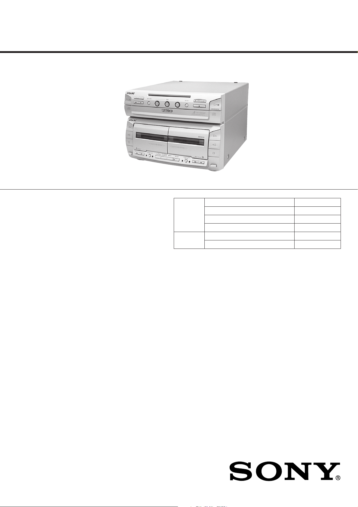
HCD-V5500
SERVICE MANUAL
Ver 1.1 2001. 11
• HCD-V5500 is the deck, CD section
in MHC-V5500/V7700AV.
Manufactured under license from Dolby Laboratories
Licensing Corporation.
“DOLBY” and the double-D symbol a are trademarks
of Dolby Laboratories Licensing Corporation.
CD CD Mechanism Type CDM38-5BD21
Section Base Unit Name BU-5BD21
Tape deck Model Name Using Similar Mechanism HCD-V8800
Section Tape Transport Mechanism Type TCM-220WR2E
E Model
Chinese Model
Model Name Using Similar Mechanism HCD-V8800
Optical Pick-up Type KSS-213B/S-N
VIDEO CD/CD player section
System Compact disc and digital
audio system
Laser Semiconductor laser
(λ=780nm)
Emission duration:
continuous
Laser output Max.44.6 µW*
*This output is the value
measured at a distance of
200 mm from the
objective lens surface on
the Optical Pick-up Block
with 7 mm aperture.
Audio
Frequency response 2 Hz - 20 kHz(±0.5 dB)
Wavelength 780 - 790 nm
Signal-to-noise ratio More than 90 dB
Dynamic range More than 90 dB
Video
Color system format NTSC, PAL
SPECIFICATIONS
CD OPTICAL DIGITAL OUT
(Square optical connector jack, rear panel)
Wavelength 600 nm
Output Level –18 dBm
Tape player section
Recording system 4-track 2-channel stereo
Frequency response 60 - 13,000 Hz (±3 dB),
(DOLBY NR OFF) using
Sony TYPE I cassette
60 - 14,000 Hz (±3 dB),
using Sony TYPE II
cassette
Design and specifications are subject to change
without notice.
9-920-958-12
2001K1600-1
© 2001.11
STEREO CASSETTE DECK CD PLAYER
Sony Corporation
Home Audio Company
Published by Sony Engineering Corporation

TABLE OF CONTENTS
1. SERVICING NOTE
······················································ 3
2. GENERAL ······································································ 4
3. DISASSEMBLY
3-1. Back Panel, CD Block Removal········································· 5
3-2. Cassette Lid (A)/(B) Assy, Mechanism Deck Removal ···· 5
3-3. Main Board, Resistor Board, Video Board,
Video In Board, Front Panel Assy Removal·······················6
4. TEST MODE ·································································· 7
5. ADJUSTMENTS
5-1. Mechanical Adjustment ······················································ 8
5-2. Electrical Adjustment ························································· 8
6. DIAGRAMS
6-1. Block Diagram — CD Section — ···································· 13
6-2. Block Diagram — Video Section — ································ 15
6-3. Block Diagram — Deck/System Control Section — ······· 17
6-4. Circuit Boards Location ··················································· 19
6-5. Schematic Diagram — Audio Section —························· 20
6-6. Printed Wiring Board — Audio Section —······················23
6-7. Printed Wiring Board — Video Section — ······················ 26
6-8. Schematic Diagram — Video Section — ························· 29
6-9. Schematic Diagram — Main Section — ·························· 33
6-10. Printed Wiring Board — Main Section — ······················· 37
6-11. Printed Wiring Board — CD Panel Section — ················ 40
6-12. Schematic Diagram — CD Panel Section — ··················· 43
6-13. Printed Wiring Board — BD Section — ·························· 45
6-14. Schematic Diagram — BD Section —·····························47
6-15. Schematic Diagram — Motor Section — ························ 49
6-16. Printed Wiring Board — Motor Section —······················51
6-17. IC Block Diagrams ··························································· 53
6-18. IC Pin Functions ······························································· 57
7. EXPLODED VIEWS
7-1. MAIN SECTION ····························································· 69
7-2. FRONT PANEL SECTION··············································70
7-3. CD MECHANISM DECK SECTION
(CDM38-5BD21) ····························································· 71
7-4. CD MECHANISM DECK SECTION-2
(CDM38-5BD21) ····························································· 72
7-5. BASE UNIT SECTION (BU-5BD21) ····························· 73
7-6. TAPE MECHANISM DECK SECTION-1
(TCM-220WR2E) ···························································· 74
7-7. TAPE MECHANISM DECK SECTION-2
(TCM-220WR2E) ···························································· 75
8. ELECTRICAL PARTS LIST ··································· 76
— 2 —
SECTION 1
H
VIDEO board
TP709 (LED)
Oscilloscope
+
_
SERVICING NOTE
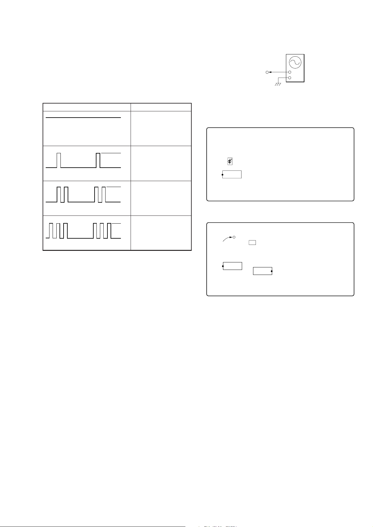
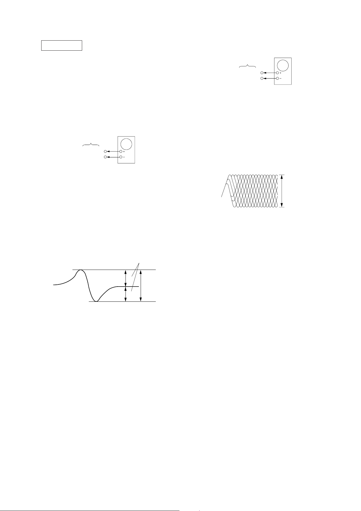
SELF-DIAGNOSIS
This model has the self-diagnosis function for the VIDEO and
AUDIO decoder sections.
Immediately after the power on, the self-diagnosis function searches
each operation of IC’s around the mechanism control microcomputer
(IC701).
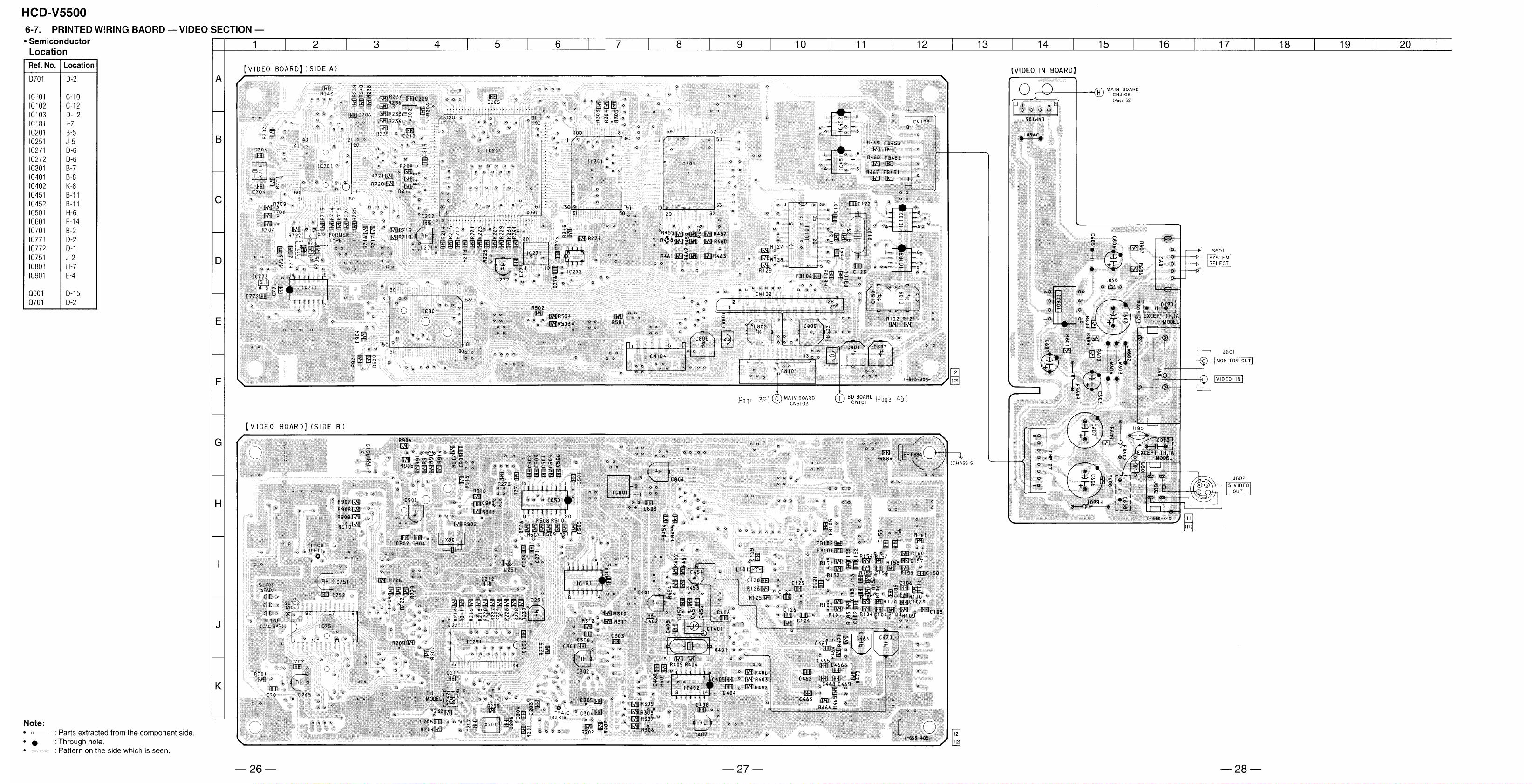
The results can be checked by connecting an oscilloscope to TP709
(LED) of the VIDEO board.
Oscilloscope (Waveform) Symptom
H
No error
L
Light
Note: The LED for check (D701) is mounted to some sets
(FORMER TYPE). In this case, confirm the lighting
condition of LED.
[VIDEO BOARD] (SIDE A)
1 time blinking
2 time blinking
3 time blinking
H
External SRAM (IC751)
L
error
H
MPEG decoder (IC201)
L
error
DRAM (IC251)
error
L
D701
IC771
[VIDEO BOARD] (SIDE B)
TP709 (LED)
IC751
X901
IC251
— 3 —
SECTION 2
GENERAL
@ª
@•
@¶
3
12 5 7 8 9 !¡
@§
4
@∞
6
@¢
@£
@™
@¡
@º
!º
!ª
!¶
!•
!™
!£
!¢
!∞
!§
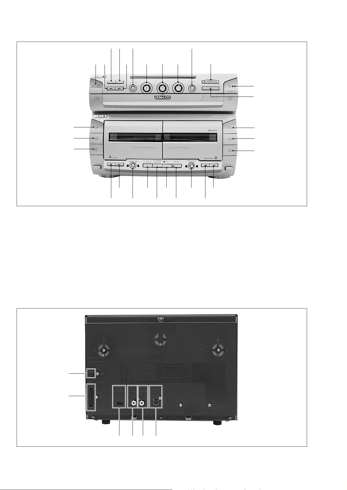
1 DISC SKIP EX-CHANGE Button
(CD)
2 0 Button (CD)
3 PREV Button (CD)
4 NEXT Button (CD)
5 ) Button (CD)
6 RETURN Button (CD)
7 DISC 1 Button (CD)
8 DISC 2 Button (CD)
9 DISC 3 Button (CD)
!º SELECT Button (CD)
#º
!¡ 6 OPEN/CLOSE Button (CD)
!™ ·P CD NON-STOP Button (CD)
!£ p Button (CD)
!¢ · Button [B] (DECK)
!∞ ª Button [B] (DECK)
!§ π Button [B] (DECK)
!¶ ) Button [B] (DECK)
!• 0 Button [B] (DECK)
!ª DIRECTION MODE Button
(DECK)
@º PAUSE Button (DECK)
@¡ REC Button (DECK)
@™ HI-SPEED DUBBING Button
(DECK)
@£ CD SYNCHRO Button (DECK)
@¢ DOLBY NR Button (DECK)
@∞ ) Button [A] (DECK)
@§ 0 Button [A] (DECK)
@¶ π Button [A] (DECK)
@• ª Button [A] (DECK)
@ª · Button [A] (DECK)
#¡
#º OPTICAL DIGITAL OUT
#¡ SYSTEM CONTROL CONNECTOR
#™ SYSTEM SELECT SWITCH
#™ #£
#¢ #∞
#£ VIDEO IN JACK
#¢ MONITOR OUT JACK
#∞ S VIDEO JACK
— 4 —
SECTION 3
0
DISASSEMBLY
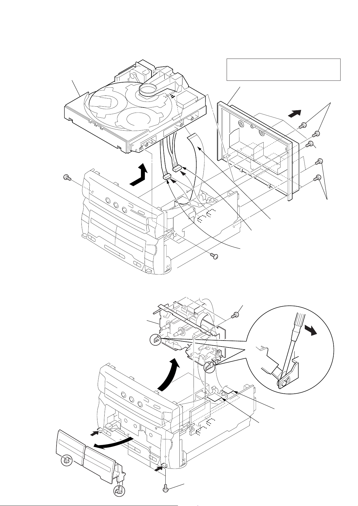
Note : Follow the disassembly procedure in the numerical order given.
3-1. BACK PANEL, CD BLOCK REMOVAL
9
CD block
8
Screw
+BVTP 3
×
10
CASE
Unscrew the fi ve case attachment in the screws (case)
(M3 × 8) × 4, (+BV 3 × 8) × 1 and remove the case.
3
Back panel
1
Screw
+BVTP 3
2
Screw
+BVTP 3
×
1
×
8
7
Screw
+BVTP 3
3-2. CASSETTE LID (A)/(B) ASSY, MECHANISM DECK REMOVAL
1
Press the EJECT button and open the cassette lid.
Mechanism Deck (TCM-220WR2E)
7
+BVTP 2.6
6
Screw
4
5
CN112 (9 pin)
CN111 (8 pin)
×
10
×
8
1
Screw
+BVTP 3
Flat wire (19 core)
2
×
10
1
3
1
8
6
Screw
+BVTT 3
— 5 —
4
Flat wire (11 core)
5
Flat wire (21 core)
×
8
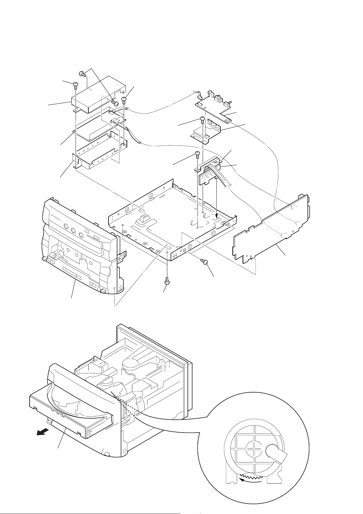
3-3. MAIN BOARD, RESISTOR BOARD, VIDEO BOARD, VIDEO IN BOARD,
d
FRONT PANEL ASSY REMOVAL
6
3
Screw
+BVTP 3
7
Bracket V (T)
9
VIDEO board
7
Bracket V (B)
×
10
Screw
+BVTP 3
×
10
8
Screw
+BVTP 3
5
!£
+BVTP 3
×
8
!º
Screw
+BVTP 3
Screw
4
×
8
×
8
!¡
VIDEO IN board
!™
Bracket (BP)
!¢
Bracket (H/S)
!∞
Resistor board
1
2
Front panel assy
Screw
+BVTP 3
×
8
• Tray (Slide) getting out procedure on the power supply is OFF
Rotate the BU CAM assembly in the direction of the arrow and pull out the slide.
!§
Screw
+BVTP 3
!¶
Main boar
×
8
Tray (Slide)
1
BU CAM assy
— 6 —

SECTION 4
TEST MODE
VIDEO CD COLOR-BARS MODE
On this mode, the data of the color-bars signal as a picture signal
and the 1kHz sine wave signal as a sound signal are output by the
mechanism control microcomputer (IC701) for video CD signal
check. When measurement of the voltage and waveform on the
VIDEO board, perform it in this mode.
For reference, the color-bars signal can be observed at J9001
(VIDEO OUT) and the sound signal can be observed at J101
(VIDEO (AUDIO) OUT) using an oscilloscope.
1. Connect the lead wire to both ends of the land of SL701 (CAL
BAR) of the VIDEO board.
2. Turn the power on. Press FUNCTION button to select CD.
3. After 2 or 3 seconds later, connect the lead wire.
4. After measuring, remove the lead wire connected.
Note : The 1kHz sine wave is not outputted when the CD is played
once, but it is not error.
[VIDEO BARD ] (SIDE B)
SL703 (AFADJ)
SL702 (ADJ)
IC751
IC251
SL701 (CAL BAR)
— 7 —
SECTION 5
ADJUSTMENTS
5-1. MECHANICAL ADJUSTMENT
PRECAUTION
1. Clean the following parts with a denatured-alcohol-moistened
swab:
record/playback head pinch roller
erase head rubber belts
capstan idlers
2. Demagnetize the record/playback head with a head
demagnetizer.
3. Do not use a magnetized screwdriver for the adjustments.
4. After the adjustments, apply suitable locking compound to the
parts adjusted.
5. The adjustments should be performed with the rated power
supply voltage unless otherwise noted.
• T orque Measurement
Mode Torque Meter Meter Reading
Forward CQ-102C
Forward
Back Tension (0.028 – 0.083 oz•inch)
Reverse CQ-102RC
Reverse
Back Tension (0.028 – 0.083 oz•inch)
FF, REW CQ-201B
CQ-102C
CQ-102RC
36 to 61g•cm
(0.50 – 0.84 oz•inch)
2 to 6g•cm
36 to 61g•cm
(0.50 – 0.84 oz•inch)
2 to 6g•cm
61 to 143g•cm
(0.85 – 1.99 oz•inch)
5-2. ELECTRICAL ADJUSTMENT
DECK SECTION
1. The adjustment should be performed in the publication.
(Be sure to make playback adjustment at first.)
2. The adjustment and measurement should be performed for both
L-CH and R-CH.
• Switch position
DOLBY NR switch : OFF
FUNCTION button : OFF
EFFECT switch : OFF
DBFB switch : OFF
3. Deck section electrical adjustments are made in test mode by
press key switch same time CD STOP DECK A ST OP and
DECK B STOP button.
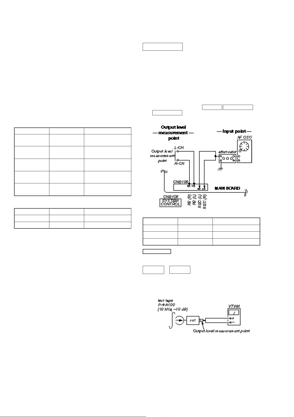
4. Input point and output level measurement point.
• T ape Tension Measurement
Mode Tension Meter Meter Reading
Forward CQ-403A
Reverse CQ-403R
more than 100 g (3.53 oz)
more than 100 g (3.53 oz)
• Test Tape
Tape Signal Used for
P-4-A100 10 kHz, –10 dB
P-4-L300 315 Hz, 0dB Level Adjustment
WS-48B 3 kHz, 0dB Tape Speed Adjustment
0 dB=0.775V
Record/Playback Head Azimuth Adjustment
DECK A DECK B
Procedure:
1. Forward Playback mode
Reverse Playback mode
Head Azimuth Adjustment
— 8 —
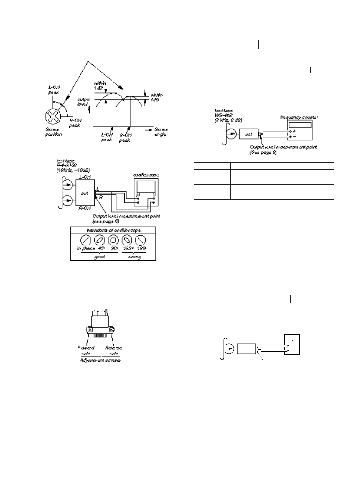
2. Turn the adjustment screw for the maximum output levels. If
t
these levels do not match, turn the adjustment screw until both
of output levels match together within 1 dB.
3. Playback Mode
Tape Speed Adjustment DECK A DECK B
Note: Start the Tape Speed adjustment as below after setting to the
test mode.
Set to test mode. (Press key switch same time CD STOP
DECK A STOP and DECK B STOP button.)
Test mode off. (Power off.)
Procedure:
• Perform high speed adjustment before normal speed adjustment.
Mode: Playback
4. Change the playback mode and repeat the steps 1 to 3.
5. After the adjustment, lock the adjustment screw with suitable
locking compound.
Adjustment Location:
— Record/playback head (Deck A and B) —
Speed
*High
Normal
Deck
A
B
A
B
Adjustment
RV652
RV652
RV651
RV651
Frequency counter
5,910 to 6,090 Hz
2,910 to 3,090 Hz
* Continue to press HIGH SPEED DUBBING switch (S259) in
playback mode : High speed playback.
Frequency difference between the beginning and the end of the
tape should be within ± 3%.
Frequency difference between deck A and deck B the beginning
of the tape should be within 1.5 %.
Adjustment Location: AUDIO board (See page 10)
Sample Value of Wow and flutter
W.RMS (JIS) within 0.3%
(test tape: WS-48B)
Playback level Adjustment DECK A DECK B
Procedure:
— FWD playback Mode —
test tape
P-4-L300
(315 Hz, 0 dB)
VTVM
set
Output level measurement poin
(See page 8)
+
–
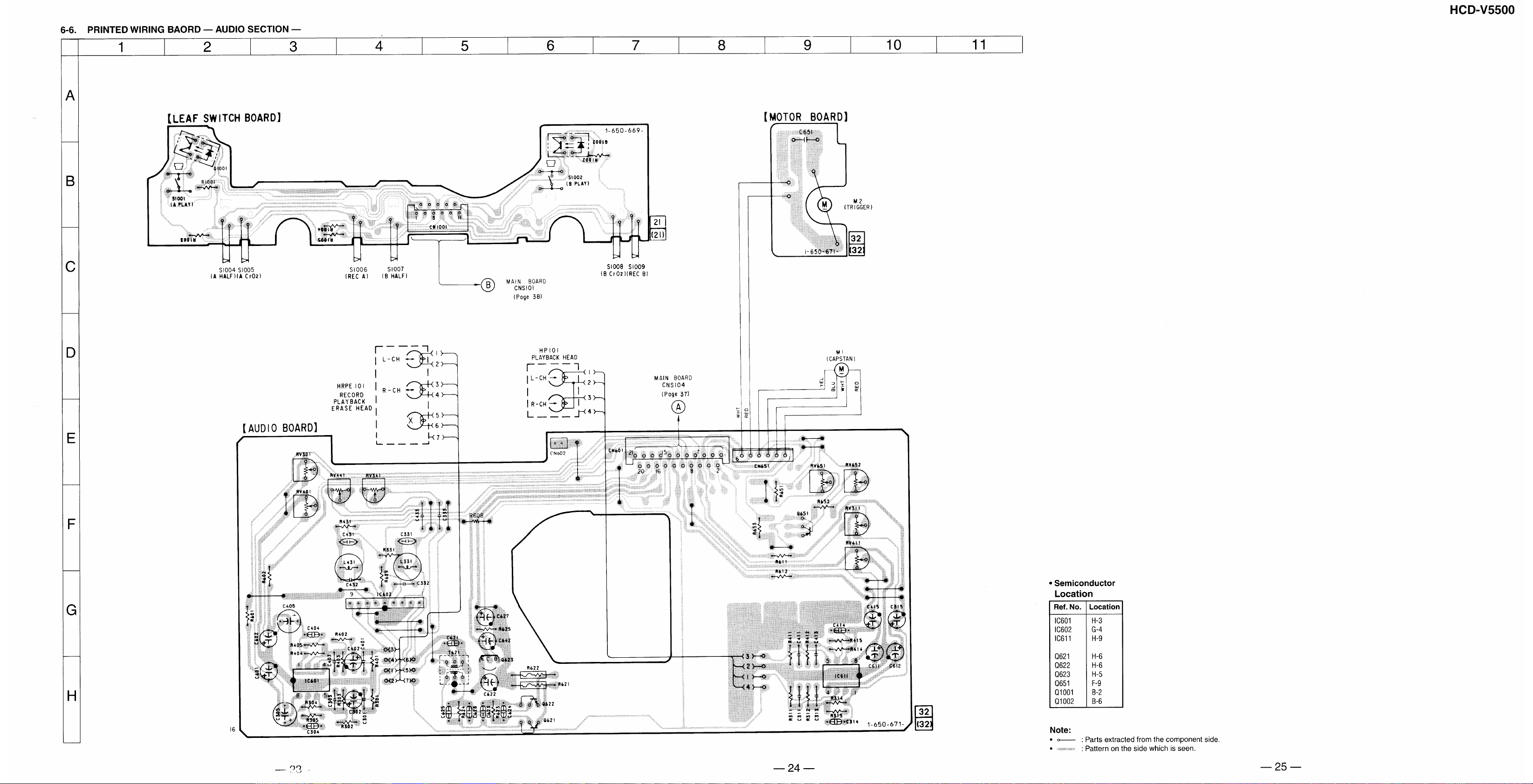
Deck A is RV311 (L-CH) and RV411 (R-CH), Deck B is RV301
(L-CH) and RV401 (R-CH) so that adjustment within adjustment
level as follows.
Adjustment Level:
LINE OUT level : –8.2 to –7.2 dB (301.5 to 338.3 mV)
Level Difference between Channels : within 0.5 dB
Confirm the OUTPUT level does not change in playback mode
while changing the mode from playback to stop several times.
Adjustment Location: AUDIO board (See page 10)
— 9 —
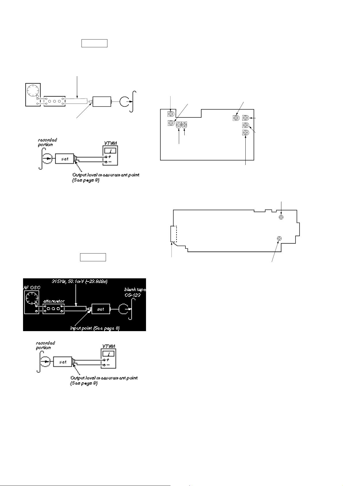
Record Bias Adjustment DECK B
)
Procedure:
1. Record mode
1) 315 Hz
2) 10 kHz
AF OSC
attenuator
50.1mV (–23.8dBs)
set
blank tape
CS-123
Adjustment Level:
OUTPUT level: –23.8 dB ± 1.0 dB (56.1 to 44.6 mV)
Adjustment Location: MAIN board
Adjustment Location :
[AUDIO BOARD] — Component Side —
RV301 : Playback Level (Deck B L-CH)
RV401 : Palyback Level
(Deck B R-CH)
RV651 : Tape Speed (Normal)
Input point (See page 8)
2. Mode: Playback
3. Confirm playback the signal recorded in step 1 become
adjustment level as follows.
4. If these levels do not adjustment level, adjustment the RV341
(L-CH) and RV441 (R-CH) to repeat steps 1 and 4.
Adjustment level: Playback output of 315 Hz to playback output
of 10 kHz: 0 ± 1.0 dB (0 ± 4.5mV).
Adjustment Location: AUDIO board
Record Level Adjustment DECK B
Procedure:
1. Record mode
RV341 : Record Bias (L-CH)
RV441 : Record Bias (R-CH)
RV411 : Playback Level (Deck A R-CH)
[MAIN BOARD] — Component Side —
RV451 Record Level (R
CNB108
RV401 Record Level (L)
RV652 : Tape Speed
(Hight)
RV311 : Playback Level
(Deck A L-CH)
2. Playback mode
3. Confirm playback the signal recorded in step 1 become
adjustment level as follows.
4. If these levels do not adjustment level, adjustment the RV401
(L-CH) and RV451 (R-CH) to repeat steps 1 and 4.
— 10 —
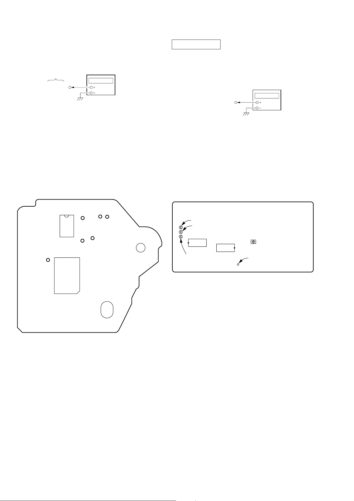
CD SECTION
BD board
Oscilloscope
TP (RF)
TP (VC)
Note :
1. CD Block is basically designed to operate without adjustment.
Therefore, check each item in order given.
2. Use YEDS-18 disc (3-702-101-01) unless otherwise indicated.
3. Use an oscilloscope with more than 10MΩ impedance.
4. Clean the object lens by an applicator with neutral detergent
when the signal level is low than specified value with the
following checks.
S Curve Check
Oscilloscope
BD board
TP (FE)
TP (VC)
RF Level Check
Procedure :
1. Connect oscilloscope to test point TP (RF) on BD board.
2. Turned Power switch on.
3. Put disc (YEDS-18) in to play the number five track.
4. Confirm that oscilloscope waveform is clear and check RF
signal level is correct or not.
Note : A clear RF signal waveform means that the shape “◊” can
be clearly distinguished at the center of the waveform.
RF signal waveform
Procedure :
1. Connect oscilloscope to test point TP (FE) on BD board.
2. Connect between test point TP (FEI) and TP (VC) by lead wire.
3. Turned Power switch on.
4. Put disc (YEDS-18) in and turned Power switch on again and
actuate the focus search. (actuate the focus search when disc
table is moving in and out.)
5. Check the oscilloscope waveform (S-curve) is symmetrical
between A and B. And confirm peak to peak level within 3 ± 1
Vp-p.
S-curve waveform
Symmetry
A
Within 3
B
±
1 Vp-p
6. After check, remove the lead wire connected in step 2.
Note : • Try to measure several times to make sure than the ratio
of A : B or B : A is more than 10 : 7.
• Take sweep time as long as possible and light up the
brightness to obtain best waveform.
VOLT/DIV : 200mV
TIME/DIV : 500ns
Level : 1.3 Vp-p
+0.25
–0.20
— 11 —
RF PLL Free-run Frequency Check
r
r
Procedure :
1. Connect frequency counter to TP (PLCK) with lead wire.
VIDEO SECTION
Frequency adjustment
BD baord
TP (PLCK)
frequency counte
2. Turned Power switch on.
3. Put the disc (YEDS-18) in to play the number five track.Conf irm
that reading on frequency counter is 4.3218 MHz.
Adjustment Location :
[BD BOARD] — SIDE A —
(FEI)
(FE)
(TE)
(PLCK)
IC103
(RF)
(VC)
1. Connect the frequency counter to check point of the VIDEO
board.
frequency counte
VIDEO board
TP410 (DCLK)
2. Adjust CT401 of the VIDEO board so that the frequency counter
read 13.5 MHz ± 40 Hz at STOP condition.
[VIDEO BOARD] — SIDE B —
SL703 (AFADJ)
SL702 (ADJ)
IC751
IC251
SL701 (CAL BAR)
CT401
Frequency
TP410 (DCLK)
IC101
— 12 —
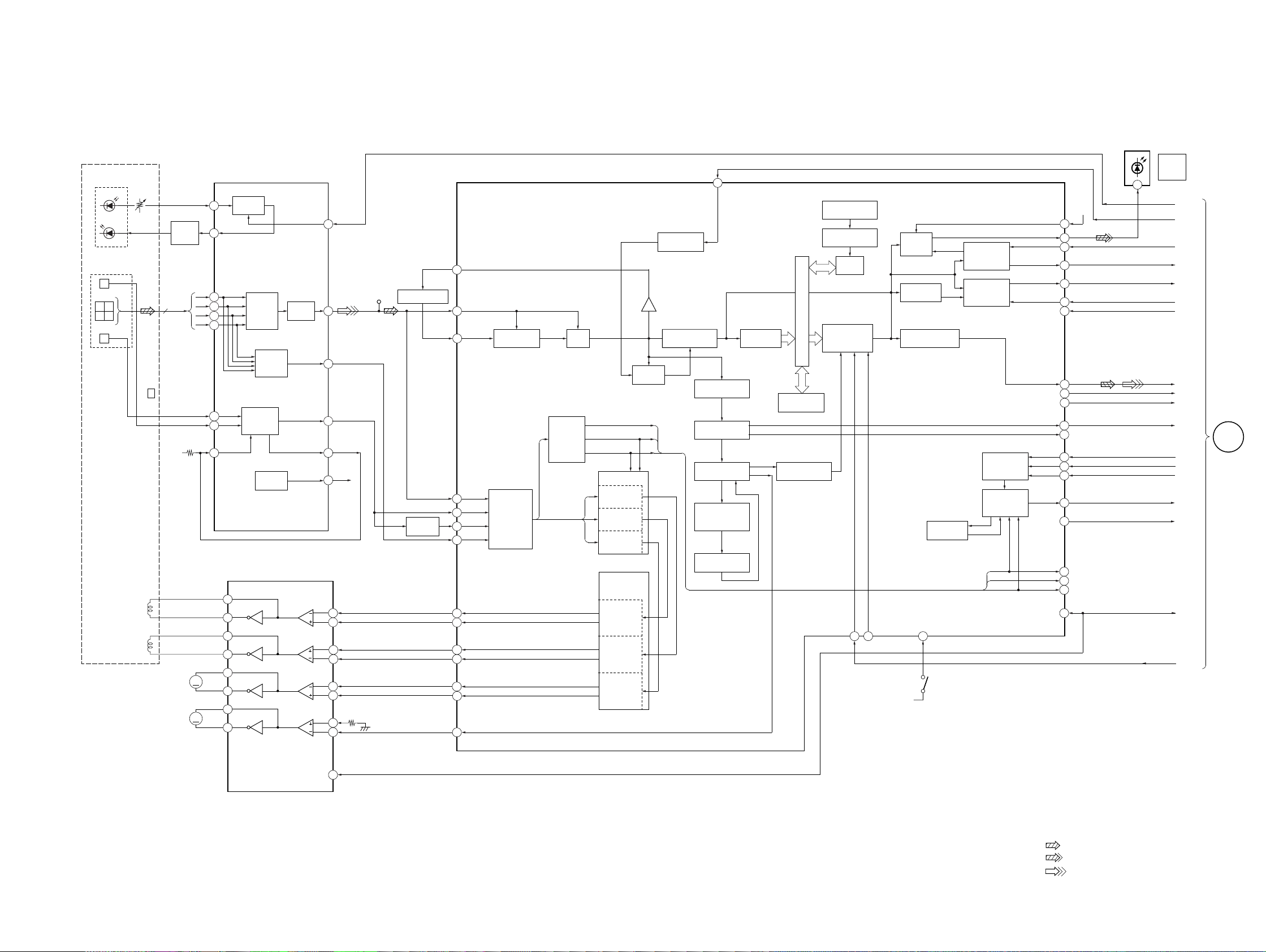
6-1. BLOCK DIAGRAM — CD SECTION —
HCD-V5500
SECTION 6
DIAGRAMS
OPTICAL PICK-UP
BLOCK (KSS-213B/S-N)
LASER
DIODE
PD
DETECTOR
E
AC
BD
F
LD
TRACKING
COIL
FOCUS
COIL
LD
POWER
1
4
M102
SLED
MOTOR
M101
SPINDLE
MOTOR
LD
DRIVE
Q101
VC
IC107
RF AMP
IC103
APC LD
2
AMP
RF FQ
AMP
19
RF
INTEGRATOR
16
15
13
1110
VC
12
INTE-
GRATOR
4
5
19
20
10
9
23
24
1
3
4
5
6
8
9
T+
T–
F+
16
F–
17
13
M
12
27
M
26
RF
SUMMING
AMP
FOCUS
ERROR
AMP
TRACKING
ERROR
AMP
VC
BUFFER
FOCUS/TRACKING COIL DRIVE
SPINDLE/SLED MOTOR DRIVE
IC102
1
2
DIGITAL SERVO
DIGITAL SIGNAL PROCESSOR
IC101
ASY0
39
RF AC
36
ASY1
38
RF DC
26
TE
27
SE
28
FE
29
TFDR
4
TRDR
6
FFDR
8
FRDR
10
SRDR
2
SFDR
100
MDP
96
ASYMMETRY
CORRECTION
A/D
CONVERTER
MIRR
DFCT
FOK
DETECTOR
MIX
FOK
DFCT
MIRR
SERVO DSP
FOCUS
SERVO
TRACKING
SERVO
SLED
SERVO
PWM
GENERATOR
TRACKING
PWM
GENERATOR
FOCUS
PWM
GENERATOR
SLED
PWM
GENERATOR
DIGITAL
PLL
CLOCK
GENERATOR
EFM
DEMODULATOR
62
XTAL
SYNC
PROTECTOR
TIMING
GENERATOR 1
CLV SERVO
PROCESSOR
1B TIMS
OVERSAMPLING
FILTER
NOISE
SHAPER
REGISTER
DATA BUS
ERROR
CORRECTOR
TIMING
GENERATOR 2
PRIORITY
EMCODER
ADDRESS
GENERATOR
32K
RAM
D/A
DATA
PROCESSOR
MUTE
79 54
GFS
DIGITAL
OUT
PEAK
DETECTOR
SERIAL/PARALLEL
PROCESSOR
INTERFACE
S STOP
99
SWITCH
+5V
SERVO
S101
LIMIT
SUBCODE
P-W
PROCESSOR
SUBCODE
Q
PROCESSOR
INTERFACE
SEQUENCER
CPU
SERVO
AUTO
MD2
DOUT
EXCK
SBSO
SUBQ
SQCK
SCLK
DATA
LRCK
BCLK
SCOR
WFCK
DATA
XLT
CLK
SENS
C2PO
FOK
DFCT
MIRR
XRST
+5V
70
71
76
75
77
78
83
46
45
47
74
73
86
87
88
80
56
93
92
91
81
DIGITAL
OUT
OPTICAL
1
LDON
384BD
EXCK
SUBQ
SUBQ
SQCK
SCLK
ADATA
LRCK
BCLK
SCOR
B
DATA
XLT
CLK
SENS
C2PO
XRST
AMUTE
VIDEO
SECTION
(Page 15 )
15MUTE
16
• SIGNAL PATH
: CD
: DIGITAL OUT
: VIDEO
— 13 — — 14 —
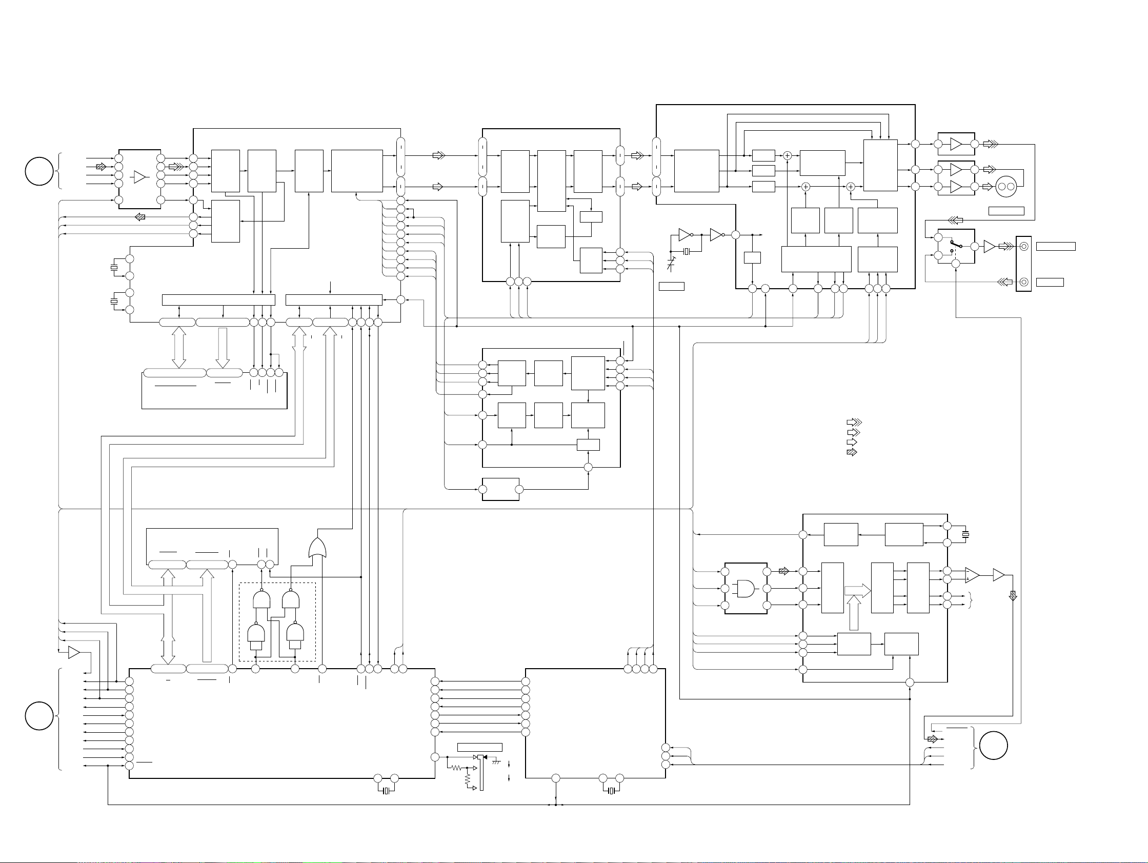
HCD-V5500
6-2. BLOCK DIAGRAM — VIDEO SECTION —
10BIT VIDEO D/A CONVERTER
IC401
B
CD
SECTION
(Page 14 )
IC501
(2/2)
B
CD
SECTION
(Page 14 )
16
BCK
ADATA
LRCK
C2PO
384FS
ADATA
LRCK
BCLK
28.63636MHz
45.1584MHz
DATA
CLK
AMUTE
384FS
416
384FS
DATA
CLK
AMUTE
SQCK
SUBQ
SCLK
XLT
LDON
SCOR
SENS
XRST
X202
X201
IC501 (1/2)
9
8
7
6
5
106
107
73
78
74
11
10
77
76
75
71
62
48
BUFFER
XTL0O
2
XTL01
3
XTL2O
XTL2I
DATA
CLK
AMUTE
SQCK
SUBQ
SCLK
XLT
LDON
SCOR
SENS
RESET
38–43 46–55•
•
•11–13 15–19
D0
112
111
110
109
103
100
101
102
D-RAM INTERFACE
•
A0
I/O8
2–10 21 23–25
21–29 • 31–3513 – 20
A0
D7
11
12
13
14
15
2–5 7–10 35–38 40–43
•
DQ1
I/O1
CD-ROM
DECODER
MPEG
AUDIO
DECODER
17–21 23 24 32 33••••
18–21 24–28•
A8
A0
DQ16
D-RAM
IC251
S-RAM
IC751
A12
A12
OE
55
RD
••
MPEG DECODER
IC201
VIDEO
POSTPROCESSOR
SYNC GENERATOR
A0
A3
XHCS
XTCS
AS
&
117115116114
XWR
XHDT
WR
WAIT
DECODER
7–13 16
LCAS
UCAS
IC772
WE
6
54
3
12
40
A17
IC701
MPEG
VIDEO
EACH CIRCUIT BLOCK
HOST INTERFACE
5 6•• •119 120
•
D0
D7
IC771
MPEG
SYSTEM
DECODER
34
3735
301516 31
W
RAS
CE1
272022
8
10 9
11
12
13
41 54 56 43 70 7 8
A18
MECHA CONTROL
XHIRQ
XHIRQ
EXTAL
Y
C
118
VDAC-XLAT
XTAL
5251
71
74
•
76
80
63
70
97
95
92
93
94
89
56
57
58
59
XRST
GENERATOR
DF-XLAT
X701
10MHz
XSGRST
HSYNC
VSYNC
FID
DCLK
XOSDEN
OSD B
OSD G
OSD R
CLOCK
IC272
CMD0
CMD1
CMD2
CMD3
SACK
QINT
MREQ
NPIN
Y0-Y7
C0-C7
1
2
3
4
5
6
72
64
OSD B
OSD G
OSD R
XOSDEN
VSYNC
HSYNC
DCLK
SYSTEM SELECT
1
4
Y
•
6
9
11
C
18
18
17
16
15
19
20
CK 1/2 Q
1 5
S601
RGB-YUV
CONV.
TIMING
GEN.
98 10097
HSYNC
OUTPUT
CONT.
SYNC
CONT.
PAL
AUTO
NTSC
NOISE REDUCTION
REDUSER
MEMORY
DCLKI
VSYNC
DCLK
VIDEO
RAM
DATA
SEL.
34
CMD0
35
CMD1
36
CMD2
37
CMD3
44
SACK
18
QINT
MREQ
43
IC301
NOISE
CONT.
OSD
IC271
6.75MHz
CD-XRST
YUV-RGB
CONV.
DRAM
IF
DATA INPUT
SHIFT
RESISTOR
DISPLAY
POSITION
CONT.
OSC
8
IIC INTERFACE
IC901
VIDEO AMP
IC451
&
INTER-
49 504859 60625557 51
CLK
V
Y
C
VDAC-XLAT
24
29325
5 7
3
Y/C AMP
IC452
1
3
2
SELECTOR
7
1
7
IC601
4
3
J603
S VIDEO OUT
Q601
J601
MONITOR OUT
VIDEO IN
60
67
51
58
29
30
31
4
3
2
1
NR-XCS
MCLK
MDATA
RESET
MDATA
OS-XLAT
MCLK
1
4
•
6
9
11
18
CT401
13.5MHZ
DEMPX, LEVEL
TRANSLATOR
&
INTERPOLTATOR
CLOCK GENARATOR
IC402
56
4
3
X401
27MHz
HSYNC
Y, C/Y, U, V
SELECTOR
POLATOR
CLOSED
CAPTION
ENCODER
SIO & I2O-BUS
CONT.
DATA
LPF
LPF
DELAY
56
1/2
XRST
DCLK
MODULATOR
SYNC
SLOPE
GEN.
SYNC GEN.
TIMING CONT.
XVRST
SUB
CARRIER
GEN.
&
FID
VSYNC
• R CH: Same as L ch
• SIGNAL PATH
: VIDEO
: Y
: CHROMA
: CD
DIGITAL FILTER & D/A CONVERTER
384FS
BUFFER
ADATA
LRCK
BCLK
DATA
CLK
DF-XLAT
68494847
MCLK
MDATA
NR-XCS
OS-XLAT
15
RESET
55
IIC-DATA
56
X2
IIC-CLK
X1
111052
X901
5MHz
AMUTE
XRST
IC181
13
4
1
11
6
3
11
12
10
TIMING
6
CIRCUIT
INPUT PLM
3
4
5
2
MODE
IC101
D/A
CONV.
CLOCK
GENERATOR
MUTE
CIRCUIT
INT
1
21
22
27
25
16
18
CD FUNC
L CH
XRST
IIC-DATA
IIC-CLK
ACTIVE LPF
2
3
X101
33.8688MHz
IC102
16 7
R CH
A
MAIN
SECTION
(Page 17)
— 15 — — 16 —
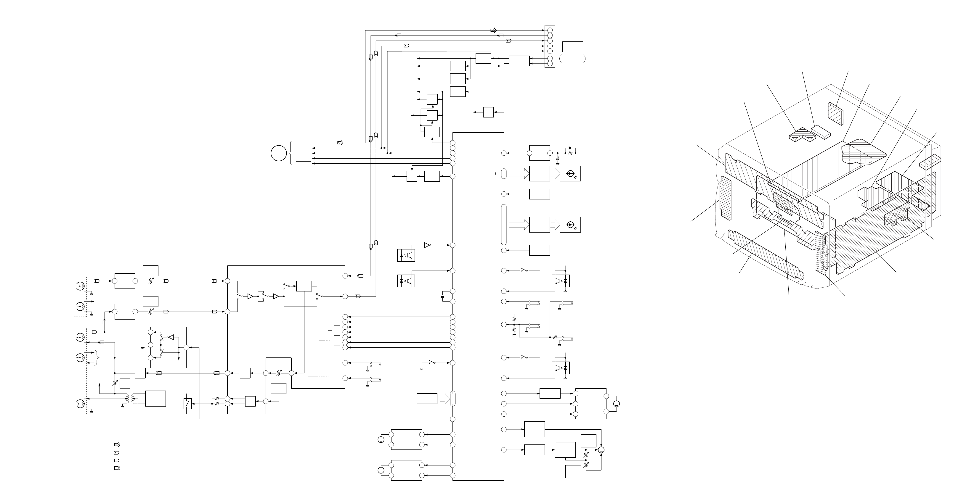
6-3. BLOCK DIAGRAM — DECK/SYSTEM CONTROL SECTION — 6-4. CIRCUIT BOARDS LOCATION
(B)
A +7.5V
D +5V
+12V
+7V
+5V
A +5V
Q104
Q102
REG
IC853
REG
Q852
REG
IC852
-7.5V
REG
IC851
-REG
Q855
RECT
Q901-904
CD L
REC L
PB L
IIC DATA
IIC CLK
2
6
CNB108
7
12
14
AC
11
AC
15
SYSTEM
CONTROL1
TO STR-W550
CNP701
CONNECTOR BOARD
SENSOR BOARD
MOTOR BOARD
HCD-V5500
MOTOR (TURN) BOARD
VIDEO BOARD
BD BOARD
MOTOR (SLIDE) BOARD
REC/PB
HEAD
(A DECK)
REC/PB
HEAD
(B DECK)
ERASE
HEAD
16
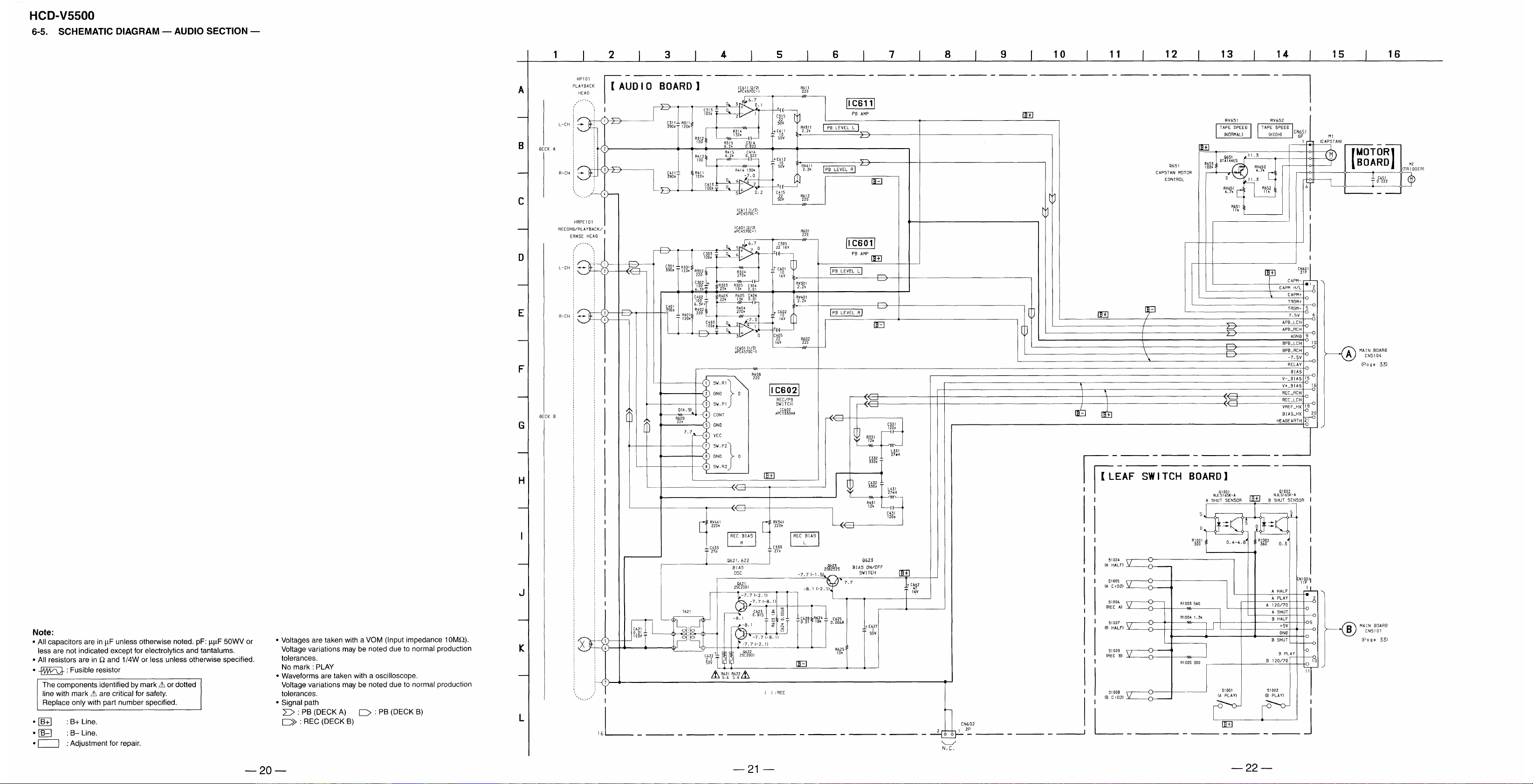
HP101
HRPE101
R CH
R CH
R CH
3
5
RV341
Signal path
PB EQ
AMP
IC611
PB EQ
AMP
IC601
1
7
C331,L331
BIAS
TRAP
REC
BIAS
: CD
: PB(DECK A)
: PB(DECK B)
: REC(DECK B)
RV311
PB(L)
LEVEL
RV301
PB(L)
LEVEL
REC/PB SWITCH
1
2
3
BIAS
OSC
Q621,622
IC602
R CH
Q623
4
+7.5V
(Page 16 )
IC401
DOLBY NR/REC EQ AMP
2
A
B
4
REC
11
EQ
NORM
29
28
CROM
BIAS
SW
VIDEO
SECTION
70
120
A
REC
PB
10
RV401
REC(L)
LEVEL
22 A7.5V
IIC DATA
IIC CLK
CD FUNC
DOLBY
9
L CH
XRST
B
DOL
PAS
NORM/HIGH
BIAS ON/OFF
RM ON/OFF
NR ON/OFF
REC PB/PASS
LM ON/OFF
NORM/CROM/METAL
REC
PB
PB A/B
A120/70
SWITCH
Q103
46
55
56
57
37
IN2
IN1
R IN
F IN
SWITCH
Q106
Q701
5MHz
S801
OPEN SW
S851
ROTARY
ENCODER
6
3
2
10
X101
37
75
76
11
10
87
88
89
90
91
92
93
81
80
.
79
.
78
96
61
60
64
63
D +5V
IC703
DISC
SENSOR
6
8
12
14
16
17
18
19
20
13
15
MOTOR
MOTOR
M701
TURN
M801
SLIDE
IC702
TABLE
SENSOR
S1005
A CrO2
DET
S1008
B CrO2
DET
M
M
2
7
4
7
Q105
IC701
MOTOR DRIVE
OUT2
OUT1
IC801
MOTOR DRIVE
OUT2
OUT1
IC101
SYSTEM CONTROL
CD POWER
IIC DATA
IIC CLK
XRST
CD FUNC
DISC SENS
TBL SENS
X1
X2
PB A/B
EQ H/N
BIAS
REC MUTE
NR ON/OFF
R/P PASS
LM ON/OFF
OUT OPEN
E1
E2
E3
TC RELAY
TBL R
TBL L
LOAD IN
LOAD OUT
CAP M ON/OFF
RESET
LED1
LED6
KEY A
LED7
LED20
KEY B
A PLAY SW
A SHUT
A HALF SW
B HALF SW
B PLAY SW
B SHUT
TRG LOW
B TRG
A TRG
CAP M H/L
VIDEO IN BOARD
CD PANEL BOARD
RESET
+5V
S1001
A PLAY
S1002
B PLAY
3
IC103
LED
DRIVE
Q201-204
Q219,220
S251-266
FUNCTION
KEY
LED
DRIVE
Q205-218
S270-282
FUNCTION
KEY
S1004
A HALF
S1007
B HALF
CAPSTAN
MOTOR
SWITCH
Q405,408
SWITCH
Q409
+5V
+5V
SWITCH
Q410,411
1
D201-210
D211-227
+5V
+5V
SPEED
CONTROL
Q651
15
2
7
29
73
.
72
.
70
65
.
53
49
.
41
30
94
26
97
28
95
27
85
84
83
86
82
ROTATION
ROTATION
4
6
5
RV651
TAPE
SPEED
(NOMAL)
+5V
Q1001
DET A
S1006
REC A
S1009
REC B
Q1002
DET B
IC402
TRIGGER
MOTOR DRIVE
VZ
IN2
IN1
RV652
TAPE
SPEED
(HIGH)
OUT1
OUT2
M
2
10
M1
CAPSTAN
MOTOR
M
M2
TRIGGER
MOTOR
TC (A) BOARD
LEAF SWITCH BOARD
TC PANEL BOARD
AUDIO BOARD
TC
RESISTOR BOARD
MAIN BOARD
BOARD
— 17 — — 18 — — 19 —
 Loading...