

Sony HCD-D11, HCD-T11 Service Manual
Q
Q
3
7
6
3
1
5
1
5
0
HCD-D11/T11
SERVICE MANUAL
TEL 13942296513 QQ 376315150 892498299
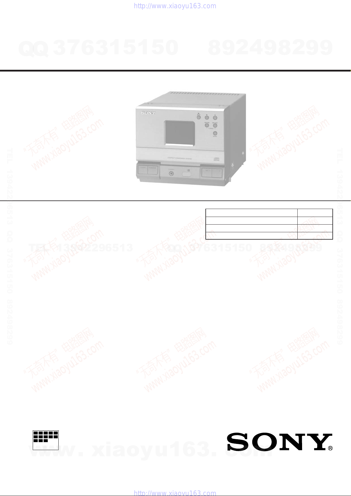
• HCD-D11/T11 is the tuner, CD player and
preamplifier section in CMT-D11/T11.
Photo: HCD-T11
4
2
9
8
Model Name Using Similar Mechanism NEW
CD Mechanism Type
Base Unit Name BU-5BD19
Optical Pick-up Name KSS-213B/K-N
9
Canadian Model
2
8
US Model
Tourist Model
E Model
HCD-D11/T11
CDM13C-5BD19
9
HCD-T11
9
TEL 13942296513 QQ 376315150 892498299
TEL
13942296513
Tuner section
Tuning range
US, Canadian model:
FM :87.5 – 108 MHz
AM:531 – 1,710 kHz (at 9 kHz interval)
530 – 1,710 kHz (at 10 kHz interval)
Except US, Canadian model:
FM :87.5 – 108 MHz
AM:531 – 1,602 kHz (at 9 kHz interval)
530 – 1,710 kHz (at 10 kHz interval)
Intermediate frequency
FM :10.7 MHz
AM: 450 kHz
Aerial terminals
FM :75 ohm unbalanced
AM:External aerial terminal
Timer Quarts lock system
Timer setting
One-minute step
Sleep timer 10-minute step, max. 90 minutes
CD player section
System Compact disc digital audio system
Laser Semiconductor laser
Wavelength 780 – 790 nm
Frequency response
2 Hz – 20 kHz ± 0.5 dB
Signal to noise ratio
More than 90 dB
Harmonic distortion
Less than 0.03%
6
7
3
Q
Q
SPECIFICATIONS
Preamplifier section
Frequency response
Inputs PC/MD IN (US, Canadian model) :
Outputs DIGITAL OUT (CD OPTICAL OUT) jack:
General
Power requirents
US, Canadian model
Except US, Canadian model
Power consumption
9
2
8
9
4
2
9
8
0
5
1
5
1
3
15 Hz – 50 kHz dB
MD IN (Except US, Canadian model) :
Stereo phone jack, sensitivity 450 mV, impedance 47 kilohms
Digital connector, –18 dBm, wavelength 660 nm
OUTPUT jack:
Stereo phones jack, 1 V, 1 kohm
PC/MD OUT jack (US, Canadian model):
MD OUT jack (Except US, Canadian model):
Stereo phone jack, 250 mV, 1 kohm
PHONES (headphones) jack:
Stereo mini jack, accepts headphones of 8 ohms or more.
120 V AC, 60 Hz
120 V or 220 – 240 V AC, adjustable, 50/60 Hz
25 W (HCD-T11)
20 W (HCD-D11)
+0
–3
– Continued on next page –
TUNER CD PLAYER
9
MICROFILM
w
w
w
.
xia
o
y
u
1
6
3
.
c
o
m
7
Q
Q
Dimensions Approx. 142 × 125 × 252 mm
Mass Approx. 3 kg (6 lb 10 oz)
Design and specifications are subject to change without notice.
TEL 13942296513 QQ 376315150 892498299
3
(w/h/d) (5
incl. projecting parts and controls
5
6
/8 × 5 × 10 inches)
3
1
5
1
5
0
1. SERVICE NOTES
2. GENERAL
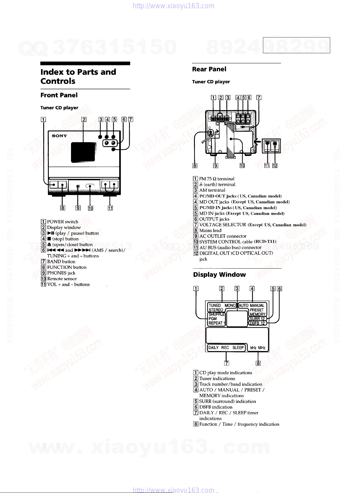
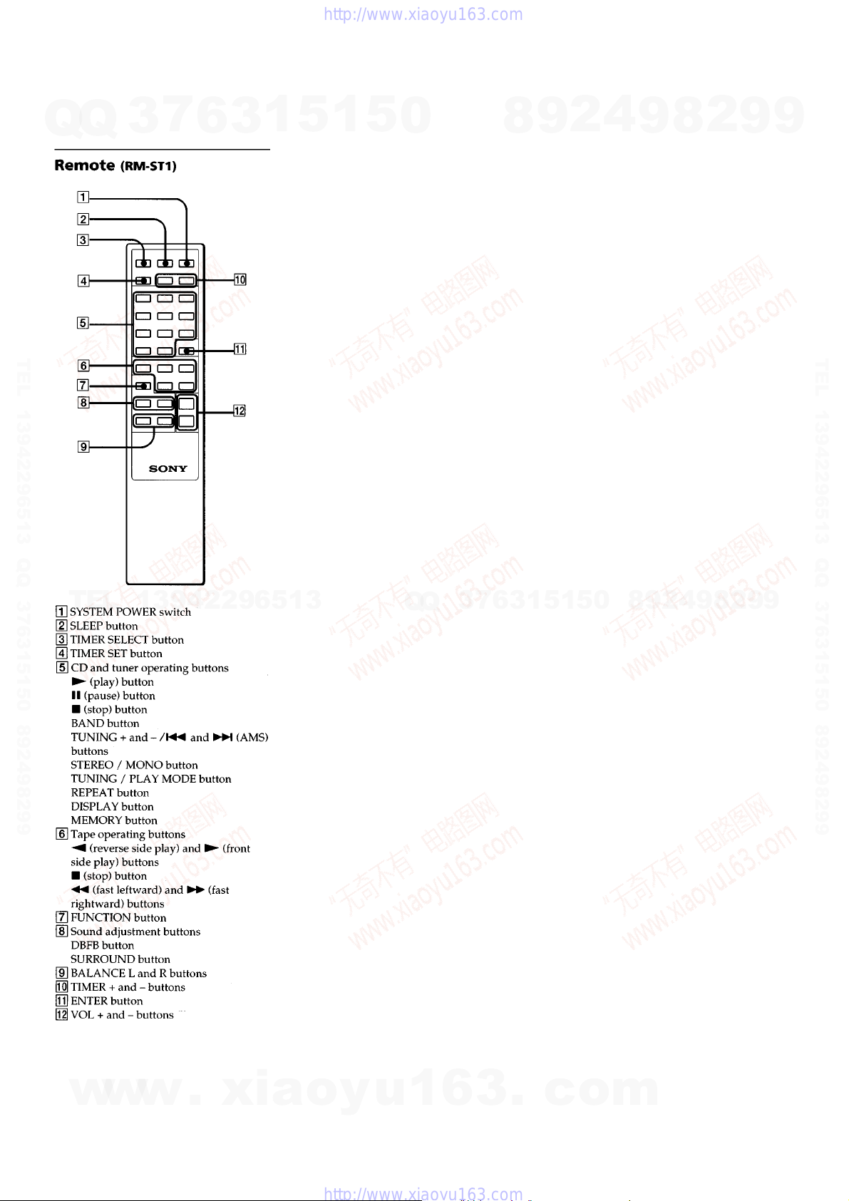
Index to Parts and Controls ............................................... 5
3. DISASSEMBLY............................................................ 7
4. ELECTRICAL ADJUSTMENTS
Tuner Section..................................................................... 11
CD Section......................................................................... 12
5. DIAGRAMS
5-1. Block Diagram................................................................... 14
5-2. Printed Wiring Board – BD Section – ............................... 18
5-3. Schematic Diagram – BD Section – .................................. 19
5-4. Schematic Diagram – Main Section – ............................... 22
5-5. Printed Wiring Boards – Main Section –
(US, Canadian model) ....................................................... 27
5-6. Printed Wiring Boards – Main Section –
(Except US, Canadian model) ........................................... 32
5-7. IC Pin Function Description .............................................. 38
6. EXPLODED VIEWS ................................................... 40
4
2
9
8
TABLE OF CONTENTS
....................................................... 4
9
8
2
9
9
TEL 13942296513 QQ 376315150 892498299
7. ELECTRICAL PARTS LIST .................................... 44
TEL
DISC TABLE GETTING OUT PROCEDURE ON THE POWER SUPPLY IS OFF
1. Insert the tweezers to a hole on bottom of the
chassis as shown a figure, then tern fully it
toward direction 2.
2. Open the door, pull out the disc table.
13942296513
1
tweezers
door
2
Q
Q
3
7
6
3
3
1
5
4
1
5
0
2
9
8
disc table
4
9
8
2
9
9
w
w
w
.
xia
o
y
u
1
6
3
– 2 –
cam
.
c
o
m
7
Q
Q
TEL 13942296513 QQ 376315150 892498299
TEL
3
SAFETY CHECK-OUT
After correcting the original service problem, perform the following safety check before releasing the set to the customer:
Check the antenna terminals, metal trim, “metallized” knobs, screws,
and all other exposed metal parts for AC leakage.
Check leakage as described below.
LEAKAGE TEST
The AC leakage from any exposed metal part to earth ground
and from all exposed metal parts to any exposed metal part ha ving a
return to chassis, must not exceed 0.5 mA (500 microampers.). Leakage current can be measured by any one of three methods.
1. A commercial leakage tester, such as the Simpson 229 or RCA
WT-540A. Follow the manufacturers’ instructions to use these
instruments.
2. A battery-operated AC milliammeter. The Data Precision 245
digital multimeter is suitable for this job.
3. Measuring the v oltage drop across a resistor by means of a V OM
or battery-operated A C voltmeter. The “limit” indication is 0.75
V, so analog meters must have an accurate low-voltage scale.
The Simpson 250 and Sanwa SH-63Trd are examples of a passive VOM that is suitable. Nearly all battery operated digital
multimeters that have a 2 V AC range are suitable. (See Fig. A)
13942296513
0.15 µF
6
To Exposed Metal
Parts on Set
3
1
1.5 k
5
Ω
1
5
AC
voltmeter
(0.75 V)
0
Q
Q
Laser component in this product is capable of emitting radiation
exceding the limit for Class 1.
CAUTION
Use of controls or adjustments or performance of
procedures other than those specified herein may
result in hazardous radiation exposure.
COMPONENTS IDENTIFIED BY MARK ! OR DOTTED
LINE WITH MARK ! ON THE SCHEMATIC DIAGRAMS
7
3
AND IN THE PARTS LIST ARE CRITICAL TO SAFE
OPERATION. REPLACE THESE COMPONENTS WITH
SONY PARTS WHOSE PART NUMBERS APPEAR AS
SHOWN IN THIS MANUAL OR IN SUPPLEMENTS PUBLISHED BY SONY.
4
2
9
8
SAFETY-RELATED COMPONENT WARNING!!
0
5
1
5
1
3
6
9
This appliance is classified as a
CLASS 1 LASER product.
The CLASS 1 LASER PRODUCT MARKING is located on the
rear exterior.
2
9
8
2
8
This caution label
is located inside
the unit.
8
9
4
9
2
9
9
TEL 13942296513 QQ 376315150 892498299
9
w
w
Earth Ground
Fig. A. Using an AC voltmeter to check AC leakage.
w
.
xia
o
y
u
1
ATTENTION AU COMPOSANT AYANT RAPPORT
LES COMPOSANTS IDENTIFIÉS P AR UNE MARQUE !
SUR LES DIAGRAMMES SCHÉMATIQUES ET LA LISTE
DES PIÈCES SONT CRITIQUES POUR LA SÉCURITÉ
DE FONCTIONNEMENT. NE REMPLACER CES COMPOSANTS QUE PAR DES PIÈCES SONY DONT LES
NUMÉROS SONT DONNÉS DANS CE MANUEL OU
DANS LES SUPPLÉMENTS PUBLIÉS PAR SONY.
6
3
.
À LA SÉCURITÉ!
c
o
m
– 3 –
Q
Q
3
7
6
3
1
SECTION 1
SERVICE NOTES
5
1
5
0
8
9
2
4
9
8
2
9
9
MODEL IDENTIFICATION
– Specification Label Printed on Back Panel –
HCD-D11/T11
MODEL NO.
TUNER CD PLAYER
TEL 13942296513 QQ 376315150 892498299
SERIAL NO.
MADE IN JAPAN
US, Canadian model : AC : 120 V 60 Hz 25 W
Except
US, Canadian model : AC : 120 V/220 – 240 V
TEL
13942296513
⁄
50/60 Hz 20 W (HCD-D11)
: AC : 120 V/220 – 240 V
⁄
50/60 Hz 25 W (HCD-T11)
NOTES ON HANDLING THE OPTICAL PICK-UP
BLOCK OR BASE UNIT
The laser diode in the optical pick-up block may suffer electrostatic
break-down because of the potential difference generated by the
charged electrostatic load, etc. on clothing and the human body.
During repair, pay attention to electrostatic break-down and also
use the procedure in the printed matter which is included in the
repair parts.
The flexible board is easily damaged and should be handled with
care.
NOTES ON LASER DIODE EMISSION CHECK
The laser beam on this model is concentrated so as to be focused on
the disc reflective surface by the objective lens in the optical pickup block. Therefore, when checking the laser diode emission, observe from more than 30 cm away from the objective lens.
Notes on chip component replacement
• Never reuse a disconnected chip component.
• Notice that the minus side of a tantalum capacitor may be dam-
aged by heat.
Flexible Circuit Board Repairing
• Keep the temperature of soldering iron around 270 ˚C during re-
pairing.
• Do not touch the soldering iron on the same conductor of the
circuit board (within 3 times).
• Be careful not to apply force on the conductor when soldering or
unsoldering.
Q
Q
3
7
6
3
1
5
1
5
0
8
9
2
4
9
8
2
9
TEL 13942296513 QQ 376315150 892498299
9
w
w
w
.
xia
o
y
u
1
6
3
– 4 –
.
c
o
m
SECTION 2
7
Q
Q
TEL 13942296513 QQ 376315150 892498299
3
6
3
1
5
1
5
GENERAL
0
8
9
2
4
This section is extracted
from instruction manual.
9
8
2
9
9
TEL 13942296513 QQ 376315150 892498299
TEL
13942296513
Q
Q
3
7
6
3
1
5
1
5
0
8
9
2
4
9
8
2
9
9
w
w
w
.
xia
o
y
u
1
6
3
– 5 –
.
c
o
m
7
Q
Q
TEL 13942296513 QQ 376315150 892498299
3
6
3
1
5
1
5
0
8
9
2
4
9
8
2
9
9
TEL 13942296513 QQ 376315150 892498299
TEL
13942296513
Q
Q
3
7
6
3
1
5
1
5
0
8
9
2
4
9
8
2
9
9
w
w
w
.
xia
o
y
u
1
6
3
– 6 –
.
c
o
m
SECTION 3
7
Q
Q
TEL 13942296513 QQ 376315150 892498299
3
Note: Follow the disassembly procedure in the numerical order given.
CASE
1
two screws
(case)
6
3
1
5
1
2
two screws (aluminum)
DISASSEMBLY
5
0
8
4
2
9
3
Remove the case in the
direction of the arrow.
9
8
2
9
9
TEL 13942296513 QQ 376315150 892498299
TEL
13942296513
FRONT PANEL ASS’Y
3
connector
(CN401)
2
ground terminal
1
wire (flat type) (15 core)
(CN505)
Q
Q
3
7
6
3
1
two screws
(case)
5
1
5
1
7
wire (flat type) (7 core)
(CN504)
0
8
9
2
4
2
8
9
8
front panel ass’y
9
9
w
w
5
Pull the front panel assy a little.
w
.
xia
4
four screws
(BTTM3
o
y
u
1
6
3
– 7 –
×
6)
6
wire (flat type) (13 core)
(CN501)
.
c
o
m
7
2
two screws
(BV3
6
3
×
10)
two covers
(pin jack 2P)
Q
Q
MAIN BOARD
TEL 13942296513 QQ 376315150 892498299
6
3
6
MAIN board
1
1
5
indication plate
(pin jack 6p)
1
5
0
2
screw (BV3 × 10)
4
two screws (BV3 × 10)
8
5
connector
(CN502)
9
2
4
9
3
two connectors
(CN203, 204)
8
2
9
9
TEL 13942296513 QQ 376315150 892498299
TEL
POWER BOARD
13942296513
4
POWER board
3
two screws
(BV3
9
9
2
8
9
4
2
9
8
0
5
1
5
1
3
6
7
3
Q
Q
2
three connectors
(CN201, 206, 801)
3
×
8)
screw
×
8)
(BV3
1
wire (flat type) (19 core)
(CN803)
w
w
w
.
xia
o
y
u
1
6
3
– 8 –
.
c
o
m
7
Q
Q
TEL 13942296513 QQ 376315150 892498299
3
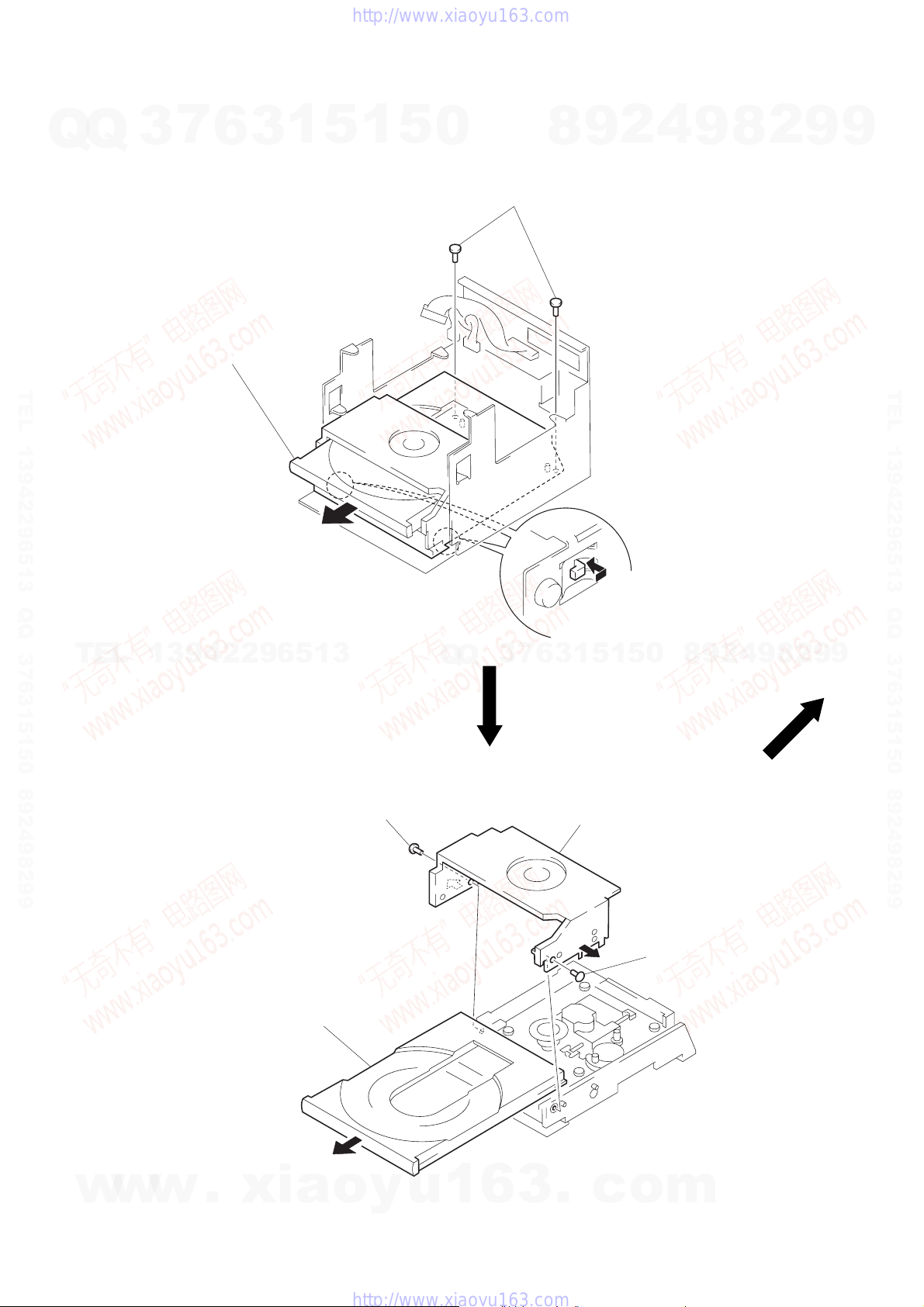
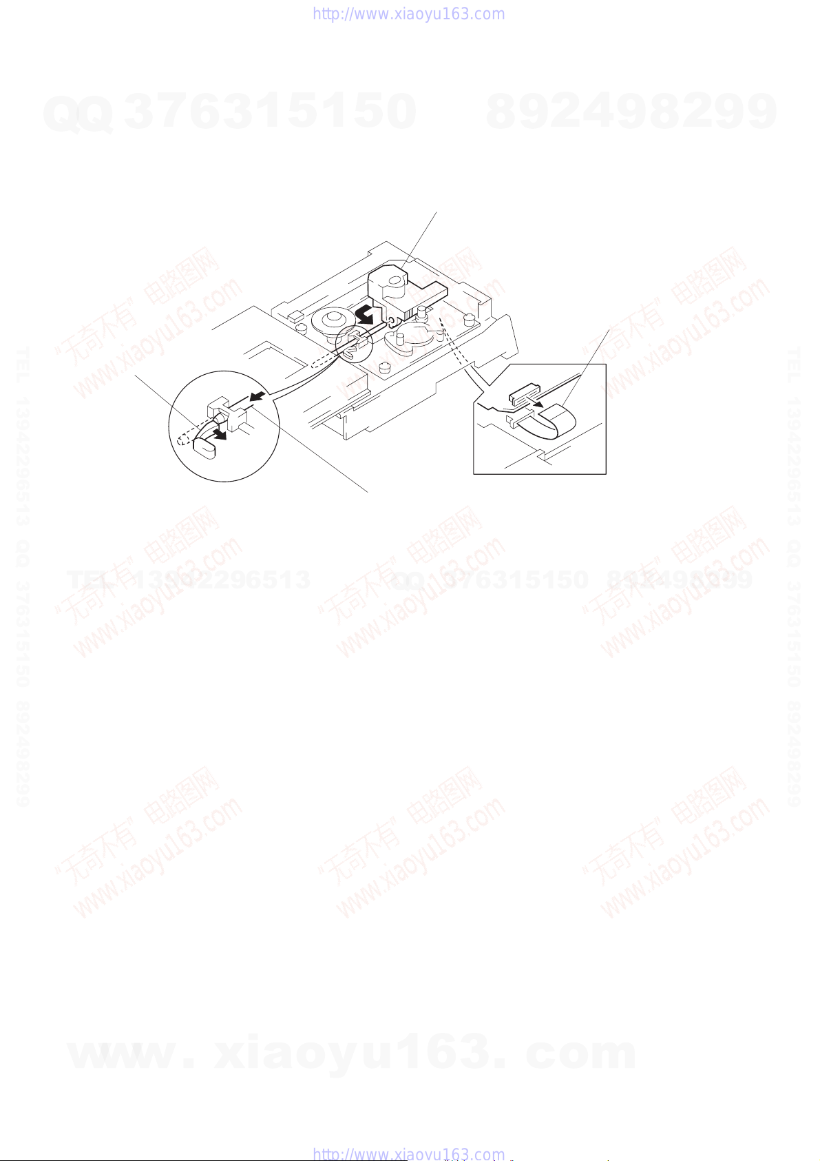
CD MECHANISM SECTION
3
6
CD mechanism section
3
1
5
1
5
0
1
two screws
(BV3
×
8)
8
9
2
4
9
8
2
9
9
TEL 13942296513 QQ 376315150 892498299
TEL
DISC T ABLE
13942296513
1
3
Pull the disc table
screw (BV3 × 8)
Q
Q
3
7
6
3
2
two hooks
5
1
2
8
0
5
1
holder (MG) ass’y
1
screw (BV3 × 8)
9
2
4
9
8
2
9
9
w
w
w
.
xia
o
y
u
1
6
3
– 9 –
.
c
o
m
7
Q
Q
OPTICAL PICK-UP
TEL 13942296513 QQ 376315150 892498299
1
3
Move the claw in the
direction of the arrow
6
A
.
3
B
A
1
5
1
5
0
4
C
2
Remove the sled shaft in the
direction of the arrow
Remove the optical pick-up
in the direction of the arrow
8
B
.
9
2
C
4
.
3
wire (flat type) (16 core)
(CNU101)
9
8
2
9
9
TEL 13942296513 QQ 376315150 892498299
TEL
13942296513
Q
Q
3
7
6
3
1
5
1
5
0
8
9
2
4
9
8
2
9
9
w
w
w
.
xia
o
y
u
1
6
3
– 10 –
.
c
o
m
set
FM RF SSG
+
–
level meter
J101 (OUTPUT)
FM ANTENNA
terminal (TM101)
Carrier frequency: 98 MHz
Output level: 1 mV (60 dB)
Modulation:
Main (1 kHz): 33.75 kHz dev. (45%)
Sub (1 kHz): 33.75 kHz dev. (45%)
Pilot (19 kHz): 7.5 kHz dev. (10%)
47 k
Ω
)
)
Q
Q
3
7
6
3
1
SECTION 4
ELECTRICAL ADJUSTMENTS
5
1
5
0
8
9
2
4
9
8
2
9
9
TUNER SECTION
As a front-end (TB101) is difficult to repair if faulty, replace it with
new one.
Please note, however, that the following adjustments are possible:
AM Section Adjustment
AM Tuned Level Adjustment
Note: FM Tuned Level Adjustment Should be performed after this
AM Tuned Lev el Adjustment.
Setting:
Band: AM or MW
loop antenna
TEL 13942296513 QQ 376315150 892498299
AM RF SSG
Carrier frequency: 999 kHz (at 9 kHz step)
Modulation: 400 Hz 30%
Output level: 6.3 mV (76 dB
Procedure:
1. Set AM RF SSG output level to 76 dBµ so that the input level
becomes 50 dBµ .
2. Tune the set to 999 kHz (at 9 kHz step) or 1,050 kHz (at 10 kHz
step).
TEL
13942296513
3. Adjust AM TUN (W) so that the TUNED light up.
Adjustment Location: Main board (TB101) (See page 13)
FM Section Adjustment
FM Tuned Level Adjustment
Setting:
Band: FM
0 dB=1 µV
60 cm
1,050 kHz (at 10 kHz step)
µ
)
loop antenna of
accessories
set
AM ANTENNA
terminal (TM101
Q
Q
FM Stereo Separation Adjustment
Setting:
Procedure:
Turn the set to 98 MHz.
signal generator
output channel
7
3
L-CH Stereo separation: A – B
R-CH Stereo separation: C – D
The separations of both channels should be equal.
Adjustment Location: Main board (TB101) (See page 13)
FM stereo
L-CH L-CH A
R-CH L-CH Adjust SEP (W) for
R-CH R-CH C
L-CH R-CH Adjust SEP (W) for
5
1
3
6
VTVM VTVM
connection reading (dB)
minimum reading.
minimum reading.
9
4
2
9
8
0
5
1
8
B
D
2
9
TEL 13942296513 QQ 376315150 892498299
9
FM RF SSG
Carrier frequency: 98 MHz
Modulation: 1 kHz, 75 kHz deviation
Output level: 17.8
Procedure:
1. Supply a 17.8 µV (25 dBµ ) 98 MHz signal to the ANTENNA
terminal.
2. Tune the set to 98 MHz.
3. Adjust FM TUN (W) so that the TUNED light up.
Adjustment Location: Main board (TB101) (See page 13)
w
w
w
FM ANTENNA terminal (TM101
set
µ
V (25 dBµ)
.
xia
o
y
u
1
6
3
.
– 11 –
c
o
m
+
–
BD board
TP (RF)
TP (VC)
oscilloscope
+
–
BD board
TP (TEO)
TP (VC)
oscilloscope
(DC range)
7
Q
Q
CD SECTION
Note:
1. CD Block basically constructed to operate without adjustment.
Therefore, check each item in order given.
2. Use YEDS-18 disc (3-702-101-01) unless otherwise indicated.
3. Use the oscilloscope with more than 10MΩ impedance.
4. Clean an object lens by an applicator with neutral detergent when
the signal level is low than specified value with the following
checks.
Focus Bias Adjustment
This adjustment is to be done when the optical block is replaced.
TEL 13942296513 QQ 376315150 892498299
Adjustment procedure:
1. Connect oscilloscope to test point TP (VC) and TP (RF) on BD
board.
2. Ground display board IC701 pin @¢ with the lead wire.
3. Turned power switch ON. (Stop mode)
4. Put disc (YEDS-18) in and press the ^ button.
5. Press the ^ button again. (Tracking servo ON)
6. Adjust RV101 so that the oscilloscope waveform is as shown in
TEL
the figure below (eye pattern).
A good eye pattern means that the diamond shape (≈) in the
center of the waveform can be clearly distinguished.
7. Remove the lead wire connected in step2.
• RF signal reference waveform (eye patter n)
3
BD board
TP (RF)
TP (VC)
13942296513
6
1
3
oscilloscope
(DC range)
+
–
level:
1.3
5
1
5
VOLT/DIV: 200 mV
TIME/DIV: 500 ns
±
0.3Vp-p
0
actuate the focus search. (actuate the focus search when disc
table is moving in and out.)
5. Check the oscilloscope waveform (S-curve) is symmetrical between A and B. And conf irm peak to peak le v el within 2.4 ± 0.7
Vp-p.
S-curve wavef orm
6. After check, remove the lead wire connected in step 2.
Note: • Try to measure several times to make sure that the ratio of
A:B or B:A is more than 10:7.
• Take sweep time as long as possible and light up the bright-
ness to obtain best waveform.
RF Level Check
Procedure:
1. Connect oscilloscope to test point TP (VC) and TP (RF) on BD
board.
2. Turned Power switch on.
Q
Q
3. Put disc (YEDS-18) in and press the ^ button.
4. Confirm that oscilloscope waveform is clear and check RF sig-
Note: Clear RF signal waveform means that the shape “≈” can be
7
3
nal level is correct or not.
clearly distinguished at the center of the waveform.
RF signal waveform
8
6
3
9
1
5
2
1
5
4
0
9
symmetry
A
within 2.4
B
9
8
VOLT/DIV: 200 mV
TIME/DIV: 500 ns
level:
1.3
8
4
2
±
0.3Vp-p
2
±
0.7 Vp-p
8
9
9
2
9
9
TEL 13942296513 QQ 376315150 892498299
9
When observing the eye pattern, set the oscilloscope for AC
range and raise vertical sensitivity.
S-Curve Check
oscilloscope
BD board
TP (FEO)
TP (VC)
Procedure:
1. Connect oscilloscope to test point TP (VC) and TP (FEO) on
BD board.
2. Connect between test point TP (FOK) and Ground by lead wire.
3. Turned Power switch on.
4. Put disc (YEDS-18) in and turned Power switch on again and
w
w
w
+
–
.
xia
o
y
E-F Balance (Traverse) Check
Procedure:
1. Ground display board IC701 pin @¢ with the lead wire.
2. Connect oscilloscope to test point TP (TEO) on BD board.
3. Turned Power switch on.
4. Put disc (YEDS-18) in and press the ^ button.
5. Confirm that the oscilloscope waveform is symmetrical on the
top and bottom in relation to 0V, and check this level.
u
1
6
3
.
c
o
m
– 12 –
 Loading...