

Sony HCD-RV22, HCD-RV55 Service Manual

HCD-RV22/RV55
SERVICE MANUAL
Ver 1.1 2004. 08
• HCD-RV22/RV55 are the tuner,
deck, CD and amplifier
section in MHC-RV22/RV55.
(Photo: HCD-RV55)
CD CD Mechanism Type CDM74-K4BD49
Section Base Unit Name BU-K4BD49
TAPE HCD-RG330
Section
E Model
Model Name Using Similar Mechanism NEW
Optical Pick-up Name KSM-213DHAP
Model Name Using Similar Machanism
Tape Mechanism Type
HCD-GN700
CWM43RR35
CWM43FF13
Amplifier section
HCD-RV55
Front speaker
The following measured at AC 120, 127, 220, 240 V, 50/60 Hz
DIN power output (rated):
120 + 120 watts
(6 ohms at 1 kHz, DIN)
Continuous RMS power output (reference):
150 + 150 watts
(6 ohms at 1 kHz, 10% THD)
HCD-RV22
The following measured at AC 120, 127, 220, 240 V, 50/60 Hz
DIN power output (rated):
100 + 100 watts
(6 ohms at 1 kHz, DIN)
Continuous RMS power output (reference):
120 + 120 watts
(6 ohms at 1 kHz, 10% THD)
SPECIFICATIONS
Inputs
VIDEO/SAT IN (phono jacks) (HCD-RV55 only):
voltage 450/250 mV,
impedance 47 kilohms
GAME INPUT AUDIO L/R (phono jacks):
voltage 250 mV,
impedance 47 kilohms
GAME INPUT VIDEO (phono jack):
1 Vp-p, 75ohms
MIC (phone jack): sensitivity 1 mV,
impedance 10 kilohms
Outputs
PHONES (stereo phone jack):
accepts headphones of
8 ohms or more
VIDEO/SAT OUT (phono jacks) (HCD-RV55 only):
impedance 1 kilohm
– Continued on next page –
MINI Hi-Fi COMPONENT SYSTEM
9-879-126-02
2004H04-1
© 2004. 08
Sony Corporation
Audio Group
Published by Sony Engineering Corporation
1

HCD-RV22/RV55
VIDEO OUT (phono jack):
SPEAKER: accepts impedance of 6 to
SURROUND SPEAKER (HCD-RV55 only):
max. output level 1 Vp-p,
unbalanced, Sync negative
load impedance 75 ohms
16 ohms
accepts impedance of
24 ohms
CD player section
System Compact disc and digital
Laser Semiconductor laser
Frequency response 2 Hz – 20 kHz (±0.5 dB)
Signal-to-noise-ratio More than 90 dB
Dynamic range More than 90 dB
Video color system format
audio system
(λ=770 – 810 nm)
Emission duration:
continuous
NTSC, PAL
Tape deck section
Recording system 4-track 2-channel, stereo
Frequency response 50 – 13,000 Hz (±3 dB),
using Sony TYPE I cassettes
Tuner section
FM stereo, FM/AM superheterodyne tuner
FM tuner section
Tuning range 87.5 – 108.0 MHz
Antenna FM lead antenna
Antenna terminals 75 ohms unbalanced
Intermediate frequency 10.7 MHz
AM tuner section
Tuning range
Saudi Arabian model: 531 – 1,602 kHz
Other models: 530 – 1,710 kHz
Antenna AM loop antenna
Antenna terminals External antenna terminal
Intermediate frequency 450 kHz
(50 kHz step)
(with the tuning interval
set at 9 kHz)
(with the tuning interval
set at 10 kHz)
531 – 1,602 kHz
(with the tuning interval
set at 9 kHz)
General
Power requirements
Saudi Arabian model: 120 – 127/220 or 230 – 240 V AC,
50/60 Hz
Adjustable with voltage selector
Thai model: 220 V AC, 50/60 Hz
Other models: 120 V, 220 V or 230 – 240 V AC,
50/60 Hz
Adjustable with voltage selector
Power consumption
HCD-RV55: 150 watts
HCD-RV22: 180 watts
Dimensions (w/h/d) incl.projecting parts and controls
Amplifier/Tuner/Tape/CD Section:
Approx. 280 × 327 × 425 mm
Mass
HCD-RV55: Approx. 10.6 kg
HCD-RV22: Approx. 10.1 kg
Supplied accessories: Remote Commander (1)
R6 (Size AA) batteries (2)
AM loop antenna (1)
FM lead antenna (1)
Speaker pads (8)
Video cable (1)
Design and specifications are subject to change without
notice.
SAFETY-RELATED COMPONENT WARNING!!
COMPONENTS IDENTIFIED BY MARK 0 OR DOTTED LINE
WITH MARK 0 ON THE SCHEMATIC DIAGRAMS AND IN
THE PARTS LIST ARE CRITICAL TO SAFE OPERATION.
REPLACE THESE COMPONENTS WITH SONY P ARTS WHOSE
PART NUMBERS APPEAR AS SHOWN IN THIS MANUAL OR
IN SUPPLEMENTS PUBLISHED BY SONY.
2
HCD-RV22/RV55
Notes on Chip Component Replacement
• Never reuse a disconnected chip component.
• Notice that the minus side of a tantalum capacitor may be
damaged by heat.
Flexible Circuit Board Repairing
• Keep the temperature of soldering iron around 270°C during
repairing.
• Do not touch the soldering iron on the same conductor of the
circuit board (within 3 times).
• Be careful not to apply force on the conductor when soldering
or unsoldering.
UNLEADED SOLDER
Boards requiring use of unleaded solder are printed with the lead
free mark (LF) indicating the solder contains no lead.
(Caution: Some printed circuit boards may not come printed with
the lead free mark due to their particular size)
: LEAD FREE MARK
Unleaded solder has the following characteristics.
• Unleaded solder melts at a temperature about 40 °C higher than
ordinary solder.
Ordinary soldering irons can be used but the iron tip has to be
applied to the solder joint for a slightly longer time.
Soldering irons using a temperature regulator should be set to about
350 °C.
Caution: The printed pattern (copper foil) may peel away if the
heated tip is applied for too long, so be careful!
• Strong viscosity
Unleaded solder is more viscou-s (sticky , less prone to flo w) than
ordinary solder so use caution not to let solder bridges occur such
as on IC pins, etc.
• Usable with ordinary solder
It is best to use only unleaded solder but unleaded solder may also
be added to ordinary solder.
NOTES ON LASER DIODE EMISSION CHECK
The laser beam on this model is concentrated so as to be focused on
the disc reflective surface by the objective lens in the optical pickup block. Therefore, when checking the laser diode emission,
observe from more than 30 cm away from the objective lens.
Laser component in this product is capable
of emitting radiation exceeding the limit for
Class 1.
This appliance is
claassified as a CLASS 1
LASER product. This
label is located on the
rear exterior.
CAUTION
Use of controls or adjustments or performance of procedures
other than those specified herein may result in hazardous
radiation exposure.
NOTES ON HANDLING THE OPTICAL PICK-UP BLOCK
OR BASE UNIT
The laser diode in the optical pick-up block may suffer electrostatic
breakdown because of the potential difference generated by the
charged electrostatic load, etc. on clothing and the human body.
During repair, pay attention to electrostatic break-down and also
use the procedure in the printed matter which is included in the
repair parts.
The flexible board is easily damaged and should be handled with
care.
3
HCD-RV22/RV55
MODEL IDENTIFICATION
– BACK PANEL –
Part No.
MODEL PARTS No.
RV22: PH 4-254-522-0s
RV22: EA 4-254-523-0s
RV22: TH 4-254-524-0s
RV55: PH 4-254-528-0s
RV22: E3, E15 4-254-800-0s
RV22: MY, SP 4-254-802-0s
RV55: E3, E15 4-254-803-0s
RV55: MY, SP 4-254-804-0s
RV55: EA 4-254-807-0s
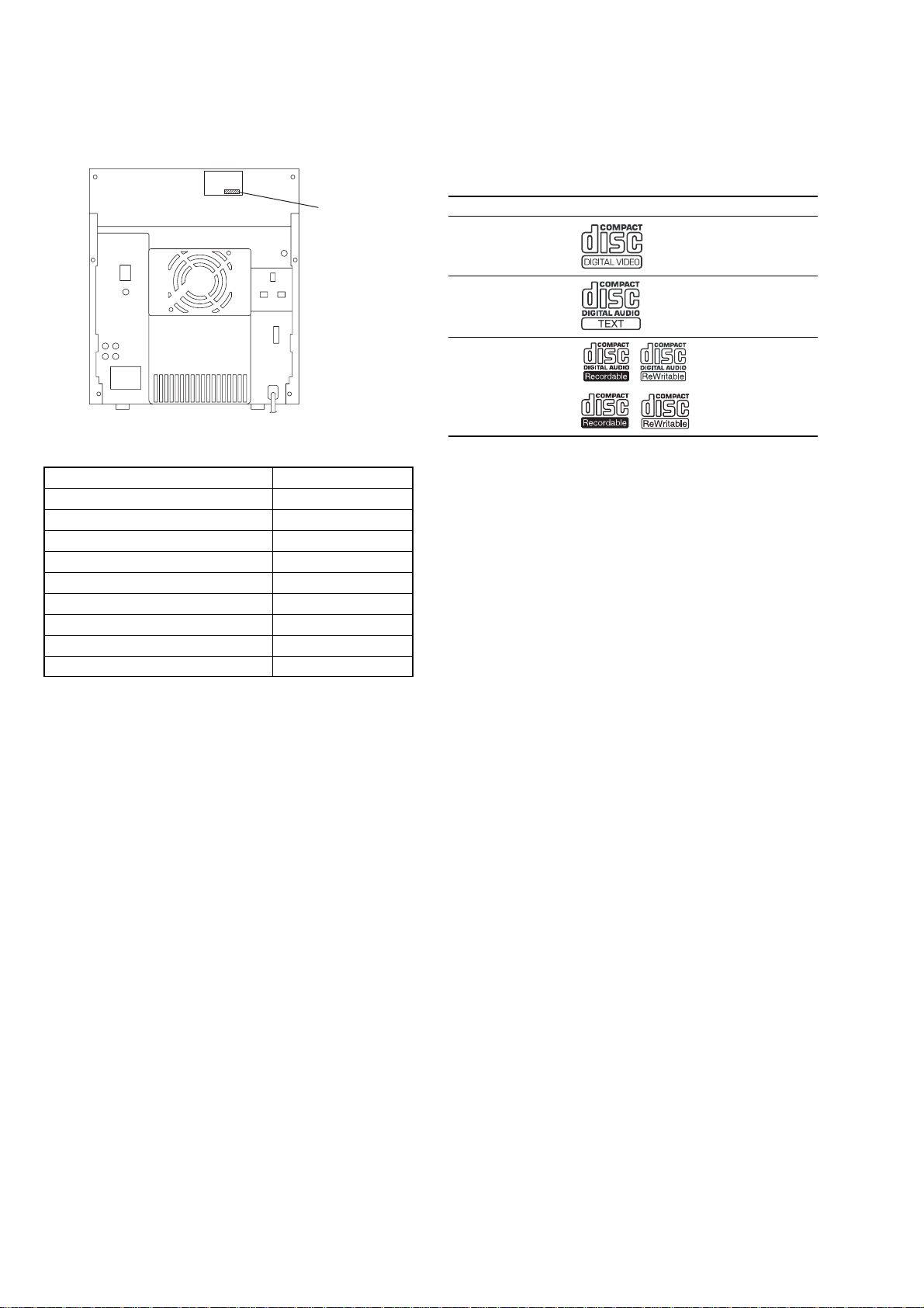
PLAYABLE DISC
You can playback the following discs on this system. The other
discs cannot be played back.
List of playable discs
Format of discs Disc logo
VIDEO CDs
Audio CDs
CD-R/CD-RW
(audio data/MP3
files)
• Abbreviation
E3 : 240 V AC area in E model
E15 : Iran model
PH : Philippine model
EA : Saudi Arabia model
TH : Thai model
4

TABLE OF CONTENTS
HCD-RV22/RV55
1. SERVICE NOTE
1-1. Service Position of CD Mechanism Deck........................... 6
1-2. Service Position of Amp Board........................................... 6
2. GENERAL
List of Button Locations and Reference Pages........................ 7
3. DISASSEMBLY
3-1. Case (Top) ......................................................................... 10
3-2. CD Door ............................................................................ 10
3-3. Front Panel Section ........................................................... 11
3-4. CD Mechanism Deck ........................................................ 11
3-5. Tape Mechanism Deck, Mic Board ...................................12
3-6. Panel Board ....................................................................... 12
3-7. Back Panel Section, Sub Trans Board ...............................13
3-8. Trans Board .......................................................................13
3-9. Main Board ....................................................................... 14
3-10. Amp Board ........................................................................ 14
3-11. BD49 Board ...................................................................... 15
3-12. VCD Connect Board, VMP43GY Board .......................... 15
3-13. Driver Board, SW Board...................................................16
3-14. Optical Pick-up ................................................................. 16
3-15. Sensor Board ..................................................................... 17
3-16. Motor (TB) Board ............................................................. 17
3-17. Motor (LD) Board ............................................................. 18
4. TEST MODE ..................................................................... 19
5. ELECTRICAL ADJUSTMENTS................................. 23
6. DIAGRAMS
6-1. Circuit Boards Location .................................................... 25
6-2. Printed Wiring Board –CD Mechanism Section (1/2)– .... 28
6-3. Schematic Diagram –CD Mechanism Section (1/2)– ....... 29
6-4. Printed Wiring Boards –CD Mechanism Section (2/2)–... 30
6-5. Schematic Diagram –CD Mechanism Section (2/2)– ....... 31
6-6. Printed Wiring Board –VCD Connect Section–................ 32
6-7. Schematic Diagram –VCD Connect Section– .................. 32
6-8. Printed Wiring Board –VMP Section–..............................33
6-9. Schematic Diagram –VMP Section (1/2)–........................ 34
6-10. Schematic Diagram –VMP Section (2/2)–........................ 35
6-11. Schematic Diagram –Main Section (1/2)– ........................36
6-12. Schematic Diagram –Main Section (2/2)– ........................37
6-13. Printed Wiring Board –Main Section– .............................. 38
6-14. Printed Wiring Boards –Panel Section– ............................ 39
6-15. Schematic Diagram –Panel Section (1/2)– ....................... 40
6-16. Schematic Diagram –Panel Section (2/2)– ....................... 41
6-17. Printed Wiring Boards –Jack Section–..............................42
6-18. Schematic Diagram –Jack Section– .................................. 43
6-19. Printed Wiring Board
–Power Section (1/2) (HCD-RV22)– ................................ 44
6-20. Printed Wiring Boards
–Power Section (2/2) (HCD-RV22)– ................................ 45
6-21. Schematic Diagram –Power Section (HCD-RV22)– ........ 46
6-22. Schematic Diagram –Power Section (HCD-RV55)– ........ 47
6-23. Printed Wiring Board
–Power Section (1/2) (HCD-RV55)– ................................ 48
6-24. Printed Wiring Boards
–Power Section (2/2) (HCD-RV55)– ................................ 49
6-25. IC Block Diagrams............................................................ 50
7. EXPLODED VIEWS
7-1. Main Section ..................................................................... 60
7-2. Front Panel Section (1)...................................................... 61
7-3. Front Panel Section (2)...................................................... 62
7-4. Front Panel Section (3)...................................................... 63
7-5. Main Board Section .......................................................... 64
7-6. CD Mechanism Deck Section (1) ..................................... 65
7-7. CD Mechanism Deck Section (2) ..................................... 66
7-8. CD Mechanism Deck Section (3) ..................................... 67
7-9. Base Unit Section ..............................................................68
8. ELECTRICAL PARTS LIST ........................................ 69
5
HCD-RV22/RV55
d
k
SECTION 1
SERVICE NOTE
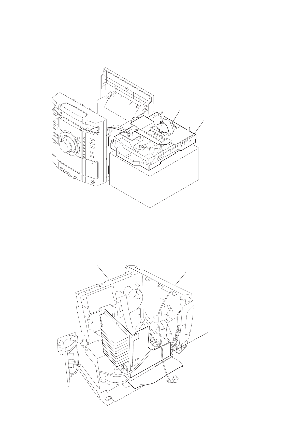
1-1. SERVICE POSITION OF CD MECHANISM DECK
Remove the CD mechanism deck and place it on top of the pedestal as shown.
Inspect the BD49 board in this set up.
BD49 board
CD mechanism dec
1-2. SERVICE POSITION OF AMP BOARD
To inspect the AMP board, turn both of the front panel
and the CD mechanism deck so that the left side of the product faces down.
CD mechanism deck
front panel
AMP boar
6

SECTION 2
GENERAL
HCD-RV22/RV55
This section is extracted
from instruction manual.
7

HCD-RV22/RV55
8

Note : Disassemble the unit in the order as shown below.
SET
3-1. CASE (TOP)
(Page 10)
3-2. CD DOOR
(Page 10)
3-3. FRONT PANEL SECTION
(Page 11)
HCD-RV22/RV55
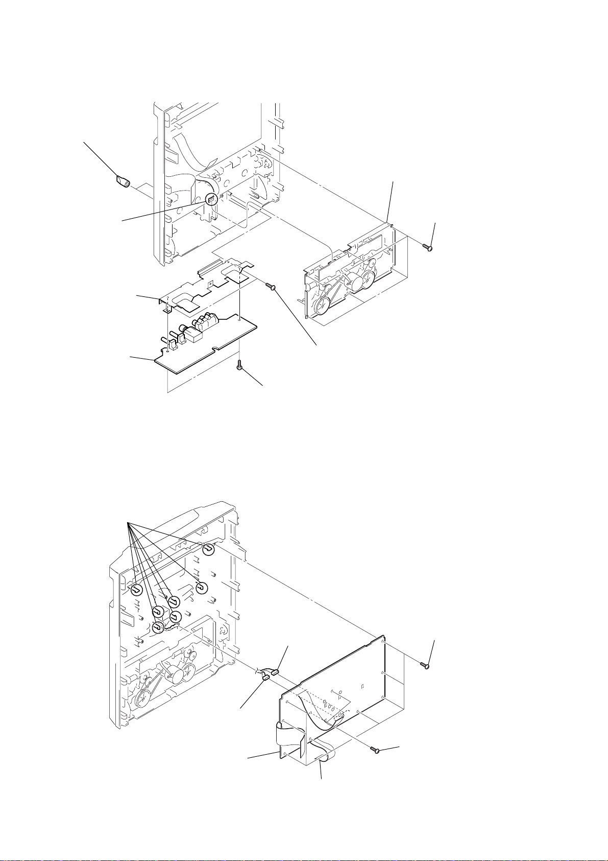
SECTION 3
DISASSEMBLY
3-4. CD MECHANISM DECK
(Page 11)
3-12. VCD CONNECT BOARD,
VMP43GY BOARD
(Page 15)
3-13. DRIVER BOARD,
SW BOARD
(Page 16)
3-7. BACK PANEL SECTION,
SUB TRANS BOARD
(Page 13)
3-5. TAPE MECHANISM DECK,
MIC BOARD
(Page 12)
3-11. BD49 BOARD
(Page 15)
3-14. OPTICAL PICK-UP
(Page 16)
3-6. PANEL BOARD
(Page 12)
3-15. SENSOR BOARD
(Page 17)
3-16. MOTOR (TB) BOARD
(Page 17)
3-17. MOTOR (LD) BOARD
(Page 18)
3-8. TRANS BOARD
(Page 13)
3-9. MAIN BOARD
(Page 14)
3-10. AMP BOARD
(Page 14)
9

HCD-RV22/RV55
Note : Follow the disassembly procedure in the numerical order given.
3-1. CASE (TOP)
qf
qh
case
(top)
7
two
screws
(case 3 TP2)
qs
0
(+BVTP 3
8
screw
(case 3 TP2)
screw
case (side-L)
9
screw
(+BVTP 3
×
10)
×
qg
10)
qa
qd
two
screws
(+BVTP 3
qf
5
×
10)
6
case (side-R)
3
(+BVTP 3
1
two
(case 3 TP2)
screw
screws
×
10)
3-2. CD DOOR
CD mechanism deck (CDM74)
1
Turn the pulley to the direction of the arrow.
pulley
Front panel side
2
Pull-out the disc tray.
3
four claws
2
(case 3 TP2)
4
CD door
4
(+BVTP 3
screw
screw
×
10)
10
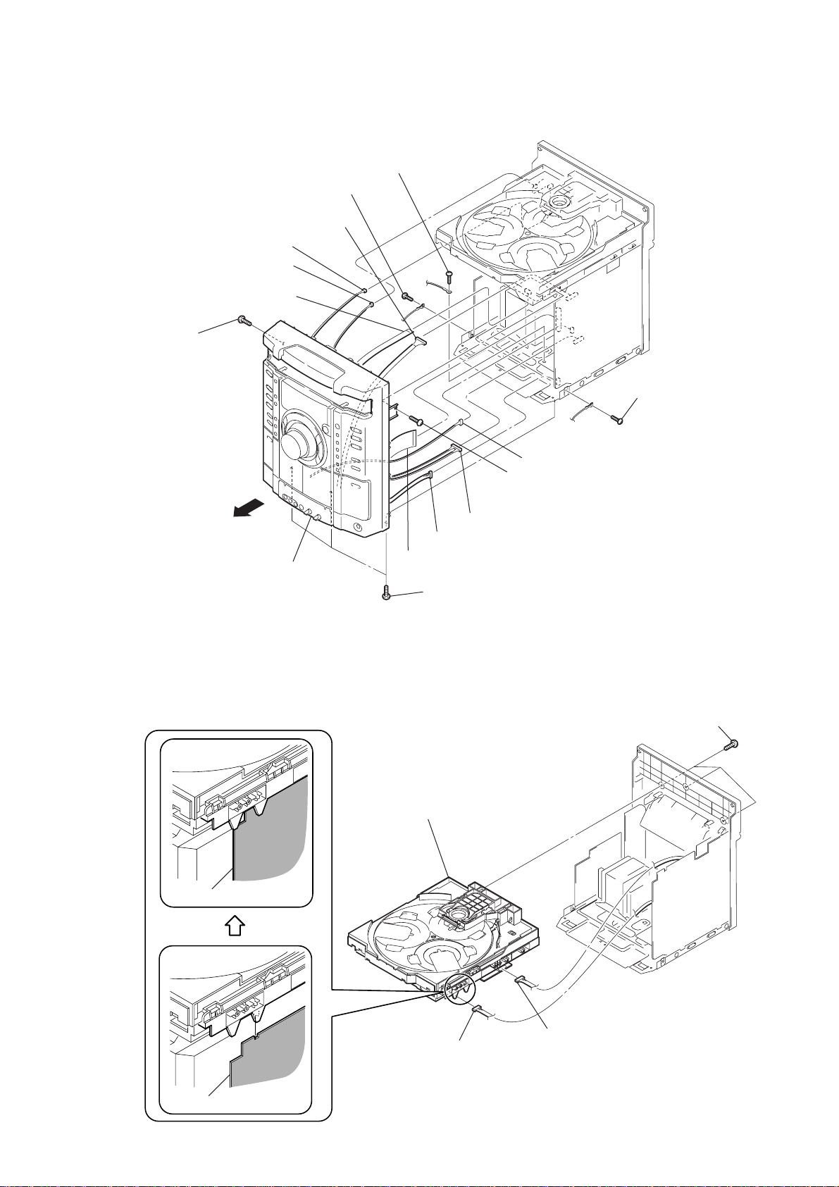
3-3. FRONT PANEL SECTION
qg
CN301 (3P)
1
CN805 (2P)
3
CN823 (11P)
8
screw
(+BVTP 3
×
10)
4
screw
(+BVTP 3
qa
CN304 (8P)
qf
×
screw
(+BV (3
8)
−
CR))
HCD-RV22/RV55
5
screw (+BVTP 3
×
8)
9
qh
front panel section
3-4. CD MECHANISM DECK
0
CN309 (5P)
2
CN302 (29P)
6
three
(+BVTP 3
4
CD mechanism deck
qd
CN103 (8P)
screws
×
8)
qs
CN102 (3P)
7
screw (+BVTP 3
×
10)
1
three
(+BVTP 3
screws
×
10)
MAIN board
MAIN board
3
CN883 (11P)
2
CN701 (12P)
11
HCD-RV22/RV55
)
)
3-5. TAPE MECHANISM DECK, MIC BOARD
4
two MIC knobs
1
connector
jack bracket
3
tape mechanism deck
2
six
(+BVTP 2.6
screws
×
8
7
MIC board
3-6. PANEL BOARD
4
seven
claws
6
two
(+BVTP 3
screws
×
6
CN604 (6P)
5
two
(+BVTP 2.6
8)
screws
×
8)
2
eight
screws
(+BVTP 2.6
×
8
12
5
7
PANEL board
CN605 (5P)
1
connector (13P)
3
two
(+BVTP 2.6
screws
×
8)
3-7. BACK PANEL SECTION, SUB TRANS BOARD
1
CN905 (5P)
2
CN907 (10P)
4
earth wire
3
screw
(+BVIT 3
× 8R
)
5
four
screws
(screw)
6
TRANS board
qa
SUB TRANS board
3
CN901 (2P)
0
two
screws
×
10)
4
CN101 (11P)
CN906 (7P)
2
1
CN904 (4P)
(+BVTP 3
9
5
CN308 (3P)
qs
back panel section
HCD-RV22/RV55
7
two
screws
(+BVTP 3
8
6
screw
(+BVTP 3
two
screws
(+BVTP 3
×
×
×
10)
10)
10)
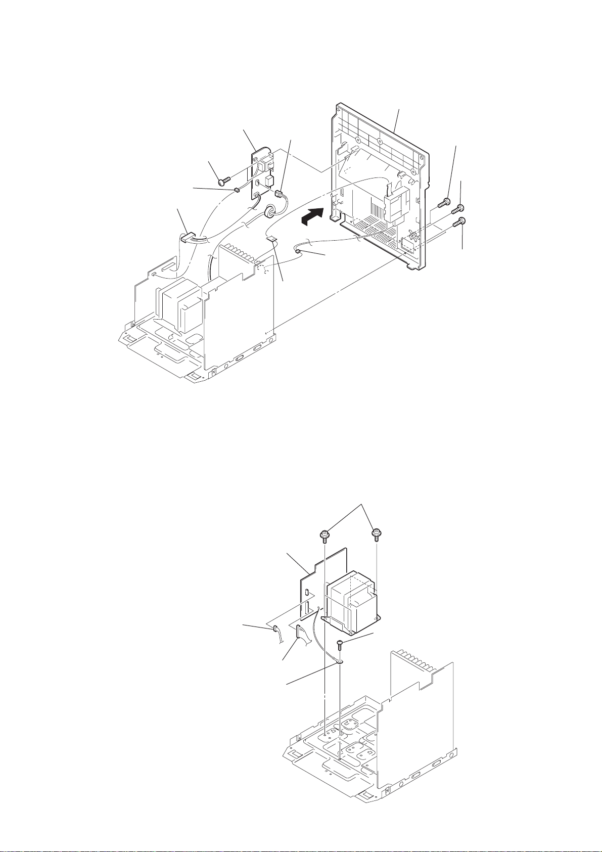
3-8. TRANS BOARD
13
HCD-RV22/RV55
3-9. MAIN BOARD
1
CN907 (10P)
4
MAIN board
MAIN board
3-10. AMP BOARD
4
screw
(+BV (3
5
two
(transistor)
8
AMP
screws
board
−
CR))
3
screw
(+BVTP 3
×
14)
3
2
two
(+BVTP 3
CN441
screws
6
×
8)
2
two
screws
×
(+BVTT 4
7
heat sink
8)
14
1
CN905 (5P)

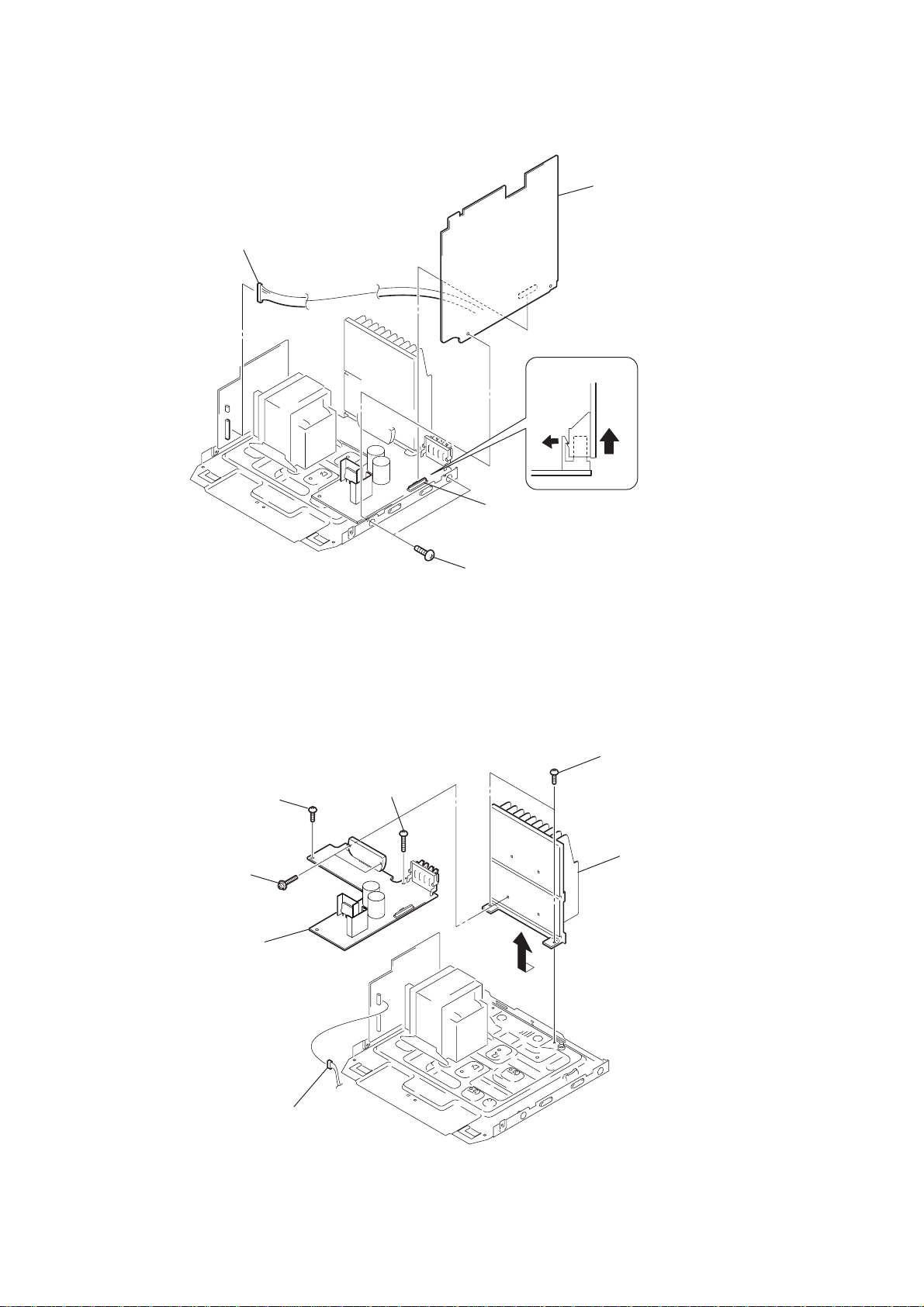
3-11. BD49 BOARD
d
5
Remove soldering from the four points.
1
CN101 (29P)
3
screw
(+BVTP 2.6
6
4
BD49
HCD-RV22/RV55
× 8
)
gap tube
board
2
CN102 (16P)
3-12. VCD CONNECT BOARD, VMP43GY BOARD
1
2
two
(+BVTP 2.6
3
VCD CONNECT
screws
board
× 8
)
CN881 (19P)
4
CN101 (29P)
5
two
screws
(+BVTP 2.6
6
× 8
)
VMP43GY
boar
15

HCD-RV22/RV55
3-13. DRIVER BOARD, SW BOARD
1
two
screws
(+BTTP (M2.6))
4
DRIVER
2
board
CN702 (5P)
3
CN703 (4P)
5
screw
(+BTTP (M2.6))
6
SW board
3-14. OPTICAL PICK-UP
8
optical pick-up
(BU-K4BD49)
7
three
insulators
6
three
(insulator)
coil springs
4
(BVTT M2.6)
three
screws
5
three
3
1
floating
(+PTPWH M2.6)
stoppers (BU)
insulator
2
coil spring
(insulator)
screw
16
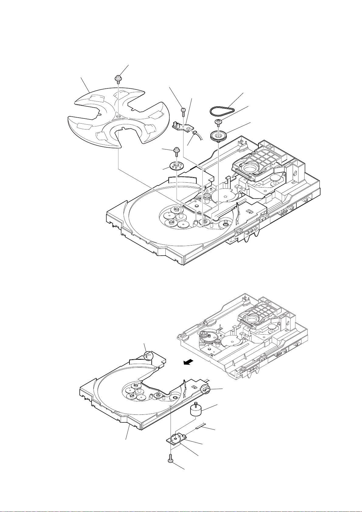
3-15. SENSOR BOARD
2
t
ray
1
floating
(+PTPWH M2.6)
6
floating
(+PTPWH M2.6)
7
g
screw
8
(+BTTP (M2.6))
screw
ear (geneva)
s
crew
0
SENSOR board
9
CN731 (3P)
3
b
elt (table)
4
floating
(+PTPWH M2.6)
5
screw
p
ulley (table)
HCD-RV22/RV55
3-16. MOTOR (TB) BOARD
table assy
2
stopper
4
stopper
1
7
t
able motor assy (M741)
3
CN742 (5P)
8
MOTOR (TB) board
6
Remove the two solderings of motor.
5
two
screws
(+BTTP (M2.6))
17

HCD-RV22/RV55
3-17. MOTOR (LD) BOARD
4
Remove the two solderings of motor.
5
l
oading motor assy (M751)
2
two
screws
(+BTTP (M2.6))
3
MOTOR (LD) board
1
b
elt (loading)
18

SECTION 4
TEST MODE
HCD-RV22/RV55
MC COLD RESET
The cold reset clears all data including preset data stored in the
RAM to initial conditions. Execute this mode when returning the
set to the customer.
Procedure:
1. Press the I/1 button to turn the power ON.
2. Press three buttons of x , [PLAY MODE/TUNING MODE] and
[DISC 1] simultane-ously.
3. The message “COLD RESET” is displayed on the fluorescent
indicator tube momentarily, then becomes standby states.
AM TUNING INTERVAL CHANGE-OVER
A step of AM tuning interval can be changed over between 9 kHz
and 10 kHz.
Procedure:
1. Press the I/1 button to turn the power on.
2. Press the [TUNER/BAND] button to select “AM”.
3. Press the I/1 button to turn the power off.
4. Press two buttons of [PLAY MODE/TUNING MODE] and I/1
simultaneously.
5. The message “ AM 9K STEP” or “ AM 10K STEP” is displayed
on the fluorescent indicator tube, and thus the channel step is
changed over.
CD SHIP (LOCK) MODE
This mode moves the optical pick-up to the position durable to
vibration. Use this mode when returning the set to the customer
after repair.
Procedure:
1. Press the I/1 button to turn the power on.
2. Press the [CD] button to select “CD”.
3. Press two buttons of [CD] and I/1 simultaneously.
4. The message “LOCK” is displayed on the fluorescent indicator
tube, and the CD ship mode is set.
CD SHIP (LOCK) MODE & COLD RESET
This mode is used to perform CD chip (lock) mode and cold reset
simultaneously.
Procedure:
1. Press the I/1 button to turn the power on.
2. Press the [CD] button to select “CD”.
3. Press three buttons of x , [CD] and I/1 simultaneously.
4. The message “COLD RESET” is displayed on the fluorescent
indicator tube momentarily, then becomes standby states.
CHANGE-OVER FUNCTION OF SAT/VIDEO
This mode is used to enable function of external input to change
over between SAT and VIDEO.
Procedure:
1. Press the I/1 button to turn the power on.
2. Press two buttons of VIDEO/SAT and I/1 simultaneously.
3. The message “SAT” or “VIDEO”is displayed on the
fluorescent indicator tube, and the function of external input
is changed over.
CD TRAY LOCK MODE
This mode is used to unable to take sample disc out of tray in the
shop.
Procedure:
1. Press the
2. Press the [CD] button to select “CD”.
3. Set disc on the CD tray, press two buttons of
seconds.
4. The message “LOCKED” is displayed on the fluorescent
indicator tube and the CD tray is locked. (Even if pressing
the Z button, the message “LOCKED” is displayed on the
fluorescent indicator tube and the CD tray is locked)
5. To release from this mode, press two buttons of x and Z for
5 seconds.
6. The message “UNLOCKED” is displayed on the fluorescent
indicator tube and the CD tray is unlocked.
I/1 button to turn the power on.
x and Z for 5
AMP TEST MODE
This mode is used to display the parameter of amplifier IC and
display the VACS status.
Procedure:
1. Press the I/1 button to turn the power on.
2. Press three buttons of x , [PRESET EQ] and [PLAY MODE/
TUNING MODE] simultaneously.
3. When the AMP test mode is activated, the message “AMP
TEST IN” is displayed on the fluorescent indicator tube
momentarily, then amplif ier adjustment mode is displayed on
the fluorescent indicator tube.
4. Press the [DISPLAY] button to changed over between VACS
status display mode and the amplifier IC parameter display
mode.
5. In the amplifier IC parameter display mode, press the
[GROOVE] button to changed over DBFB on/off, and when it
is on, the character “D” is displayed on the fluorescent indicator
tube.
6. In the amplifier IC parameter display mode, press the
[SURROUND] button to changed over surround on/off, and
when it is on, the character “S” is displayed on the fluorescent
indicator tube.
7. In the amplifier IC parameter display mode, turn each knob of
. >
[ -- EQ + ] causes respective parameters to be changed,
as well as change-over of the display on the fluorescent
indicator tube.
CD SERVICE MODE
This mode can run the CD sled motor freely. Use this mode, for
instance, when cleaning the optical pick-up.
Procedure:
1. Press the I/1 button to turn the power on.
2. Press the [CD] button to select “CD”.
3. Press three buttons of x , [PLAY MODE/TUNING MODE] and
Z simultaneously.
4. When the CD service mode is activated, the message “MPEG
AV TEST” is displayed on the fluorescent indicator tube.
5. Press the M button, optical pick-up move to outside track
and the message “SLED OUT” is displayed on the fluorescent
indicator tube.
6. Press the m button, optical pick-up move to inside track and
the message “SLED IN” is displayed on the fluorescent
indicator tube.
7. Press the [ENTER] button, traverse on/off is changed over.
8. Press the [EQ BAND] button when MPEG AV Test mode is
activated, the massage “SERVICE MODE” is displayed on
the fluorescent indicator tube and AV Test mode is activated.
19

HCD-RV22/RV55
AGING MODE
This mode can be used for operation check of CD section and tape
deck section.
CD section and tape deck section work in parallel.
If an error occurred:
The aging operation stops only an error occurred sections and display
then status.
If no error occurs:
The aging operation continues repeatedly.
Procedure:
1. Press the I/1 button to turn the power on.
2. Press the [CD] button to select “CD”.
3. Set disc on the CD tray and set tape into the deck.
4. Press three buttons of x , [PLAY MODE/TUNING MODE] and
[DISC SKIP/EX-CHANGE] simultaneously.
5. Aging operations of CD and tape are started at the same time.
6. To release from this mode, press the I/1 button to turn the
power off and press the function buttons.
1. Display at the Aging Mode
Display operating state of CD section and tape deck section
alternately.
If an error occurred, stop display which that section.
2. CD Section
The sequence during the aging mode is following as below.
Display at the aging mode is the same as the normal operation.
Aging mode sequence (CD section) :
3. Tape Deck Section
The sequence during the aging mode is following as below.
If an error occurred, stop display that step.
Aging mode sequence (tape deck section) :
Rewind the tape A and B
“TAPE AAG-1 or TAPE BAG-2”
Shut off
FWD play the tape A
“TAPE AAG-3”
2 minutes
Rewind the tape A
“TAPE AAG-6”
Shut off
FWD play the tape B
“TAPE BAG-3”
2 minutes
Rewind the tape B
“TAPE BAG-6”
Shut off
Start (from disc 1)
Disc chucking
TOC read
Play first track for 2 seconds
Play last track for 2 seconds
EX-change open/close
Open the disc tray
Disc skip
Close the tray
Change the next disc.
Note: “TAPE *AG-*” is display of each step.
PANEL TEST MODE
This mode is used to check the fluorescent indicator tube, LEDs
and buttons.
Procedure:
1. Press the I/1 button to turn the power on.
2. Press three buttons of x , [PLAY MODE/TUNING MODE] and
[ENTER] simultane-ously.
3. Fluorescent indicator tube and LEDs are all turned on.
4. Press two buttons of X and [ENTER] simultaneously, mode
is changed over.
5. In the key check mode, press each key , the defined ke y number
of every each key list is displayed on the fluorescent indicator
tube.
6. In the key count check mode, “KEYCNT 0” is displayed on
the fluorescent indicator tube. Each time a key is pressed, “K”
value increases. Howe ver, once a ke y is pressed, it is no longer
taken into account.
7. In the headphone input check mode, connect the headphone,
the message “H_P ON” is displayed on the fluorescent
indicator tube, and disconnect the headphone, the message
“H_P OFF” is displayed on the fluorescent indicator tube.
8. In the volume check mode, “VOLUME FLAT” is displayed
on the fluorescent indicator tube. Turn the [VOLUME] knob
clockwise, the message “VOLUME UP” is displayed on the
fluorescent indicator tube momentarily and turn the [VOLUME]
knob counterclockwise, the message “VOLUME DOWN” is
displayed on the fluorescent indicator tube momentarily.
20
HCD-RV22/RV55
MC TEST MODE
This mode is used to check operations of microprocessor.
Procedure:
1. Press the I/1 button to turn the power on.
2. Press three buttons of
x , [PLAY MODE/TUNING MODE] and
[DISC 3] simultane-ously.
3. When the MC test mode is activated, VA CS le v el is displayed
on the fluorescent indicator tube momentarily.
4. Turn the [ -- EQ + ] knob clockwise, the messag e “ ALL
. >
EQ MAX” is displayed on the fluorescent indicator tube
momentarily and turn the [ -- EQ + ] knob counterclock-
. >
wise, the message “ALL EQ MIN” is displayed on the
fluorescent indicator tube momentarily.
5. Press the [PRESET EQ] button, the message “ALL EQ FLAT”
is displayed on the fluorescent indicator tube momentarily.
6. Turn the [VOLUME] knob clockwise, the message “VOLUME
MAX” is displayed on the fluorescent indicator tube
momentarily and turn the [VOLUME] knob counterclockwise,
the message “VOLUME MIN” is displayed on the fluorescent
indicator tube momentarily.
7. Press the [GROOVE] button to changed over VACS on/off.
8. When the [REC PAUSE/START] button is pressed twice with a
tape set in the deck-B, the function is switched “MD” or
“VIDEO” and recording starts. When the
m or M button
is pressed during recording, the tape is rewound back to the
beginning of recording, the function is switched to “TAPE
B”, then playback starts.
9. When the [CD SYNC] key is pressed with the test tape (AMS-
100, AMS-110A) in the deck, number of space between tunes
is counted, then if AMS-110A is set, “OK” is displayed on the
fluorescent indicator tube and if AMS-100 is set, “NG” is
displayed on the fluorescent indicator tube.
10. Press the
I/1 button to release from this mode, then cold reset
is performed.
VERSION DISPLAY MODE
This mode is used to check the model, destination and software
version.
Procedure:
1. Press the I/1 button to turn the power on.
2. Press three buttons of x , [PLAY MODE/TUNING MODE] and
[DISC 2] simultane-ously.
3. When this mode is activated, model and destination is displayed
on the fluorescent indicator tube.
4. Press the [DISPLAY] button to changed over between software
version and year, month, day of the software creation display
mode and model and destination display mode.
5. To release from this mode, press three buttons of x , [PLAY
MODE/TUNING MODE] and [DISC 2] simultaneously.
CD ERROR CODE DISPLAY MODE
This mode can be used for error code display of CD section.
Procedure:
1. Press the I/1 button to turn the power on.
2. Press the [CD] key to select “CD”.
3. Press three buttons of x , [CD] and [DISC 1] simultaneously.
4. When this mode is activated, mechanism deck error code is
displayed on the fluorescent indicator tube.
5. Press the [GROOVE] button to changed over between optical
pick-up error code display mode and mechanism deck error
code mode.
6. Turn the [ -- EQ + ] knob to change o ver display of error
history.
. >
1. Mechanism Deck Error Code Mode
When this mode is entered, mechanism deck error code is displayed
with the 10-character format on the fluorescent indicator tube.
The first digit from the left indicates:
The first digit from the left indicates which mode the error history
is. In the mechanism deck error code mode, “M” is displayed on
the fluorescent indicator tube.
The second digit from the left indicates:
(Error history No. display)
The second digit from the left indicates which order the error history
is. “1” indicates the latest error history, and each time the number
increases by one, the error history goes back to one-previous error .
The third and 4th digit from the left indicates:
(Error status display)
The third and 4th digit from the left indicates which error status is
indicated.
Display Status
00 No error
08 Table operation time-out (T able does not move to the target
position within the specified time)
16 In the chucking down operation, the operation was retried
by the maximum number of times but the operation could
not be completed
17 In the chucking up and down operation, the reverse
recovery processing was attempted but it could not be
recovered
18 In the chucking up operation, the operation was retried by
the maximum number of times but the operation could not
be completed
20 Loading operation time-out (Table does not move to the
target position within the specified time)
22 As the chuck was in the ex-open status at the initialization,
the closing was attempted but could not be completed
The 5th and 6th digit from the left indicates:
(Present status display)
The 5th and 6th digit from the left indicates which operating status
when an error occurred is indicated.
Display Status
01 Open completion status
02 From open status, the movement to chucking down position
is under way
03 From chucking down position, the open operation is under
way
04 Chucking down completion status
10 The chucking down operation is under way
11 The chucking up operation is under way
12 Close completion status
13 From close status, the ex-open operation is under way
14 From ex-open status, the close operation is under way
18 Ex-pen completion status
21

HCD-RV22/RV55
The 7th and 8th digit from the left indicates:
(Motor status display)
The 7th and 8th digit from the left indicates which motor output
status when an error occurred is indicated.
Display Status
× 0 No table motor output
× 1Table motor forward output
× 2Table motor backward output
× 3Table motor break output
0 × No loading motor output
1 × Loading motor forward output
2 × Loading motor backward output
3 × Loading motor break output
The 9th and 10 th digit from the left indicates:
(Tray status display)
The 9th and 10th digit from the left indicates which target processing
when an error occurred is indicated.
Display Status
01 Open operation
12 Close operation
18 Ex-open operation
2. Optical Pick-up Error Code Mode
When this mode is entered, optical pick-up error code is displayed
with the 8-character format on the fluorescent indicator tube.
The first digit from the left indicates:
The first digit from the left indicates which mode the error history
is. In the optical pick-up error code mode, “D” is displayed on the
fluorescent indicator tube.
The second digit from the left indicates:
(Error history No. display)
The second digit from the left indicates which order the error history
is. “1” indicates the latest error history, and each time the number
increases by one, the error history goes back to one-previous error.
The third and 4th digit from the left indicates:
(Error status display)
The third and 4th digit from the left indicates which error status is
indicated.
Display Status
01 Not focused (TOC read without a disc)
02 GFS NG (TOC read with a disc chucked)
03 Start operation time-over
04 Defocused continuously (Defocused during TOC reading)
05 Q code not entered for specified time
06 Tracking not turned ON
07 Blank disc (Blank disc TOC read)
The 5th and 6th digit from the left indicates:
(Error step display)
The 5th and 6th digit from the left indicates which processing when
a trouble occurred
Display Contents
01 Power OFF in progress
02 Initialize in progress
03 Oscillation stopping
04 From oscillation stop, oscillation starting
05 Stopping
06 Stop operation is under way
07 Start operation in progress
08 TOC read in progress
09 Search operation is under way
0A Playback operation is under way
0B Pause operation is under way
0C Playback manual search operation is under way
0D Pause manual search operation is under way
0E —
The 7th and 8th digit from the left indicates:
The 7th and 8th digit from the left indicates which operation in
progress when a trouble occurred. (Step of each processing of the
5th and 6th digits is indicated)
5 REPEAT LIMIT CANCEL MODE
Number of repeat for CD playback is 5 times when the repeat mode
is “REPEAT”. This mode is used to enables CD to repeat playback
for limitless times.
Procedure:
1. Press the
I/1 button to turn the power on.
2. Press the [CD] button to select “CD”.
3. Press three buttons of x , [CD] and [ENTER] simultaneously.
4. The message “LIMIT OFF” is displayed on the fluorescent
indicator tube momentarily, CD repeat 5 limit is cancelled.
VCD COLOR SYSTEM MODE
This mode is used to change over color system.
Procedure:
1. Set to the standby state.
2. Press two buttons of m and I/1 simultaneously to change
the color system to PAL, and the message “COLOR PAL” is
displayed on the fluorescent indicator tube.
3. Press two buttons of X and I/1 sim ultaneously to change
the color system to A UTO, and the message “COLOR A UTO”
is displayed on the fluorescent indicator tube.
4. Press two buttons of M and I/1 simultaneously to change
the color system to NTSC, and the message “COLOR NTSC”
is displayed on the fluorescent indicator tube.
22

SECTION 5
)
RF signal waveform
VOLT/DIV : 200mV
TIME/DIV : 500ns
level : 0.75
±
0.1Vp-p (RFDC)
1.05
±
0.3Vp-p (RFAC)
p
ELECTRICAL ADJUSTMENTS
HCD-RV22/RV55
CD SECTION
Note:
1. CD Block is basically designed to operate without adjustment.
Therefore, check each item in order given.
2. Use LUV-P01 (Part No. 4-999-032-01) unless otherwise indicated.
3. Use an oscilloscope with more than 10MW impedance.
4. Clean the object lens by an applicator with neutral detergent when the
signal level is low than specified value with the following checks.
S-CURVE CHECK
oscilloscope
BD49 board
TP68 (FE)
TP73 (DVC)
Procedure :
1. Connect an oscilloscope to TP68 (FE) and TP73 (DVC) on
the BD49 board.
2. Press the I/1 button to turn the power on.
3. Load the disc (LUV-P01) and actuate the focus search. (In
consequence of open and close the disc tray, actuate the focus
search)
4. Confirm that the oscilloscope waveform (S-curve) is
symmetrical between A and B. And confirm peak to peak le vel
within 2 ± 0.5 Vp-p.
S-curve waveform
+
–
symmetry
A
within 2
B
±
0.5Vp-
Note: Clear RF signal w aveform means that the shape “ ◊ ” can be clearly
distinguished at the center of the waveform.
TRAVERSE LEVEL CHECK
oscilloscope
BD49 board
TP70 (TE)
TP73 (DVC)
Procedure :
1. Connect an oscilloscope to TP70 (TE) and TP73 (DVC) on
the BD49 board.
2. Press the I/1 button to turn the power on.
3. Load the disc (LUV -P01) and playback the number nine track.
4. Press the hH button. (Becomes the 1 track jump mode.)
5. Confirm that the level B and A (DC voltage) on the oscilloscope
waveform.
1 track jump waveform
DVC
+
–
center of
waveform
B
A (DC voltage
Note: • Try to measure several times to make sure than the ratio
RF LEVEL CHECK
Procedure :
of A : B or B : A is more than 10 : 7.
• Take sweep time as long as possible and light up the
brightness to obtain best waveform.
BD49 board
TP71 (RFDC)
TP72 (RFAC)
TP73 (DVC)
oscilloscope
+
–
1. Connect an oscilloscope CH1 to TP71 (RFDC), CH2 to TP72
(RFAC) and TP73 (DVC) on the BD49 board.
2. Press the I/1 button to turn the power on.
3. Load the disc (LUV -P01) and playback the number nine track.
4. Confirm that oscilloscope waveform is clear and check if RF
signal level is correct or not.
level=1.2 ±0.55Vp-p
Connecting Location:
– BD49 BOARD (Conductor Side) –
TP6
(RFDC)
TP5 (RFAC)
TP4 (FE)
TP2 (TE)
TP (DVC)
symmetry
23
HCD-RV22/RV55
r
VIDEO SECTION
AUDIO LEVEL, VIDEO CLOCK, AUDIO SERVO
CLOCK CHECK
VMP43GY board
TP415 (L-OUT)
TP413 (R-OUT)
VMP43GY board
TP70 (54 MHz)
TP182 (4.2336 MHz)
Procedure :
1. Connect an oscilloscope to TP308 (V -OUT) on the VMP43GY
board.
2. Connect a level meter to TP415 (L-OUT) and TP413 (R-OUT)
on the VMP43GY board.
3. Connect a frequency counter to TP70 (54 MHz) and TP182
(4.2336 MHz) on the VMP43GY board.
3. Press the I/1 button to turn the power on.
4. Set a test disc (HLV-402 (Part No. 8-909-870-00))
5. Set to the MPEG AV TEST mode. (Refer to the CD SERVICE
MODE (See page 19))
6. The message “MPEG AV” is displayed on the flourescent
indicator tube. Color bar signal outputs and sine-wave (1 kHz
0dB) appears.
7. Confirm that the value of lev el meter is 2.5 ± 2.0 dBs. (If audio
output disappear, press the [PRESET EQ] button, and the
message “SERVICE MODE” is displayed on the flourescent
indicator tube)
8. Confirm that the value of frequenc y counter is 54 MHz ± 400
Hz.
9. Confirm that the value of frequency counter is 4,2336 MHz.
10. Change disc to a MP3 test disc (MP3 1kHz 0dB sine-wave is
recorded)
11. Confirm that the value of level meter is 2.4 ± 2.0 dBs.
level meter
+
–
frequency counte
+
–
– VMP43GY BOARD (Component Side) –
TP70
(54 MHz)
TP182
(4.2336 MHz)
TP415
(L-OUT)
TP413
(R-OUT)
24
6-1. CIRCUIT BOARDS LOCATION
d
HCD-RV22/RV55
SECTION 6
DIAGRAMS
VMP43GY board
MOTOR (LD) board
VCD CONNECT board
TRANS board
SW board
SENSOR board
BD49 board
MOTOR (TB) board
DRIVER boar
AMP board
REM board
PANEL board
6 STREAM LED board
SUB TRANS board
MIC board
VIDEO OUT board
MAIN board
H/P JACK board
25
HCD-RV22/RV55
• NOTE FOR PRINTED WIRING BOARDS AND SCHEMATIC DIAGRAMS
Note on Printed Wiring Board:
• X : parts extracted from the component side.
• Y : parts extracted from the conductor side.
• : Pattern from the side which enables seeing.
(The other layer’s patterns are not indicated.)
Caution:
Pattern face side: Parts on the pattern face side seen from
(Conductor Side) the pattern face are indicated.
Parts face side: Parts on the parts face side seen from
(Component Side) the parts face are indicated.
• Indication of transistor.
C
Q
B
E
B
B
These are omitted.
Q
CE
These are omitted.
Q
CE
These are omitted.
UNLEADED SOLDER
Boards requiring use of unleaded solder are printed with the lead
free mark (LF) indicating the solder contains no lead.
(Caution: Some printed circuit boards may not come printed with
the lead free mark due to their particular size)
: LEAD FREE MARK
Unleaded solder has the following characteristics.
• Unleaded solder melts at a temperature about 40 °C higher than
ordinary solder.
Ordinary soldering irons can be used but the iron tip has to be
applied to the solder joint for a slightly longer time.
Soldering irons using a temperature regulator should be set to about
350 °C.
Caution: The printed pattern (copper foil) may peel away if the
heated tip is applied for too long, so be careful!
• Strong viscosity
Unleaded solder is more viscou-s (sticky , less prone to flo w) than
ordinary solder so use caution not to let solder bridges occur such
as on IC pins, etc.
• Usable with ordinary solder
It is best to use only unleaded solder but unleaded solder may also
be added to ordinary solder.
Note on Schematic Diagram:
• All capacitors are in µF unless otherwise noted. (p: pF)
50 WV or less are not indicated except for electrolytics
and tantalums.
• All resistors are in Ω and 1/
specified.
• 2 : nonflammable resistor.
• C : panel designation.
Note: The components identified by mark 0 or dotted line
with mark 0 are critical for safety.
Replace only with part number specified.
• A : B+ Line.
• B : B– Line.
•Voltage and waveforms are dc with respect to ground
under no-signal (detuned) conditions.
– BD49 Board –
no mark : CD PLAY
– VMP43GY Board –
no mark : VIDEO CD PLAY
– Other Sections –
no mark : FM
(): CD PLAY
•Voltages are taken with a VOM (Input impedance 10 MΩ).
Voltage variations may be noted due to normal production tolerances.
•Waveforms are taken with a oscilloscope.
Voltage variations may be noted due to normal production tolerances.
• Circled numbers refer to waveforms.
• Signal path.
F : AUDIO
J : CD PLAY (AUDIO)
E : TAPE PLAY (DECK-A)
d : TAPE PLAY (DECK-B)
G : REC
f : AUX
L : CD PLAY (VIDEO)
• Abbreviation
EA : Saudi Arabia model
TH : Thai model
: Impossible to measure
∗
: Impossible to measure
∗
4
W or less unless otherwise
26

• Waveforms
p
p
p
p
p
p
p
p
p
p
p
p
37 ns
2.9 Vp-p
p
HCD-RV22/RV55
– BD49 Board –
IC103 qg (RFAC)
1
(CD Play Mode)
200 mV/DIV, 500 ns/DIV
IC103 qh (FE)
2
(CD Play Mode)
100 mV/DIV, 1 µs/DIV
IC103 qk (TE)
3
(CD Play Mode)
800 mVp-
Approx.
280 mVp-
– VMP43GY Board –
IC504 1 (BCK),
ea
IC505 <x/c (AUDBCK)
474 ns
1 V/DIV, 200 ns/DIV 1 V/DIV, 200 ns/DIV
IC504 3 (LRCK),
es
IC505 <x/v (AUDLRCK)
22.7 µs
1 V/DIV, 10 µs/DIV 500 mV/DIV, 5 µs/DIV
IC504 qh (MCLK),
ed
IC505 <x/b (AUDXCLKO)
3.3 Vp-
2.7 Vp-
IC505 os (L CDBCK),
ej
od (BCK)
474 ns
IC505 <zcc (MDP)
ek
(CD Play Mode)
7.6 µs
IC505 <zb/ (XTAO)
el
3.3 Vp-
Approx.
1.5 Vp-p
IC505 <zmc (RFAC)
rd
(CD Play Mode)
500 mV/DIV, 500 ns/DIV
IC505 <x/m (CLKB)
rf
1.05 ± 0.3 Vp-
1 V/DIV, 20 ns/DIV
– PANEL Board –
IC601 qd (I-XT2)
1
30.5 µs
1 V/DIV, 10 µs/DIV
IC601 qh (CF2)
2
1 V/DIV, 0.1 µs/DIV
3.2 Vp-p
3.2 Vp-
1 µs
Approx.
740 mVp-p
200 mV/DIV, 500 ns/DIV
59.5 ns
1 V/DIV, 20 ns/DIV 1 V/DIV, 20 ns/DIV
IC505 6 (CPSIG)
ef
(VCD Play Mode) (Color Bar)
H
200 mV/DIV, 20 µs/DIV 200 mV/DIV, 500 ns/DIV
IC307 6 (BUFOUT)
eg
(VCD Play Mode) (Color Bar)
H
500 mV/DIV, 20 µs/DIV 200 mV/DIV, 500 ns/DIV
IC505 ij (L CDLRCK)
eh
ik (LRCK)
3.4 Vp-
580 mVp-
2.1 Vp-p
IC505 <zn/ (RFDC)
r;
(CD Play Mode)
IC505 <znx (TE)
ra
(CD Play Mode)
IC505 <znv (FE)
rs
(CD Play Mode)
3.3 Vp-
29.5 ns
0.75 ± 0.1 Vp-
Approx.
350 mVp-p
HCD-RV22/RV55
2.7 Vp-
22.7 µs
1 V/DIV, 10 µs/DIV 100 mV/DIV, 1 µs/DIV
Approx.
250 mVp-
27 27

HCD-RV22/RV55
6-2. PRINTED WIRING BOARD — CD MECHANISM SECTION (1/2) — • Refer to page 25 for Circuit Boards Location. : Uses unleaded solder.
A
B
C
D
1
234567891011 12 13 14
102
M
S101
R153
R155
101
M
IC150
C151
C150
C152
R220
E
F
G
H
R151
R152
C158
R156
C113
R122
R124
R133
C115
R234
FB111
R132
C111
R131
C117
C108
I
C112
C120
C121
C109
C118
R123
Q101
C114
C119
• Semiconductor
Location
Ref. No. Location
D101 H-12
CN102
R125
R126
C110
JW
102
R118
IC103
R113
R109
R103
R105
C104
R120
C213
R115
R119
C107
R101
R111
R114
R104
Q102
C102
R102
C101
C103
(Page 33)
D101
CN101
HCD-RV22/RV55
IC103 G-10
IC150 D-9
Q101 F-5
Q102 F-11
2828
 Loading...