

Page 1
http://cxema.ru
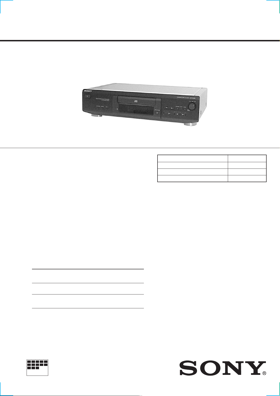
CDP-XE330
SERVICE MANUAL
AEP Model
UK Model
Model Name Using Similar Mechanism CDP-XE220/XE320
CD Mechanism Type CDM14FL-5BD29C
Base Unit Name BU-5BD29C
Optical Pick-up Name KSS-213BA/F-NP
SPECIFICATIONS
Compact Disc Player
Laser Semiconductor laser (λ = 780 nm)
Emission duration: continuous
Laser output Max 44.6 µW*
* This output is the value measured at a distance of
200 mm from the objective lens surface on the
Optical Pick-up block with 7 mm aperture.
Frequency response 2 Hz to 20 kHz ± 0.5 dB
Signal-to-noise ratio More than 100 dB
Dynamic range More than 92 dB
Harmonic distortion Less than 0.005%
Channel separation More than 95 dB
Output
Jack Maximum Load
type output impedance
level
LINE OUT Phono 2 V Over 10 kΩ
jacks (at 50 kΩ)
DIGITAL OUT Optical –18 dBm Wave length:
(OPTICAL) output 660 nm
connector
General
Power requirements 220 V – 230 V AC, 50/60 Hz
Power consumption 10W
Dimensions (approx.) 430 × 110 × 290 mm
(w/h/d) (17 × 4
Mass (approx.) 3.1 kg (6 lbs 14 oz)
Supplied accessories
Audio cord (2 phono plugs–2 phono plugs) (1)
Remote commander (remote) (1)
R6 (size AA) batteries (2)
Design and specifications are subject to change without notice.
3
/8 × 11 1/2 in.) incl. projecting parts
MICROFILM
COMPACT DISC PLAYER
Page 2
http://cxema.ru
SECTION 4
TEST MODE
4-1. AF MODE
The following checks can be performed in the AF mode, which is
set by connecting the TP2 (JW40 : AF ADJ) terminal on MAIN board
to the Ground and turning on the power.
• FL tube check
After all segments light up, when the · button is pressed
continuously, the follo wing will be displayed . (Partial lighting 1)
8 8 8
When the p button is pressed continuously , the following will be
displayed. (partial lighting 2)
24
6810
12 14
16 18 20
When the OPEN/CLOSE § button is pressed continuously, all
will light up again.
• Key check
All buttons have corresponding button numbers. When a button
is pressed, the counter will count up and display the button’s
number. Ho we ver, the counter will only count to “13”. It will not
count for buttons already pressed once, but will display the button’ s
number.
(Partial lighting 1)
(Partial lighting 2)
4-2. ADJ MODE
The following operations are performed in the ADJ mode, which
is set by connecting the TP3 (JW41 : ADJ) terminal to the Ground
and turning on the power.
FUNCTIONS OF NUMBER BUTTONS
(With the general remote commander)
Button
1
2
3
4
5
6
7
8
9
10
Focus bias adjustment plus (Not used in servicing)
EF-BALANCE adjustment plus (Not used in servicing)
Tracking servo off
Tracking gain adjusting plus (Not used in servicing)
Laser power control off (Not used in servicing)
Focus bias adjustment minus (Not used in servicing)
EF-BALANCE adjustment minus (Not used in servicing)
Tracking servo on
Tracking gain adjustment minus ((Not used in servicing)
Laser power control on (Not used in servicing)
Function
4-3. Aging Mode
This unit is equipped with an aging mode to check operations of the
mechanism deck.
• When faults occur:
Aging stops, and the state when aging stopped is displayed on the
fluorescent display tube.
• When no fault has occurred:
Aging is continued repeatedly.
888888
Â
Display of counting
Button
P
ENTER (AMS)
0
)
TIME
REPEAT
PLAY MODE
Button No.
Displayed
Display of button number
02
04
05
06
07
08
09
When the AMS knob is rotated to the right, the music calendar
changes from 1 n – – n 20 n 1.
When rotated to the left, it changes from 20 n 1 n 20 – –
• Remote commander check
When the · button of the remote commander is pressed, the
“·” lights up. All go off when the other buttons are pressed.
Â
Button
PEAK SERCH
CHECK
CLEAR
OPEN/
CLOSE §
PLAY ·
STOP p
Button No.
Displayed
10
11
12
All lit
Partial lighting 1
Partial lighting 2
Aging method 1
(When using the aging mode remote controller (J-2501-123-A)):
1. Press the U button and turn ON the power.
2. Set the disc on the tray.
3. Press the AGING STAR T button of the a ging remote controller.
4. Aging starts and the message shown in Fig. 1 is displayed on
the fluorescent display tube.
5. To end, press the U button.
Aging method 2 (When no aging mode remote controller):
1. Press the U button and turn ON the power.
2. Set the disc on the tray.
3. Press the ∏ button, CHECK button, and PLAY MODE
button together in this order.
4. Aging starts and the message shown in Fig. 1 is displayed on
the fluorescent display tube.
5. To end, press the U button.
Fig. 1 Message in Aging Mode
Code
No.
0
Load in
1
Access to TOC
2
Access to last track
3
Playback of last track
(3 seconds)
4
Access to first track
5
Playback of first track
(3 seconds)
6
Load out
State
Display when
normal
A0
A1
A2
Counter display
A4
Counter display
A6
Display when
abnormal
E0
E1
E2
E3
E4
E5
E6
— 6 —
Page 3
http://cxema.ru
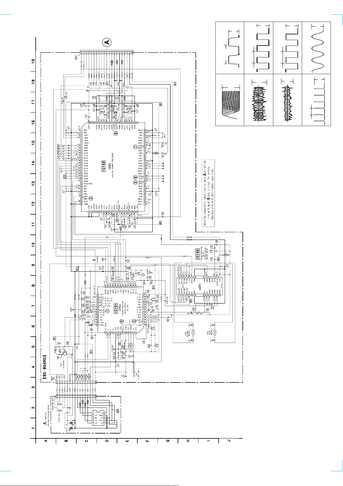
5Vp-p
5Vp-p
5Vp-p
2.6Vp-p
CDP-XE330
(Page 18)
• Waveform
230µsec
IC103 ^º XPCK
5
IC101 #£ RFO
1
1.3Vp-p
500mV/DIV, 500nsec/DIV
135µsec
IC103 ^™ RFCK
6
IC101 2 FEI
2
0.5Vp-p
200mV/DIV, 1µsec/DIV
135µsec
IC103 &¢ WFCK
7
IC101 $¶ TEI
3
0.2Vp-p
50mV/DIV, 1msec/DIV
16.9344MHz
IC103 *ª XTAI
8
2.5Vp-p
7.8µsec
IC103 @¶ MDP
4
• Refer to page 23 for IC Pin Functions.
• Refer to page 29 for IC Block Diagrams.
BA/F-NP
6-3. SCHEMATIC DIAGRAM — BD SECTION —
— 13 — — 14 —
16
Page 4
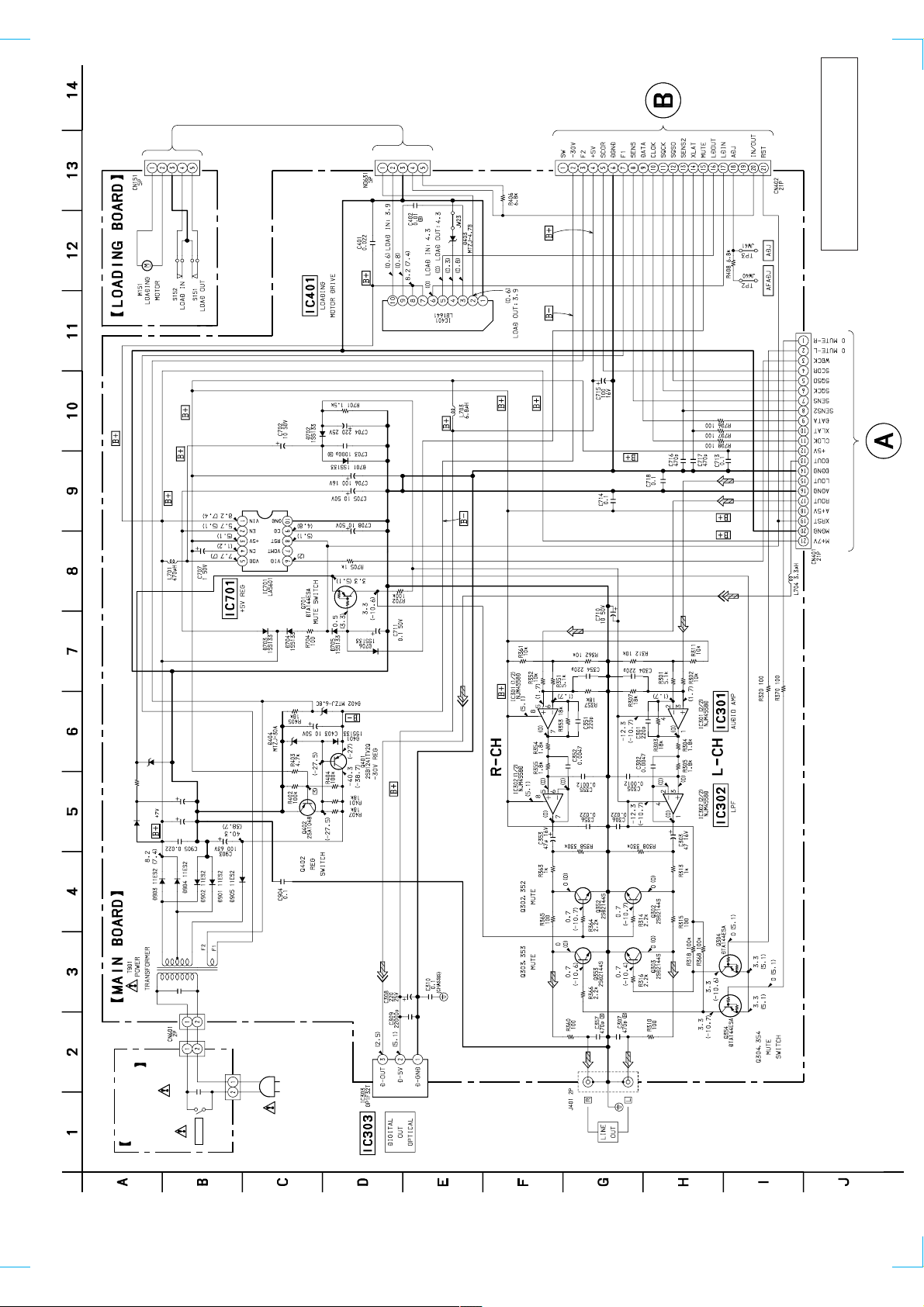
http://cxema.ru
CDP-XE330
(Page 21)
The components identified by mark ! or dotted
line with mark ! are critical for safety.
Replace only with part number specified.
(Page 14)
D910
MTZJ4.7B
R901
D906
330
1SS133
C909
C901
100µ 16V
6800µ 16V
— 17 — — 18 —
4700pF
C602
2P
CN603
C601
4700pF
2P
CN601
AC IN
~
16
BOARD
POWER SW
6-5. SCHEMATIC DIAGRAM — MAIN SECTION — • Refer to page 31 for IC Block Diagrams.
S601
POWER
Page 5
http://cxema.ru
CDP-XE330
• Waveform
IC501 #¡ EXTAL
1
4.2Vp-p
4MHz
R521
1k
DISPLAY BOARD
6-7. SCHEMATIC DIAGRAM — DISPLAY SECTION — • Refer to page 28 for IC Pin Functions.
2P
NO502
KEY BOARD
1
2
1
2
2P
NO301
16
(Page 18)
— 21 — — 22 —
Page 6
http://cxema.ru
The RF amplifier gain is determined by the resistance connected between this pin and RFO pin
External time constant setting pin during RF level control
APC amplifier output
APC amplifier input
RF I-V amplifier inverted input
Connect these pins to the photo diode A+C and B+D pins
Bias adjustment of focus error amplifier
Leave this pin open for automatic adjustment
F I-V and E I-V amplifier inverted input
Connect these pins to photo diodes F and E
I
I-V amplifier E gain adjustment
I
RF summing amplifier inverted input
I
IOIII
I
Pin Name I/O Function
RF M
RFTCLDPD
PD1
PD2
FE BIASFE
(When not using automatic balance adjustment)
Negative power supply
Tracking error amplifier output
E-F signal is output
Comparator input for balance adjustment
(Input from TEO through LPF)
Tracking error input
Window comparator input for ATSC detection
Trackig zero-cross comparator input
Capacitor connection pin for defect time constant
I
III
TEI
ATSC
IOI
TZC
TDFCTVCFZC
–
–
O
EI
VEE
TEO
LPFI
(VCC + VEE)/2 direct voltage output
Focus zero-cross comparator input
343536373839404142
Pin No.
Connected internally to the window comparator input for bias adjustment
Focus error input
Capacitor connection pin for defect time constant
Ground this pin through a capacitor for cutting the focus servo high-frequency gain
External time constant setting pin for boosting the focus servo low-frequency
Focus error amplifier output
O
I/O Function
III
Focus drive output
IOIIIII
Focus amplifier inverted input
External time constant setting pin for generating focus search waveform
43
44
45
46474849505152
APC : Auto Power Control
• Abbreviation
— 23 — — 24 —
External time constant setting pin for switching tracking high-frequency gain
External time constant setting pin for switching tracking high-frequency gain
Peak frequency setting pin for focus and tracking phase compensation amplifier
Tracking amplifier inverted input
Tracking drive output
Sled amplifier non-inverted input
Sled amplifier inverted input
Sled drive output
Connect an external capacitance to set the current which determines the Focus search, Track jump,
and Sled kick heights
Positive power supply
The sled overrun prevention circuit operates when this pin is Low (No pull-up resistance)
Serial data transfer clock input from CPU (No pull-up resistance)
Lach input from CPU (No pull-up resistance)
Serial data input from CPU (No pull-up resistance)
Reset input; resets at Low (No pull-up resistance)
Track number count signal output
Outputs FZC, DFCT1, TZC, BALH, TGH, FOH, ATSC, and others according to the command
from CPU
Outputs DFCT2, MIRR, BALL, TGL, FOL,and others according to the command from CPU
Focus OK comparator output
Input for the defect bottom hold output with capacitance coupled
Defect bottom hold output
Connected internally to the interruption comparator input
Connection pin for defect bottom hold capacitor
Connection pin for MIRR hold capacitor
MIRR comparator non-inverted input
Input for the RF summing amplifier output with capacitance coupled
RF summing amplifier output
Eye-pattern check point
IOI
I
I
O
IIIII
I
O
O
I
I
I
O
O
O
I
O
A TSC : Anti Shock
MIRR : Mirror
BALL : E-F Balance (Low)
TGL : Tracking Gain (Low)
FOL : Focus Bias (Low)
Pin Name
FEO
1
Pin No.
6-8. IC PIN FUNCTIONS
• IC101 FOCUS/TRACKING/SLED SERVO RF AMP (CXA1992AR)(BD board)
FEI
FDFCT
FGD
FLB
FE O
FE M
2345678
SRCH
TGU
TG2
FSET
9
10111213141516
TA M
TA O
SL P
SL M
SL O
ISET
VCC
LOCK
CLK
XLT
DAT A
XRST
C.OUT
SENS1
SENS2
FOK
CC2
171819202122232425
262728
CC1CBCP
29
30
RF I
313233
RF O
FZC : Focus zero-cross
DFCT : Defect
TZC : Tracking zero-cross
• Abbreviation
BALH: E-F Balance (High)
TGH : Tracking Gain (High)
FOH : Focus Bias (High)
Page 7

http://cxema.ru
• IC103 DIGITAL SIGNAL PROCESSOR (CXD2529Q)(BD board)
Pin No. Pin Name I/O Function
1
VDD
2
VSS
3
LMUT
4
RMUT
5
ACDT
6
CKOUT
7
SQCK
8
SQSO
9
SENS
10
11
12
13
14
15
16
17
18
19
20
21
22
23
24
25
26
27
28
29
30
31
32
33
34
35
36
37
38
39
40
DAT A
XLAT
CLOK
SEIN
CNIN
DATO
XLTO
CLKO
SPOA
SPOB
SPOC
SPOD
XLON
FOK
VDD
VSS
MON
MDP
MDS
LOCK
PWMI
TES0
TES1
VPCO2
VPCO1
VCKI
V16M
VCTL
PCO
FILO
FILI
–
+5V power supply
–
Ground
O
Lch “L” detection flog
O
Rch “L” detection flog
O
Test output (Not used)
O
Master clock divider output (Not used)
I
Clock input for SQSO read out
O
Serial output for Sub-Q 80bit
O
SENS signal output to CPU
I
Serial data input, supplied from CPU
I
Latch input, supplied from CPU
I
Serial data transfer clock input, supplied from CPU
I
SENS input from IC101
I
Numbers of track jump counted signal input
O
Serial data output to IC101
O
Serial data latch output to IC101
O
Serial data transfer clock output to IC101
I
Micro computer demodulation interface (Input A)
I
Micro computer demodulation interface (Input B)
I
Micro computer demodulation interface (Input C)
I
Micro computer demodulation interface (Input D)
O
Micro computer demodulation interface (Output)
I
Focus OK input
–
+5V power supply
–
Ground
O
Output to control ON/OFF of spindle motor (Not used)
O
Output to control spindle motor servo
O
Output to control spindle motor servo (Not used)
O
GFS is sampled by 460Hz
I
Input to control the outside spindle motor
I
Test pin (Connected to ground)
I
Test pin (Connected to ground)
O
Charge-pump output (Not used)
O
Charge-pump output (Not used)
I
VCO2 oscillator input (Not used)
O
VCO2 oscillator output (Not used)
I
VCO2 control voltage input
O
Charge-pump output to master PLL
O
Filter output to master PLL
I
Filter input for master PLL
• Abbreviation
GFS : Guarded Frame Sync
PLL :Phase Locked Loop
— 25 —
Page 8

http://cxema.ru
Pin No.
41
42
43
44
45
46
47
48
49
50
51
52
53
54
55
56
57
58
59
60
61
62
63
64
65
66
67
68
69
70
71
72
73
74
75
76
77
78
79
80
Pin Name I/O Function
AVSS
CLTV
AVDD
RF
BIAS
ASYI
ASYO
ASYE
WDCK
LRCK
LRCKI
PCMD
PCMDI
BCK
BCKI
VSS
VDD
GTOP
XUGF
XPLCK
GFS
RFCK
C2PO
XRAOF
MNT3
MNT1
MNT0
XTSL
FSTT
C4M
DOUT
EMPH
EMPHI
WFCK
SCOR
SBSO
EXCK
VSS
VDD
SYSM
–
Analog ground
I
Control voltage input for VCO
–
Analog power supply
I
EFM signal input
I
Asymmetry circuit constant current input
I
Asymmetry comparate voltage input
O
EFM full swing output (“L” =VSS, “H” =VDD)
I
Asymmetry circuit ON/OFF (“L”=OFF, “H”=ON)
O
D/A interface Word clock f=2fs
O
D/A interface LR clock output f=Fs
I
D/A interface LR clock input f=Fs
O
D/A interface Serial data output
I
D/A interface Serial data input
O
D/A interface Bit clock output
I
D/A interface Bit clock input
–
Ground
–
+5V power supply
O
Not used
O
Not used
O
EFM decoder PLL clock output
O
“H” Playback EFM sync and interpolation protection timming much
O
Read frame clock signal output
O
Not used
O
Internal RAM overflow detection signal output (Not used)
O
Not used
O
Not used
O
Not used
I
Not used
O
2/3 divider output (Not used)
O
4.2336MHz output(Not used)
O
Digital audio signal output
O
Playback disc output in emphasis mode
I
“H” =Input when de-emphasis ON
O
Write frame clock signal output
O
Sub-code sync output
O
Sub-P through Sub-W serial output
I
Clock input for SBSO read-out
–
Ground
–
+5V power supply
I
System mute input
• Abbreviation
EFM : Eight to Fourteen Modulation
— 26 —
Page 9

http://cxema.ru
—
AVSS
AVDD
AOUT1
AIN1
LOUT1
AVSS
XVDD
XTAI
XTAO
XVSS
AVSS
LOUT2
AIN2
AOUT2
AVDD
AVSS
—
—
XRST
Pin Name
–
–
–
O
O
–
–
O
–
–
O
O
–
–
–
–
Pin No. I/O
81
82
83
84
85
86
87
88
89
90
91
92
93
94
95
96
97
98
99
100
Not used
Analog ground
Analog power supply
Lch analog output
I
Lch opamp input
Lch line output
Analog ground
Master clock power supply
I
X’tal oscillator circuit input
X’tal oscillator circuit output
Master clock ground
Analog ground
Rch line output
I
Rch opamp input
Rch analog output
Analog power supply
Analog ground
Not used
Not used
I
System reset input
Function
— 27 —
Page 10

http://cxema.ru
• IC501 SYSTEM CONTROL ( CXP82616-034Q)(DISPLAY board)
Pin No. Pin Name I/O Function
1 GND – Ground
2 RMIN I Remote control signal input
3 GND – Ground
4 to 7 — – Not used
8 CLK O Serial clock output
9 SENSE I Sense signal input from IC103 (CXD2529Q)
10 DATA O Serial data output
11 SQCK O Sub Q clock output
12 SQSO I Sub Q data input
13 SENSE2 I Sense signal input from IC101 (CXA1992AR)
14 — – Not used (Open)
15 XLAT O Serial latch output
16 to 19 MUTE O Muting control signal output
20 LD OUT O Loading motor control
21 LD IN O Loading motor control
22, 23 — – Not used (Open)
24 to 26 KEY 0 to KEY 2 I Key input 0 to 2
27 — – Not used (Open)
28 ADJ/AFADJ I Test mode terminal
29 IN/OUT SW I CD tray IN/OUT switch
30 RST I System reset terminal
31 EXTAL O System oscillator (4.0 MHz)
32 XTAL I System oscillator (4.0 MHz)
33 VSS – Ground
34 to 41 OPEN – Not used (Open)
42 to 62 S21 to S1 O FL segment signal output
63 to 67 1G to 5G O FL grid signal output
68 — – Not used (Open)
69, 70 6G, 7G O FL grid signal output
71 VFDP (–30V) – Pull down voltage (–30V)
72 VDD (+5V) – Power supply (+5V)
73, 74 GND – Ground
75 VDD – Power supply (+5V)
76, 77 — – Not used (Open)
78 SCOR I Sub code data request signal input
79, 80 GND – Ground
• Abbreviation
FL : Fluorescent indicator tube
— 28 —
Page 11

http://cxema.ru
6-9. IC BLOCK DIAGRAMS
• CD section
IC101 CXA1992AR
PD2
–
FE_BIAS
LPFI
ATSC
TDFCT
+
PD2 IV
AMP
40
F
41
E
42
43
EI
44
VEE
TEO
45
46
47
TEI
48
49
TZC
50
51
VC
FZC
52
–
+
F IV AMP
–
+
E IV AMP
BAL1
BAL2
BAL3
BAL4
VEE
TOG4
TOG3
TOG2
TOG1
+
–
–
+
–
+
ATSC
WINDOW
COMP.
–
+
TZC COMP.
VCC
+
–
VCC
VEE
+
–
FZC COMP.
+
–
+
–
1
FEO
+
PD1 IV
AMP
TGFL
–
+
E-F BALANCE
WINDOW COMP.
PD1
–
VCC
VCC
IFB1
VEE
+
–
DFCT
TM1
2 3
FEI
IFB2
PD
+
APC
DFCT
FDFCT
VEE
–
IFB3
LD
+
–
+
–
VEE
LASER POWER CONTROL
FE AMP
IFB4
IFB5
IFB6
+
–
TRK. GAIN
WINDOW COMP.
+
–
TG1
FOCUS
PHASE COMPENSATION
FS4
4
FGD
VEE
MIRR
CP
–
+
VCC
–
+
–
–
+
RF_I
RF_O
+
–
FO. BIAS
WINDOW
COMP.
+
–
+
–
RF_M
–
+
RF SUMMING
AMP
+
–
+
–
+
–
–
+
VEE
LEVEL S
VCC
–
+
RFTC
+
–
FOK
LDON
LPCL
LPC
FOH
FOL
TGH
TGL
BALH
BALL
ATSC
TZC
FZC
TRACKING
PHASE COMPENSATION
TGFL
DFCTO
IIL DATA REGISTER
INPUT SHIFT REGISTER
ADDRESS DECODER
SENS SELECTOR
OUTPUT DECODER
IFB1-6
FS1-4 TG1-2 TM1-7 PS1-4
BAL1-4
TOG1-4
VCC
FS1
+
FS2
–
Charge
up
VEE
5 6 7 8 9 10
FLB
FE_O
FE_M
SRCH
TGU
FOK
CC1
CB
CC2
27282930313233343536373839
–
+
SENS2
26
+
–
IIL
↓
VCC
–
+
–
VEE
+
–
+
TTL
DFCT
+
MIRR
IIL
↓
TTL
DFCT1
CC1
TTL
↓
IIL
VCC
ISET
VCC VCC
SENS1
25
C. OUT
24
XRST
23
DATA
22
XLT
21
CLK
20
LOCK
19
VCC
18
ISET
17
SL_O
16
TM4 TM6
SL_M
15
TM7
TM3
FSET
TG2
TM5
–
SL_P
14
+
VEEVEE
TM2
–
+
131211
TG2
FSET
TA_M
TA_O
— 29 —
Page 12

http://cxema.ru
IC102 BA5941FP
IN4B
28
IN4A
IN3B
IN3A
OP OUT
OP IN (–)
OP IN (+)
27
26
24
25
22
23
GND
21 20
NC
VCC
OUT3A
18
19
OUT3B
1617
OUT4A
OUT4B
15
NC
+
–
Vcc
–
+
–
+
–
+
–
+
1 2
VCC
BIAS IN
IC103 CXD2529Q
80
3
IN1B
SYSM
79 78
VDD
–
+
–
+
+
–
+
–
VSS
4
IN1A
EXCK
77
5
SBSO
SCOR
76 75 74
IN2B
WFCK
73 72
6
EMPHI
IN2A
EMPH
71
DOUT
MUTE
FSTT
XTSL
MNT0
67
8
GND
MNT1
MNT3
66 65 64
7
GND
C4M
69 68
70
9
MUTE
XROF
63 62
C2PO
RFCK
VccVcc
10
VCC
GFS
61
LEVEL SHIFT
LEVEL SHIFT
LEVEL SHIFT
LEVEL SHIFT
+
+
GTOP
VDD
57
56 55 54
+
–
12 13
OUT2B
VSS
BCKI
–
11
OUT2A
XPCK
XUGF
59 58
60
BCK
PCMDI
535251
–
PCMD
OUT1A
LRCKI
+
–
14
OUT1B
AVSS
AVDD
AOUT1
AIN1
LOUT1
AVSS
XVDD
XTAI
XTAO
XVSS
AVSS
LOUT2
AIN2
AOUT2
AVDD
AVSS
XRST
OSC
50
LRCK
WDCK
49
48
ASYE
47
ASYO
46
ASYI
45
BIAS
44
RF
43
AVDD
42
CLTV
AVSS
41
40
FILI
FILO
39
38
PCO
37
VCTL
36
V16M
35
VCKI
VPCO1
34
33
VPCO2
32
TES1
31
TES0
81
NC
82
83
84
85
86
87
88
89
90
91
92
93
94
95
96
97
98
NC
99
NC
100
–
+
–
+
SERIAL-IN
INTERFACE
1 234
VDD
VSS
LMUT
OVER SAMPLING
TIMING
LOGIC
–
+
–
+
DIGITAL FILTER
56789 10
RMUT
TES2
CKOUT
PWMPWM
INTERFACE
SQCK
DEMODURATOR
3RD-ORDER NOISE SHAPER
SUB CODE
PROCESSOR
CPU
12 13
11
XLAT
SENS
DATA
SQSO
CLOK
SEIN
EFM
14
CNIN
SEQUENCER
15 16 17
XLTO
DATO
SERVO
AUTO
18 19
CLKO
SPOA
ERROR
CORRECTOR
16K RAM
21
20
SPOB
SPOC
SPOD
22 23
XLON
24
FOK
D / A
INTERFACE
DIGITAL OUT
25 26 27
VSS
VDD
DIGITAL CLV
28 29 30
MDP
MON
MDS
LOCK
PWMI
ASYMMETRY
CORRECTOR
DIGITAL
PLL
CLOCK
GENERATOR
— 30 —
Page 13

http://cxema.ru
• MAIN section
IC401 LB1641
PRE
DRIVER
INPUT LOGIC BLOCK
IC701 LA5601
21
GND OUT1 P1 VZ IN1 IN2 V
CD VIN
9
V REF
ON/OFF
AMP
RESET
6
VID VOD
VOMUTE
AMP
7
2 5
EN
CC
1VCC2 P2 OUT2
1
3
VO
8
RES
4
CN
10
GND
109876543
— 31 —
Page 14

http://cxema.ru
NOTE:
• -XX, -X mean standardized parts, so they may
have some differences from the original one.
• Items marked “*” are not stocked since they
are seldom required for routine service. Some
delay should be anticipated when ordering these
items.
7-1. MAIN SECTION
SECTION 7
EXPLODED VIEWS
• The mechanical parts with no reference number
in the exploded views are not supplied.
• Hardware (# mark) list and accessories and
packing materials are given in the last of this
parts list.
• Abbreviation
AED : North European
The components identified by mark ! or
dotted line with mark ! are critical for safety .
Replace only with part number specified.
13
14
#1
11
9
8
7
6
22
9
9
10
9
9
19
#1
15
13
9
UK model
21
20
3
not supplied
not supplied
#1
#1
#1
5
1
4
2
#1
12
#2
#2
not supplied
#1
T901
16
11
CDM14FL-5BD29C
Ref. No. Part No. Description Remarks Ref. No. Part No. Description Remarks
1 4-214-165-01 PANEL, LOADING
2 4-996-687-51 KNOB(AMS)
3 4-996-698-01 EMBLEM, SONY
4 3-354-981-11 SPRING (SUS), RING
5 4-977-593-11 RING(DIA. 50), ORNAMENTAL
6 X-4950-692-1 PANEL ASSY, FRONT
7 3-931-429-62 BUTTON (POWER)
* 8 1-672-315-11 POWER SW BOARD
9 4-951-620-01 SCREW(2.6 × 8), +BVTP
* 10 A-4724-499-A DISPLAY BOARD, COMPLETE
11 1-590-243-11 WIRE(FLAT TYPE) (21 CORE)
12 4-977-358-11 CUSHION
13 4-210-291-01 SCREW (CASE 3 TP2)
* 14 4-980-777-01 CASE (409526)
! 15 1-575-651-21 CORD, POWER
16 X-4947-207-1 FOOT ASSY (F50150S)
* 17 4-954-051-51 HOLDER, PC BOARD
* 18 A-4724-498-A MAIN BOARD, COMPLETE
* 19 4-214-171-02 PANEL, BACK(AEP,AED,CIS)
* 19 4-214-171-12 PANEL, BACK(UK)
20 4-966-267-11 BUSHING (FBS001), CORD
! 21 1-770-019-11 ADAPTOR, CONVERSION PLUG 3P(UK)
* 22 1-672-314-11 KEY BOARD
! T901 1-423-979-21 TRANSFORMER, POWER
#1
17
18
— 32 —
Page 15

http://cxema.ru
7-2. CD MECHANISM SECTION (CDM14FL-5BD29C)
NOTE: There are two types of MAGNET ASSY.
Confirm the shape before replacing the parts.
101
102
106
108
104
not supplied
115
107
105
103
#3
114
110
111
BU-5BD29C
113
110
111
112
Ref. No. Part No. Description Remarks Ref. No. Part No. Description Remarks
101 1-452-925-21 MAGNET ASSY
102 4-933-110-41 HOLDER (MG)
103 4-995-814-21 TABLE (FL), DISC
104 4-967-268-01 GEAR (C)
105 4-927-649-01 BELT
106 4-933-107-01 GEAR (PL)
107 4-927-651-01 PULLEY (S)
108 4-933-109-01 CAM
M151
109
109 1-645-721-11 LOADING BOARD
110 4-933-134-01 SCREW (+PTPWH M2.6 × 6)
111 4-959-996-01 SPRING (932), COMPRESSION
112 4-933-129-01 HOLDER (BU)
113 4-933-111-41 CHASSIS (MD)
114 4-917-583-21 BRACKET, YOKE
115 4-993-142-21 PULLEY (L), PRESS
M151 A-4604-363-A MOTOR (L) ASSY
— 33 —
Page 16

http://cxema.ru
7-3. BASE UNIT SECTION (BU-5BD29C)
151
152
153
158
155
154
M101
M102
154
156
157
#4
Ref. No. Part No. Description Remarks Ref. No. Part No. Description Remarks
! 151 8-848-379-31 OPTICAL PICK-UP KSS-213BA/F-NP
152 1-769-069-11 WIRE (FLAT TYPE) (16 CORE)
153 4-917-567-01 GEAR (M)
154 4-951-940-01 INSULATOR (BU)
155 4-917-565-01 SHAFT, SLED
156 4-917-564-01 GEAR (P), FLATNESS
* 157 A-4724-297-A BD BOARD, COMPLETE
158 3-713-786-51 SCREW +P 2 × 3
M101 X-4917-523-4 MOTOR ASSY(SPINDLE)
M102 X-4917-504-1 MOTOR ASSY(SLED)
The components identified by mark ! or dotted
line with mark ! are critical for safety.
Replace only with part number specified.
— 34 —
Page 17

http://cxema.ru
SECTION 8
ELECTRICAL PARTS LIST
BD
NOTE:
• Due to standardization, replacements in the
parts list may be different from the parts
specified in the diagrams or the components
used on the set.
• -XX, -X mean standardized parts, so they
may have some difference from the original
one.
• Items marked “*” are not stocked since they
are seldom required for routine service.
Some delay should be anticipated when
ordering these items.
Ref. No. Part No. Description Remarks Ref. No. Part No. Description Remarks
* A-4724-297-A BD BOARD, COMPLETE
******************
< CAPACITOR >
C101 1-126-607-11 ELECT CHIP 47uF 20% 4V
C102 1-163-141-00 CERAMIC CHIP 0.001uF 5% 50V
C103 1-164-346-11 CERAMIC CHIP 1uF 16V
C105 1-163-038-91 CERAMIC CHIP 0.1uF 25V
C106 1-164-161-11 CERAMIC CHIP 0.0022uF 10% 100V
C107 1-164-161-11 CERAMIC CHIP 0.0022uF 10% 100V
C108 1-163-021-91 CERAMIC CHIP 0.01uF 10% 50V
C109 1-163-021-91 CERAMIC CHIP 0.01uF 10% 50V
C110 1-163-989-11 CERAMIC CHIP 0.033uF 10% 25V
C111 1-163-017-00 CERAMIC CHIP 0.0047uF 5% 50V
C112 1-163-017-00 CERAMIC CHIP 0.0047uF 5% 50V
C113 1-164-161-11 CERAMIC CHIP 0.0022uF 10% 100V
C114 1-164-005-11 CERAMIC CHIP 0.47uF 25V
C115 1-126-607-11 ELECT CHIP 47uF 20% 4V
C116 1-163-016-00 CERAMIC CHIP 0.0039uF 10% 50V
C117 1-164-005-11 CERAMIC CHIP 0.47uF 25V
C118 1-164-004-11 CERAMIC CHIP 0.1uF 10% 25V
C119 1-163-038-91 CERAMIC CHIP 0.1uF 25V
C120 1-124-779-00 ELECT CHIP 10uF 20% 16V
C121 1-163-038-91 CERAMIC CHIP 0.1uF 25V
C122 1-163-021-91 CERAMIC CHIP 0.01uF 10% 50V
C123 1-163-038-91 CERAMIC CHIP 0.1uF 25V
C124 1-126-607-11 ELECT CHIP 47uF 20% 4V
C125 1-163-021-91 CERAMIC CHIP 0.01uF 10% 50V
C126 1-163-038-91 CERAMIC CHIP 0.1uF 25V
• CAPACITORS:
uF: µF
• RESISTORS
All resistors are in ohms.
METAL: metal-film resistor
METAL OXIDE: Metal Oxide-film resistor
F: nonflammable
• COILS
uH: µH
• Abbreviation
AED : North European
C175 1-163-038-91 CERAMIC CHIP 0.1uF 25V
C176 1-163-038-91 CERAMIC CHIP 0.1uF 25V
C177 1-163-038-91 CERAMIC CHIP 0.1uF 25V
C178 1-163-038-91 CERAMIC CHIP 0.1uF 25V
C179 1-163-038-91 CERAMIC CHIP 0.1uF 25V
C181 1-126-205-11 ELECT CHIP 47uF 20% 6.3V
C182 1-126-395-11 ELECT 22uF 20% 16V
C183 1-124-778-00 ELECT CHIP 22uF 20% 6.3V
C185 1-163-021-91 CERAMIC CHIP 0.01uF 10% 50V
C188 1-163-235-11 CERAMIC CHIP 22PF 5% 50V
C189 1-163-235-11 CERAMIC CHIP 22PF 5% 50V
CNU101 1-770-014-11 CONNECTOR, FFC/FPC 16P
CNU102 1-784-360-11 CONNECTOR,FFC(LIF(NON-ZIF))21P
FB101 1-414-234-22 INDUCTOR CHIP 0UH
FB103 1-414-234-22 INDUCTOR CHIP 0UH
IC101 8-752-080-62 IC CXA1992AR
IC102 8-759-429-32 IC BA5941FP-E2
IC103 8-752-380-64 IC CXD2529Q
JW101 1-216-295-91 SHORT 0
JW104 1-216-295-91 SHORT 0
• SEMICONDUCTORS
In each case, u: µ, for example:
uA...: µA... , uPA... , µPA... ,
uPB... , µPB... , uPC... , µPC... ,
uPD..., µPD...
When indicating parts by reference number,
please include the board name.
The components identified by mark ! or
dotted line with mark ! are critical for safety .
Replace only with part number specified.
< CONNECTOR >
< FERRITE BEAD >
< IC >
< JUMPER RESISTOR >
C127 1-164-161-11 CERAMIC CHIP 0.0022uF 10% 100V
C128 1-163-135-00 CERAMIC CHIP 560PF 5% 50V
C129 1-163-038-91 CERAMIC CHIP 0.1uF 25V
C130 1-164-336-11 CERAMIC CHIP 0.33uF 25V
C131 1-164-346-11 CERAMIC CHIP 1uF 16V
C140 1-110-501-11 CERAMIC CHIP 0.33uF 10% 16V
C154 1-163-235-11 CERAMIC CHIP 22PF 5% 50V
C161 1-164-005-11 CERAMIC CHIP 0.47uF 25V
C162 1-163-021-91 CERAMIC CHIP 0.01uF 10% 50V
C163 1-163-117-00 CERAMIC CHIP 100PF 5% 50V
C164 1-163-145-00 CERAMIC CHIP 0.0015uF 5% 50V
C165 1-164-004-11 CERAMIC CHIP 0.1uF 10% 25V
C166 1-163-137-00 CERAMIC CHIP 680PF 5% 50V
C167 1-163-121-00 CERAMIC CHIP 150PF 5% 50V
C168 1-163-137-00 CERAMIC CHIP 680PF 5% 50V
C169 1-163-121-00 CERAMIC CHIP 150PF 5% 50V
C170 1-163-233-11 CERAMIC CHIP 18PF 5% 50V
C171 1-163-237-11 CERAMIC CHIP 27PF 5% 50V
C173 1-163-038-91 CERAMIC CHIP 0.1uF 25V
C174 1-163-038-91 CERAMIC CHIP 0.1uF 25V
< TRANSISTOR >
Q101 8-729-010-08 TRANSISTOR MSB710-R
< RESISTOR >
R102 1-216-001-00 METAL CHIP 10 5% 1/10W
R104 1-216-093-91 RES,CHIP 68K 5% 1/10W
R105 1-216-088-00 METAL CHIP 43K 5% 1/10W
R106 1-216-088-00 METAL CHIP 43K 5% 1/10W
R107 1-216-088-00 METAL CHIP 43K 5% 1/10W
R108 1-216-088-00 METAL CHIP 43K 5% 1/10W
R109 1-216-093-91 RES,CHIP 68K 5% 1/10W
R114 1-216-101-00 METAL CHIP 150K 5% 1/10W
R115 1-216-101-00 METAL CHIP 150K 5% 1/10W
R116 1-216-061-00 METAL CHIP 3.3K 5% 1/10W
R117 1-216-069-00 METAL CHIP 6.8K 5% 1/10W
R118 1-216-063-91 RES,CHIP 3.9K 5% 1/10W
R119 1-216-085-00 METAL CHIP 33K 5% 1/10W
R120 1-216-089-91 RES,CHIP 47K 5% 1/10W
R121 1-216-114-00 RES,CHIP 510K 5% 1/10W
— 35 —
Page 18

http://cxema.ru
BD
Ref. No. Part No. Description Remarks Ref. No. Part No. Description Remarks
R122 1-216-097-91 RES,CHIP 100K 5% 1/10W
R123 1-216-099-00 METAL CHIP 120K 5% 1/10W
R124 1-216-091-00 METAL CHIP 56K 5% 1/10W
R125 1-216-069-00 METAL CHIP 6.8K 5% 1/10W
R126 1-216-063-91 RES,CHIP 3.9K 5% 1/10W
R127 1-216-089-91 RES,CHIP 47K 5% 1/10W
R128 1-216-098-00 METAL CHIP 110K 5% 1/10W
R129 1-216-049-91 RES,CHIP 1K 5% 1/10W
R130 1-216-079-00 METAL CHIP 18K 5% 1/10W
R131 1-216-079-00 METAL CHIP 18K 5% 1/10W
R132 1-216-061-00 METAL CHIP 3.3K 5% 1/10W
R133 1-216-061-00 METAL CHIP 3.3K 5% 1/10W
R134 1-216-065-91 RES,CHIP 4.7K 5% 1/10W
R135 1-216-065-91 RES,CHIP 4.7K 5% 1/10W
R136 1-216-073-00 METAL CHIP 10K 5% 1/10W
R137 1-216-065-91 RES,CHIP 4.7K 5% 1/10W
R138 1-216-025-91 RES,CHIP 100 5% 1/10W
R156 1-216-081-00 METAL CHIP 22K 5% 1/10W
R157 1-216-069-00 METAL CHIP 6.8K 5% 1/10W
R158 1-216-001-00 METAL CHIP 10 5% 1/10W
R159 1-216-121-91 RES,CHIP 1M 5% 1/10W
R161 1-216-097-91 RES,CHIP 100K 5% 1/10W
R162 1-216-073-00 METAL CHIP 10K 5% 1/10W
R163 1-216-121-91 RES,CHIP 1M 5% 1/10W
R164 1-216-061-00 METAL CHIP 3.3K 5% 1/10W
DISPLAY
* A-4724-499-A DISPLAY BOARD, COMPLETE
***********************
* 4-929-709-31 GUIDE(FL TUBE)
< CAPACITOR >
C501 1-161-494-00 CERAMIC 0.022uF 25V
C502 1-161-494-00 CERAMIC 0.022uF 25V
C503 1-164-159-11 CERAMIC 0.1uF 50V
C504 1-164-159-11 CERAMIC 0.1uF 50V
C506 1-124-584-00 ELECT 100uF 20% 10V
< CONNECTOR >
CN501 1-568-864-11 CONNECTOR, FFC 21P
< FLUORESCENT INDICATOR TUBE >
FL501 1-517-297-11 INDICATOR TUBE, FLUORESCENT
< IC >
IC501 8-752-880-56 IC CXP82616-034Q
IC502 8-749-014-66 IC NJL56H400A(REMOTE SENSOR)
< TRANSISTOR >
Q501 8-729-029-66 TRANSISTOR DTC114ESA
R165 1-216-049-91 RES,CHIP 1K 5% 1/10W
R166 1-216-073-00 METAL CHIP 10K 5% 1/10W
R167 1-216-683-11 METAL CHIP 22K 0.5% 1/10W
R168 1-216-073-00 METAL CHIP 10K 5% 1/10W
R169 1-216-079-00 METAL CHIP 18K 5% 1/10W
R170 1-216-683-11 METAL CHIP 22K 0.5% 1/10W
R171 1-216-073-00 METAL CHIP 10K 5% 1/10W
R172 1-216-079-00 METAL CHIP 18K 5% 1/10W
R173 1-216-049-91 RES,CHIP 1K 5% 1/10W
R174 1-216-033-00 METAL CHIP 220 5% 1/10W
R175 1-216-025-91 RES,CHIP 100 5% 1/10W
R176 1-216-049-91 RES,CHIP 1K 5% 1/10W
R177 1-216-049-91 RES,CHIP 1K 5% 1/10W
R178 1-216-049-91 RES,CHIP 1K 5% 1/10W
R179 1-216-025-91 RES,CHIP 100 5% 1/10W
R180 1-216-025-91 RES,CHIP 100 5% 1/10W
R181 1-216-025-91 RES,CHIP 100 5% 1/10W
R182 1-216-025-91 RES,CHIP 100 5% 1/10W
R183 1-216-025-91 RES,CHIP 100 5% 1/10W
R188 1-216-037-00 METAL CHIP 330 5% 1/10W
R189 1-216-025-91 RES,CHIP 100 5% 1/10W
R190 1-216-097-91 RES,CHIP 100K 5% 1/10W
R191 1-216-105-91 RES,CHIP 220K 5% 1/10W
< SWITCH >
S101 1-572-085-11 SWITCH, LEAF (LIMIT SW)
< VIBRATOR >
X101 1-767-408-21 VIBRATOR, CRYSTAL 16.9344 MHz
************************************************************
< RESISTOR >
R501 1-249-427-11 CARBON 6.8K 5% 1/4W F
R502 1-249-427-11 CARBON 6.8K 5% 1/4W F
R503 1-249-427-11 CARBON 6.8K 5% 1/4W F
R506 1-249-417-11 CARBON 1K 5% 1/4W F
R507 1-249-419-11 CARBON 1.5K 5% 1/4W F
R508 1-249-421-11 CARBON 2.2K 5% 1/4W F
R509 1-249-427-11 CARBON 6.8K 5% 1/4W F
R510 1-249-415-11 CARBON 680 5% 1/4W F
R511 1-249-417-11 CARBON 1K 5% 1/4W F
R512 1-249-419-11 CARBON 1.5K 5% 1/4W F
R513 1-249-427-11 CARBON 6.8K 5% 1/4W F
R514 1-249-415-11 CARBON 680 5% 1/4W F
R515 1-247-807-31 CARBON 100 5% 1/4W
R516 1-249-441-11 CARBON 100K 5% 1/4W
R517 1-247-843-11 CARBON 3.3K 5% 1/4W
R518 1-249-427-11 CARBON 6.8K 5% 1/4W F
R519 1-249-431-11 CARBON 15K 5% 1/4W
R520 1-247-807-31 CARBON 100 5% 1/4W
R521 1-249-417-11 CARBON 1K 5% 1/4W F
< SWITCH >
S508 1-762-752-11 SWITCH, TACTILE(PEAK SEARCH)
S509 1-762-752-11 SWITCH, TACTILE(CHECK)
S510 1-762-752-11 SWITCH, TACTILE(CLEAR)
S511 1-762-752-11 SWITCH, TACTILE(OPEN/CLOSE)
S512 1-762-752-11 SWITCH, TACTILE(·)
S513 1-762-752-11 SWITCH, TACTILE(P)
S514 1-762-752-11 SWITCH, TACTILE(p)
S515 1-762-752-11 SWITCH, TACTILE())
S516 1-762-752-11 SWITCH, TACTILE(0)
S520 1-475-543-11 ENCODER, ROTARY(AMS)
< VIBRATOR >
X501 1-577-082-11 VIBRATOR, CERAMIC 4.0MHz
************************************************************
— 36 —
Page 19

http://cxema.ru
KEY LOADING
Ref. No. Part No. Description Remarks Ref. No. Part No. Description Remarks
* 1-672-314-11 KEY BOARD
*********
< RESISTOR >
R504 1-249-415-11 CARBON 680 5% 1/4W F
R505 1-249-417-11 CARBON 1K 5% 1/4W F
< SWITCH >
S502 1-762-752-11 SWITCH, TACTILE(TIME)
S503 1-762-752-11 SWITCH, TACTILE(REPEAT)
S504 1-762-752-11 SWITCH, TACTILE(PLAY MODE)
************************************************************
1-645-721-11 LOADING BOARD
*************
< CONNECTOR >
C713 1-164-159-11 CERAMIC 0.1uF 50V
C714 1-164-159-11 CERAMIC 0.1uF 50V
C715 1-126-933-11 ELECT 100uF 20% 16V
C716 1-162-290-31 CERAMIC 470PF 10% 50V
C717 1-162-290-31 CERAMIC 470PF 10% 50V
C718 1-164-159-11 CERAMIC 0.1uF 50V
C901 1-128-547-11 ELECT 6800uF 20% 16V
C903 1-128-576-11 ELECT 100uF 20% 63V
C904 1-164-159-11 CERAMIC 0.1uF 50V
C905 1-161-494-00 CERAMIC 0.022uF 25V
C909 1-126-933-11 ELECT 100uF 20% 16V
< CONNECTOR >
CN401 1-784-782-11 CONNECTOR, FFC 21P
CN402 1-784-782-11 CONNECTOR, FFC 21P
CN602 1-564-321-00 PIN, CONNECTOR 2P
MAIN
* CN151 1-568-943-11 PIN, CONNECTOR 5P
< SWITCH >
S151 1-572-086-11 SWITCH, LEAF(LOAD OUT)
S152 1-572-086-11 SWITCH, LEAF(LOAD IN)
************************************************************
* A-4724-498-A MAIN BOARD, COMPLETE
********************
< CAPACITOR >
C301 1-162-286-31 CERAMIC 220PF 10% 50V
C302 1-130-479-00 MYLAR 0.0047uF 5% 50V
C303 1-104-664-11 ELECT 47uF 20% 16V
C304 1-162-286-31 CERAMIC 220PF 10% 50V
C305 1-130-472-00 MYLAR 0.0012uF 5% 50V
C306 1-161-494-00 CERAMIC 0.022uF 25V
C307 1-162-290-31 CERAMIC 470PF 10% 50V
C308 1-104-666-11 ELECT 220uF 20% 25V
C309 1-161-494-00 CERAMIC 0.022uF 25V
C310 1-164-159-11 CERAMIC 0.1uF 50V
C351 1-162-286-31 CERAMIC 220PF 10% 50V
C352 1-130-479-00 MYLAR 0.0047uF 5% 50V
C353 1-104-664-11 ELECT 47uF 20% 16V
C354 1-162-286-31 CERAMIC 220PF 10% 50V
C355 1-130-472-00 MYLAR 0.0012uF 5% 50V
C356 1-161-494-00 CERAMIC 0.022uF 25V
C357 1-162-290-31 CERAMIC 470PF 10% 50V
C401 1-161-494-00 CERAMIC 0.022uF 25V
C402 1-162-306-11 CERAMIC 0.01uF 20% 16V
C403 1-126-964-11 ELECT 10uF 20% 50V
< DIODE >
D401 8-719-911-19 DIODE 1SS119
D402 8-719-109-97 DIODE RD6.8ES-B2
D403 8-719-921-40 DIODE MTZJ-4.7C
D404 8-719-982-19 DIODE MTZJ-30A
D701 8-719-911-19 DIODE 1SS119
D702 8-719-911-19 DIODE 1SS119
D703 8-719-911-19 DIODE 1SS119
D704 8-719-911-19 DIODE 1SS119
D705 8-719-911-19 DIODE 1SS119
D706 8-719-911-19 DIODE 1SS119
D901 8-719-024-99 DIODE 11ES2-NTA2B
D902 8-719-024-99 DIODE 11ES2-NTA2B
D903 8-719-024-99 DIODE 11ES2-NTA2B
D904 8-719-024-99 DIODE 11ES2-NTA2B
D905 8-719-024-99 DIODE 11ES2-NTA2B
D906 8-719-911-19 DIODE 1SS119
D910 8-719-921-40 DIODE MTZJ-4.7C
< TERMINAL >
* EB1 1-537-738-21 TERMINAL, EARTH
< IC >
IC301 8-759-634-51 IC M5218AP
IC302 8-759-634-51 IC M5218AP
IC303 8-749-921-12 IC GP1F32T(DIGITAL OUT)
IC401 8-759-822-09 IC LB1641
IC701 8-759-821-93 IC LA5601
< JACK >
C602 1-113-924-11 CERAMIC 0.0047uF 20% 250V
C702 1-126-964-11 ELECT 10uF 20% 50V
C703 1-162-294-31 CERAMIC 0.001uF 10% 50V
C704 1-104-666-11 ELECT 220uF 20% 25V
C705 1-126-964-11 ELECT 10uF 20% 50V
C706 1-126-933-11 ELECT 100uF 20% 16V
C707 1-126-960-11 ELECT 1uF 20% 50V
C708 1-126-964-11 ELECT 10uF 20% 50V
C710 1-126-964-11 ELECT 10uF 20% 50V
C711 1-164-159-11 CERAMIC 0.1uF 50V
J401 1-785-868-11 JACK, PIN 2P(LINE OUT)
< COIL >
L701 1-414-223-11 INDUCTOR 470uH
L703 1-410-507-11 INDUCTOR 6.8uH
L704 1-410-322-11 INDUCTOR 3.3uH
< TRANSISTOR >
Q302 8-729-922-37 TRANSISTOR 2SD2144S
Q303 8-729-922-37 TRANSISTOR 2SD2144S
Q304 8-729-029-56 TRANSISTOR DTA144ESA
Q352 8-729-922-37 TRANSISTOR 2SD2144S
Q353 8-729-922-37 TRANSISTOR 2SD2144S
— 37 —
Page 20

http://cxema.ru
CDP-XE330
MAIN
Ref. No. Part No. Description Remarks Ref. No. Part No. Description Remarks
Q354 8-729-029-56 TRANSISTOR DTA144ESA
Q401 8-729-041-38 TRANSISTOR 2SB1241TV2Q
Q402 8-729-119-76 TRANSISTOR 2SA1175-HFE
Q701 8-729-029-56 TRANSISTOR DTA144ESA
R301 1-247-848-11 CARBON 5.1K 5% 1/4W
R302 1-249-429-11 CARBON 10K 5% 1/4W
R303 1-249-432-11 CARBON 18K 5% 1/4W
R304 1-249-420-11 CARBON 1.8K 5% 1/4W F
R305 1-249-420-11 CARBON 1.8K 5% 1/4W F
R307 1-249-432-11 CARBON 18K 5% 1/4W
R308 1-247-891-00 CARBON 330K 5% 1/4W
R310 1-247-807-31 CARBON 100 5% 1/4W
R311 1-249-429-11 CARBON 10K 5% 1/4W
R312 1-249-429-11 CARBON 10K 5% 1/4W
R313 1-249-417-11 CARBON 1K 5% 1/4W F
R314 1-249-421-11 CARBON 2.2K 5% 1/4W F
R315 1-247-807-31 CARBON 100 5% 1/4W
R316 1-249-421-11 CARBON 2.2K 5% 1/4W F
R318 1-249-441-11 CARBON 100K 5% 1/4W
R320 1-247-807-31 CARBON 100 5% 1/4W
R351 1-247-848-11 CARBON 5.1K 5% 1/4W
R352 1-249-429-11 CARBON 10K 5% 1/4W
R353 1-249-432-11 CARBON 18K 5% 1/4W
R354 1-249-420-11 CARBON 1.8K 5% 1/4W F
POWER SW
< RESISTOR >
* 1-672-315-11 POWER SW BOARD
***************
< CAPACITOR >
! C601 1-113-924-11 CERAMIC 0.0047uF 20% 250V
< CONNECTOR >
* CN601 1-580-230-31 PIN, CONNECTOR (PC BOARD) 2P
CN603 1-769-745-71 LEAD (WITH CONNECTOR) (2 CORE)
< SWITCH >
! S601 1-572-267-51 SWITCH, PUSH (AC POWER)(1 KEY)(POWER)
************************************************************
MISCELLANEOUS
*************
11 1-590-243-11 WIRE(FLAT TYPE) (21 CORE)
! 15 1-575-651-21 CORD, POWER
! 21 1-770-019-11 ADAPTOR, CONVERSION PLUG 3P(UK)
101 1-452-925-21 MAGNET ASSY
! 151 8-848-379-31 OPTICAL PICK-UP KSS-213BA/F-NP
152 1-769-069-11 WIRE (FLAT TYPE) (16 CORE)
M101 X-4917-523-4 MOTOR ASSY(SPINDLE)
M102 X-4917-504-1 MOTOR ASSY(SLED)
M151 A-4604-363-A MOTOR (L) ASSY
R355 1-249-420-11 CARBON 1.8K 5% 1/4W F
R357 1-249-432-11 CARBON 18K 5% 1/4W
R358 1-247-891-00 CARBON 330K 5% 1/4W
R360 1-247-807-31 CARBON 100 5% 1/4W
R361 1-249-429-11 CARBON 10K 5% 1/4W
R362 1-249-429-11 CARBON 10K 5% 1/4W
R363 1-249-417-11 CARBON 1K 5% 1/4W F
R364 1-249-421-11 CARBON 2.2K 5% 1/4W F
R365 1-247-807-31 CARBON 100 5% 1/4W
R366 1-249-421-11 CARBON 2.2K 5% 1/4W F
R368 1-249-441-11 CARBON 100K 5% 1/4W
R370 1-247-807-31 CARBON 100 5% 1/4W
R401 1-249-432-11 CARBON 18K 5% 1/4W
R402 1-249-441-11 CARBON 100K 5% 1/4W
R403 1-249-425-11 CARBON 4.7K 5% 1/4W F
R404 1-249-441-11 CARBON 100K 5% 1/4W
R405 1-249-432-11 CARBON 18K 5% 1/4W
R406 1-249-427-11 CARBON 6.8K 5% 1/4W F
R407 1-249-432-11 CARBON 18K 5% 1/4W
R408 1-249-427-11 CARBON 6.8K 5% 1/4W F
R701 1-249-419-11 CARBON 1.5K 5% 1/4W F
R702 1-249-441-11 CARBON 100K 5% 1/4W
R704 1-247-807-31 CARBON 100 5% 1/4W
R705 1-249-417-11 CARBON 1K 5% 1/4W F
R706 1-247-807-31 CARBON 100 5% 1/4W
************************************************************
ACCESSORIES & PACKING MATERIALS
*******************************
1-467-880-11 REMOTE COMMANDER (RM-D420)
1-776-263-11 CORD,CONNECTION (AUDIO)
3-865-462-11 MANUAL, INSTRUCTION
(ENGLISH/FRENCH/SPANISH)(AEP/UK)
3-865-462-21 MANUAL, INSTRUCTION
(GERMAN/DUTCH/ITALIAN/PORTUGUESE)(AEP)
3-865-462-31 MANUAL, INSTRUCTION
(SWEDISH/DANISH/FINNISH)(AED)
3-865-462-41 MANUAL, INSTRUCTION
(ENGLISH/POLISH/RUSSIAN)(CIS)
3-865-462-51 MANUAL, INSTRUCTION(HUNGARIAN)(CIS)
3-865-462-61 MANUAL, INSTRUCTION(CZECH)(CIS)
3-865-462-71 MANUAL, INSTRUCTION(TURKISH)(CIS)
3-865-462-81 MANUAL, INSTRUCTION(GREEK)(CIS)
4-962-615-01 COVER, BATTERY (For RM-D420)
************************************************************
*************
HARDWARE LIST
*************
R707 1-247-807-31 CARBON 100 5% 1/4W
R708 1-247-807-31 CARBON 100 5% 1/4W
R901 1-249-411-11 CARBON 330 5% 1/4W
< TRANSFORMER >
! T901 1-423-979-21 TRANSFORMER, POWER
************************************************************
9-928-850-11
#1 7-685-646-79 SCREW +BVTP 3 × 8 TYPE2 N-S
#2 7-685-649-79 SCREW +BVTP 3 × 14 TYPE2 IT-3
#3 7-621-775-10 SCREW +B 2.6 × 4
#4 7-685-134-19 SCREW +BTP 2.6 × 8 TYPE2 N-S
Sony Corporation
Home A&V Products Company
— 38 —
The components identified by mark ! or dotted
line with mark ! are critical for safety.
Replace only with part number specified.
99D167549-1
Printed in Hungary ©1999.4
Published by Quality Assurance Dept.
(Shinagawa)
 Loading...