Sony CDPXA-555-ES Service manual
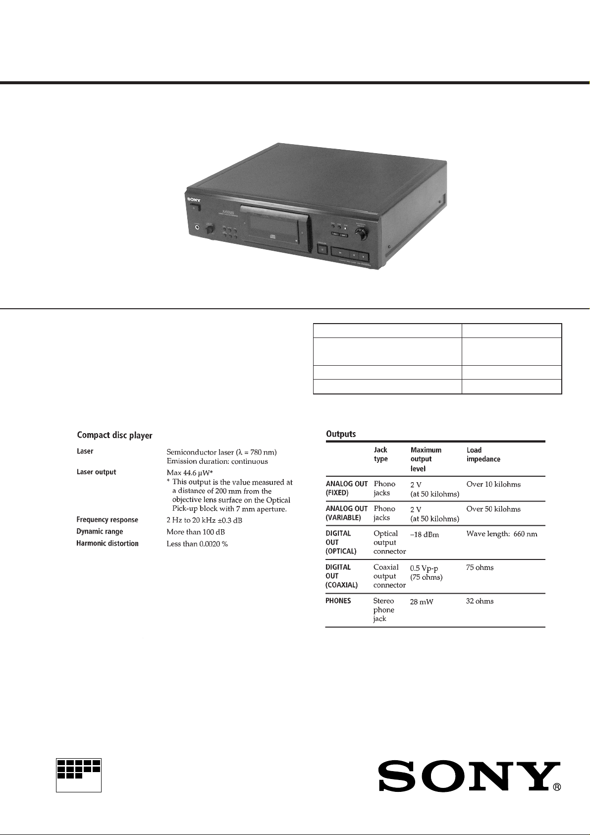
CDP-XA555ES
SERVICE MANUAL
Photo: Black
AEP Model
E Model
Model Name Using Similar Mechanism CDP-XA50ES
CD Mechanism Type
Base Unit Type BU-12C
Optical Pick-up Type KSS-273B/J1N
CDM32EB-12C (BLACK)
CDM32EN-12C (GOLD)
SPECIFICATIONS
– Continued on next page –
MICROFILM
COMPACT DISC PLAYER
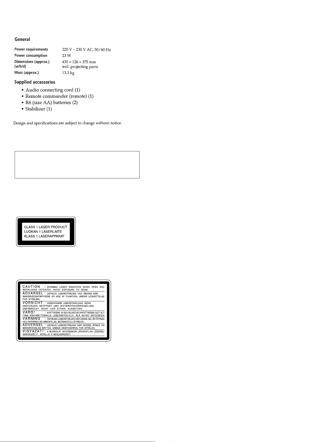
CAUTION
Use of controls or adjustments or performance of procedures
other than those specified herein may result in hazardous radiation exposure.
This appliance is classified as a CLASS 1 LASER product.
The CLASS 1 LASER PRODUCT MARKING is located on
the rear exterior.
Laser component in this product is capable of emitting radiation
exceeding the limit for Class 1.
The following caution label is located inside the unit.
TABLE OF CONTENTS
1. SERVICING NOTES ............................................... 3
2. GENERAL ................................................................... 6
3. DISASSEMBLY ......................................................... 8
4. TEST MODE.............................................................. 11
5. ELECTRICAL ADJUSTMENTS......................... 13
6. DIAGRAMS
6-1. Block Diagram – SERVO Section –.............................. 15
6-2. Block Diagram – MAIN Section –................................ 16
6-3. Notes for Printed Wiring Board
and Schematic Diagram .................................................. 17
6-4. Printed Wiring Board
– SERVO Board (Component Side) – ............................ 18
6-5. Printed Wiring Board
– SERVO Board (Conductor Side) – .............................. 19
6-6. Schematic Diagram – SERVO Board (1/2) – ................. 20
6-7. Schematic Diagram – SERVO Board (2/2) – ................. 21
6-8. Printed Wiring Boards
– BSL/FL RELAY/FLEX RELAY/
LOADING MOTOR/LOADING SW Boards – ............. 22
6-9. Schematic Diagram
– BSL/FL RELAY/FLEX RELAY/
LOADING MOTOR/LOADING SW Boards – ............. 23
6-10. Printed Wiring Board
– AUDIO Board (Component Side) – ............................ 24
6-11. Printed Wiring Board
– AUDIO Board (Conductor Side) – .............................. 25
6-12. Schematic Diagram – AUDIO Board (1/2) – ................. 26
6-13. Schematic Diagram – AUDIO Board (2/2) – ................. 27
6-14. Printed Wiring Boards – COAX OUT/
D/O SW/LINE/OPT OUT/VR Boards – ........................ 28
6-15. Schematic Diagram – COAX OUT/
D/O SW/LINE/OPT OUT/VR Boards – ........................ 29
6-16. Printed Wiring Boards – KEY-L/KEY-R Boards –....... 30
6-17. Schematic Diagram – KEY-L/KEY-R Boards – ........... 31
6-18. Printed Wiring Board – DISPLAY Board – .................. 32
6-19. Schematic Diagram – DISPLAY Board – ..................... 33
6-20. Printed Wiring Boards
– AC/POWER (Component Side)/SW Boards –............ 34
6-21. Printed Wiring Board
– POWER Board (Conductor Side) –............................. 35
6-22. Schematic Diagram – AC/POWER/SW Boards – ........ 36
6-23. IC Pin Function Description ........................................... 42
SAFETY-RELATED COMPONENT WARNING!!
COMPONENTS IDENTIFIED BY MARK 0 OR DOTTED
LINE WITH MARK 0 ON THE SCHEMATIC DIAGRAMS
AND IN THE PARTS LIST ARE CRITICAL TO SAFE
OPERATION. REPLACE THESE COMPONENTS WITH
SONY PARTS WHOSE PART NUMBERS APPEAR AS
SHOWN IN THIS MANUAL OR IN SUPPLEMENTS PUBLISHED BY SONY.
2
7. EXPLODED VIEWS ................................................ 48
8. ELECTRICAL PARTS LIST ............................... 55
Notes on chip component replacement
• Never reuse a disconnected chip component.
• Notice that the minus side of a tantalum capacitor may be dam-
aged by heat.
Flexible Circuit Board Repairing
• Keep the temperature of the soldering iron around 270 ˚C dur-
ing repairing.
• Do not touch the soldering iron on the same conductor of the
circuit board (within 3 times).
• Be careful not to apply force on the conductor when soldering
or unsoldering.
SECTION 1
SERVICING NOTES
NOTES ON HANDLING THE OPTICAL PICK-UP
BLOCK OR BASE UNIT
The laser diode in the optical pick-up block may suffer electrostatic break-down because of the potential difference generated
by the charged electrostatic load, etc. on clothing and the human
body.
During repair, pay attention to electrostatic break-down and also
use the procedure in the printed matter which is included in the
repair parts.
The flexible board is easily damaged and should be handled with
care.
NOTES ON LASER DIODE EMISSION CHECK
The laser beam on this model is concentrated so as to be focused
on the disc reflective surface by the objective lens in the optical
pick-up block. Therefore, when checking the laser diode emission, observe from more than 30 cm away from the objective lens.
MODEL IDENTIFICATION
– BACK PANEL –
4-221-269-
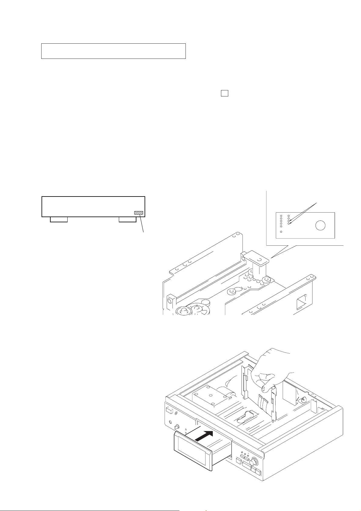
HOW TO PLAY CD WITH THE DISC TRAY
OPENED
To play a CD by this method, the screws that secure the SERVO
board to the chassis must be removed in advance.
Procedure:
1. Press ! button to turn the power ON.
2. Set a CD on the disc tray.
3. W ith the disc tray opened, connect pin 1 and pin 2 of CN272
on the LOADING MOTOR board using tweezers, etc.
4. As the disc starts to move toward direction A, intercept the
sensor in B section with your finger immediately . (See “HOW
TO OPERATE THE SET WITHOUT USING STABILIZER”
on page 5)
5. You can release your hand when TOC is read.
6. Hence, the operation equivalent to normal operation can be
performed.
short here
AEP Model : 0
Singapore Model: 1
s
s
B
A
3
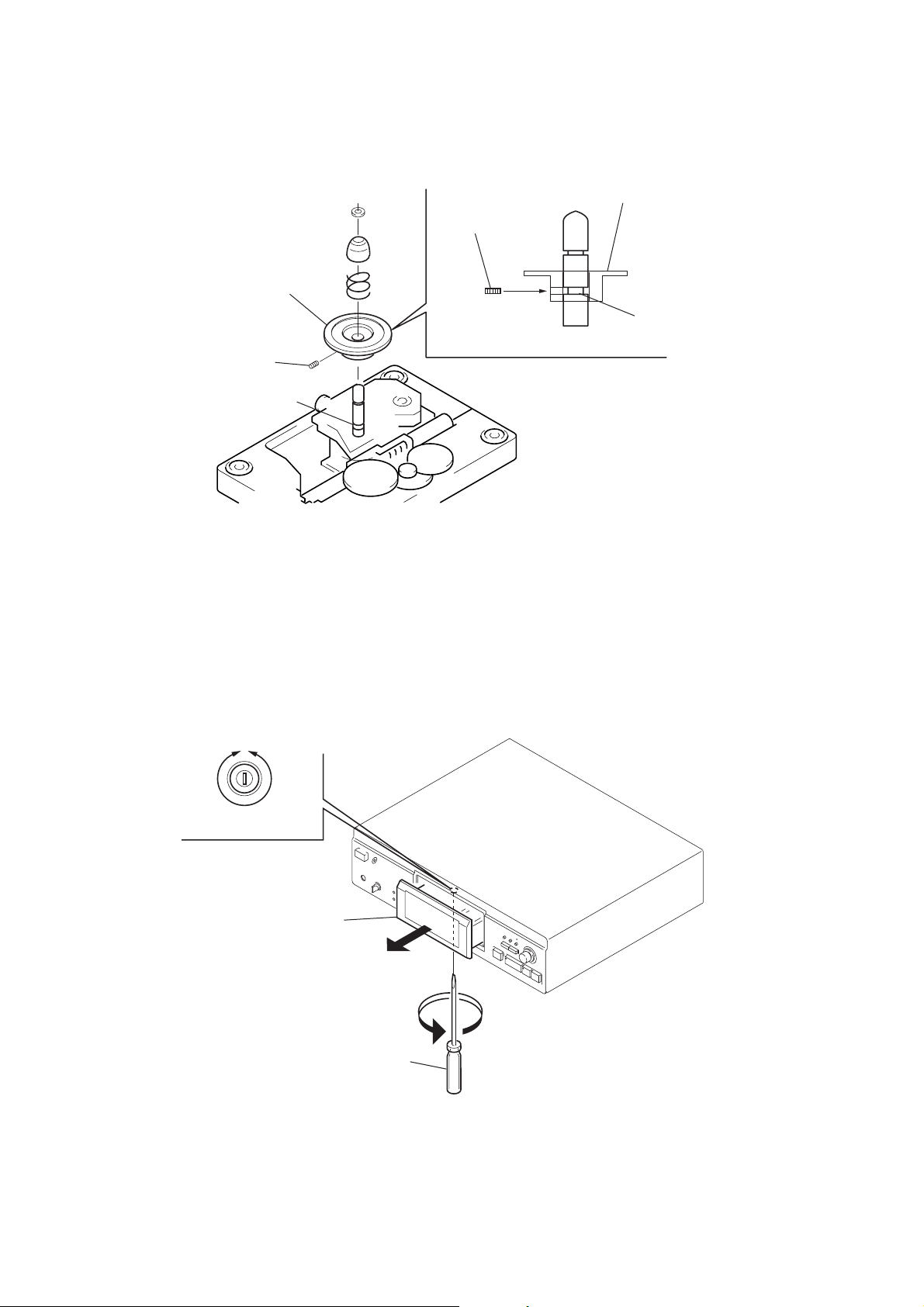
DISC PULLEY INSTALLING POSITION
Note: The shaft on which the disc pulley is installed has a groove to determine the position (height).
Install the disc pulley so that a setscrew can settle in this groove.
set screw
disc pulley
set screw
×
4)
(M2.6
groove
disc pulley
groove
HOW TO OPEN DISC TRAY WHEN POWER IS OFF
Insert a flat-blade screwdriver into a hole at the bottom of the set, and rotate the pulley in the arrow direction to open the disc tray.
OUT
IN
disc tray
flat-blade
screwdriver
4
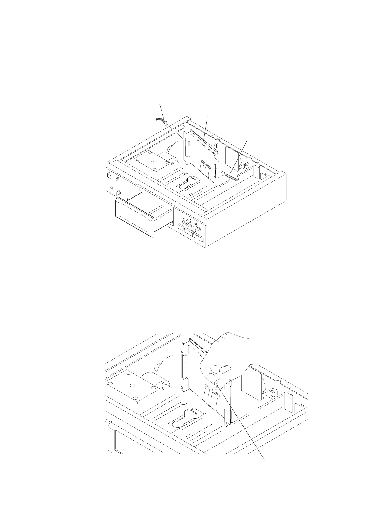
SERVICE POSITION OF SERVO BOARD
In servicing the SERVO board, erect the board as shown below.
In this case, the CN201 and CN202 connectors are disconnected respectively, and accordingly the buttons on the front panel do not
function.
Therefore, use the Remote Commander for fundamental operations such as PLAY and STOP.
Also, in performing the service under this condition, the stabilizer is not detected, so refer to “How to Operate the Set without Using
Stabilizer”.
disconnect CN201
SERVO board
disconnect CN202
HOW TO OPERATE THE SET WITHOUT USING STABILIZER
As this set detects the stabilizer, if servicing the set in other than normal operating way, disable the stabilizer detecting function by the
following method.
The stabilizer is detected before TOC is read, and after that, this function does not operate.
That is, the stabilizer detection is executed after power on or immediately after disc loading, and you can release your finger after the disc
was recognized.
Intercept the D202 on SERVO board
with your finger.
5
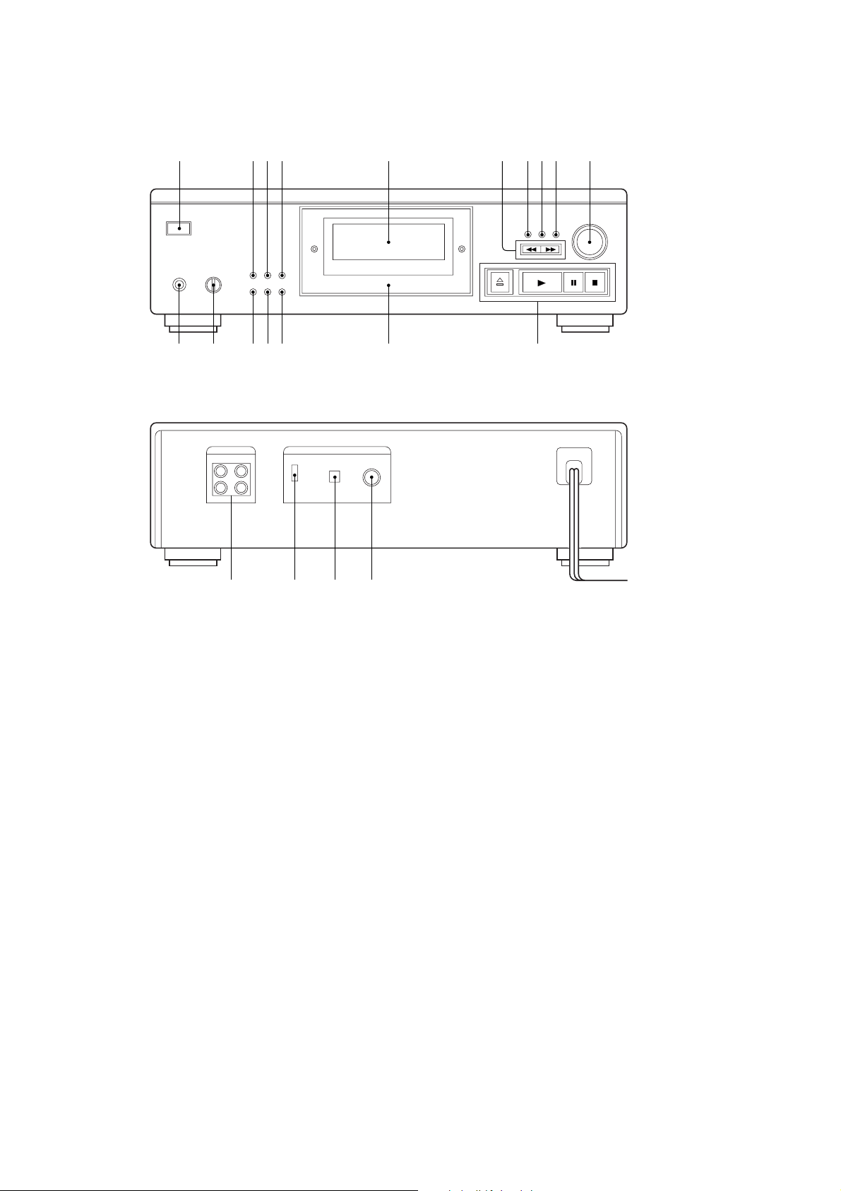
LOCATION OF CONTROLS
Front view
SECTION 2
GENERAL
Rear view
1 234 5 0
qdqfqgqhqj
76 89
qaqs
qk ql
1 ! (power) switch
2 PLAY MODE button
3 REPEAT button
4 TIME button
5 Fluorescent indicator tube display
6 m/M (forward/backward) button
7 CHECK button
8 CLEAR button
9 FILTER button and indicator
0 AMS control
qa x (stop) button
X (pause) button and indicator
N (play) button and indicator
A OPEN/CLOSE button
w; wa
qs Disc table
qd ERASE button
qf FILE button
qg EDIT/TIME FADE button
qh LINE OUT/PHONE LEVEL volume
qj PHONES jack
qk ANALOG OUT (FIXED/VARIABLE) connector
ql DIGITAL OUT ON/OFF switch
w; DIGITAL OUT (OPTICAL) connector
wa DIGITAL OUT (COAXIAL) connector
6
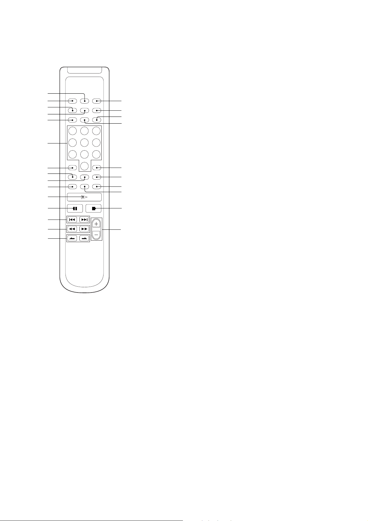
Remote commander
1
2
3
4
5
1 2 3
6
7
8
9
0
qa
qs
qd
qf
qg
4 5 6
7 8 9
10
qh
qj
qk
ql
w;
wa
ws
wd
wg
wf
1 SHUFFLE button
2 CONTINUE button
3 C.INDEX button
4 A.SPACE button
5 TIME button
6 Number button
7 >10 button
8 FILE button
9 ERASE button
0 REPEAT button
qa H (play) button
qs X (pause) button
qd ./> (AMS) button
qf m/M (forward/backward) button
qg INDEX >/. button
qh PROGRAM button
qj PEAK SEARCH button
qk DIGITAL FILTER button
ql DISPLAY MODE button
w; CLEAR button
wa CHECK button
ws FADER button
wd A Tt B button
wf x (stop) button
wg LINE OUT LEVEL button
7
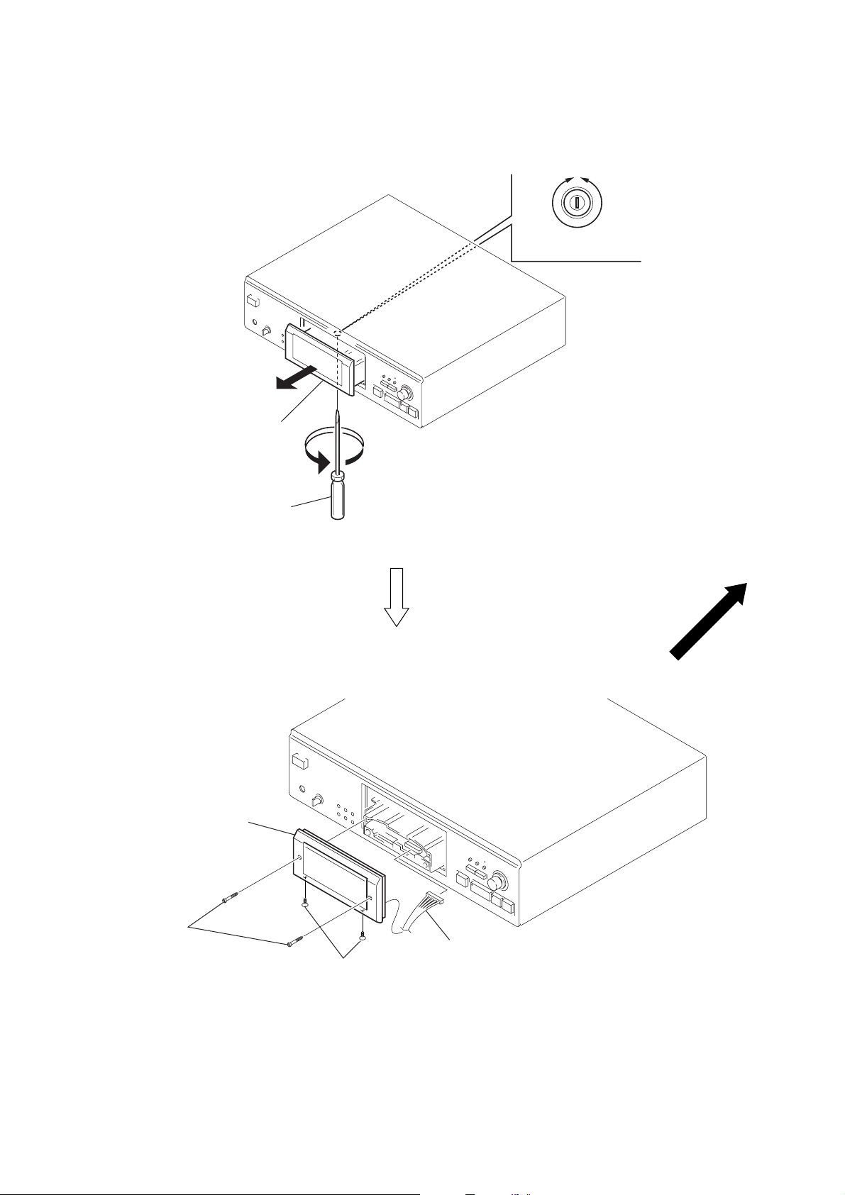
SECTION 3
DISASSEMBLY
Note: Follow the disassembly procedure in the numerical order given.
LOADING PANEL
2
tray
INOUT
– BOTTOM VIEW –
1
Open the tray turning
the tapering screw driver
to the arrow direction.
5
loading panel
3
two hexagon hole
bolt (LID)
4
two screws
(KTP3
×
8)
6
connector (CN292)
8
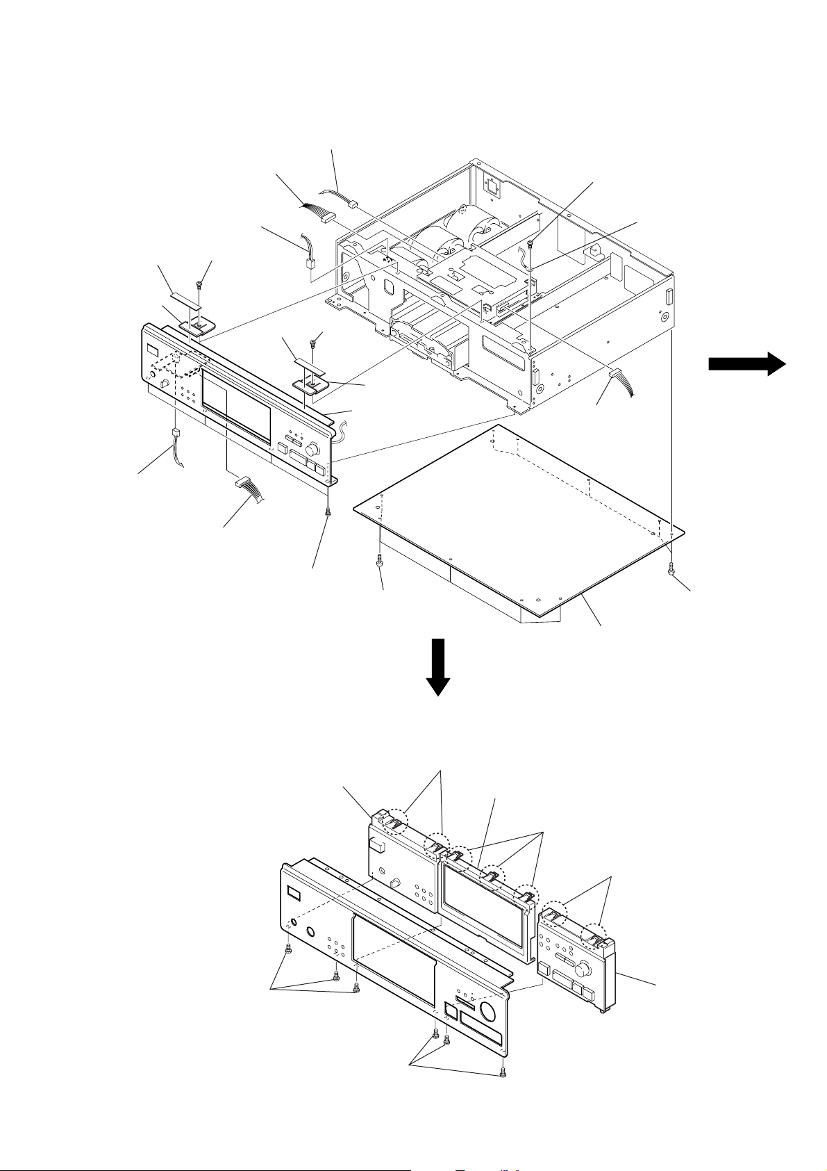
FRONT PANEL
2
bottom plate
1
five screws
(BVTT3
×
8)
1
five screws
(BVTT3
×
8)
qf
four screws
(BVTT3
×
8)
6
screw
(3
×
8)
6
screw
(3
×
8)
5
spacer
3
screw
(BVTT3
×
6)
0
connector
(CN202)
4
harness
8
connector
(CN351)
qa
connector
(CN901)
qs
connector
(CN201)
qd
connector
(CN203)
9
connector
(CN461)
7
bracket
5
spacer
7
bracket
qg
front panel
PANEL (L) , (M) , (R)
1
three screws
(BVTT3
×
8)
7
panel (L)
6
two claws
5
panel (MD)
4
three claws
2
two claws
3
panel (R)
1
three screws
(BVTT3
×
8)
9
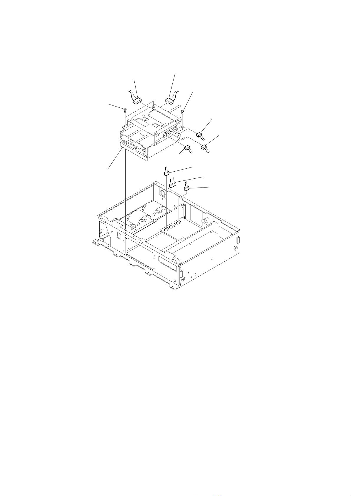
MECHANISM DECK (CDM32BN-12C)
9
two screws
(BVTP3
0
×
6)
mechanism deck
1
connector
(CN251)
5
connector
(CN103)
2
connector (CN91)
9
two screws
(BVTP3
6
connector (CN953)
×
6)
3
connector (CN105)
4
connector (CN104)
7
connector (CN935)
8
connector (CN914)
10
SECTION 4
IC101
TP
(AFJ)
IC204
CN101
y
y
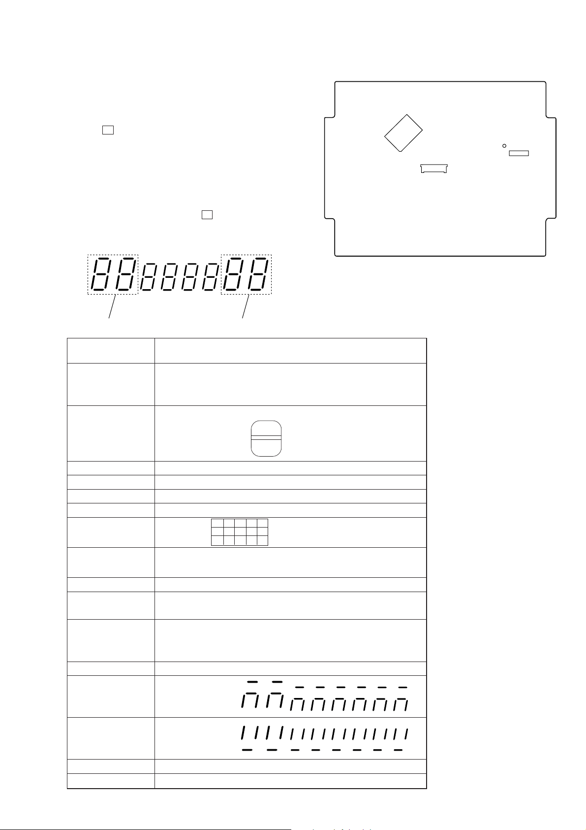
TEST MODE
FLUORESCENT DISPLAY TUBE FULL ON AND
KEY CHECK MODE
Procedure:
1. Connect TP(AFJ) and GND on the SERVO board with a lead
wire.
2. Press ! button to turn the power ON.
3. The fluorescent display tube will fully turn on.
4. Pressing any button causes the set to enter the Key Check mode.
In the Key Check mode, each time a button is pressed, numeric value displayed on the tube is counted up. (However,
once the button is pressed, the value is not counted up even if
pressing the same button again.) Also, while a button is pressed,
its button number is displayed.
5. To exit from the Test mode, press ! button to turn the power
OFF .
7-segment display
Count-up displa
Button Name
PLAY MODE Partial on
Button number displa
Button Number Display
(Display while a button is pressed)
SIDE-A CUSTOM INDEX
FADE
C. SEC
DELETE
– SERVO board (Conductor Side) –
REPEAT Partial on
TIME 000
EDIT/TIME FADE 12
FILE 13
ERASE 00
CHECK Partial on
CLEAR Partial on
FILTER 20
m Partial on
M Partial on
A OPEN/CLOSE Full on
N
Partial on and
nearby LED on
X
Partial on and
nearby LED on
x 888
PUSH ENTER 23
SIDE-B (TIME) (1)
MIN C.FILE
INDEX
135
79
11 13 15
24
6810
12 14 N
1 B (JUST)
PROGRAM
INDEX PEAK
SHUFFLE REPEAT A-
AUTOSPACE EDIT
STEP _
11
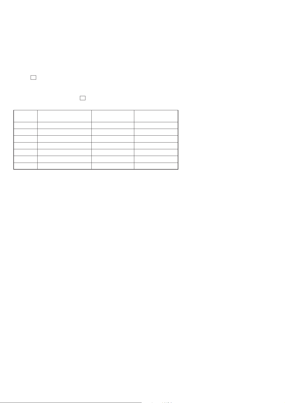
AGING MODE
This set has the Aging mode for operation check of the mechanism deck.
• If a failure occurred
The aging operation stops and a faulty status is displayed on the fluorescent display tube.
• If no failure occurs
The aging operation continues repeatedly.
Note: To enter the Aging mode, the Aging Remote Commander (J-2501-123-A) is required.
1. Press ! button to turn the power ON.
2. Set a disc on the tray.
3. Press [AGING START] button on the Aging Remote Commander.
4. The aging starts, and the fluorescent display tube will display the following.
5. At the completion of aging, press ! button.
Code No. Status
0 Load IN A-0 Err-0
1 Access to TOC A-1 Err-1
2 Access to last track A-2 Err-2
3 Play of last track (3sec) Counter display Err-3
4 Access to first track A-4 Err-4
5 Play of first track (3sec) Counter display Err-5
6 Load OUT A-6 Err-6
Display in Display in
normal operation case of failure
12
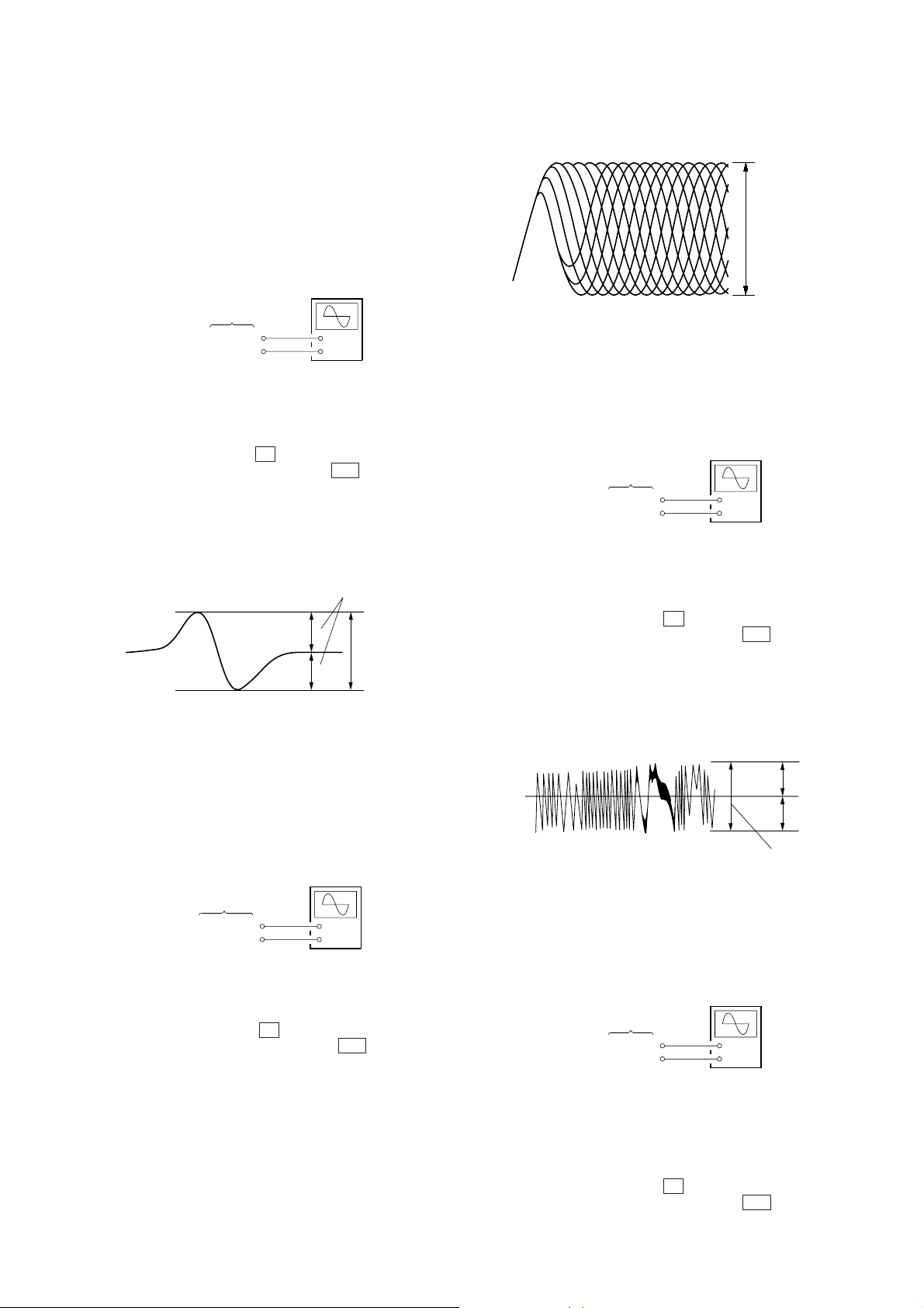
SECTION 5
A
B
level: 1.5 Vp-p
+ 1.5
– 0.5
ELECTRICAL ADJUSTMENTS
Notes:
1. CD block basically constructed to operate without adjustment. Therefore, check each item in order given.
2. Use YEDS-18 disc (Part No.: 3-702-101-01) unless otherwise indicated.
3. Use the oscilloscope with more than 10 MΩ impedance.
4. Clean an object lens by an applicator with neutral detergent when the
signal level is low than specified value with the following checks.
S-Curve Check
Note: Operate with remote commander.
Connection:
oscilloscope
SERVO board
TP (FE)
TP (VC)
+
–
Procedure:
1. Connect the oscilloscope to TP (FE) and TP (VC) on SER VO
board.
2. Connect the TP (ADJ) and GND with lead wire.
3. Turned power switch( ! button) on.
4. Put disc (YEDS-18) in and press the N button. Press the qa
button on remote commander. (actuate the focus search)
5. Confirm that the oscilloscope waveform (S-curve) is symmetri-
cal between A and B. And confirm peak to peak level within
3.0 ± 1.0 Vp-p.
S-curve waveform
symmetry
A
within 3.0
B
±
1.0 Vp-p
RF signal waveform
VOLT/DIV: 200 mV
TIME/DIV: 500 ns
(with the 10 : 1 prove
in use)
level: 1.2 Vp-p
+ 0.25
– 0.20
When observing the eye pattern, set the oscilloscope for AC range
and raise vertical sensitivity.
E-F Balance (Traverse) Check
(Operate with remote commander)
Connection:
oscilloscope
(DC range)
SERVO board
TP (TE)
TP (VC)
+
–
Procedure:
1. Connect the TP (ADJ) to ground with lead wire.
2. Connect the oscilloscope to TP (TE) and TP (VC) on SERVO
board.
3. Turned power switch ( ! button) on.
4. Put disc (YEDS-18) in and press the N button.
5. Press the 3 button on remote commander. (Tracking servo
on)
6. Confirm that the oscilloscope waveform is symmetrical on the
top and bottom in relation to 0 Vdc, and check this level.
6. After check, remove the lead wire connected in step 2.
Note: • Try to measure several times to make sure that the ratio of A : B
or B : A is more than 10 : 7.
• Take sweep time as long as possible and light up the brightness
to obtain best waveform.
RF Level Check
Connection:
oscilloscope
(AC range)
SERVO board
TP (RFO)
TP (VC)
+
–
Procedure:
1. Connect the oscilloscope to TP (RFO) and TP (VC) on SER V O
board.
2. Turned power switch ( ! button) on.
3. Put disc (YEDS-18) in and press the N button.
4. Confirm that the oscilloscope waveform is clear and check RF
signal level is correct or not.
Note: Clear RF signal waveform means that the shape “◊” can be clearly
distinguished at the center of the waveform.
Traverse waveform
7. After check, remove the lead wire connected in step 1.
E-F Balance (Traverse) Check
(No remote commander)
Connection:
oscilloscope
(DC range)
SERVO board
TP (TE)
TP (VC)
+
–
Procedure:
1. Connect the TP (TEI: IC101 pin wj) to TP (VC) with lead
wire.
2. Connect the oscilloscope to TP (TE) and TP (VC) on SERVO
board.
3. Turned power switch ( ! button) on.
4. Put disc (YEDS-18) in and press the N button.
13
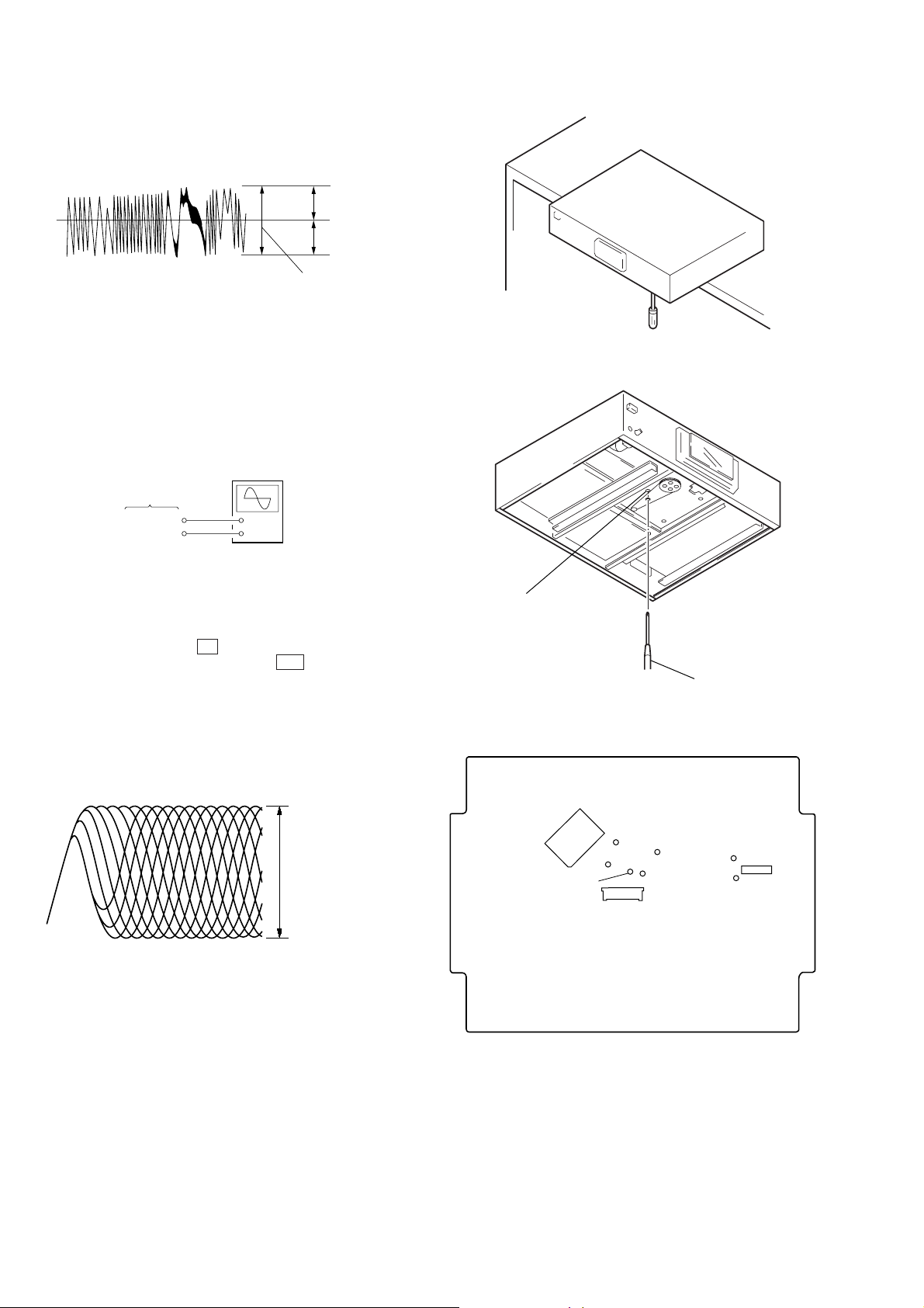
5. Confirm that the oscilloscope waveform is symmetrical on the
e
top and bottom in relation to 0 Vdc, and check this level.
Traverse waveform
A
B
level: 1.5 Vp-p
+ 1.5
– 0.5
6. After check, remove the lead wire connected in step 1.
Skew Adjustment
Note: Do not perform the skew adjustment when not using attached sta-
bilizer to a set.
Connection:
oscilloscop
(AC range)
SERVO board
TP (RFO)
TP (VC)
+
–
Procedure:
1. Remove the bottom plate, put one third of the unit out from
the desk.
2. Connect the osiclloscope to TP (RFO) and TP (VC) on SER V O
board.
3. Turned power switch ( ! button) on.
4. Put disc (YEDS-18) in and press the N button.
5. Adjust to be clear the waveform of the oscilloscope turning
the adjsutment screw with a 3 screwdriver.
Note: Clear RF signal waveform means that the shap “◊”can be clearly
distinguished at the center of the waveform.
6. After the adjustment, lock the adjustment screw.
adjustment screw
– SERVO BOARD (Conductor Side) –
3
screwdriver
RF signal waveform
VOLT/DIV: 200 mV
TIME/DIV: 500 ns
(with the 10 : 1 prove
in use)
level: 1.2 Vp-p
+ 0.25
– 0.20
IC101
TP (FE)
TP (VC)
TP (TEI)
CN101
TP (RFO)
TP (TE)
TP
(AFJ)
IC204
TP
(ADJ)
14
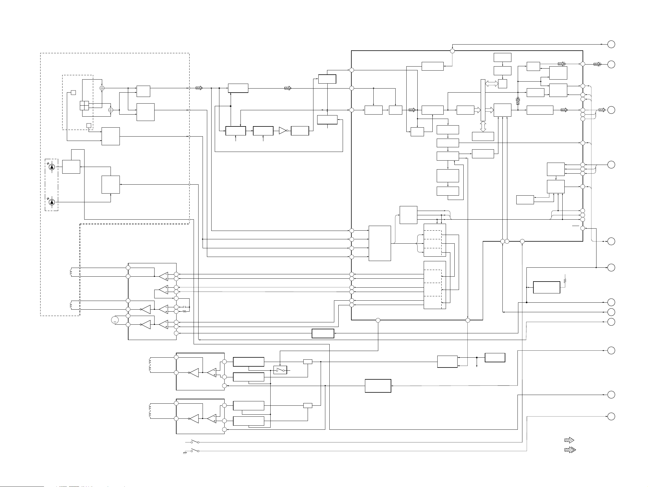
SECTION 6
DIAGRAMS
CDP-XA555ES
6-1. BLOCK DIAGRAM – SERVO Section –
DETECTOR
RF
AMP
FOCUS
ERROR
AMP
FOCUS/TRACKING COIL DRIVE
SLED MOTOR DRIVE
IC102
13
12
27
26
16
17
LD
PD
LASER
DIODE
OPTICAL
PICK-UP BLOCK
(KSS-273B/J1N)
(TRACKING)
2-AXIS
DEVICE
(FOCUS)
LD
DRIVE
E
AC
BD
F
TRACKING
ERROR
AMP
AUTOMATIC
POWER
CONTROL
T+
T–
F+
F–
M21
M
(SLED)
MUTE
10
9
5
4
3
24
23
19
20
15
RFO
LDON
LD VCC
(Page 16)
A
DIGITAL SIGNAL PROCESSOR,
FOCUS/TRACKING/SLED
SERVO, EFM COMPARATOR
IC101
ASYO
39
INTEGRATOR
COMPARATOR
IC106
FE
COMPARATOR
TE
IC107
VC
COMPARATOR
IC108
VC
Q103,104
SWITCHING
Q102
Q101
SWITCHING
Q105, 106
VC
RESET SWITCH
Q151,152
RFAC
36
ASY1
ASYMMETRY
38
CORRECTION
RFDC
26
TE
27
28
29
4
6
8
10
2
100
SE
EF
TRDR
TRDR
FFDR
FRDR
SRDR
SFDR
CONVERTER
LOCK
MUX
M IRR
DFCT
FOK
DETECTOR
A/D
98 96
DIGITAL
PLL
CLOCK
GENERATOR
DEMODULATOR
FOK
DFCT
MIRR
SERVO DSP
FOCUS
SERVO
TRACKING
SERVO
SLED
SERVO
GENERATOR
TRACKING
PWM
GENERATOR
FOCUS
PWM
GENERATOR
SLED
PWM
GENERATOR
EFM
PWM
62
XTAL
SYNC
PROTECTOR
TIMING
GENERATOR 1
CLV SERVO
PROCESSOR
IB TIMS
OVERSAMPLING
FILTER
CLV SERVO
PROCESSOR
REGISTER
MDP
DATA BLIS
ERROR
CORRECTOR
TIMING
GENERATOR 2
PRIORITY
ENCODER
ADDRESS
GENERATOR
32K
RAM
D/A
DATA
PROCESSOR
GFS
MUTE
79 54 99
SERVO
INTERFACE
S STOP
DIGITAL
OUT
PEAK
DETECTOR
SERIAL/PARALLEL
PROCESSOR
SIGNAL
GENERATOR RESET
IC204
SUBCODE
P-W
PROCESSOR
SUBCODE
Q
PROCESSOR
CPU
INTERFACE
SERVO
AUTO
SEQUENCER
+5V
DOUT
SUBQ
SQCK
SCLK
DATA
LRCK
BCLK
SCOR
DATA
XLAT
CLK
SENS
FOK
DFCT
MIRR
XRST
71
77
78
83
46
45
47
74
86
87
88
80
93
92
91
81
B
C
D
E
F
G
H
I
(Page 16)
(Page 16)
(Page 16)
(Page 16)
(Page 16)
(Page 16)
(Page 16)
(Page 16)
L11–13
BSL
(SPINDLE)
L11
L12
L14
L13
SPINDLE MOTOR DRIVE
1
2
SPINDLE MOTOR DRIVE
1
2
+5V
IC104
IC105
(LIMIT IN)
(LIMIT OUT)
S22
S21
MUTE
MUTE
5
4
15
5
4
15
CONSTANT CURRENT
Q172
CONSTANT CURRENT
Q171
CONSTANT CURRENT
Q182
CONSTANT CURRENT
Q181
Q190
D+5V
H11
H12
(Page 16)
J
K
L
(Page 16)
(Page 16)
VC
COMPARATOR
IC110, 111
H
MUTING CONTROL
SWITCH
Q153,154
H
SPINDLE
MOTOR DRIVE
IC103
• SIGNAL PATH
: CD PLAY
: DIGITAL OUT
R-CH : Same as L-CH
1515
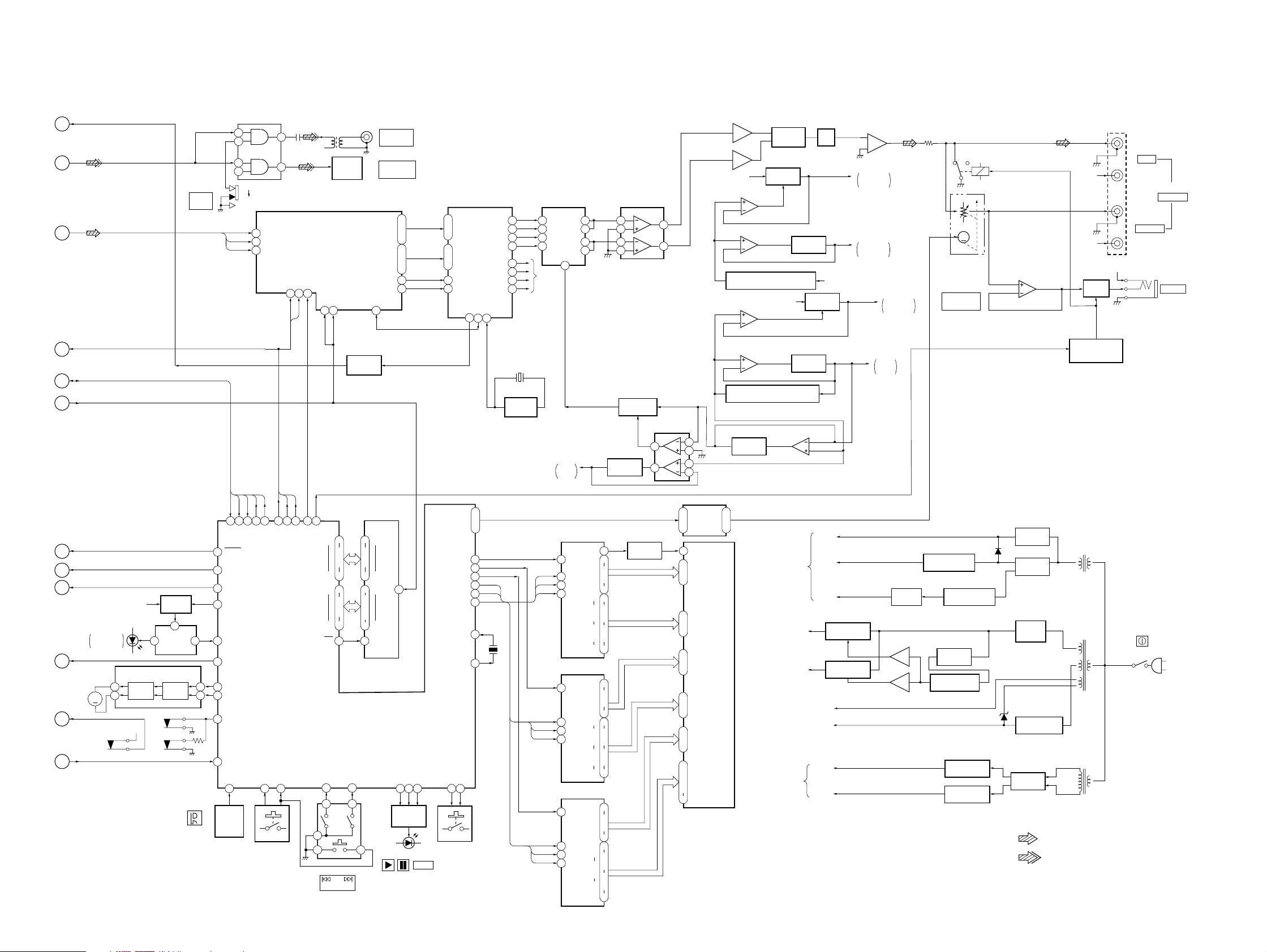
CDP-XA555ES
6-2. BLOCK DIAGRAM – MAIN Section –
(Page 15)
(Page 15)
(Page 15)
(Page 15)
(Page 15)
(Page 15)
A
B
C
DATA, XLAT, CLK
D
SCLK, SQCK, SUBQ, SCOR, SENSE
E
F
S705
DIGITAL
OUT
WAVE SHAPER
IC702
2
1
5
6
OFF
ON
DATA
48
LRCK
50
BCLK
49
DATA
LRCK I
BCKI
7
3
SC DATA
SHIFT
33 32 31
CLK
DATA
T710
OPTICAL
DIGITAL FILTER
IC600
LATCH
INIT
NREGCLR
28 30
OUT
IC701
CLOCK OSC
IC109
DIGITAL OUT
COAXIAL
JC701
OPTICAL OUT
OPTICAL
NSDOL1
|
NSDOL4
NSDOR1
|
NSDOR4
XIN
DINT
64FSI
10
J710
Q404
IC403 (1/2)
REGULATOR
1
REG AMP
IC604 (2/2)
7
Q604
7
IC605 (2/2)
1
Q605
MIX AMP
Q607
+20V
7
REGULATOR AMP
Q403
–20V
REG AMP
IC604 (1/2)
3
2
5
6
REFERENCE VOLTAGE GENERATOR
REGULATOR AMP
IC605 (1/2)
5
6
REGULATOR AMP
3
2
REFERRENCE VOLTAGE GENERATOR
6
5
3
2
REGULATOR
Q601
79
76
2
5
26
29
23
20
X600
45MHz
IC607
CURRENT PULSE
D/A CONVERTER
IC401
25
IN1+
24
IN1–
27
IN2+
28
IN2–
16
R-CH
IC501
B+
IC607
IC601
IO1+
IO2–
IO1–
IO2+
C5
I-V CONVERSION
IC402
1
2
4
5
6
5
2
3
REG CONT SW
Q401,402
REGULATOR
Q600
7
1
REGULATOR AMP
IC603
7
1
D/A CONVERTER
IC601
1
•
3
•
6
•
8
17
•
19
•
22
•
24
13
40
56
NSDTIL1
|
59
NSDTIL4
46
NSDTIR1
|
49
NSDTIR4
F512FSO R2(+)
51
MUTE
39
|
|
LVCK01
69
54
NSBCK013XIN
L1(+)
L1(–)
L2(+)
L2(–)
R1(+)
R1(–)
R2(–)
CLOCK OSC
REGULATOR
Q602
REGULATOR
REGULATOR
Q603
6
5
IC602
LPF
–15V
Q606
AUDIO AMP
IC403(2/2)
2
+
3
–
B–
IC502, 503,
IC402, 403
B–
IC501, 602,
IC401, 603
IC501,
IC401
1
B+
IC502, 503,
IC402, 403
B+
M
RV352
LINE OUT
PHONE LEVEL
RY491
IC606
HEADPHONE AMP
5
6
7
R-CH
R-CH
MUTING
Q451
MUTE
CONTROL SWITCH
Q608, 609
R-CH
L
FIXED
R
L
VARIABLE
R
PJ471
LINE OUT
J461
PHONES
(Page 15)
(Page 15)
(Page 15)
(Page 15)
(Page 15)
(Page 15)
G
H
I
J
M271
(LOADING)
K
L
STABILIZER
DETECT
M
S283
(LD)
+5V
D202
LOADING MOTOR DRIVE
2
MOTOR
DRIVE
10
+5V
IC205
S281
(IN)
S282
(OUT)
B+ SWITCH
Q201,202
1
STABILIZER
DETECT
IC203
CONTROL
LOGIC
49 60 52 51 46 50 63 48 47 61
SCOR
SENSE
RESET
30
DMUTE
67
LDON
62
SENSOR SW
27
SENSOR
24
28
SPDL-MUTE
17
LOAD IN
5
65
LOAD OUT
6
64
IN/OUT SW
45
LIMIT OUT
29
RMIN
56
REMOTE
CONTROL
RECEIVER
IC804
SUBQ
SCLK
SQCK
K2
S884–892
41K340
DATA
XLT
CLK
PRGL
68
D0
AMUTE
71
•
74
77
D7
78
A0
80
•
1
10
A12
WE
11
K4
42 42
3 5
4
1 2
RV870
AMS
PUSH ENTER
S-RAM
IC202
15
D0
19
•
13
11
D7
10
A0
2
•
21
•
23
25
A12
WE
27
SYSTEM CONTROL
K5
26
CE2
IC201
LED PLAY
LED PAUSE16LED PD/00N
14
15
LED
DRIVE
Q871–873
D871, 872, S886 (2/2)
FILTER
VOL UP
VOL DOWN
CLK
BLK
38K039
S850–855
VOLUME
19
•
20
22
D0
23
D1
24
D2
CLK
25
WR
26
WR
BLK
21
31
32
X201
4MHz
K1
CLK
WR
BLK
CLK
WR
BLK
CLK
BLK
FL DRIVER
IC803
S1
DATA
46
S2
|
CL
45
44
2
46
45
44
2
46
45
44
2
WR
BLK
FL DRIVER
IC802
DATA
CL
WR
BLK
FL DRIVER
IC801
DATA
CL
WR
BLK
S13
S14
S26
S27
S41
6A
6G
•
7A
7G
•
8A
8G
|
3A
3G
•
4A
4G
•
5A
5G
|
1A
1G
•
2A
2G
WR
SWITCHING
18 66
Q801,802
17
14
•
12
5
42
39
•
37
25
•
23
20
18
14
•
12
5
42
39
•
37
25
•
23
20
18
14
•
12
5
35
37
•
39
42
•
34
28
3
MOTOR
•
DRIVER
2
IC350
S1
S2
67
|
|
S13
78
FLD801
FLUORESCENT
INDICATOR TUBE
6A–6G,
34
7A–7G,
|
8A–8G
54
S14
79
|
|
S26
91
13
3A–3G,
|
4A–4G,
33
5A–5G
S27
92
|
|
S41
106
113
|
1A–1G,
107
2A–2G
•
6
12
7
•
8
DVd+5V
SYSTEM CONTROLLER(IC201)
D/A CONVERTER(IC601)
AUDIO
SECTION
DVa+5V
SERVO B+
SERVO
SECTION
R+10V
+15V
–15V
+5V REGULATOR
+5V REGULATOR
FLD801 F
–18V
FL DRIVER B–
(IC801, 802, 803)
SV+7V
SV–7V
Q932
Q930
RECTFIER
D911
IC630(1/2)
IC630(2/2)
+15V REGURATOR
IC910
–15V REGURATOR
IC911
REGULATOR
IC931
REGULATOR CONT
Q931,D931
+7V REGULATOR
IC950
–7V REGULATOR
IC951
D930
D915
–18V REGULATOR
D957,958
• SIGNAL PATH
RECTFIER
D920
RECT
D916–919
RECT
D935,936
D939,940
IC932
RECT
T901
POWER
TRANSFORMER
(FOR ANALOG)
T902
POWER
TRANSFORMER
(FOR DIGITAL)
T903
POWER
TRANSFORMER
(FOR DRIVE)
: CD PLAY
: DIGITAL OUT
R-CH : Same as L-CH
S991
(POWER)
AC IN
1616
D
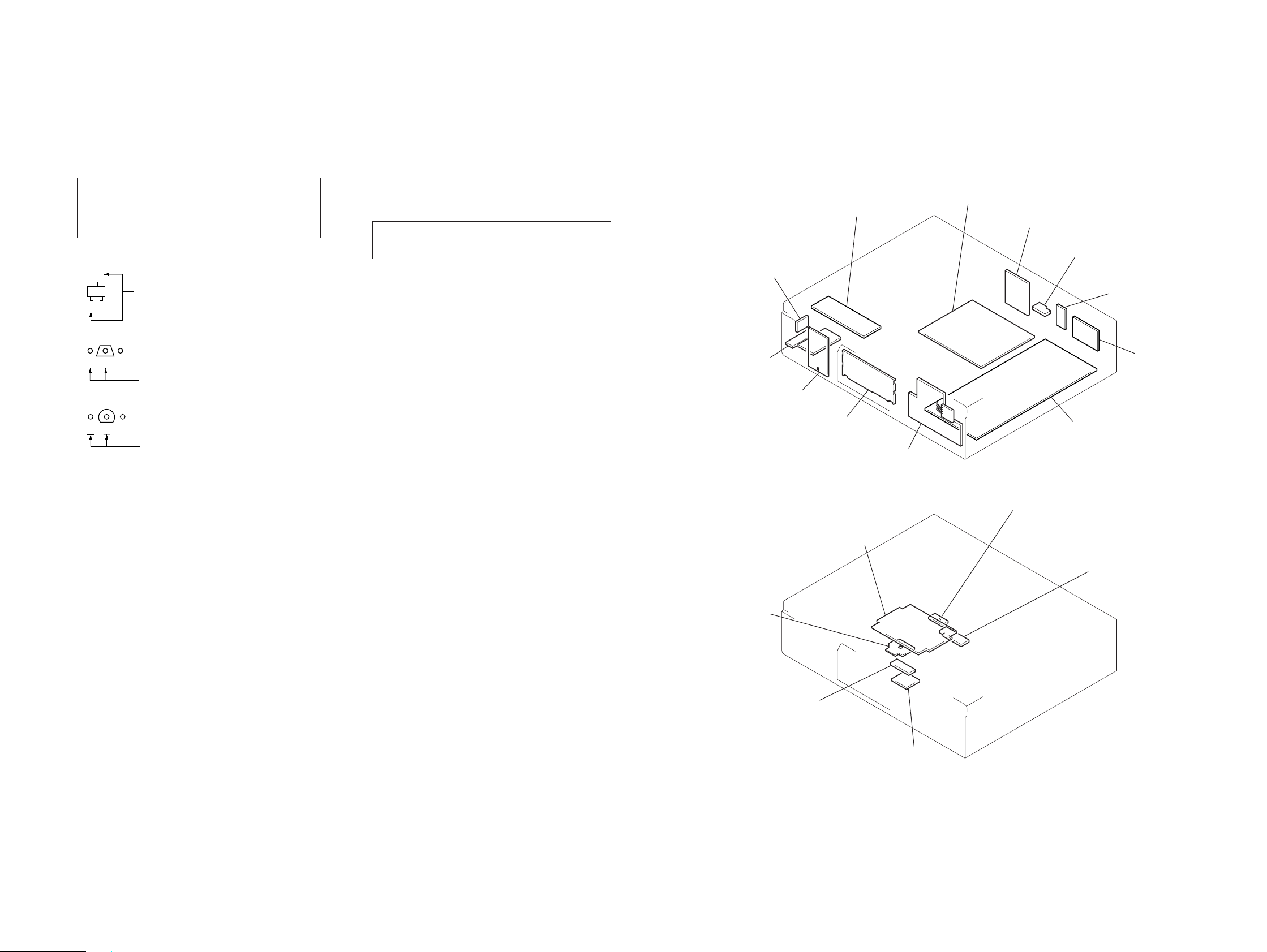
6-3. NOTES FOR PRINTED WIRING BOARD AND SCHEMATIC DIAGRAM
• Circuit Boards Location
Note on Printed Wiring Board:
• X : parts extracted from the component side.
• Y : parts extracted from the conductor side.
®
•
• b : Pattern from the side which enables seeing.
(The other layers' patterns are not indicated.)
Caution:
Pattern face side: Parts on the pattern face side seen from
(Conductor Side) the pattern face are indicated.
Parts face side: Parts on the parts face side seen from
(Component Side) the parts face are indicated.
• Indication of transistor.
: Through hole.
C
Q
B
E
These are omitted.
Q
B
CE
These are omitted.
Q
B
CE
These are omitted.
Note on Schematic Diagram:
• All capacitors are in µF unless otherwise noted. pF: µµF
50 WV or less are not indicated except for electrolytics
and tantalums.
• All resistors are in Ω and 1/
specified.
• % : indicates tolerance.
¢
•
• 5 : fusible resistor.
• C : panel designation.
Note: The components identified by mark ! or dotted line
• U : B+ Line.
• V : B– Line.
• H : adjustment for repair.
• Voltages and wa vef orms are dc with respect to ground in
• Voltages are taken with a V OM (Input impedance 10 MΩ).
• Waveforms are taken with a oscilloscope.
• Circled numbers refer to waveforms.
• Signal path.
: internal component.
with mark ! are critical for safety.
Replace only with part number specified.
CD play mode.
no mark : CD PLAY
Voltage variations may be noted due to normal production tolerances.
Voltage variations may be noted due to normal production tolerances.
J : CD PLAY
c : digital out
4
W or less unless otherwise
SW BOARD
VR BOARD
KEY-L BOARD
AC BOARD
DISPLAY BOARD
POWER BOARD
COAX OUT BOARD
OPT OUT BOARD
D/O SW BOARD
LINE OUT BOAR
AUDIO BOARD
KEY-R BOARD
LOADING MOTOR BOARD
SERVO BOARD
FLEX RELAY BOARD
BSL BOARD
FL BOARD
LOADING SW BOARD
1717
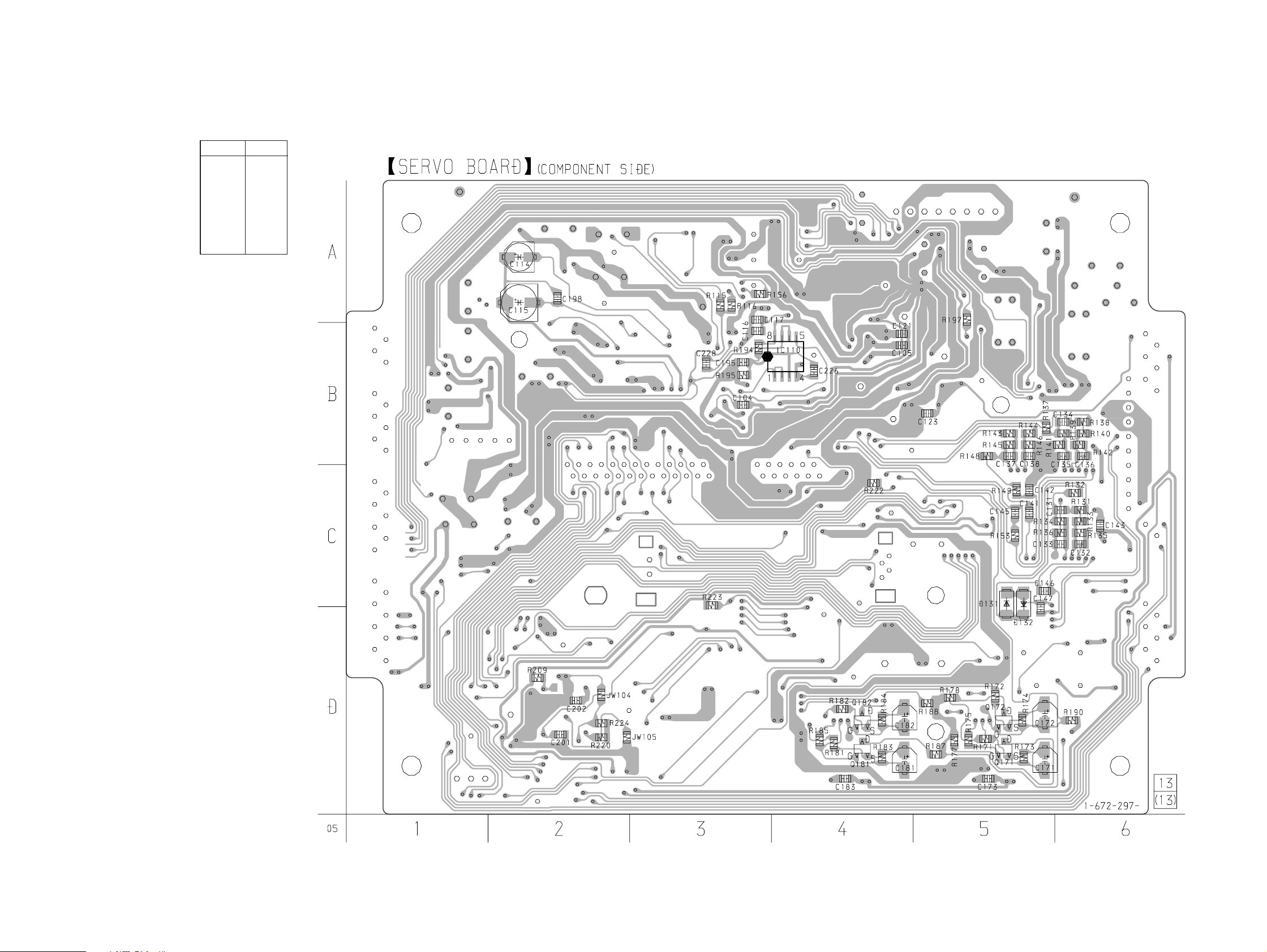
CDP-XA555ES
6-4. PRINTED WIRING BOARD – SERVO Board (Component Side) – • See page 17 for Circuit Boards Location.
• Semiconductor
Location
Ref. No. Location
D131 C-5
D132 C-5
IC110 B-4
Q171 D-5
Q172 D-5
Q181 D-4
Q182 D-4
1818
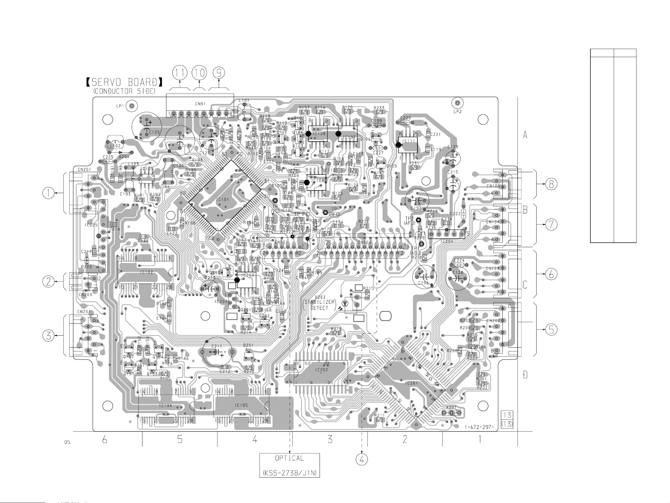
CDP-XA555ES
6-5. PRINTED WIRING BOARD – SERVO Board (Conductor Side) – • See page 17 for Circuit Boards Location.
(Page 35) (Page 25)
(Page 22)
(Page 35)
(Page 28)
(Page 25)
• Semiconductor Location
Ref. No. Location
D201 D-4
D202 C-3
D203 C-6
D204 A-6
IC101 B-5
IC102 C-5
IC103 C-4
IC104 D-5
IC105 D-4
IC106 B-3
IC107 A-3
IC108 A-3
IC109 B-5
IC111 A-2
IC201 D-2
IC202 D-3
IC203 C-4
IC204 B-2
IC205 B-6
Q101 A-4
Q102 A-3
Q103 A-3
Q104 A-3
Q105 A-2
Q106 A-2
Q151 D-6
Q152 D-6
Q153 D-5
Q154 D-5
Q190 C-5
Q201 C-4
Q202 C-4
(Page 30)
(Page 30)
(Page 25)
(Page 30)
PICK UP BLOCK
(Page 22)
1919
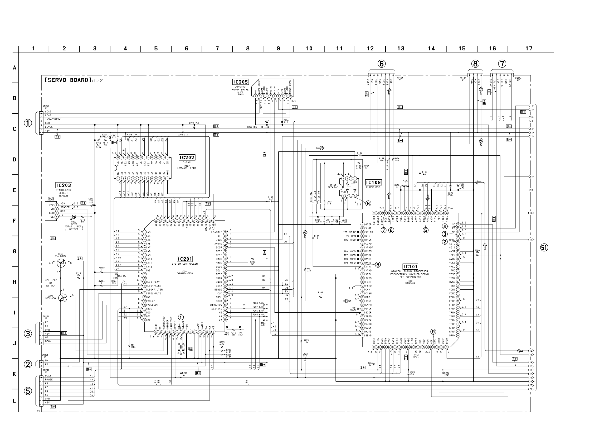
CDP-XA555ES
6-6. SCHEMATIC DIAGRAM – SERVO Board (1/2) – • See page 37 for Waveforms. • See page 38 for IC Block Diagrams.
(Page 23)
(Page 26)
(Page 29)
(Page 26)
(Page 31)
(Page 31)
(Page 31)
(Page 21)
2020
 Loading...