

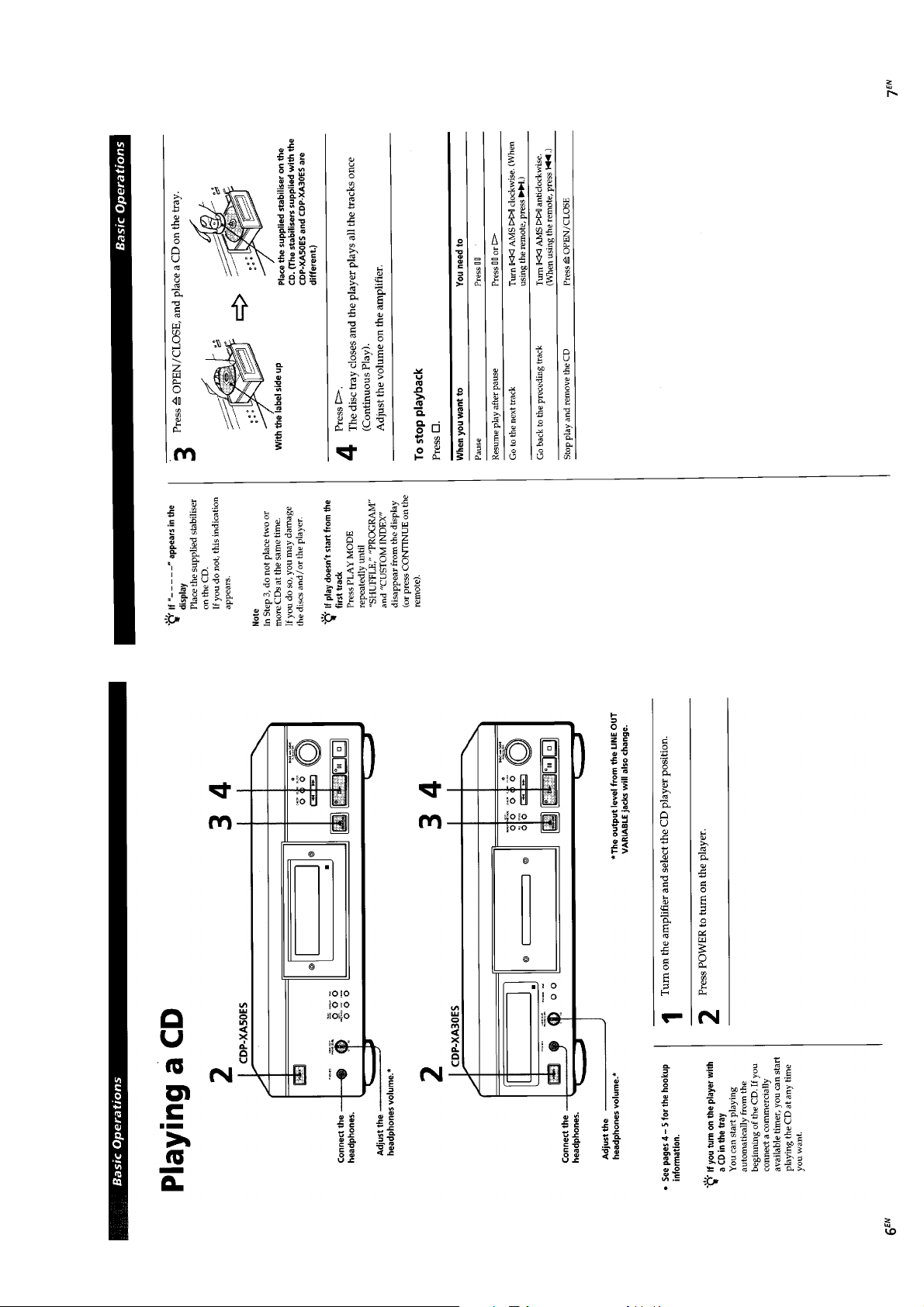
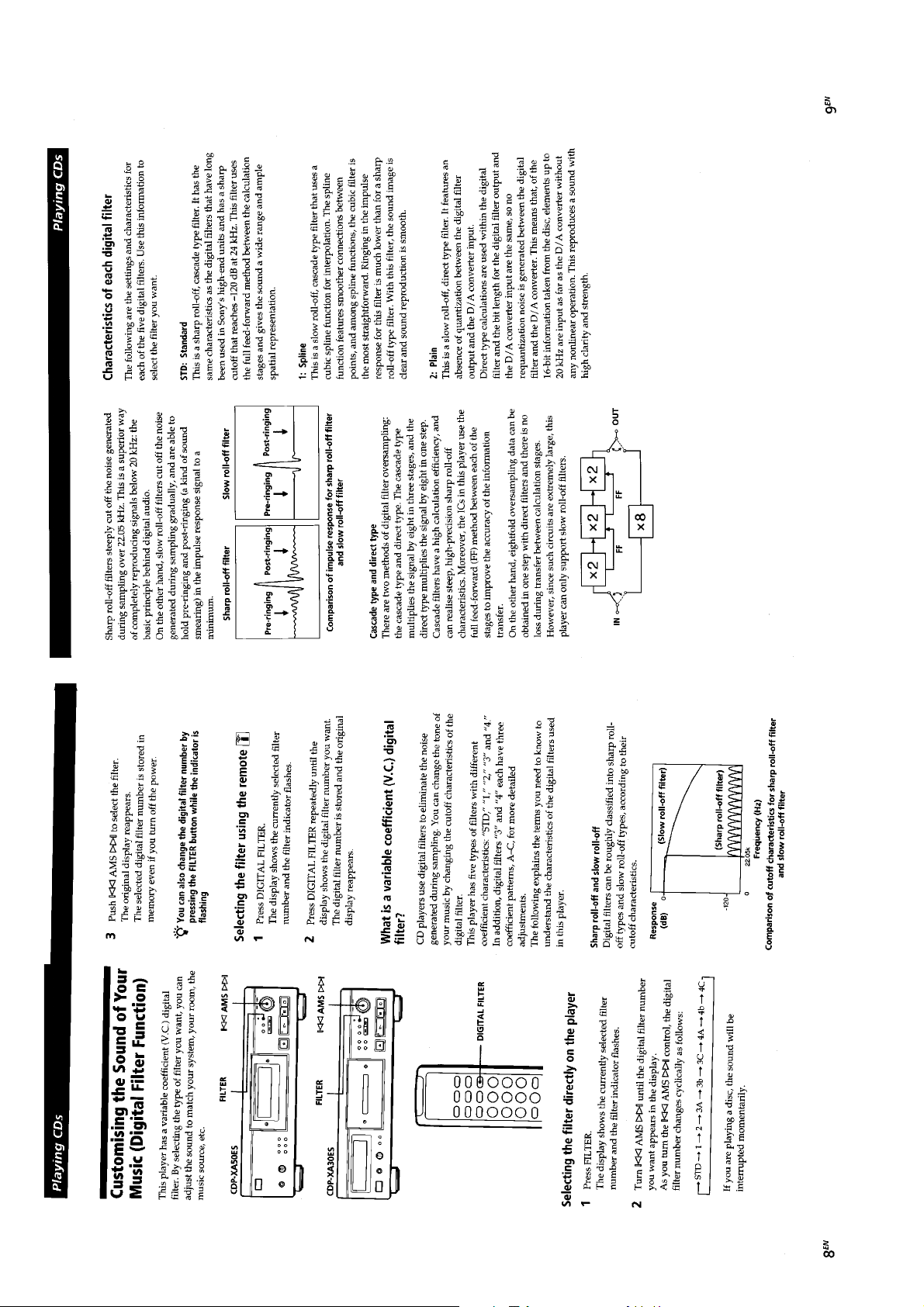
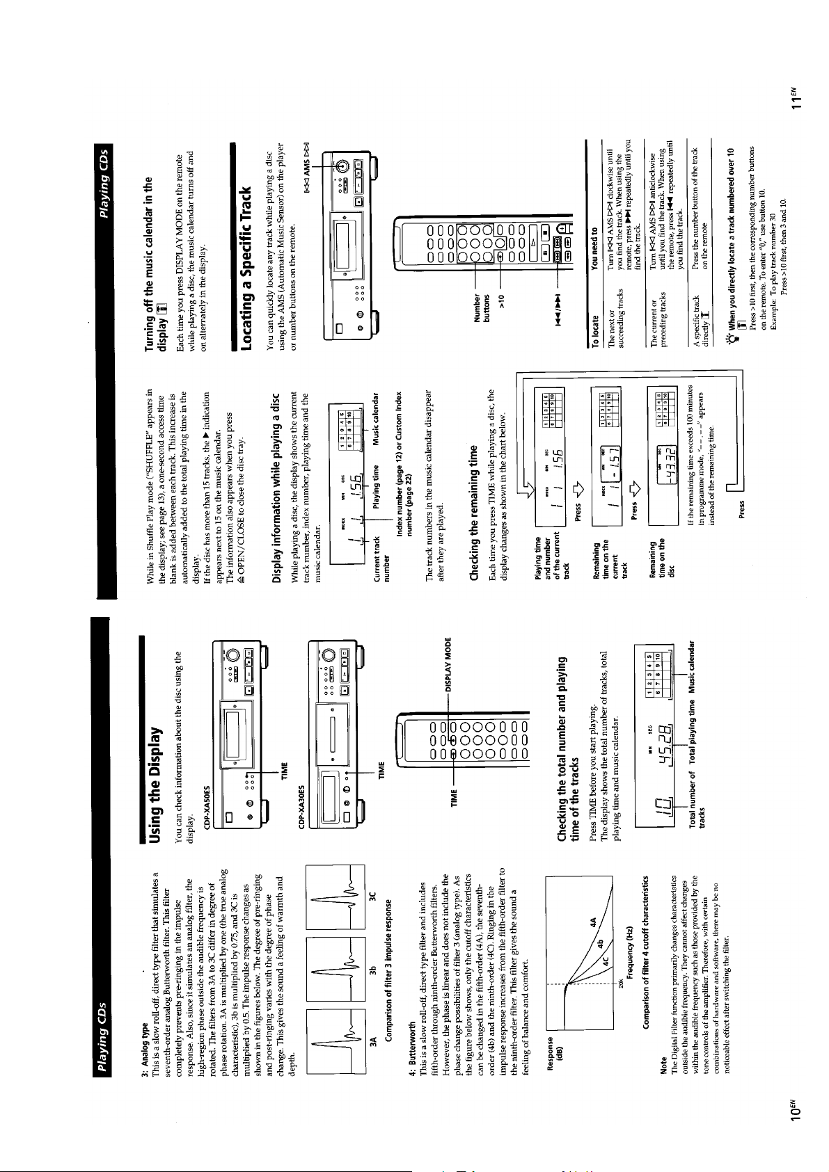
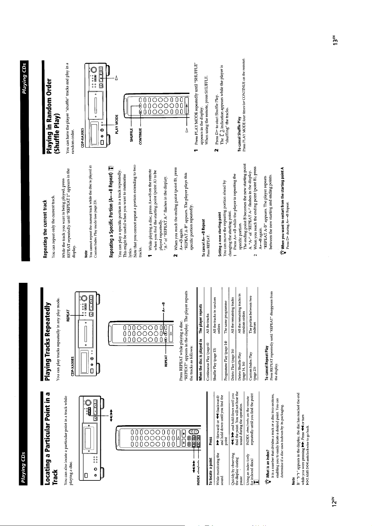
CDP-XA30ES
SERVICE MANUAL
Photo : Gold
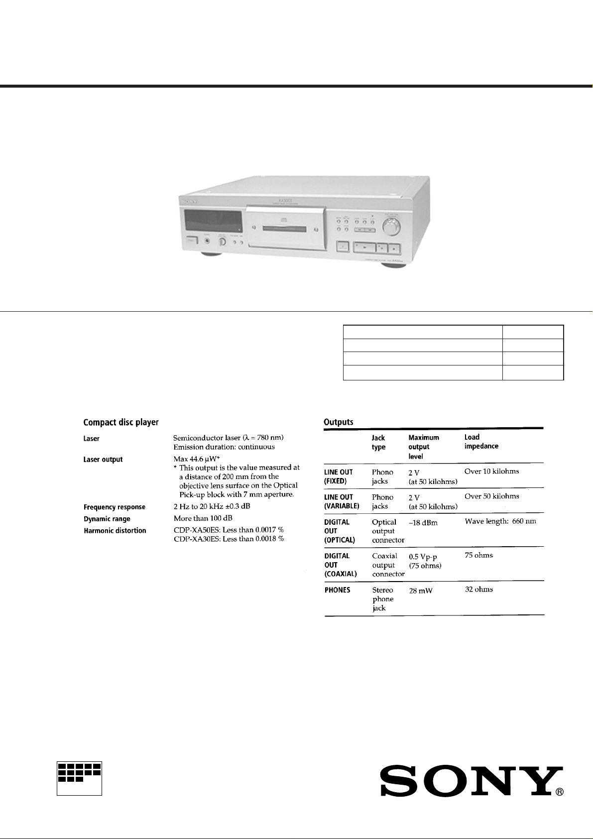
SPECIFICATIONS
AEP Model
E Model
Model Name Using Similar Mechanism NEW
CD Mechanism Type
Base Unit Type BU-14A
Optical Pick-up Type KSS-213B
CDM36A-14A
MICROFILM
– Continued on next page –
COMPACT DISC PLAYER
MODEL IDENTIFICATION
– BACK PANEL –
TABLE OF CONTENTS
1. SERVICING NOTES
1-1. How to Open the Disc Tray When Power Switch
Turns Off.......................................................................... 3
1-2. Preparation for Adjustment and Measurement ................ 3
2. GENERAL ................................................................... 4
3. DISASSEMBLY.......................................................... 15
4. TEST MODE
4-1. AF Mode.......................................................................... 19
4-2. ADJ Mode ....................................................................... 20
5. ELECTRICAL ADJUSTMENTS .......................... 21
6. DIAGRAMS
6-1. IC PIN FUNCTION DISCRIPTION............................... 23
6-2. Block Diagram................................................................. 35
6-3. Printed Wiring Boards –BD Section –............................. 38
6-4. Schematic Diagram — BD Section — ............................ 41
6-5. Schematic Diagram — MAIN Section — ....................... 46
6-6. Printed Wiring Boards — MAIN Section —................... 51
6-7. Schematic Diagram — PANEL Section — ..................... 55
6-8. Printed Wiring Boards — PANEL Section —................. 59
7. EXPLODED VIEWS ................................................. 61
4-986-682-
AEP MODEL : 1 π (CED)
Singapore Model : 2
π
(SP)
8. ELECTRICAL PARTS LIST .................................. 66
SAFETY-RELATED COMPONENT WARNING!!
COMPONENTS IDENTIFIED BY MARK ! OR DOTTED
LINE WITH MARK ! ON THE SCHEMATIC DIAGRAMS
AND IN THE PARTS LIST ARE CRITICAL TO SAFE
OPERATION. REPLACE THESE COMPONENTS WITH
SONY PARTS WHOSE PART NUMBERS APPEAR AS
SHOWN IN THIS MANUAL OR IN SUPPLEMENTS PUBLISHED BY SONY.
– 2 –
SECTION 1
SERVICING NOTES
NOTES ON HANDLING THE OPTICAL PICK-UP
BLOCK OR BASE UNIT
The laser diode in the optical pick-up block may suffer electrostatic break-down because of the potential difference generated
by the charged electrostatic load, etc. on clothing and the human
body.
During repair, pay attention to electrostatic break-down and also
use the procedure in the printed matter which is included in the
repair parts.
The flexible board is easily damaged and should be handled with
care.
NOTES ON LASER DIODE EMISSION CHECK
The laser beam on this model is concentrated so as to be focused
on the disc reflective surface by the objective lens in the optical
pick-up block. Therefore, when checking the laser diode emission, observe from more than 30 cm away from the objecti ve lens.
Notes on chip component replacement
• Never reuse a disconnected chip component.
• Notice that the minus side of a tantalum capacitor may be dam-
aged by heat.
Flexible Circuit Board Repairing
• Keep the temperature of the soldering iron around 270 ˚C dur-
ing repairing.
• Do not touch the soldering iron on the same conductor of the
circuit board (within 3 times).
• Be careful not to apply force on the conductor when soldering
or unsoldering.
CAUTION
Use of controls or adjustments or performance of
procedures other than those specified herein may
result in hazardous radiation exposure.
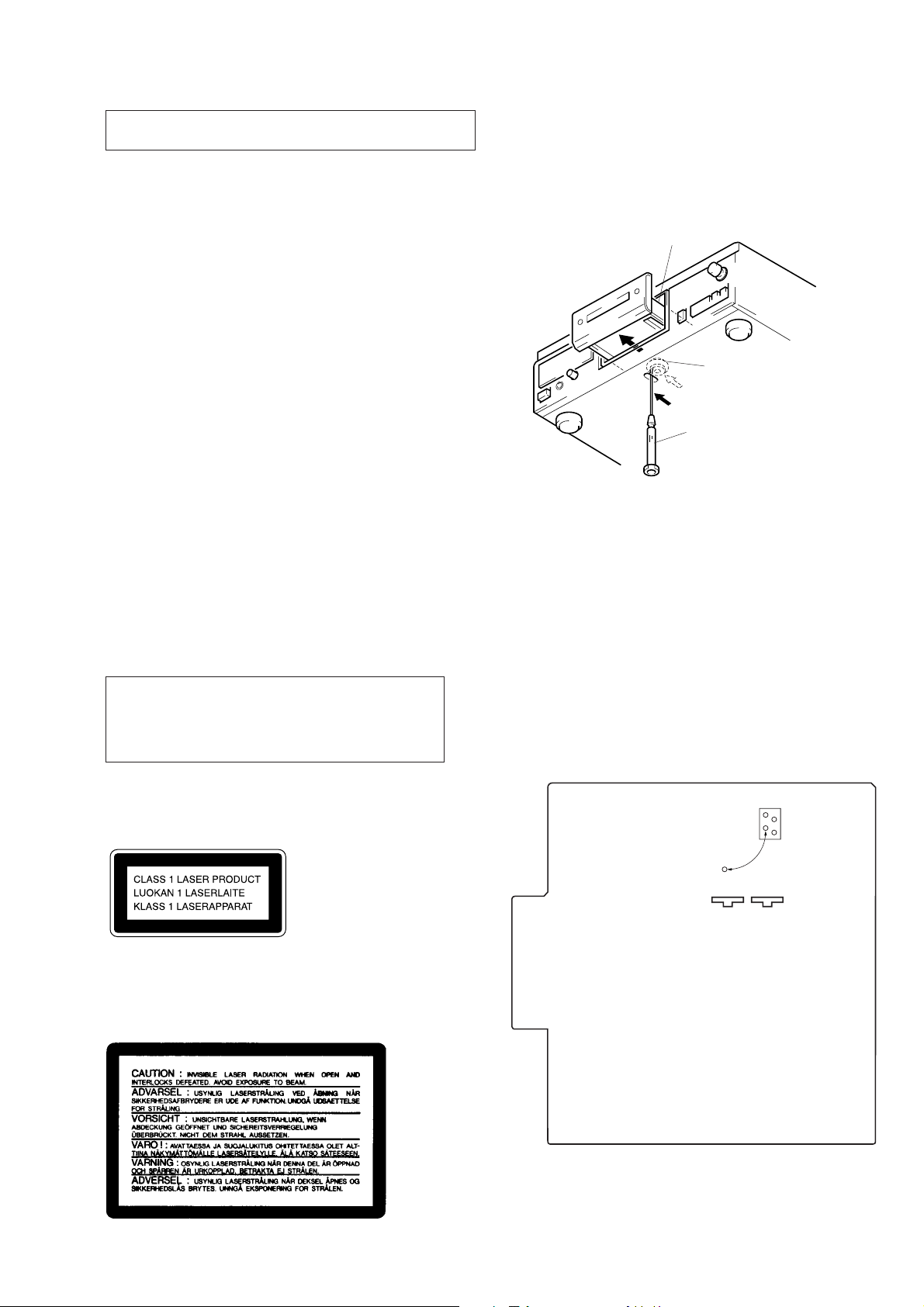
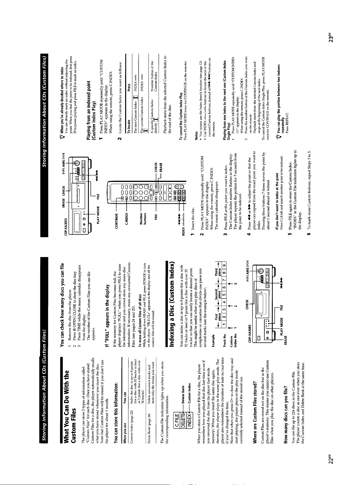
1-1. H OW T O OPEN THE DISC TRAY WHEN
POWER SWITCH TURNS OFF
1 Insert a tapering driver into the aperture of the unit bottom,
and move the limiter (LEVER) to direction of the arrow A.
2 Pull the tray to direction fo the arrow B.
tray
B
Limiter (LEVER)
A
tapering driber
*
To close the disc tray, move the driver in
the reverse direction (to IN direction).
1-2. PREPARATION FOR ADJUSTMENT AND
MEASUREMENT
Perform connecting the IC361 pin 2 of BD board to the line of
+5V because this unit does not work without the stabilizer structurally.
Connecting Location:
[BD BOARD] (SIDE B)
This appliance is classified as a CLASS 1 LASER product.
The CLASS 1 LASER PRODUCT MARKING is located on
the rear exterior.
Laser component in this product is capable of emitting radiation
exceeding the limit for Class 1.
The following caution label is located inside the unit.
Q301
+5V
IC361
2
1
Q302
– 3 –
SECTION 2
GENERAL
This section is extracted
from instruction manual.
– 4 –
– 5 –
– 6 –
– 7 –
– 8 –
– 9 –
– 10 –
– 11 –
– 12 –
– 13 –
– 14 –
• This set can be disassembled in the order shown below.
SECTION 3
DISASSEMBLY
LOADING PANEL
SECTION
(Page 15)
Note: Follow the disassembly procedure in the numerical order given.
CASE,
FRONT PANEL SECTION
(Page 16)
LOADING PANEL SECTION
MECHANISM
DECK SECTION
(Page 16)
BASE UNIT
(Page 17)
LOADING MOTOR
(Page 18)
POWER BOARD, MAIN BOARD
(Page 18)
OPTICAL PICK-UP
(Page 17)
4
loading panel section
3
two hexagon hole bolts
(LID)
B
2
Pull the loading panel to
direction of the arrow
A
1
B
.
limiter (LEVER)
Insert a tapering driver,
and move the limiter (LEVER)
to direction of the arrow
A
.
– 15 –
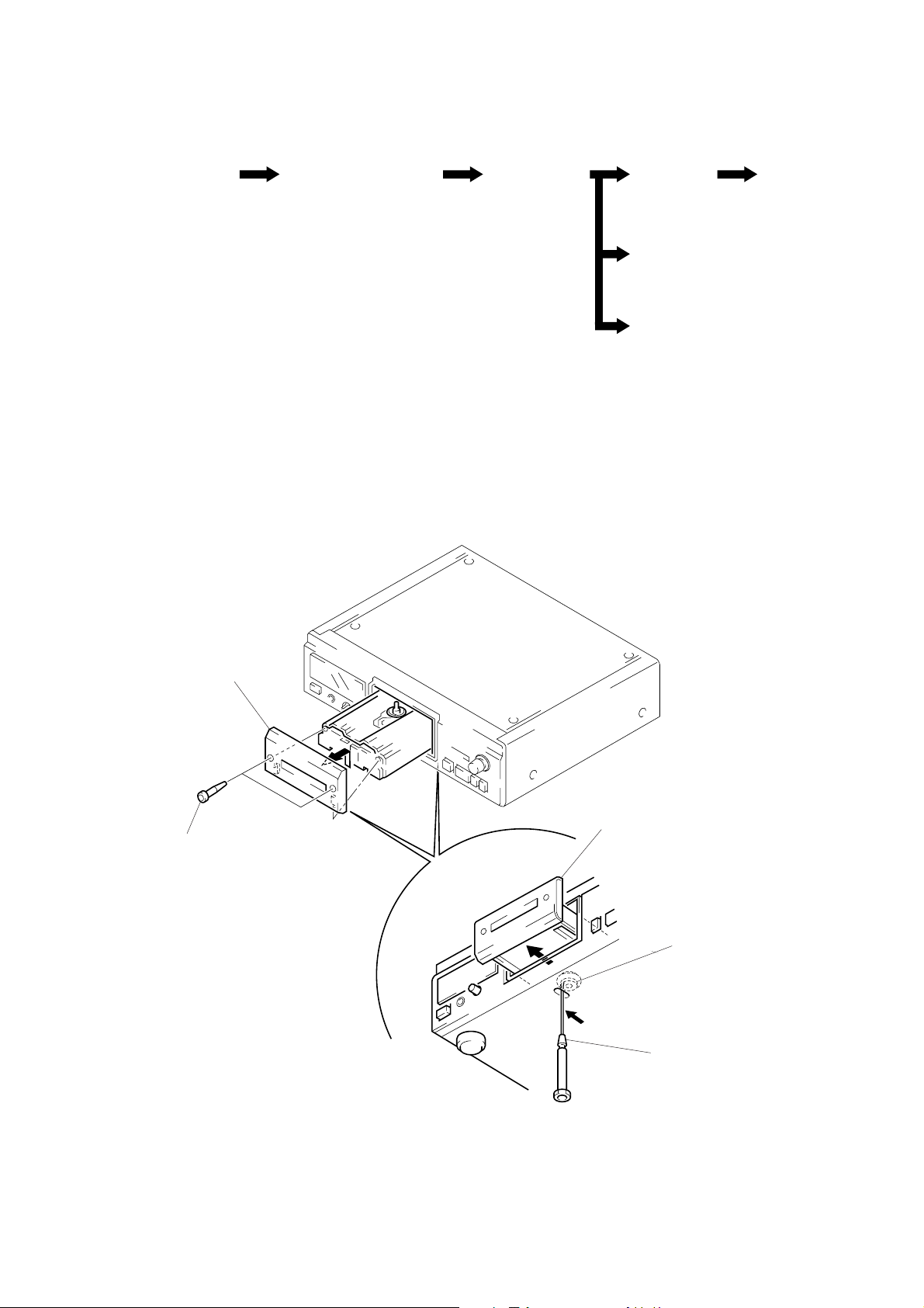
CASE, FRONT PANEL SECTION
7
connector
(CN407)
1
four screws
(CASE 3 TP2)
9
connector
(CN992)
3
case
2
screw
(BVTT3
×
6)
1
four screws
(CASE 3 TP2)
!∞
front panel
HP board
8
connector
(CN402)
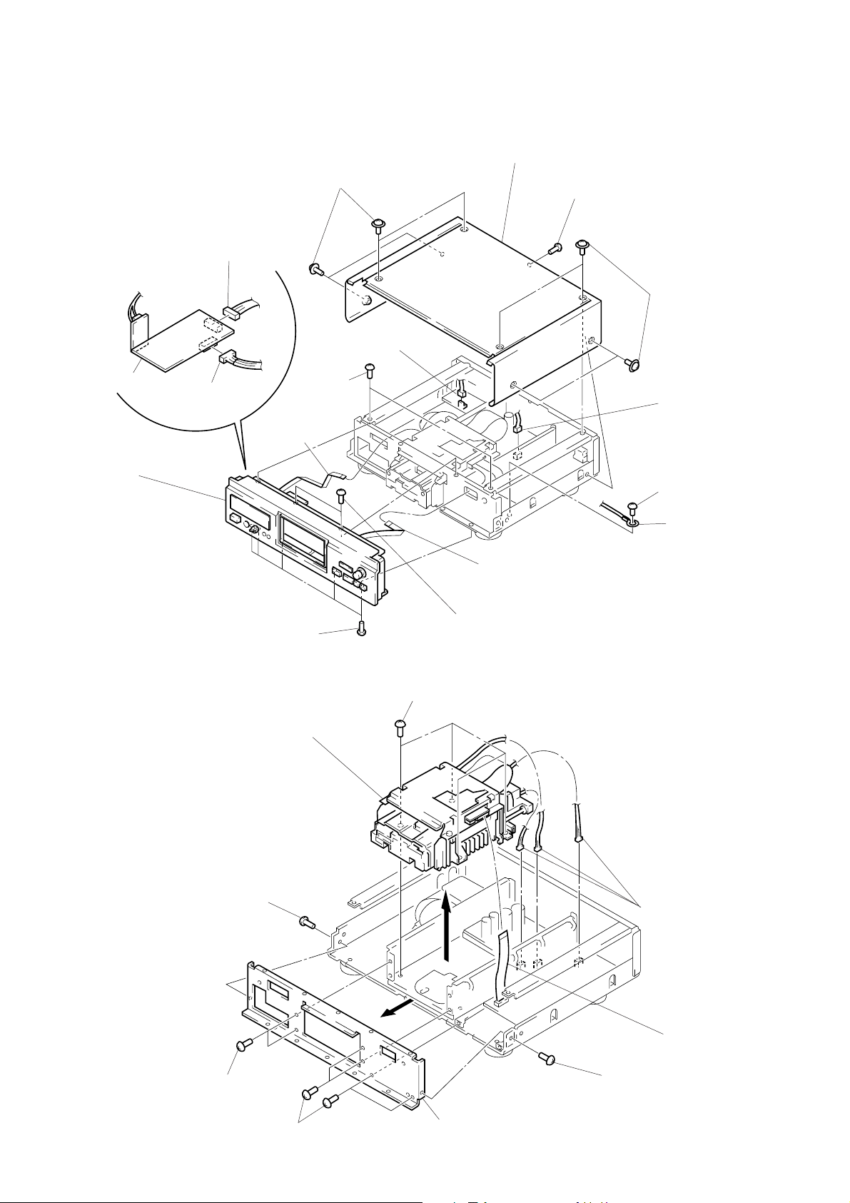
MECHANISM DECK SECTION
0
5
flat wire (10 core)
(CN106)
!£
five screws
(BV3
×
8)
6
mechanism deck
(CDM36A-14A)
two screws
(BVTT3
×
6)
5
four screws
(BVTT3
!¢
×
6)
6
flat wire (9 core)
(CN107)
two screws
(BVTT3
×
6)
4
connector
(CN206)
!¡
screw
(BVTT3
!™
lug
×
6)
3
screw
(BVTT3
3
two screws
(BVTT3
×
6)
×
6)
3
four screws
(BVTT3
×
6)
4
– 16 –
sub panel
3
1
three connectors
(CN201, 205, 251)
2
flat wire (16 core)
(CN101)
screw
(BVTT3
×
6)

BASE UNIT
9
3
screw
(BVTP3
×
8)
!º
lug
!¡
base unit
(BU-14A)
5
cover (F) (DRAWER)
panel (DRAWER)
6
two screws
(BVTP3
8
flat wire (30 core)
(CN108)
×
8)
2
two screws
(BVTP3
7
panel (R) (DRAWER)
×
8)
2
two screws
(BVTP3
×
8)
4
two screws
(BVTP3
OPTICAL PICK-UP
9
Removal the optical pick-up
to direction of the arrow
×
8)
2
two precision screws
(P17
×
2.5)
5
screw
(BVTP3
A
1
pull the tray
×
8)
.
6
A
leaf spring (OP)
7
claw
8
sled shaft
1
flat wire (16 core)
3
two screws
(BVTP 2.6
4
BD TRANSLA TION
board
×
8)
– 17 –
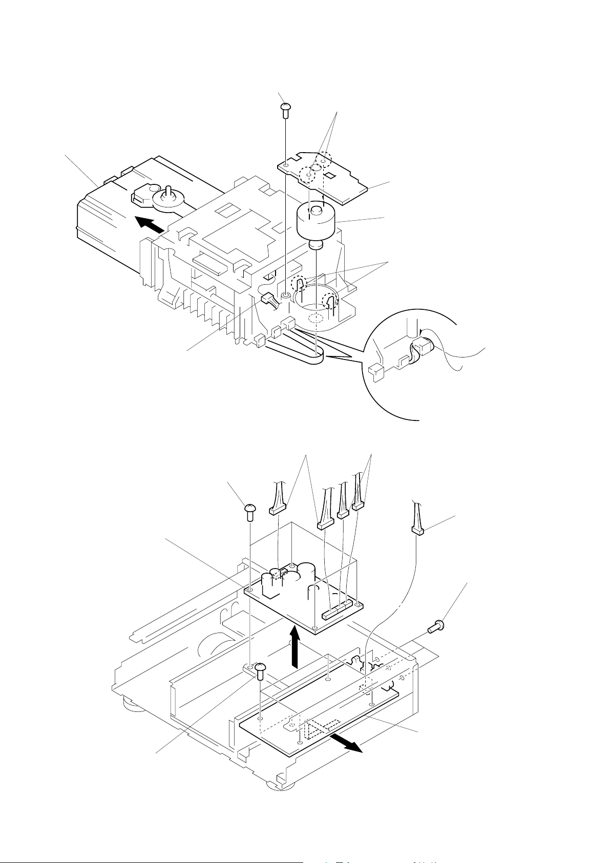
LOADING MOTOR
1
Pull the tray.
2
connector
(CN103)
4
screw
(BVTP 3
×
8)
7
Removal the two
solders of loading motor.
8
5
6
LOADING MOTOR board
loading motor
two claws
POWER BOARD, MAIN BOARD
4
POWER board
3
four screws
(BVTT3
3
Hang the belt
1
two connectors
(CN207, 309)
×
6)
2
two connectors
(CN203, 204)
5
connector
(CN302)
6
three screws
(BV/RING)
7
four screws
(BVTT3
8
Removal the MAIN board
A
×
6)
to direction of the arrow
A
.
– 18 –

SECTION 4
TEST MODE
4-1. AF MODE
Connect the TP19 (AFADJ) on the BD board to the ground and
turn on the power supply.
The AF mode is then activated and the following check can be
made.
4-1-1. Fluorescent Indicator Tube Check
After confirming display of all on, keep pressing the following
button, and the following display is attained.
p (STOP) button
(Display: 01)
” (PLAY) button
(Display: 02)
P (PAUSE) button
(Display: 03)
) button
SHUFFLE
0 button
PROGRAM
REPEAT
AUTO SPACE
STEP
INDEX
A-
EDIT
–
1
B
PEAK
(Display: 04)
(JUST)
(Display: 05)
Keep pressing the §OPEN/CLOSE button, and all on display is
attained again.
4-1-2. Key Check
All buttons are assigned with numbers respectively , and when each
button is pressed, it is counted and its number is displayed. Up to
“16” can be counted.
A button pressed once is not further counted but the number is
displayed. (Table 4-1)
(
count display
button number
display
(
Table 4-1.
Button Display Button Display
ERASE 00 P 03
EDIT/
TIME FADE
12 ) 04
FILE 13 0 05
FILTER 20 CHECK 06
ENTER 23 CLEAR 07
6 all light
OPEN/CLOSE up
P MODE 09
p 01 REPEAT 10
( 02 TIME 11
4-1-3. Remote Commander Check
Press the ( button on remote commander, and “ ˚ ” ( on the
set turn on. Nothing will be displayed if pressing another button.
CHECK button
CLEAR button
135
79
11 13 15
(Display: 06)
24
6810
12 14 ”
(Display: 07)
– 19 –

4-2. ADJ MODE
Connect the TP18 (ADJ) on the BD board to the ground and turn
on the power supply. The ADJ mode is then activated and the
following operation is executed.
• There is no problem even if Guarded Frame Sync is low value
continuously during playing.
• Do not perform high speed search during an access.The gain of
focus servo and spindle servo does not lower during playing.
• Manual operation and measurement of the servo system are possible. (For detailed operating method, see Table 4-2. in ADJ
Mode.)
Connecting Location:
[BD BOARD] (SIDE B)
CN107
TP19
(AFDJ)
TP18
(ADJ)
2
IC361
1
4-2-1. Button Operation Table in ADJ Mode
After all music numbers are displayed, press the TIME button,
and the jitter display mode is then set. The button functions are as
listed below.
Button Functions (Operate with remote commander.)
Table 4-2.
Button No. Test Mode
3 Tracking servo off
8 Tracking servo on
11 S-curve measuring mode
12 All servo off
13 Top turnblack display
14 Botton turnblack display
15 Center display
16 Optimum point display
17 Optimum jitter display
18 TE traverse display
19 VC, FE and RF display
20
Autogain display
(Focus, tracking and sled)
* For button numbers 3, 8, 11, and 12, use them only when an
oscilloscope is connected.
IC102
CN101
IC104
4-3. CLV-S MODE
The spindle servo can be operated for play in the CLV-S mode by
connecting TP18 (ADJ) and after turning on the power supply.
4-4. RELEASE THE TEST MODE
Disconnect the lead wire of test point connected in first step.
– 20 –

SECTION 5
ELECTRICAL ADJUSTMENTS
Notes:
1. CD block basically constructed to operate without adjustment.
Therefore, check each item in order given.
2. Use YEDS-18 disc (Part No.: 3-702-101-01) unless otherwise
indicated.
3. Use the oscilloscope with more than 10 MΩ impedance.
4. Clean an object lens by an applicator with neutral detergent
when the signal level is low than specified value with the following checks.
S-Curve Check
Connection:
BD board
TP2 (FE)
TP (VC)
Procedure:
1. Connect the oscilloscope to TP2 (FE) and TP (VC) on BD
board.
2. Connect the TP3 (FEI: IC101 pin @ª) and TP (VC) with lead
wire.
3. Turned power switch on.
4. Put disc (YEDS-18) in and turned power switch on again and
actuate the focus search. (actuate the focus search when disc
table is moving in and out.)
5. Confirm that the oscilloscope waveform (S-curve) is symmetrical between A and B. And confirm peak to peak level within
3.0 ± 1.0 Vp-p.
S-curve waveform
6. After check, remove the lead wire connected in step 2.
Note: • Try to measure several times to make sure that the ratio
of A : B or B : A is more than 10 : 7.
• Take sweep time as long as possible and light up the
brightness to obtain best waveform.
RF Level Check
Connection:
BD board
TP1 (RF)
TP (VC)
Procedure:
1. Connect the oscilloscope to TP1 (RF) and TP (VC) on BD
board.
2. Turned power switch on. (stop mode)
3. Put disc (YEDS-18) in and press the ( button.
4. Confirm that the oscilloscope waveform is clear and check RF
signal level is correct or not.
Note: Clear RF signal waveform means that the shape “≈” can
be clearly distinguished at the center of the waveform.
oscilloscope
+
–
symmetry
A
B
oscilloscope
(AC range)
+
–
within 3.0 ± 1.0 Vp-p
RF signal waveform
When observing the eye pattern, set the oscilloscope for A C range
and raise vertical sensitivity.
E-F Balance (Traverse) Check
Connection:
BD board
TP4 (TE)
TP (VC)
Procedure:
1. Connect the TP18 (ADJ) to ground and TP5 (TEI: IC101 pin
@¶) to TP (VC)with lead wire.
2. Connect the oscilloscope to TP4 (TE) and TP (VC) on BD
board.
3. Turned power switch on.
4. Put disc (YEDS-18) in and press the ( button.
5. Confirm that the oscilloscope waveform is symmetrical on the
top and bottom in relation to A Vdc, and check this level.
Traverse waveform
×
100 is ± 20 % or less.
A/B
oscilloscope
(DC range)
VOLT/DIV: 200 mV
TIME/DIV: 500 ns
(with the 10: 1 probe
in use)
level: 1.2 Vp-p
+
–
A
B
level: 1.3 ± 0.7 Vp-p
+0.25
–0.20
Symmetry
6. After check, remove the lead wire connected in step 1.
RF PLL Free-run Frequency Check
Connection:
BD board
TP13 (XPLCK)
Procedure:
1. Connect the frequency counter to TP13 (XPLCK).
2. Turned power switch on.
3. Put disc (YEDS-18) in and press the ( button.
4. Confirm that the reading on frequency counter is 4.3218 MHz.
frequency counter
+
–
Connecting Location:
[BD BOARD] (SIDE B)
TP13
(XPLCK)
CN107
CN101
TP1
(RF)
TP5
(TEI)
TP (VC)
TP3 (FEI)
TP2 (FE)
TP4
(TE)
TP18
(ADJ)
IC361
IC102
IC104
– 21 –
– 22 –

SECTION 6
DIAGRAMS
6-1. IC PIN FUNCTION DISCRIPTION
BD BOARD IC101 CXD2545Q
(DIGITAL SIGNAL PROCESSOR, FOCUS/TRACKING/SLED SERVO, EFM COMPARATOR)
Pin No. Pin Name I/ O Function
1 SRON O Sled servo drive PWM signal output terminal Not used (open)
2 SRDR O Sled servo drive PWM signal (–) output to the BA6297AFP (IC102)
3 SFON O Sled servo drive PWM signal output terminal Not used (open)
4 TFDR O Tracking servo drive PWM signal (–) output to the BA6297AFP (IC102)
5 TRON O Tracking servo drive PWM signal output terminal Not used (open)
6 TRDR O Tracking servo drive PWM signal (+) output to the BA6297AFP (IC102)
7 TFON O Tracking servo drive PWM signal output terminal Not used (open)
8 FFDR O Focus servo drive PWM signal (+) output to the BA6297AFP (IC102)
9 FRON O Focus servo drive PWM signal output terminal Not used (open)
10 FRDR O Focus servo drive PWM signal (–) output to the BA6297AFP (IC102)
11 FFON O Focus servo drive PWM signal output terminal Not used (open)
12 VCOO O Oscillator circuit output terminal for analog PLL of the playback EFM Not used (open)
13 VCOI I Oscillator circuit input terminal for analog PLL of the playback EFM Not used (fixed at “L”)
14 TEST I Input terminal for the test (fixed at “L”)
15 DVSS — Ground terminal (digital system)
16 TES2 I Input terminal for the test (fixed at “L”)
17 TES3 I Input terminal for the test (fixed at “L”)
18 PDO O Charge-pump output terminal for analog PLL of the playback EFM Not used (open)
19 VPCO O PLL charge-pump output terminal for the variable pitch Not used (open)
20 VCKI I Clock signal input from external VCO for the variable pitch Not used (fixed at “L”)
21 AVD2 — Power supply terminal (+5V) (analog system)
22 IGEN I Power supply terminal (+5V) (for operational amplifier)
23 AVS2 — Ground terminal (analog system)
24 ADII I Input terminal for the A/D converter Not used (open)
25 ADIO O Output terminal of the operational amplifier Not used (open)
26 RFDC I RF signal (DC level) input terminal for the digital servo process
27 TE I Tracking error signal input from the RF amplifier in optical pick-up
28 SE I Sled error signal input from the RF amplifier in optical pick-up
29 FE I Focus error signal input from the RF amplifier in optical pick-up
30 VC I Middle point voltage (+2.5V) input from the RF amplifier in optical pick-up
31 FILO O Filter output terminal for master clock of the playback master PLL
32 FILI I Filter input terminal for master clock of the playback master PLL
33 PCO O Phase comparison output terminal for master clock of the playback EFM master PLL
34 CLTV I Internal VCO control voltage input of the playback master PLL
35 AVS1 — Ground terminal (analog system)
36 RFAC I RF signal (AC level) input terminal for the EFM demodulator
37 BIAS I Constant current input terminal of the playback EFM asymmetry circuit
38 ASYI I Playback EFM asymmetry comparator voltage input terminal
39 ASYO O
40 AVD1 — Power supply terminal (+5V) (analog system)
41 DVDD — Power supply terminal (+5V) (digital system)
42 ASYE I Playback EFM asymmetry circuit on/off selection input terminal (fixed at “H”)
43 PSSL I Audio data output mode selection input terminal (fixed at “L”)
Playback EFM full-swing output terminal
Pin No. Pin Name I/ O Function
44 WDCK O Word clock signal (88.2 kHz) output terminal Not used (open)
45 LRCK O L/R sampling clock signal (44.1 kHz) output to the CXD8595Q (IC301)
46 DATA O
47 BCLK O
48 64 DATA O
4 9 64 BCLK O
5 0 64 LRCK O
51 GTOP O
52 XUGF O
53 XPLCK O
54 GFS O
55 RFCK O
56 C2PO O
57 XRAOF O
58 MNT3 O
59 MNT2 O
60 MNT1 O
61 MNT0 O
62 XTAI I System clock input terminal (16 MHz)
63 XTAO O System clock output terminal (16 MHz) Not used (open)
64 XTSL I System clock selection input terminal (fixed at “L”)
65 DVSS — Ground terminal (digital system)
66 FSTI I 2/3 divider input terminal of pins ^™ (XATI) and ^£ (XTAO)
67 FSTO O 2/3 divider output terminal of pins ^™ (XATI) and ^£ (XTAO)
68 C4M O 4.2336 MHz clock signal output terminal Not used (open)
69 C16M O 16.9344 MHz clock signal output terminal Not used (open)
70 MD2 I Digital out on/off control signal input from the system controller (IC351)
71 DOUT O Digital signal (for coaxial out and optical out) output terminal
72 EMPH O Emphasis control signal output terminal Not used (open)
73 WFCK O Write frame clock signal output terminal Not used (open)
74 SCOR O Sub-code sync (S0+S1) detection signal output to the system controller (IC351)
DA16 output when PSSL=“H”, 48-bit slot serial data output when PSSL=“L”
(PSSL (pin $£)=fixed at “L”) Serial data output to the CXD8595Q (IC301)
DA15 output when PSSL=“H”, 48-bit slot bit clock signal output when PSSL=“L”
(PSSL (pin $£)=fixed at “L”) Bit clock signal (2.8224 MHz) output to the CXD8595Q (IC301)
DA14 output when PSSL=“H”, 64-bit slot serial data output when PSSL=“L”
(PSSL (pin $£)=fixed at “L”) Not used (open)
DA13 output when PSSL=“H”, 64-bit slot bit clock signal output when PSSL=“L”
(PSSL (pin $£)=fixed at “L”) Not used (open)
DA12 output when PSSL=“H”, 64-bit slot L/R sampling clock signal output when PSSL=“L”
(PSSL (pin $£)=fixed at “L”) Not used (open)
DA11 output when PSSL=“H”, GTOP signal output when PSSL=“L”
(PSSL (pin $£)=fixed at “L”) Not used (open)
DA10 output when PSSL=“H”, XUGF signal output when PSSL=“L”
(PSSL (pin $£)=fixed at “L”) Not used (open)
DA09 output when PSSL=“H”, XPLCK signal output when PSSL=“L”
(PSSL (pin $£)=fixed at “L”) Not used (open)
DA08 output when PSSL=“H”, GFS (guard frame sync) signal output when PSSL=“L”
(PSSL (pin $£)=fixed at “L”) Not used (open)
DA07 output when PSSL=“H”, RFCK (read frame clock) signal output when PSSL=“L”
(PSSL (pin $£)=fixed at “L”) Not used (open)
DA06 output when PSSL=“H”, C2PO signal output when PSSL=“L”
(PSSL (pin $£)=fixed at “L”) Not used (open)
DA05 output when PSSL=“H”, XRAOF (RAM over flow) signal output when PSSL=“L”
(PSSL (pin $£)=fixed at “L”) Not used (open)
DA04 output when PSSL=“H”, MNT3 (monitor 3) signal output when PSSL=“L”
(PSSL (pin $£)=fixed at “L”) Not used (open)
DA03 output when PSSL=“H”, MNT2 (monitor 2) signal output when PSSL=“L”
(PSSL (pin $£)=fixed at “L”) Not used (open)
DA02 output when PSSL=“H”, MNT1 (monitor 1) signal output when PSSL=“L”
(PSSL (pin $£)=fixed at “L”) Not used (open)
DA01 output when PSSL=“H”, MNT0 (monitor 0) signal output when PSSL=“L”
(PSSL (pin $£)=fixed at “L”) Not used (open)
– 23 –
– 24 –

Pin No. Pin Name I/O Function
75 SBSO O Sub-code P-W serial data output terminal Not used (open)
95
96
97
98
76 EXCK I Sub-code P-W serial data reading clock signal input terminal Not used (fixed at “L”)
77 SUBQ O Sub-code Q data signal output to the system controller (IC351)
78 SQCK I Sub-code Q data reading clock signal input from the system controller (IC351)
79 MUTE I Mute signal input from the system controller (IC351)
80 SENS O Internal status (SENSE) signal output to the system controller (IC351)
81 XRST I
82 DIRC I 1-track jump mode input terminal Not used (fixed at “H”)
83 SCLK I Sense serial data reading clock signal input from the system controller (IC201)
84 DFSW I Defect on/off select signal input terminal Not used (fixed at “L”)
85 ATSK I Input terminal for the anti-shock Not used (fixed at “L”)
86 DATA I Serial data input from the system controller (IC351)
87 XLAT I Serial data latch pulse signal input from the system controller (IC351)
88 CLOK I Serial data transfer clock signal input from the system controller (IC351)
89 COUT O Track number count signal output terminal Not used (open)
90 DVDD — Power supply terminal (+5V) (digital system)
91 MIRR O Mirror detection signal output terminal Not used (open)
92 DFCT O Defect signal output terminal Not used (open)
93 FOK O Focus OK signal output terminal Not used (open)
94 FSW O Selection signal output terminal of the output filter for spindle motor Not used (open)
MON O Spindle motor on/off control signal output terminal Not used (open)
99 SSTP I
100 SFDR O Sled servo drive PWM signal (+) output to the BA6297AFP (IC102)
MDP O Spindle servo control signal output terminal
MDS O Spindle servo control signal output terminal Not used (open)
LOCK O
System reset signal input from the reset signal generator (IC206) “L”: reset
For several hundreds msec. after the power supply rises, “L” is input, then it changes to “H”
GFS is sampled by 460 Hz “H” output when GFS is “H” Not used (open)
Detection input from the sled limit-in detect switch (SW102)
The optical pick-up is inner position when “H”
– 25 –

• BD BOARD IC351 CXP84124-068Q (SYSTEM CONTROL)
Pin No. Pin Name I/O Function
1A3O
2A4O
3A5O
4A6O
5A7O
6A8O
7A9O
8 A10 O
9 A11 O
10 A12 O
11
12
13 NC O Not used (open)
14 LED-PLAY O
15 LED-PAUSE O
16 LED-FILTER O FILTER LED (D873) drive signal output terminal “H”: LED on
17 SPDL-MUTE O Mute signal output to the spindle motor driver (IC102, 104)
18 SHIFT-ON/OFF O
19 VOL UP O Volume up control signal output to the volume control motor driver (IC354)
20 VOL DOWN O Volume down control signal output to the volume control motor driver (IC354)
21
22
23
24
WE O Write enable signal output to the static RAM (IC352)
NC O Not used (open)
BLANK O Blank signal output to the fluorescent indicator tube driver (IC801 to IC803)
FL D0 O Serial data output to the fluorescent indicator tube driver (IC803)
FL D1 O Serial data output to the fluorescent indicator tube driver (IC802)
FL D2 O Serial data output to the fluorescent indicator tube driver (IC801)
Address signal output to the static RAM (IC352)
( LED (D871) drive signal output terminal “H”: LED on
P LED (D872) drive signal output terminal “H”: LED on
Reset signal output to the CXD2562Q-CS (IC302) “L”: reset
25
26
27 SENSER SW O
28 SENSER I Detect signal input from the stabilizer detect sensor (IC361) “H”: on
29
30
31
32
33
34
35
36
37
38 ADJ/AFADJ I Setting terminal for the test mode “L” active
39
40
41 K2 I
FL CLK O Serial data transfer clock signal output to the fluorescent indicator tube driver (IC801 to IC803)
FL WR O Read/write select signal output to the fluorescent indicator tube driver (IC801 to IC803)
On/off control signal output to the stabilizer detect sensor (IC361) “H”: on
LIMIT OUT I
RESET I
XTALI I Main system clock input terminal (4 MHz)
XTALO O Main system clock output terminal (4 MHz)
VSS — Ground terminal
TX O Sub system clock output terminal Not used (open)
TEX I Sub system clock input terminal Not used (fixed at “L”)
AVSS — Ground terminal (for A/D converter)
AVREF I Reference voltage input terminal (+5V)
K0 I Key input terminal (A/D input) (fixed at “H”)
K1 I
Detection input from the sled limit-out detect switch
The optical pick-up is outer position when “L” Not used (fixed at “L”)
System reset signal input from the reset signal generator (IC206) “L”: reset
For several hundreds msec. after the power supply rises, “L” is input, then it changes to “H”
Key input terminal (A/D input)
P MODE, TIME keys (S819S820) input
Key input terminal (A/D input)
ERASE, CHECK, CLEAR, FILTER, 0, ) , keys (S801 to S806) input
– 26 –

Pin No. Pin Name I/O Function
42 K3 I
n
Key input terminal (A/D input) EDIT/TIME FADE, REPEAT, FILE,
§ OPEN/CLOSE, (, P, p keys (S811 to S817) input
43 K4 I
44 K5 I
45 IN/OUT SW I Detection input from the loading in/out detect switch (S281, S282) (A/D input)
46 SCLK O Sense serial data reading clock signal output to the CXD2545Q (IC101)
47 PRGL O Serial data latch pulse signal output to the CXD8595Q (IC301)
48 CLK O Serial data transfer clock signal output to the CXD2545Q (IC101) and CXD8595Q (IC301)
49 SENSE I Internal status (SENSE) signal input from the CXD2545Q (IC101)
50 DATA O Serial data output to the CXD2545Q (IC101) and CXD8595Q (IC301)
51 SQCK O Sub-code Q data reading clock signal output to the CXD2545Q (IC101)
52 SUBQ I Sub-code Q data signal input from the CXD2545Q (IC101)
53 TEST O Output terminal for the test Not used (open)
54 SEL1 I Destination setting terminal (fixed at “L”)
55 SEL0 I Destination setting terminal (fixed at “L”)
56 RMIN I Remote control signal input from the remote control receiver (IC804)
57 TIMER I Timer control input terminal Not used (fixed at “H”)
58 TEST O Output terminal for the test Not used (open)
59 TEST O Output terminal for the test Not used (open)
60 SCOR I Sub-code sync (S0+S1) detection signal input from the CXD2545Q (IC101)
61 AMUTE O Muting control signal output to the analog mute driver and mute relay driver
62 LDON O Laser diode on/off selection signal output to the RF amplifier in optical pick-up
63 XLT O Serial data latch pulse signal output to the CXD2545Q (IC101)
64 LOAD OUT O Loading motor (M2) drive signal output to the NJM4558 (IC182) *1
65 LOAD IN O Loading motor (M2) drive signal output to the NJM4558 (IC182) *1
66 DOUT O Digital out on/off control signal output to the CXD2545Q (IC101) Not used (Open)
67 DMUTE O Muting control signal output to the CXD2545Q (IC101) and CXD8595Q (IC301)
68 D0 I/O
69 D1 I/O
70 D2 I/O
71 D3 I/O
72 VDD — Power supply terminal (+5V)
73 NC I Not used (fixed at “H”)
74 D4 I/O
75 D5 I/O
76 D6 I/O
77 D7 I/O
78 A0 O
79 A1 O Address signal output to the static RAM (IC352)
80 A2 O
Rotary encoder input terminal (A/D input) AMS ± key (RV801) input
Rotary encoder input terminal (A/D input) AMS ≠ key (RV801) input
Two-way data bus with the static RAM (IC352)
Two-way data bus with the static RAM (IC352)
*1 Loading motor (M2) control
Operatio
Terminal
LOAD OUT (pin ^¢)
LOAD IN (pin ^∞)
OFF OUT I N BRAKE
“L” “H” “L” “H”
“L” “L” “H” “H”
– 27 –

Main Ports
d
n
d
SPDL-MUTE (pin !¶)
From the viewpoint of performance of the set, the disc must
not move nor sway when the disc table opens. These
problems however occur in the actual case due to the offset
voltage generated and the voltage generated because of the
positional relation between the BSL coil and Hall element.
The spindle motor driver (IC102, IC104) is therefore mute
while the tray is open. Pin !¶ provides the timing for this.
H
SP MUTE
SENSER SW (pin @¶)
As IC361 IS471F operate in pulse as shown i n the figure, the
sound quality may be affected if operated constantly. As the
purpose of IC361 is to detect if the presence of the stabilizer,
it should be operated only when the tray is drawn in. IC361
operates as it is “H” only at this time. Normally it is “L”.
Eep
Ee
Eed
L
(MUTE ON)
OPEN
Reverses after a
certain period of time.
CLOSE SPINDLE
Reverses after a
certain period of time.
Time while the
disc can be see
(Estimate).
PLAY
KICK
The spindle
motor driver is
muted during
this time.
BLANK (pin @¡)
This port is required because the display tube in this set static
lights up and a dedicated screwdriver is required. It is
basically a RESET pin. But as problems will occur if u se
also a s RESET, timings are specially provided using t he
micro-processor.
0
GLout pin
output waveform
Eepis the luminance of the signal light tuned with the low
*
Time
level timing of the GLout pin output.
Eedis the luminance of the D.C. light. Th e light source is
the infrated-emitting diode (λp=940 nm).
SENSER (pin @•)
The results of the detection of IC361 IS471F is output to this
pin. It becomes “ L ” when there is no stabilizer (when light
reaches). The next process of imposing the next focus is not
performed. (Effective only when pin @¶ is “H”.)
Therefore, it must be noted that if PLAY is performed when th
servo board a t the top of the CDM is not assembled properly,
the detection circuit operates and this pin does not operate.
It is does not operate, refer to 1. SERVICING NOTES ” Preparations for Adjustment and Measurement” on page 3.
– 28 –

• IC Block Diagrams
– BD Section –
IC103 CXA1821M
VEE
1
LD
VCC
PD
2
A
3
B
4
C
5
D
6
7
F
8
E
9
10
EI
VEE
+
–
VC
RF SUMMING AMP
+
–
+
–
VREF
VEE
–
+
VC
VEE
VC
VC
+
–
APC LD AMP
–
+
FOCUS ERROR AMP
VC
VC
VCC
VEE
RF EQ AMP
VC
TRACKING ERROR AMP
–
+
VC BUFFER
+
–
VCC
–
+
20
VCC
LD ON
19
LC/PD
18
RFE
17
RFO
16
15
FE
FE BIAS
14
TE
13
VC
VC
12
EO
11
IC181 TA7256P
+
–
2 345 6 7 8 9 10
1
VEE
–IN1
+IN1
+IN2
OUT1
SENSE1
–IN2
+
–
VCC
OUT2
SENSE2
– 29 –

– MAIN Section –
IC206 M51957AL
–
+
1.25V
1 2
VDD
3
IN
GND
IC301 CXD8595Q
NRGCLR
51 50 49 48 47 46 45 44
IF SELD
52
IF SELC
53
54
NC
55
SBCKI
SDATAR
SDATAL
DFDTOL
DFBCKO
DFDTEN
TEST1
TEST2
VSS
4BIT DATA
56
BITSTREAM
57
58
NC
59
60
61
62
63
64
4
DL
SYSM
LATCH
ATT
IIR
OVERFLOW DETECTOR
5
OUT
SHIFT
MODE
FIR 4
FIR 2FIR 1 FIR 3
P/S CONVERT
D/F-CLK GEN.
ATT
INIT
LRCKI
DATAI
BCKI
VSS
VSS
NC
INVO2
INVO1
INVI
NC
128FSO
CKVDD
DINIT
42
43
TIMING
CIRCUIT
S / P
ATT
IIR
FIR 4
FIR 2FIR 1 FIR 3
OVERFLOW DETECTOR
&
40 39 38 37 36 35 34 33
41
ATT
x 0.75
ATT
x 0.75
POLALITY
OR
L . I . P.
DITHER
L . I . P.
"0" DETECT
CIRCUIT
CLOCK
GENERATOR
MUTE
3rd order
NOISE
SHAPER
3rd order
NOISE
SHAPER
32
31
30
29
28
27
26
25
24
23
22
21
20
INAF
OVFLAG
MUTER
MUTEL
MTPOL
DRPOL
MODE
NC
DFDTOR
DFLRCKO
TEST4
TEST3
VSS
1 2
PLMG2
VDD
3
NSDOL4
DATA SELECT
4
5
NSDOL3
NSDOL2
6
NSDOL1
2
8
7
NC
NC
9 10
VDD
VDD
12 13
11
NC
64FSI
DATA SELECT
NSDOR1
14
NSDOR2
15 16 17
NSDOR3
NSDOR4
MCKIN
18 19
VDD
PLMG1
– 30 –

IC302 CXD2562Q
DPO/BCKO
DM2/SDRO
DM1/SDLO
DLO
51 50 49 48 47
DRO
LRCKO
INAF
DINIT
43444546
128FS
DVSSL
DVSSR
512FSO
BCKI
DLI
DRI
LRCKI
MUTEL
MUTER
33343536373839404142
INIT
DATAOUT
52
ON/OFF
TEST1
53
54
TEST2
55
TEST3
DVDDL
56
VSUB (D) L
VSUB (CHIP) L
VDD2
VDD
L1 (–)
VSS
L1 (+)
VSS2
57
58
59
60
61
62
63
64
IC354 BA6208
INTERPOLATER
INTERPOLATER
THIRD ORDER
NOISE SHAPER
THIRD ORDER
NOISE SHAPER
2 345 6 7 8 9
1
VSS
VSS2
L2 (+)
L2 (–)
VDD
VDD2
CLOCK
GENERATOR
XVDD
VSUB (A) L
TIMING CIRCUIT
10
11
XIN
XOUT
PLM
PLM
XVSS
XVSS
VDD2
VSUB (A) R
VDD
R2 (–)
S/P
VSS
1918171615141312
R2 (+)
VSS2
32
SYNC
31
COEF
SPLM
30
18/20
29
DVDDR
28
27
VSUB (D) R
VSUB (CHIP) R
26
VDD2
25
VDD
24
R1 (–)
23
VSS
22
R1 (+)
21
VSS2
20
GND
MOTOR
DRIVE
MOTOR
DRIVE
REG
Vcc
SWITCH
SWITCH
1 2 3 4 5 6 7
NC
INPUT 1
NC
INPUT 2
OUTPUT 2
8
OUTPUT1
9
NC
– 31 –

IC501, 601 CXA8042AS
1
I01+
2
I02–
3
NC
4
I01–
5
I02+
6
NC
7
VCC2
8
C2
C1
9
10
VCC1
VREF
VCNT
GND1
RIREF
REFERENCE
11
12
13
14
VOLTAGE
CIRCUIT
– PANEL Section –
IC801, 802, 803 LC7570E
SWITCHING
CIRCUIT
CONSTANT
CURRENT
CIRCUIT
CONTROL
CIRCUIT
28
IN2–
27
IN2+
26
NC
25
IN1+
IN1–
24
NC
23
C4
22
C3
21
GND2
20
VEE2
19
18
VEE1
17
C6
C5
16
15
CIREF
BLK
VSS
SIN
S33
S32
S31
S30
S29
S28
S27
S26
NC
VDA
DATACLWR
464748 45 44 43 42 41 40 39 38 37
1
NC
2
3
4
5
6
7
8
9
10
11
12
13
14
NC
S25
SHIFT REGISTER
A/D CONVERTER
LATCH, FL DRIVER
15
16
S24
VFLS0S1S2S3NCS4
17 181920 21 22 23
S22
S21NCS20
S23
S19
S18
S17
36
S5
35
S6
34
S7
33
S8
32
S9
31
S10
30
S11
29
S12
28
S13
27
S14
26
S15
25
S16
24
NC
– 32 –

• Wave forms
– MAIN BOARD –
1 IC302 !º (XIN)
45.455 MHz
– BD BOARD –
2 IC351 #™ (XOUT)
4.00 MHz
2.02 Vp-p
5.92 Vp-p
6 IC101 $∞ (LRCK)
44.053 kHz
7 IC101 #§ (RFAC)
200 mV/DIV, 500 nS/DIV
6.32 Vp-p
+0.25
1.25 Vp-p
–0.20
3 IC101 %£ (XPLCK)
4.310 MHz
4 IC101 %∞ (RFCK)
7.353 kHz
6.8 Vp-p
5.84 Vp-p
8 IC101 @ª (FE)
0.1 Vp-p
9 IC101 @¶ (TE)
8.4 Vp-p
5 IC101 $¶ (BCLK)
2.1186 MHz
!º IC101 (§ (MDP)
3.6Vp-p
6.24 Vp-p
131.58 kHz
– 33 –

• Circuit Boards Location
BD board
VOL SEL board
POWER board
DISPLAY board
POWER SW board
HP board
BD TRANSLA TION board
PANEL board
LOADING MOTOR board
LOADING SW board
MAIN board
BSL board
– 34 –


SECTION 7
EXPLODED VIEWS
NOTE:
• -XX and -X mean standardized parts, so they
may have some difference from the original
one.
• Color Indication of Appearance Parts
Example:
KNOB, BALANCE (WHITE)
↑
Cabinet's Color
(1) CASE, LOADING PANEL SECTION
10
• Items marked “*” are not stocked since they
are seldom required for routine service. Some
delay should be anticipated when ordering
these items.
• The mechanical parts with no reference num-
ber in the exploded views are not supplied.
• Hardware (# mark) list and accessories and
packing materials are given in the last of the
electrical parts list.
8
9
The components identified by mark
! or dotted line with mark ! are
critical for safety.
Replace only with part number
specified.
11
not supplied
10
#1
12
not
supplied
#1
8
front panel
8
10
7
5
#1
#1
6
4
not supplied
3
not supplied
1
2
Ref. No. Part No. Description Remark Ref. No. Part No. Description Remark
1 3-703-685-21 SCREW (+BV 3X8)
2 4-970-998-21 BOLT (LID), HEXAGON HOLE (GOLD)
2 4-970-998-31 BOLT (LID), HEXAGON HOLE (BLACK)
3 4-987-965-01 EMBLEM (FIXED PICKUP) (GOLD)
3 4-987-965-11 EMBLEM (FIXED PICKUP) (BLACK)
4 4-986-744-01 PANEL, LOADING (GOLD)
4 4-986-744-11 PANEL, LOADING (BLACK)
5 4-986-745-01 BASE, LOADING PANEL (GOLD)
5 4-986-745-11 BASE, LOADING PANEL (BLACK)
6 1-777-844-11 WIRE (FLAT TYPE) (9 CORE)
7 1-777-845-11 WIRE (FLAT TYPE) (10 CORE)
8 4-959-077-01 DAMPER
* 9 4-615-354-01 SPACER
10 3-363-099-01 SCREW (CASE 3 TP2) (BLACK)
10 3-363-099-11 SCREW (CASE 3 TP2) (GOLD)
11 4-969-469-01 CASE (BLACK)
11 4-969-469-31 CASE (GOLD)
* 12 4-962-329-01 DAMPER
– 61 –

(2) FRONT PANEL SECTION
59
62
59
53
52
#2
54
57
55
56
58
supplied with
J401
not supplied
74
73
59
60
59
64
supplied with
VR405
65
66
61
68
67
70
59
63
59
69
supplied with RV801
71
72
51
Ref. No. Part No. Description Remark Ref. No. Part No. Description Remark
51 4-987-121-01 KNOB (AMS) (GOLD)
51 4-987-121-11 KNOB (AMS) (BLACK)
52 4-950-189-01 KNOB (A) (VOL) (BLACK)
52 4-950-189-41 KNOB (A) (VOL) (GOLD)
53 4-942-568-01 EMBLEM (NO.5), SONY (BLACK)
53 4-942-568-31 EMBLEM (NO.5), SONY (GOLD)
54 4-986-664-01 PANEL, FRONT (GOLD)
54 4-986-664-11 PANEL, FRONT (BLACK)
55 4-986-670-01 PLATE, INDICATION
56 4-986-666-01 BASE (L), PANEL (GOLD)
56 4-986-666-11 BASE (L), PANEL (BLACK)
57 4-923-520-51 KNOB, POWER (POWER) (BLACK)
57 4-923-520-61 KNOB, POWER (POWER) (GOLD)
* 58 1-663-575-12 POWER SW BOARD
59 4-951-620-01 SCREW (2.6X8), +BVTP
* 60 A-4699-566-A HP BOARD, COMPLETE (BLACK)
* 60 A-4699-710-A HP BOARD, COMPLETE (GOLD)
61 4-986-669-01 FILTER
* 62 A-4699-353-A DISPLAY BOARD, COMPLETE
63 4-986-668-01 BRACKET (PACKING)
#2
64 4-986-667-01 PACKING
65 4-986-687-01 BUTTON (P.MODE) (GOLD)
65 4-986-687-11 BUTTON (P.MODE) (BLACK)
66 4-986-671-01 BUTTON (2) (GOLD)
66 4-986-671-11 BUTTON (2) (BLACK)
67 4-986-672-01 BUTTON (3) (GOLD)
67 4-986-672-11 BUTTON (3) (BLACK)
68 4-986-673-01 BUTTON (FF) (0. )) (GOLD)
68 4-986-673-11 BUTTON (FF) (0. )) (BLACK)
* 69 A-4699-354-A PANEL BOARD, COMPLETE
* 70 3-362-478-01 HOLDER (T), LED
71 X-4945-276-1 BUTTON (PLAY) ASSY
(§ OPEN/CLOSE. (. P. p) (BLACK)
71 X-4948-030-1 BUTTON (PLAY) ASSY
(§ OPEN/CLOSE. (. P. p) (GOLD)
72 4-986-665-01 BASE (R), PANEL (GOLD)
72 4-986-665-11 BASE (R), PANEL (BLACK)
73 4-971-776-01 INDICATOR
74 4-949-302-21 WASHER
– 62 –

(3) CHASSIS SECTION
mechanism deck
(CDM36A-14A)
104
not
supplied
114
T1
107
#1
not
supplied
not
supplied
#1
#1
not
supplied
not
supplied
#1
106
105
107
not supplied
#1
not supplied
#1
#1
not supplied
108
#1
not supplied
109
CNP1
#1
110
#1
111
#1
#1
#1
not supplied
not supplied
112
103
not supplied
#1
#1
113
103
#6
#1
#4
102
101
102
The components identified by mark
! or dotted line with mark ! are
101
Ref. No. Part No. Description Remark Ref. No. Part No. Description Remark
101 4-970-124-01 CUSHION (F50180S)
102 4-970-123-01 FOOT (F50180S)
103 4-984-485-01 CUSHION (FOOT)
* 104 1-663-576-13 VOL SEL BOARD
105 1-777-873-11 WIRE (FLAT TYPE) (16 CORE)
* 110 3-703-244-00 BUSHING (2104), CORD
111 3-704-515-21 SCREW (BV/RING)
* 112 4-986-682-11 PANEL, BACK (AEP)
* 112 4-986-682-22 PANEL, BACK (Singapore)
113 3-831-441-XX CUSHION, SPEAKER
critical for safety.
Replace only with part number
specified.
* 106 A-4699-712-A POWER BOARD, COMPLETE
107 4-985-057-01 WASHER
* 108 A-4699-567-A MAIN BOARD, COMPLETE
* 109 4-923-873-01 BRACKET, CORD STOPPER
114 1-543-653-11 CORE ASSY, BEAD (DIVISION TYPE)
! CNP1 1-558-568-21 CORD, POWER
! T1 1-431-214-11 TRANSFORMER, POWER (Singapore)
! T1 1-431-215-11 TRANSFORMER, POWER (AEP)
– 63 –

(4) MECHANISM DECK SECTION-1
(CDM36A-14A)
156
155
#2
#2
#2
not supplied
#2
not supplied
#2
#2
BU-14A
152
#2
#5
153
154
153
not supplied
158
not supplied
#2
159
161
160
#3
164
165
166
not supplied
168
162
163
167
#2
M2
not supplied
not supplied
151
Ref. No. Part No. Description Remark
* 151 4-977-889-01 PLATE (BU), GROUND
152 4-989-303-01 SPRING (BU-LF), COMPRESSION
153 4-988-104-01 SPRING (BU), COMPRESSION
* 154 4-986-917-01 COVER (F) (DRAWER)
155 4-986-916-01 PANEL (DRAWER)
* 156 4-986-918-01 COVER (R) (DRAWER)
* 157 4-977-888-01 SHAFT
* 158 4-977-892-01 BEARING
* 159 4-977-891-01 PLATE, GROUND
160 X-4924-457-1 ROLLER ASSY
161 4-934-376-01 SHAFT (ROLLER)
162 1-777-843-11 WIRE (FLAT TYPE) (30 CORE)
172
#2
171
169
157
170
Ref. No. Part No. Description Remark
* 163 A-4699-708-A BD BOARD, COMPLETE
164 4-977-897-01 GEAR
165 4-977-898-01 LEVER (SWING)
166 4-977-896-01 PULLEY
* 167 1-663-579-11 LOADING MOTOR BOARD
* 168 1-663-581-11 LOADING SW BOARD
169 4-968-905-01 BELT (CDM)
170 4-986-919-01 LIMITTER (LEVER)
171 4-988-103-01 SLIDER (SWING)
172 4-988-107-01 CUSHION (LD)
M2 A-4660-970-A MOTOR ASSY (LOADING)
– 64 –

(5) MECHANISM DECK SECTION-2
(BU-14A)
214
215
210
209
211
208
#6
not
supplied
#6
207
212
204
#7
213
205
220
207
218
216
217
211
219
221
203
M1
223
202
Ref. No. Part No. Description Remark
201 4-951-620-01 SCREW (2.6X8), +BVTP
* 202 1-663-580-11 BD TRANSLATION BOARD
203 A-4672-247-A BASE (OUTSERT) ASSY
204 4-977-921-01 GEAR (B), FLAT
* 205 4-977-918-01 BASE (OUTSERT)
206 4-977-920-01 GEAR (C), FLAT
207 4-917-562-11 INSULATOR
* 208 4-977-924-01 SPRING (OP), LEAF
209 1-775-991-11 WIRE (FLAT TYPE) (16 CORE)
! 210 8-848-379-31 OPTICAL PICK-UP KSS-213B/S-N
206
not supplied
201
201
Ref. No. Part No. Description Remark
213 4-977-925-01 SPRING (SLIDE BASE), COMPRESSION
214 4-968-871-01 WASHER (SPINDLE)
215 4-968-867-01 CAP, CENTERING
216 4-968-869-01 SPRING (CENTERING), COMPRESSION
217 A-4660-814-A PULLEY ASSY, DISK
218 4-971-266-01 SCREW (M2.6X4)
219 X-4947-796-1 BASE ASSY, SLIDE
220 X-4947-797-1 ROTOR ASSY
221 1-777-842-11 WIRE (FLAT TYPE) (10 CORE)
222 A-4699-360-A BSL BOARD, COMPLETE
The components identified by mark
! or dotted line with mark ! are
critical for safety.
Replace only with part number
specified.
222
211 4-977-923-01 SHAFT, SLED
212 4-977-926-01 RACK, SLIDE
223 X-4947-838-1 STABILIZER ASSY
M1 X-4947-303-1 MOTOR ASSY (SLED)
– 65 –

BD
SECTION 8
ELECTRICAL PARTS LIST
NOTE:
• Due to standardization, replacements in the
parts list may be different from the parts specified in the diagrams or the components used on
the set.
• -XX and -X mean standardized parts, so they
may have some difference from the original one.
• RESISTORS
All resistors are in ohms.
METAL: Metal-film resistor.
METAL OXIDE: Metal oxide-film resistor.
F: nonflammable
Ref. No. Part No. Description Remark
* A-4699-708-A BD BOARD, COMPLETE
*******************
< CAPACITOR >
C93 1-124-997-11 ELECT 470uF 20% 10V
C94 1-124-997-11 ELECT 470uF 20% 10V
C101 1-163-005-11 CERAMIC CHIP 470PF 10% 50V
C102 1-163-038-00 CERAMIC CHIP 0.1uF 25V
C103 1-163-005-11 CERAMIC CHIP 470PF 10% 50V
C104 1-163-145-00 CERAMIC CHIP 0.0015uF 5% 50V
C105 1-135-155-21 TANTALUM CHIP 4.7uF 10% 16V
C108 1-163-035-00 CERAMIC CHIP 0.047uF 50V
C109 1-163-145-00 CERAMIC CHIP 0.0015uF 5% 50V
C110 1-163-017-00 CERAMIC CHIP 0.0047uF 5% 50V
• Items marked “*” are not stocked since they
are seldom required for routine service.
Some delay should be anticipated when ordering these items.
• SEMICONDUCTORS
In each case, u: µ, for example:
uA. . : µA. . uPA. . : µPA. .
uPB. . : µPB. . uPC. . : µPC. .
uPD. . : µPD. .
• CAPACITORS
uF: µF
• COILS
uH: µH
The components identified by mark
! or dotted line with mark ! are
critical for safety.
Replace only with part number
specified.
When indicating parts by reference
number, please include the board.
Ref. No. Part No. Description Remark
C163 1-164-492-11 CERAMIC CHIP 0.15uF 10% 16V
C171 1-163-005-11 CERAMIC CHIP 470PF 10% 50V
C172 1-163-005-11 CERAMIC CHIP 470PF 10% 50V
C173 1-164-232-11 CERAMIC CHIP 0.01uF 50V
C175 1-163-038-00 CERAMIC CHIP 0.1uF 25V
C261 1-126-177-11 ELECT 100uF 20% 10V
C325 1-163-038-00 CERAMIC CHIP 0.1uF 25V
C351 1-125-622-11 CAPACITOR 0.1F 5.5V
C352 1-163-038-00 CERAMIC CHIP 0.1uF 25V
C360 1-163-038-00 CERAMIC CHIP 0.1uF 25V
C370 1-163-038-00 CERAMIC CHIP 0.1uF 25V
C371 1-163-038-00 CERAMIC CHIP 0.1uF 25V
C372 1-126-177-11 ELECT 100uF 20% 10V
C111 1-163-251-11 CERAMIC CHIP 100PF 5% 50V
C112 1-163-038-00 CERAMIC CHIP 0.1uF 25V
C113 1-163-038-00 CERAMIC CHIP 0.1uF 25V
C114 1-163-038-00 CERAMIC CHIP 0.1uF 25V
C115 1-124-673-11 ELECT 100uF 20% 10V
C116 1-124-673-11 ELECT 100uF 20% 10V
C117 1-126-209-11 ELECT 100uF 20% 4V
C118 1-163-275-11 CERAMIC CHIP 0.001uF 5% 50V
C119 1-163-231-11 CERAMIC CHIP 15PF 5% 50V
C122 1-164-336-11 CERAMIC CHIP 0.33uF 25V
C123 1-164-232-11 CERAMIC CHIP 0.01uF 50V
C124 1-164-005-11 CERAMIC CHIP 0.47uF 25V
C125 1-163-038-00 CERAMIC CHIP 0.1uF 25V
C126 1-164-489-11 CERAMIC CHIP 0.22uF 10% 16V
C127 1-163-038-00 CERAMIC CHIP 0.1uF 25V
C128 1-163-038-00 CERAMIC CHIP 0.1uF 25V
C131 1-164-346-11 CERAMIC CHIP 1uF 16V
C132 1-164-346-11 CERAMIC CHIP 1uF 16V
C140 1-163-038-00 CERAMIC CHIP 0.1uF 25V
C141 1-163-038-00 CERAMIC CHIP 0.1uF 25V
C151 1-163-005-11 CERAMIC CHIP 470PF 10% 50V
C152 1-163-005-11 CERAMIC CHIP 470PF 10% 50V
C153 1-163-038-00 CERAMIC CHIP 0.1uF 25V
C154 1-164-336-11 CERAMIC CHIP 0.33uF 25V
C155 1-163-005-11 CERAMIC CHIP 470PF 10% 50V
C156 1-163-005-11 CERAMIC CHIP 470PF 10% 50V
C157 1-163-023-00 CERAMIC CHIP 0.015uF 5% 50V
C158 1-163-023-00 CERAMIC CHIP 0.015uF 5% 50V
C161 1-163-038-00 CERAMIC CHIP 0.1uF 25V
C162 1-163-038-00 CERAMIC CHIP 0.1uF 25V
< CONNECTOR >
CN101 1-691-894-21 SOCKET, CONNECTOR 16P
* CN102 1-563-017-11 CONNECTOR, FPC 30P
* CN103 1-568-941-11 PIN, CONNECTOR 3P
* CN104 1-564-518-11 PLUG, CONNECTOR 3P
* CN105 1-564-518-11 PLUG, CONNECTOR 3P
CN106 1-568-853-11 SOCKET, CONNECTOR 10P
* CN107 1-568-852-11 SOCKET, CONNECTOR 9P
CN113 1-506-481-11 PIN, CONNECTOR 2P
< DIODE >
D101 8-719-016-74 DIODE 1SS352
D351 8-719-016-74 DIODE 1SS352
D361 8-719-938-07 DIODE GL480
< IC >
IC101 8-752-369-78 IC CXD2545Q
IC102 8-759-071-79 IC BA6297AFP
IC103 8-752-072-45 IC CXA1821M-T6
IC104 8-759-071-79 IC BA6297AFP
IC351 8-752-884-95 IC CXP84124-068Q
IC352 8-759-289-94 IC LH5160TF
IC361 8-749-010-61 IC IS471F
< COIL >
L101 1-414-234-11 INDUCTOR, FERRITE BEAD
– 66 –

BD
Ref. No. Part No. Description Remark
< TRANSISTOR >
Q101 8-729-010-08 TRANSISTOR MSB710-R
Q102 8-729-010-08 TRANSISTOR MSB710-R
Q103 8-729-424-18 TRANSISTOR UN2113-TX
Q104 8-729-421-19 TRANSISTOR UN2213
Q105 8-729-424-18 TRANSISTOR UN2113-TX
Q106 8-729-421-19 TRANSISTOR UN2213
Q301 8-729-424-08 TRANSISTOR UN2111
Q302 8-729-421-22 TRANSISTOR UN2211
< RESISTOR >
R101 1-216-077-00 METAL CHIP 15K 5% 1/10W
R102 1-216-097-00 METAL GLAZE 100K 5% 1/10W
R103 1-216-077-00 METAL CHIP 15K 5% 1/10W
R104 1-216-085-00 METAL CHIP 33K 5% 1/10W
R105 1-216-097-00 METAL GLAZE 100K 5% 1/10W
R106 1-216-061-00 METAL CHIP 3.3K 5% 1/10W
R107 1-216-061-00 METAL CHIP 3.3K 5% 1/10W
R108 1-216-073-00 METAL CHIP 10K 5% 1/10W
R109 1-216-121-00 METAL GLAZE 1M 5% 1/10W
R110 1-216-025-00 METAL GLAZE 100 5% 1/10W
R111 1-216-693-11 METAL CHIP 56K 0.5% 1/10W
R112 1-216-049-00 METAL GLAZE 1K 5% 1/10W
R113 1-216-073-00 METAL CHIP 10K 5% 1/10W
R114 1-216-073-00 METAL CHIP 10K 5% 1/10W
R115 1-216-677-11 METAL CHIP 12K 0.5% 1/10W
R116 1-216-695-11 METAL CHIP 68K 0.5% 1/10W
R117 1-216-073-00 METAL CHIP 10K 5% 1/10W
R118 1-216-073-00 METAL CHIP 10K 5% 1/10W
R119 1-216-097-00 METAL GLAZE 100K 5% 1/10W
R120 1-216-105-00 METAL GLAZE 220K 5% 1/10W
R121 1-216-073-00 METAL CHIP 10K 5% 1/10W
R122 1-216-073-00 METAL CHIP 10K 5% 1/10W
R123 1-216-073-00 METAL CHIP 10K 5% 1/10W
R124 1-216-097-00 METAL GLAZE 100K 5% 1/10W
R125 1-216-049-00 METAL GLAZE 1K 5% 1/10W
R126 1-216-049-00 METAL GLAZE 1K 5% 1/10W
R127 1-216-049-00 METAL GLAZE 1K 5% 1/10W
R131 1-216-037-00 METAL CHIP 330 5% 1/10W
R132 1-216-695-11 METAL CHIP 68K 0.5% 1/10W
R133 1-216-049-00 METAL GLAZE 1K 5% 1/10W
R134 1-216-049-00 METAL GLAZE 1K 5% 1/10W
R135 1-216-295-00 CONDUCTOR, CHIP (2012)
R136 1-216-295-00 CONDUCTOR, CHIP (2012)
R137 1-216-295-00 CONDUCTOR, CHIP (2012)
R138 1-216-295-00 CONDUCTOR, CHIP (2012)
R141 1-216-089-00 METAL GLAZE 47K 5% 1/10W
R142 1-216-081-00 METAL CHIP 22K 5% 1/10W
R143 1-216-103-00 METAL CHIP 180K 5% 1/10W
R144 1-216-103-00 METAL CHIP 180K 5% 1/10W
R145 1-216-069-00 METAL CHIP 6.8K 5% 1/10W
R146 1-216-073-00 METAL CHIP 10K 5% 1/10W
R147 1-216-081-00 METAL CHIP 22K 5% 1/10W
R148 1-216-001-00 METAL CHIP 10 5% 1/10W
R149 1-216-003-11 METAL GLAZE 12 5% 1/10W
R150 1-216-659-11 METAL CHIP 2.2K 0.5% 1/10W
Ref. No. Part No. Description Remark
R153 1-216-073-00 METAL CHIP 10K 5% 1/10W
R154 1-216-073-00 METAL CHIP 10K 5% 1/10W
R155 1-216-073-00 METAL CHIP 10K 5% 1/10W
R156 1-216-073-00 METAL CHIP 10K 5% 1/10W
R157 1-216-025-00 METAL GLAZE 100 5% 1/10W
R161 1-216-308-00 METAL CHIP 4.7 5% 1/10W
R167 1-216-065-00 METAL CHIP 4.7K 5% 1/10W
R168 1-216-097-00 METAL GLAZE 100K 5% 1/10W
R169 1-216-105-00 METAL GLAZE 220K 5% 1/10W
R171 1-216-073-00 METAL CHIP 10K 5% 1/10W
R172 1-216-073-00 METAL CHIP 10K 5% 1/10W
R173 1-216-073-00 METAL CHIP 10K 5% 1/10W
R174 1-216-073-00 METAL CHIP 10K 5% 1/10W
R175 1-216-073-00 METAL CHIP 10K 5% 1/10W
R176 1-216-073-00 METAL CHIP 10K 5% 1/10W
R177 1-216-025-00 METAL GLAZE 100 5% 1/10W
R179 1-216-308-00 METAL CHIP 4.7 5% 1/10W
R180 1-216-659-11 METAL CHIP 2.2K 0.5% 1/10W
R181 1-216-065-00 METAL CHIP 4.7K 5% 1/10W
R182 1-216-065-00 METAL CHIP 4.7K 5% 1/10W
R183 1-216-065-00 METAL CHIP 4.7K 5% 1/10W
R184 1-216-065-00 METAL CHIP 4.7K 5% 1/10W
R186 1-216-105-00 METAL GLAZE 220K 5% 1/10W
R187 1-216-659-11 METAL CHIP 2.2K 0.5% 1/10W
R188 1-216-097-00 METAL GLAZE 100K 5% 1/10W
R189 1-216-659-11 METAL CHIP 2.2K 0.5% 1/10W
R190 1-216-105-00 METAL GLAZE 220K 5% 1/10W
R191 1-216-695-11 METAL CHIP 68K 0.5% 1/10W
R192 1-216-001-00 METAL CHIP 10 5% 1/10W
R193 1-216-001-00 METAL CHIP 10 5% 1/10W
R195 1-216-097-00 METAL GLAZE 100K 5% 1/10W
R196 1-216-073-00 METAL CHIP 10K 5% 1/10W
R197 1-216-073-00 METAL CHIP 10K 5% 1/10W
R301 1-216-623-11 METAL CHIP 68 0.5% 1/10W
R312 1-216-073-00 METAL CHIP 10K 5% 1/10W
R351 1-216-069-00 METAL CHIP 6.8K 5% 1/10W
R352 1-216-069-00 METAL CHIP 6.8K 5% 1/10W
R353 1-216-069-00 METAL CHIP 6.8K 5% 1/10W
R354 1-216-069-00 METAL CHIP 6.8K 5% 1/10W
R355 1-216-069-00 METAL CHIP 6.8K 5% 1/10W
R356 1-216-069-00 METAL CHIP 6.8K 5% 1/10W
R357 1-216-069-00 METAL CHIP 6.8K 5% 1/10W
R358 1-216-069-00 METAL CHIP 6.8K 5% 1/10W
R359 1-216-089-00 METAL GLAZE 47K 5% 1/10W
R360 1-216-647-11 METAL CHIP 680 0.5% 1/10W
R361 1-216-615-11 METAL CHIP 33 0.5% 1/10W
R362 1-216-295-00 CONDUCTOR, CHIP (2012)
R364 1-216-017-00 METAL GLAZE 47 5% 1/10W
R365 1-216-017-00 METAL GLAZE 47 5% 1/10W
R366 1-216-073-00 METAL CHIP 10K 5% 1/10W
R367 1-216-017-00 METAL GLAZE 47 5% 1/10W
R371 1-216-097-00 METAL GLAZE 100K 5% 1/10W
R372 1-216-073-00 METAL CHIP 10K 5% 1/10W
< SWITCH >
S153 1-762-930-11 SWITCH, LEVER (LOAD OUT)
R151 1-216-073-00 METAL CHIP 10K 5% 1/10W
R152 1-216-073-00 METAL CHIP 10K 5% 1/10W
– 67 –

BD BD TRANSLATION BSL DISPLAY HP
Ref. No. Part No. Description Remark
< VIBRATOR >
X351 1-577-358-21 VIBRATOR, CERAMIC (4MHz)
************************************************************
* 1-663-580-11 BD TRANSLATION BOARD
*********************
< CONNECTOR >
* CN108 1-568-933-11 SOCKET, CONNECTOR 30P
CN109 1-774-380-11 CONNECTOR, FFC/FPC 16P
CN110 1-580-864-11 SOCKET, CONNECTOR (SMT) 10P
< SWITCH >
SW102 1-571-958-11 SWITCH, PUSH (1 KEY) (LIMIT SW)
************************************************************
A-4699-360-A BSL BOARD, COMPLETE
********************
1-580-881-11 SOCKET, CONNECTOR (SMT) 10P
< DIODE >
H11 8-719-987-62 DIODE LT140SAZ
H12 8-719-987-62 DIODE LT140SAZ
< RESISTOR >
R01 1-216-295-00 CONDUCTOR, CHIP (2012)
R02 1-216-295-00 CONDUCTOR, CHIP (2012)
R11 1-216-049-00 METAL GLAZE 1K 5% 1/10W
R12 1-216-049-00 METAL GLAZE 1K 5% 1/10W
************************************************************
Ref. No. Part No. Description Remark
< TRANSISTOR >
Q804 8-729-424-18 TRANSISTOR UN2113-TX
Q805 8-729-421-19 TRANSISTOR UN2213
< RESISTOR >
R817 1-216-045-00 METAL CHIP 680 5% 1/10W
R827 1-216-029-00 METAL CHIP 150 5% 1/10W
R828 1-216-089-00 METAL GLAZE 47K 5% 1/10W
R829 1-216-097-00 METAL GLAZE 100K 5% 1/10W
< SWITCH >
S819 1-554-303-21 SWITCH, TACTILE (P MODE)
S820 1-554-303-21 SWITCH, TACTILE (TIME)
************************************************************
* A-4699-566-A HP BOARD, COMPLETE (BLACK)
* A-4699-710-A HP BOARD, COMPLETE (GOLD)
**************************
< CAPACITOR >
C365 1-126-012-11 ELECT 470uF 20% 16V
C366 1-126-012-11 ELECT 470uF 20% 16V
C405 1-164-159-11 CERAMIC 0.1uF 50V
C550 1-162-294-31 CERAMIC 0.001uF 10% 50V
C650 1-162-294-31 CERAMIC 0.001uF 10% 50V
< CONNECTOR >
CN402 1-564-523-11 PLUG, CONNECTOR 8P
CN407 1-564-524-11 PLUG, CONNECTOR 9P
< IC >
* A-4699-353-A DISPLAY BOARD, COMPLETE
************************
* 4-969-510-01 HOLDER (FL)
< CAPACITOR >
C801 1-163-038-00 CERAMIC CHIP 0.1uF 25V
C802 1-163-031-11 CERAMIC CHIP 0.01uF 50V
C803 1-163-031-11 CERAMIC CHIP 0.01uF 50V
C804 1-163-031-11 CERAMIC CHIP 0.01uF 50V
C805 1-163-031-11 CERAMIC CHIP 0.01uF 50V
C806 1-163-031-11 CERAMIC CHIP 0.01uF 50V
C807 1-163-031-11 CERAMIC CHIP 0.01uF 50V
< CONNECTOR >
CN810 1-568-853-11 SOCKET, CONNECTOR 10P
< FLUORECENT INDICATOR >
FLD801 1-517-357-11 INDICATOR TUBE, FLUORESCENT
< IC >
IC801 8-759-324-36 IC LC7570E
IC802 8-759-324-36 IC LC7570E
IC803 8-759-324-36 IC LC7570E
IC804 8-759-373-48 IC NJL53H400
IC354 8-759-962-08 IC BA6208
IC356 8-759-981-85 IC RC4556D
< JACK >
J401 1-750-162-61 JACK (LARGE TYPE) (PHONES) (BLACK)
J401 1-779-219-11 JACK (LARGE TYPE) (PHONES) (GOLD)
< COIL >
L310 1-412-473-21 INDUCTOR 0uH
L311 1-412-473-21 INDUCTOR 0uH
L503 1-412-473-21 INDUCTOR 0uH
L603 1-412-473-21 INDUCTOR 0uH
< TRANSISTOR >
Q504 8-729-141-30 TRANSISTOR 2SC3623A-LK
Q604 8-729-141-30 TRANSISTOR 2SC3623A-LK
< RESISTOR >
R369 1-247-807-31 CARBON 100 5% 1/4W
R370 1-247-807-31 CARBON 100 5% 1/4W
R532 1-249-441-11 CARBON 100K 5% 1/4W
R533 1-247-890-11 CARBON 300K 5% 1/4W
R534 1-249-441-11 CARBON 100K 5% 1/4W
R535 1-247-890-11 CARBON 300K 5% 1/4W
R536 1-249-402-11 CARBON 56 5% 1/4W
R537 1-249-425-11 CARBON 4.7K 5% 1/4W
R632 1-249-441-11 CARBON 100K 5% 1/4W
R633 1-247-890-11 CARBON 300K 5% 1/4W
– 68 –

MAINLOADING SWLOADING MOTORHP
Ref. No. Part No. Description Remark
R634 1-249-441-11 CARBON 100K 5% 1/4W
R635 1-247-890-11 CARBON 300K 5% 1/4W
R636 1-249-402-11 CARBON 56 5% 1/4W
R637 1-249-425-11 CARBON 4.7K 5% 1/4W
< VARIABLE RESISTOR >
VR405 1-223-747-11 RES, VAR, CARBON 10K/10K
(LINE OUT PHONE LEVEL)
************************************************************
* 1-663-579-11 LOADING MOTOR BOARD
*********************
< CAPACITOR >
C181 1-126-023-11 ELECT 100uF 20% 25V
C182 1-126-023-11 ELECT 100uF 20% 25V
C183 1-164-699-11 CERAMIC CHIP 0.0033uF 5% 50V
C184 1-126-059-11 ELECT 10uF 20% 50V
C185 1-163-038-00 CERAMIC CHIP 0.1uF 25V
< IC >
IC181 8-759-202-01 IC TA7256P
IC182 8-759-100-96 IC uPC4558G2
< RESISTOR >
Ref. No. Part No. Description Remark
C266 1-136-850-11 FILM 0.1uF 5% 63V
C271 1-124-994-11 ELECT 100uF 20% 10V
C272 1-164-159-11 CERAMIC 0.1uF 50V
C274 1-164-159-11 CERAMIC 0.1uF 50V
C301 1-164-159-11 CERAMIC 0.1uF 50V
C306 1-162-208-31 CERAMIC 24PF 5% 50V
C307 1-164-159-11 CERAMIC 0.1uF 50V
C310 1-164-159-11 CERAMIC 0.1uF 50V
C320 1-128-200-11 ELECT 47uF 20% 63V
C321 1-128-202-11 ELECT 220uF 20% 63V
C322 1-117-775-11 FILM 0.1uF 10% 250V
C323 1-102-947-00 CERAMIC 10PF 5% 50V
C324 1-102-947-00 CERAMIC 10PF 5% 50V
C358 1-164-159-11 CERAMIC 0.1uF 50V
C359 1-126-012-11 ELECT 470uF 20% 16V
C360 1-124-686-71 ELECT 220uF 20% 16V
C362 1-117-914-51 ELECT 330uF 20% 25V
C363 1-117-914-51 ELECT 330uF 20% 25V
C364 1-124-686-71 ELECT 220uF 20% 16V
C370 1-164-159-11 CERAMIC 0.1uF 50V
C371 1-164-159-11 CERAMIC 0.1uF 50V
C501 1-136-850-11 FILM 0.1uF 5% 63V
C502 1-126-023-11 ELECT 100uF 20% 25V
C503 1-136-850-11 FILM 0.1uF 5% 63V
R001 1-216-073-00 METAL CHIP 10K 5% 1/10W
R002 1-216-073-00 METAL CHIP 10K 5% 1/10W
R003 1-216-073-00 METAL CHIP 10K 5% 1/10W
R004 1-216-073-00 METAL CHIP 10K 5% 1/10W
R005 1-216-051-00 METAL CHIP 1.2K 5% 1/10W
R006 1-216-047-00 METAL GLAZE 820 5% 1/10W
R007 1-216-025-00 METAL GLAZE 100 5% 1/10W
R008 1-216-045-00 METAL CHIP 680 5% 1/10W
¡ R009 1-249-474-11 CARBON 1 5% 1/2W F
R010 1-216-001-00 METAL CHIP 10 5% 1/10W
************************************************************
* 1-663-581-11 LOADING SW BOARD
*****************
< SWITCH >
S152 1-762-424-11 SWITCH, MICRO (LOADING SW)
************************************************************
* A-4699-567-A MAIN BOARD, COMPLETE
*********************
< CAPACITOR >
C259 1-161-494-00 CERAMIC 0.022uF 25V
C260 1-162-215-31 CERAMIC 47PF 5% 50V
C261 1-136-850-11 FILM 0.1uF 5% 63V
C262 1-136-850-11 FILM 0.1uF 5% 63V
C263 1-136-850-11 FILM 0.1uF 5% 63V
C264 1-136-850-11 FILM 0.1uF 5% 63V
C504 1-128-198-11 ELECT 22uF 20% 50V
C505 1-136-850-11 FILM 0.1uF 5% 63V
C510 1-128-200-11 ELECT 47uF 20% 63V
C512 1-130-892-00 FILM 0.015uF 5% 63V
C516 1-136-850-11 FILM 0.1uF 5% 63V
C517 1-136-850-11 FILM 0.1uF 5% 63V
C518 1-128-200-11 ELECT 47uF 20% 63V
C519 1-128-198-51 ELECT 22uF 20% 63V
C520 1-128-200-11 ELECT 47uF 20% 63V
C521 1-130-973-00 FILM 0.022uF 5% 100V
C522 1-130-955-00 FILM 0.01uF 5% 100V
C523 1-130-955-00 FILM 0.01uF 5% 100V
C524 1-130-339-11 FILM 0.0056uF 5% 100V
C525 1-130-339-11 FILM 0.0056uF 5% 100V
C526 1-136-814-11 FILM 0.001uF 5% 100V
C527 1-136-814-11 FILM 0.001uF 5% 100V
C530 1-136-817-11 FILM 0.0033uF 2% 100V
C531 1-136-813-11 FILM 680PF 5% 100V
C532 1-128-201-11 ELECT 100uF 20% 50V
C533 1-137-506-11 FILM 0.47uF 10% 63V
C535 1-136-802-11 FILM 0.015uF 5% 100V
C536 1-128-198-51 ELECT 22uF 20% 63V
C537 1-128-201-11 ELECT 100uF 20% 50V
C601 1-136-850-11 FILM 0.1uF 5% 63V
C602 1-126-023-11 ELECT 100uF 20% 25V
C603 1-136-850-11 FILM 0.1uF 5% 63V
C604 1-128-198-11 ELECT 22uF 20% 50V
C605 1-136-850-11 FILM 0.1uF 5% 63V
C610 1-128-200-11 ELECT 47uF 20% 63V
– 69 –
The components identified by mark
! or dotted line with mark ! are
critical for safety.
Replace only with part number
specified.

MAIN
Ref. No. Part No. Description Remark
C612 1-136-802-11 FILM 0.015uF 5% 100V
C615 1-130-973-00 FILM 0.022uF 5% 100V
C616 1-136-850-11 FILM 0.1uF 5% 63V
C617 1-136-850-11 FILM 0.1uF 5% 63V
C618 1-136-850-11 FILM 0.1uF 5% 63V
C619 1-128-198-11 ELECT 22uF 20% 50V
C620 1-128-198-11 ELECT 22uF 20% 50V
C621 1-130-973-00 FILM 0.022uF 5% 100V
C622 1-130-955-00 FILM 0.01uF 5% 100V
C623 1-130-955-00 FILM 0.01uF 5% 100V
C624 1-130-339-11 FILM 0.0056uF 5% 100V
C625 1-130-339-11 FILM 0.0056uF 5% 100V
C626 1-136-814-11 FILM 0.001uF 5% 100V
C627 1-136-814-11 FILM 0.001uF 5% 100V
C630 1-136-817-11 FILM 0.0033uF 2% 100V
C631 1-136-813-11 FILM 680PF 5% 100V
C632 1-128-201-11 ELECT 100uF 20% 50V
C633 1-137-506-11 FILM 0.47uF 10% 63V
C635 1-136-802-11 FILM 0.015uF 5% 100V
C636 1-128-198-51 ELECT 22uF 20% 63V
C637 1-128-201-11 ELECT 100uF 20% 50V
< CONNECTOR >
CN201 1-564-506-11 PLUG, CONNECTOR 3P
* CN301 1-568-835-11 SOCKET, CONNECTOR 16P
CN302 1-564-511-11 PLUG, CONNECTOR 8P
* CN303 1-564-509-11 PLUG, CONNECTOR 6P
CN304 1-564-509-11 PLUG, CONNECTOR 6P
CN305 1-564-506-11 PLUG, CONNECTOR 3P
< DIODE >
D220 8-719-210-21 DIODE 11EQS04
D221 8-719-210-21 DIODE 11EQS04
D261 8-719-987-31 DIODE 1N4148M
D262 8-719-987-31 DIODE 1N4148M
D263 8-719-987-31 DIODE 1N4148M
D264 8-719-987-31 DIODE 1N4148M
D301 8-719-987-63 DIODE 1N4148M
D302 8-719-109-98 DIODE RD6.8ES-B3
D303 8-719-987-63 DIODE 1N4148M
< IC >
IC208 8-749-921-12 IC GP1F32T (DIGITAL OUT OPTICAL)
IC211 8-759-604-86 IC M5F7807L
IC212 8-759-604-90 IC M5F7907L
IC213 8-759-231-53 IC TA7805S
IC251 8-759-242-70 IC TC7WU04F
IC301 8-759-462-70 IC CXD8679Q
IC302 8-759-454-42 IC CXD2562Q-CS
IC303 8-759-180-84 IC TC7W74F
IC501 8-759-371-51 IC CXA8042AS
IC502 8-759-443-33 IC OPA2132PA
Ref. No. Part No. Description Remark
IC503 8-759-259-12 IC OPA2604AP
IC601 8-759-371-51 IC CXA8042AS
IC602 8-759-443-33 IC OPA2132PA
IC603 8-759-259-12 IC OPA2604AP
< JACK >
J301 1-569-443-21 JACK, PIN 4P (LINE OUT)
J351 1-770-905-21 JACK, PIN 1P (DIGITAL OUT COAXIAL)
< COIL >
L251 1-410-322-11 INDUCTOR 3.3uH
L252 1-410-322-11 INDUCTOR 3.3uH
L302 1-410-503-11 INDUCTOR 3.3uH
L303 1-410-322-11 INDUCTOR 3.3uH
L304 1-410-970-11 INDUCTOR 6.8uH
L504 1-412-473-21 INDUCTOR 0uH
L505 1-412-473-21 INDUCTOR 0uH
L604 1-412-473-21 INDUCTOR 0uH
L605 1-412-473-21 INDUCTOR 0uH
< FILTER >
LPF201 1-424-153-11 FILTER, NOISE
LPF202 1-424-153-11 FILTER, NOISE
LPF301 1-424-153-11 FILTER, NOISE
< TRANSISTOR >
Q301 8-729-900-65 TRANSISTOR DTA144ES
< RESISTOR >
R254 1-249-393-11 CARBON 10 5% 1/4W
R255 1-249-417-11 CARBON 1K 5% 1/4W
R256 1-249-401-11 CARBON 47 5% 1/4W
R257 1-249-393-11 CARBON 10 5% 1/4W
R258 1-249-417-11 CARBON 1K 5% 1/4W
R259 1-249-417-11 CARBON 1K 5% 1/4W
R260 1-249-417-11 CARBON 1K 5% 1/4W
R262 1-249-401-11 CARBON 47 5% 1/4W
R263 1-249-393-11 CARBON 10 5% 1/4W
R301 1-249-437-11 CARBON 47K 5% 1/4W
R302 1-249-417-11 CARBON 1K 5% 1/4W
R303 1-249-417-11 CARBON 1K 5% 1/4W
R306 1-249-409-11 CARBON 220 5% 1/4W
R307 1-249-417-11 CARBON 1K 5% 1/4W
R310 1-249-441-11 CARBON 100K 5% 1/4W
R311 1-249-417-11 CARBON 1K 5% 1/4W
R312 1-249-417-11 CARBON 1K 5% 1/4W
R313 1-249-411-11 CARBON 330 5% 1/4W
R314 1-249-417-11 CARBON 1K 5% 1/4W
R315 1-249-411-11 CARBON 330 5% 1/4W
R316 1-249-441-11 CARBON 100K 5% 1/4W
R317 1-249-409-11 CARBON 220 5% 1/4W
R321 1-249-429-11 CARBON 10K 5% 1/4W
¡ R351 1-217-997-11 FUSIBLE 10 5% 1/2W F
– 70 –
The components identified by mark
! or dotted line with mark ! are
critical for safety.
Replace only with part number
specified.

MAIN PANEL
Ref. No. Part No. Description Remark
R501 1-259-380-11 CARBON 10 5% 1/6W
R502 1-259-380-11 CARBON 10 5% 1/6W
R503 1-259-380-11 CARBON 10 5% 1/6W
R504 1-259-380-11 CARBON 10 5% 1/6W
R505 1-249-455-11 CARBON 4.7 5% 1/4W
R506 1-249-520-11 CARBON 47 5% 1/4W
R508 1-249-911-11 CARBON 330 1% 1/4W
R509 1-249-911-11 CARBON 330 1% 1/4W
R510 1-249-887-11 CARBON 33 1% 1/4W
R511 1-249-887-11 CARBON 33 1% 1/4W
R512 1-249-931-11 CARBON 2.2K 1% 1/4W
R513 1-249-931-11 CARBON 2.2K 1% 1/4W
R514 1-249-933-11 CARBON 2.7K 1% 1/4W
R515 1-249-933-11 CARBON 2.7K 1% 1/4W
R516 1-249-553-11 CARBON 1.1K 5% 1/4W
R517 1-249-560-00 CARBON 2.2K 5% 1/4W
R519 1-249-528-00 CARBON 100 5% 1/4W
R520 1-249-606-11 CARBON 180K 5% 1/4W
R523 1-247-891-00 CARBON 330K 5% 1/4W
R539 1-259-416-11 CARBON 330 5% 1/6W
R540 1-259-416-11 CARBON 330 5% 1/6W
R541 1-259-416-11 CARBON 330 5% 1/6W
R542 1-259-416-11 CARBON 330 5% 1/6W
R543 1-249-504-11 CARBON 10 5% 1/4W
R550 1-249-917-11 CARBON 560 1% 1/4W
R551 1-249-560-00 CARBON 2.2K 5% 1/4W
R601 1-259-380-11 CARBON 10 5% 1/6W
R602 1-259-380-11 CARBON 10 5% 1/6W
R603 1-259-380-11 CARBON 10 5% 1/6W
R604 1-259-380-11 CARBON 10 5% 1/6W
R605 1-249-455-11 CARBON 4.7 5% 1/4W
R606 1-249-520-11 CARBON 47 5% 1/4W
R608 1-249-911-11 CARBON 330 1% 1/4W
R609 1-249-911-11 CARBON 330 1% 1/4W
R610 1-249-887-11 CARBON 33 1% 1/4W
R611 1-249-887-11 CARBON 33 1% 1/4W
R612 1-249-931-11 CARBON 2.2K 1% 1/4W
R613 1-249-931-11 CARBON 2.2K 1% 1/4W
R614 1-249-933-11 CARBON 2.7K 1% 1/4W
R615 1-249-933-11 CARBON 2.7K 1% 1/4W
R616 1-249-553-11 CARBON 1.1K 5% 1/4W
R617 1-249-560-00 CARBON 2.2K 5% 1/4W
R619 1-249-528-00 CARBON 100 5% 1/4W
R620 1-249-606-11 CARBON 180K 5% 1/4W
R623 1-247-891-00 CARBON 330K 5% 1/4W
R639 1-259-416-11 CARBON 330 5% 1/6W
Ref. No. Part No. Description Remark
< TRANSFORMER >
T201 1-409-594-11 COIL (WITH CORE)
< VIBRATOR >
X321 1-579-161-11 VIBRATOR, CRYSTAL (45MHz)
************************************************************
* A-4699-354-A PANEL BOARD, COMPLETE
**********************
< CONNECTOR >
* CN817 1-568-852-11 SOCKET, CONNECTOR 9P
< DIODE >
D801 8-719-303-02 DIODE SEL2510C-D (()
D802 8-719-301-52 DIODE SEL2810A-C (P)
D803 8-719-046-41 DIODE SEL5521C-TP15 (FILTER)
< TRANSISTOR >
Q801 8-729-900-80 TRANSISTOR DTC114ES
Q802 8-729-900-80 TRANSISTOR DTC114ES
Q803 8-729-900-80 TRANSISTOR DTC114ES
< RESISTOR >
R801 1-249-415-11 CARBON 680 5% 1/4W
R802 1-249-417-11 CARBON 1K 5% 1/4W
R803 1-249-419-11 CARBON 1.5K 5% 1/4W
R804 1-249-421-11 CARBON 2.2K 5% 1/4W
R805 1-247-843-11 CARBON 3.3K 5% 1/4W
R806 1-249-427-11 CARBON 6.8K 5% 1/4W
R811 1-249-415-11 CARBON 680 5% 1/4W
R812 1-249-417-11 CARBON 1K 5% 1/4W
R813 1-249-419-11 CARBON 1.5K 5% 1/4W
R814 1-249-421-11 CARBON 2.2K 5% 1/4W
R815 1-247-843-11 CARBON 3.3K 5% 1/4W
R816 1-249-427-11 CARBON 6.8K 5% 1/4W
R821 1-249-410-11 CARBON 270 5% 1/4W
R822 1-249-406-11 CARBON 120 5% 1/4W
R823 1-249-410-11 CARBON 270 5% 1/4W
R831 1-249-429-11 CARBON 10K 5% 1/4W
R832 1-249-429-11 CARBON 10K 5% 1/4W
< VARIABLE RESISTOR >
RV801 1-475-006-11 ENCODER, ROTARY
(AMS/≠± PUSH ENTER)
R640 1-259-416-11 CARBON 330 5% 1/6W
R641 1-259-416-11 CARBON 330 5% 1/6W
R642 1-259-416-11 CARBON 330 5% 1/6W
R643 1-249-504-11 CARBON 10 5% 1/4W
R650 1-249-917-11 CARBON 560 1% 1/4W
R651 1-249-560-00 CARBON 2.2K 5% 1/4W
< RELAY >
RY301 1-515-804-11 RELAY
< SWITCH >
S801 1-554-303-21 SWITCH, TACTILE (ERASE)
S802 1-554-303-21 SWITCH, TACTILE (CHECK)
S803 1-554-303-21 SWITCH, TACTILE (CLEAR)
S804 1-554-303-21 SWITCH, TACTILE (FILTER)
S805 1-554-303-21 SWITCH, TACTILE (0)
S806 1-554-303-21 SWITCH, TACTILE ())
S811 1-554-303-21 SWITCH, TACTILE (EDIT/TIME FADE)
S812 1-554-303-21 SWITCH, TACTILE (REPEAT)
S813 1-554-303-21 SWITCH, TACTILE (FILE)
S814 1-554-303-21 SWITCH, TACTILE (§ OPEN/CLOSE)
– 71 –

PANEL
POWER POWER SW
Ref. No. Part No. Description Remark
S815 1-554-303-21 SWITCH, TACTILE (()
S816 1-554-303-21 SWITCH, TACTILE (P)
S817 1-554-303-21 SWITCH, TACTILE (p)
************************************************************
* A-4699-712-A POWER BOARD, COMPLETE
***********************
* 4-962-201-01 PLATE (HP), GROUND
7-685-871-01 SCREW +BVTT 3X6 (S)
< CAPACITOR >
C201 1-110-578-11 ELECT 3300uF 20% 25V
C202 1-110-578-11 ELECT 3300uF 20% 25V
C203 1-128-091-11 ELECT 1000uF 20% 50V
C204 1-128-091-11 ELECT 1000uF 20% 50V
C207 1-124-556-11 ELECT 2200uF 20% 16V
C209 1-124-563-11 ELECT 2200uF 20% 25V
C210 1-162-294-31 CERAMIC 0.001uF 10% 50V
C211 1-126-162-11 ELECT 3.3uF 20% 50V
C213 1-162-294-31 CERAMIC 0.001uF 10% 50V
C215 1-126-059-11 ELECT 10uF 20% 50V
C216 1-126-017-11 ELECT 6800uF 20% 16V
C217 1-126-017-11 ELECT 6800uF 20% 16V
C218 1-124-556-11 ELECT 2200uF 20% 16V
C219 1-124-556-11 ELECT 2200uF 20% 16V
C220 1-164-159-11 CERAMIC 0.1uF 50V
Ref. No. Part No. Description Remark
D212 8-719-210-21 DIODE 11EQS04
D213 8-719-987-63 DIODE 1N4148M
D214 8-719-987-63 DIODE 1N4148M
D215 8-719-987-63 DIODE 1N4148M
D251 8-719-024-99 DIODE 11ES2-NTA2B
D252 8-719-010-89 DIODE UZ-18BSA-TP
D253 8-719-114-30 DIODE RD5.1JS-B2
D353 8-719-987-63 DIODE 1N4148M
< GROUND TERMINAL >
EB201 1-537-770-21 TERMINAL BOARD, GROUND
< IC >
IC201 8-759-231-58 IC TA7812S
IC202 8-759-245-86 IC TA7912S
IC204 8-759-231-53 IC TA7805S
IC206 8-759-636-16 IC M51957AL
IC209 8-759-231-53 IC TA7805S
IC210 8-759-245-79 IC TA79005S
< TRANSISTOR >
Q251 8-729-140-97 TRANSISTOR 2SB734-34
Q352 8-729-422-57 TRANSISTOR UN4111
< RESISTOR >
C221 1-162-286-31 CERAMIC 220PF 10% 50V
C251 1-126-026-11 ELECT 470uF 20% 25V
C252 1-126-059-11 ELECT 10uF 20% 50V
C253 1-126-059-11 ELECT 10uF 20% 50V
< CONNECTOR >
* CN203 1-564-509-11 PLUG, CONNECTOR 6P
CN204 1-691-766-11 PLUG (MICRO CONNECTOR) 4P
CN205 1-564-506-11 PLUG, CONNECTOR 3P
* CN206 1-568-954-11 PIN, CONNECTOR 5P
* CN207 1-564-512-11 PLUG, CONNECTOR 9P
* CN251 1-564-506-11 PLUG, CONNECTOR 3P
* CN309 1-564-514-11 PLUG, CONNECTOR 11P
< DIODE >
D201 8-719-210-21 DIODE 11EQS04
D202 8-719-210-21 DIODE 11EQS04
D203 8-719-210-21 DIODE 11EQS04
D204 8-719-210-21 DIODE 11EQS04
D205 8-719-210-21 DIODE 11EQS04
D206 8-719-975-85 DIODE ERB83-004
D207 8-719-975-85 DIODE ERB83-004
D208 8-719-975-85 DIODE ERB83-004
D209 8-719-975-85 DIODE ERB83-004
D210 8-719-987-63 DIODE 1N4148M
R201 1-249-436-11 CARBON 39K 5% 1/4W
R202 1-249-431-11 CARBON 15K 5% 1/4W
R203 1-247-843-11 CARBON 3.3K 5% 1/4W
R204 1-249-413-11 CARBON 470 5% 1/4W
R205 1-249-417-11 CARBON 1K 5% 1/4W
¡ R251 1-212-869-00 FUSIBLE 33 5% 1/4W F
R252 1-247-843-11 CARBON 3.3K 5% 1/4W
R253 1-249-435-11 CARBON 33K 5% 1/4W
R363 1-249-441-11 CARBON 100K 5% 1/4W
************************************************************
* 1-663-575-12 POWER SW BOARD
****************
< CAPACITOR >
¡ C991 1-113-916-11 CERAMIC 0.01uF 20% 250V
< CONNECTOR >
CN994 1-690-123-51 REED (WITH CONNECTOR) (2 CORE) 2P
< SWITCH >
¡ S991 1-572-267-51 SWITCH, PUSH (AC POWER) (1 KEY)
************************************************************
D211 8-719-114-30 DIODE RD5.1JS-B2
– 72 –
The components identified by mark
! or dotted line with mark ! are
critical for safety.
Replace only with part number
specified.

VOL SEL
Ref. No. Part No. Description Remark
* 1-663-576-13 VOL SEL BOARD
*************
< CAPACITOR >
¡ C992 1-113-916-11 CERAMIC 0.01uF 20% 250V
< CONNECTOR >
CN991 1-580-230-11 PIN, CONNECTOR (PC BOARD) 2P
CN992 1-564-321-00 PIN, CONNECTOR 2P
CN993 1-770-128-11 PIN, CONNECTOR 2P
* CN995 1-564-321-21 PIN, CONNECTOR 2P (Singapore)
< SWITCH >
¡ S992 1-571-722-11 SWITCH, VOLTAGE SELECTION
(VOLTAGE SELECTOR) (Singapore)
< LINE FILTER >
¡ T603 1-424-485-11 FILTER, LINE
************************************************************
MISCELLANEOUS
**************
6 1-777-844-11 WIRE (FLAT TYPE) (9 CORE)
7 1-777-845-11 WIRE (FLAT TYPE) (10 CORE)
105 1-777-873-11 WIRE (FLAT TYPE) (16 CORE)
114 1-543-653-11 CORE ASSY, BEAD (DIVISION TYPE)
162 1-777-843-11 WIRE (FLAT TYPE) (30 CORE)
Ref. No. Part No. Description Remark
ACCESSORIS & PACKING MATERIALS
******************************
1-473-944-11 REMOTE COMMANDER (RM-D950)
1-590-925-31 CORD, CONNECTION (AUDIO 100cm)
3-707-584-21 COVER, BATTERY (for RM-D950)
(ENGLISH, FRENCH, SPANISH, SWEDISH)
3-858-365-21 MANUAL, INSTRUCTION (GERMAN, DUTCH,
ITALIAN, PORTUGUESE) (AEP)
3-858-365-31 MANUAL, INSTRUCTION (CHINESE)
(Singapore)
209 1-775-991-11 WIRE (FLAT TYPE) (16 CORE)
¡ 210 8-848-379-31 OPTICAL PICK-UP KSS-213B/S-N
221 1-777-842-11 WIRE (FLAT TYPE) (10 CORE)
¡ CNP1 1-558-568-21 CORD, POWER
M1 X-4947-303-1 MOTOR ASSY (SLED)
M2 A-4640-970-A MOTOR ASSY (SLED)
¡ T1 1-431-214-11 TRANSFORMER, POWER (Singapore)
¡ T1 1-431-215-11 TRANSFORMER, POWER (AEP)
***********************************************************
**************
HARDWARE LIST
**************
#1 7-685-871-09 SCREW +BVTP 3X6 (S)
#2 7-685-646-79 SCREW +BVTP 3X8 TYPE2 N-S
#3 7-685-871-01 SCREW +BVTP 3X6 (S)
#4 7-685-885-09 SCREW +BVTP 4X16 (S)
#5 7-621-770-67 SCREW +PWH 2.6X6
#6 7-685-872-09 SCREW +BVTP 3X8 (S)
#7 7-627-852-07 SCREW, RECISION +P 1.7X2.5
***********************************************************
– 73 –
The components identified by mark
! or dotted line with mark ! are
critical for safety.
Replace only with part number
specified.

CDP-XA30ES
9-960-817-11
Sony Corporation
Home A&V Products Company
– 74 –
Printed in Japan © 1997. 4
97D0569-1
Published by Service and Safety
Engineering Dept. (Shibaura)
 Loading...