Siemens MCT5210, MCT5211 Datasheet

MCT5210
MCT5211
AlGaAs LED/ Phototransistor
Optocoupler
FEATURES
• Current T ransfer Ratio
MCT5210, >70% at I
=3.0 mA
F
MCT5211, >110% at IF=1.0 mA
• Saturation CTR–MCT5211, >100% at IF=1.6 mA
• High Isolation Voltage, 5300 VAC
RMS
• Underwriters Lab File #E52744
• VDE #0884 Available with Option 1
DESCRIPTION
The MCT5210/5211 are optocouplers with a high efficiency AlGaAs LED optically coupled to a NPN phototransistor. The high performance LED makes
operation at low input currents practical. The coupler
is housed in a double molded, six pin DIP package.
Isolation test voltage is 5300 VA C
RMS
.
Because these parts have guaranteed CTRs at one
and three mA, they are ideally suitable for interfacing
from CMOS to TTL or LSTTL to TTL. They are also
ideal for telecommunications applications such as
ring or off-hook detection.
Maximum Ratings
Emitter
Peak Reverse Voltage ............................................6 V
Continuous Forward Current .............................40 mA
Power Dissipation at 25
Derate Linearly from 25
°
C.................................75 mW
°
C .......................... 1.0 mW/°C
Detector
Collector-Emitter Breakdown Voltage....................30 V
Emitter-Collector Breakdown Voltage......................7 V
Collector-Base Breakdown Voltage.......................70 V
Power Dissipation............................................200 mW
Derate Linearly from 25
°
C .......................... 2.6 mW/°C
Packa ge
Isolation Test Voltage..............................5300 VAC
RMS
Total Package Dissipation
at 25
°
C Ambient (LED + Detector)..............260 mW
Derate Linearly from 25
°
C .......................... 3.5 mW/°C
Leakage Path............................................. 7 mm min.
Clearance Path............................................ 7 mm min.
Comparative Tracking Index per
DIN IEC 112/VDE 0303, part 1 ........................... 175
Isolation Resistance
V
=500 V, TA=25°C ....................................≥1012
IO
VIO=500 V, TA=100°C ..................................≥1011
Operating Temperature.....................–55°C to +100°C
Storage Temperature.........................–55
°
C to +150°C
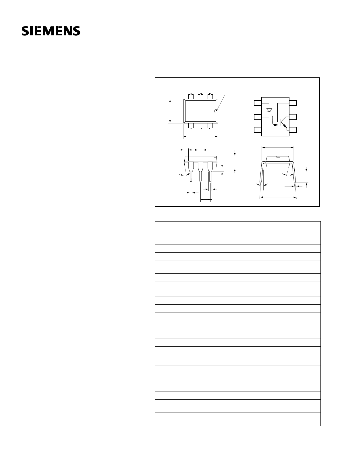
Dimensions in inches (mm)
pin one ID
3
.248 (6.30)
.256 (6.50)
4
.335 (8.50)
.343 (8.70)
.039
(1.00)
min.
4°
typ.
.018 (0.45)
.022 (0.55)
Electrical Characteristics
Parameter Symbol Min. Typ. Max. Unit Condition
Emitter
Forward Voltage V
Reverse Voltage V
Detector
Package
Saturated Current Transfer Ratio VCE=0.4 V
MCT5210
MCT5211
MCT5211
Current Transfer Ratio V
MCT5210
MCT5211
MCT5211
Ω
Collector-Base Current Transfer Ratio V
Ω
MCT5210
MCT5211
MCT5211
Saturation Voltage
MCT5210 V
MCT5211 V
(0–70°C)
12
5
.048 (1.22)
.052 (1.32)
6
Anode
Cathode
.130 (3.30)
.138 (3.50)
.031 (.080) min.
.031 (.80)
.035 (.90)
.100 (2.54) typ.
NC
3°–9°
1
2
3
.300 (7.62)
typ.
.010 (.25)
.300–.347
(7.62–8.81)
(25°C)
F
R
HFE 100 200 VCE=5 V
BV
CEO
BV
ECO
BV
CBO
I
CEO
CTR
CEsat
CTR
CEsat
CTR
CEsat
CTR
CTR
CTR
CTR
CB
CTR
CB
CTR
CB
CEsat
CEsat
1.2 1.5 V IF=5 mA
6VI
30 V IC=100 µA
7VI
70 V IE=10 µA
5 100 nA VCE=10 V
60
120
100
200
75
150
70
150
150
300
110
225
0.2
0.4
0.3
0.6
0.25
0.5
0.25 0.4 V IF=3.0 mA
0.25 0.4 V IF=1.6 mA
%
%
%
%
%
%
%
%
%
6
Base
5
Collector
4
Emitter
18°
typ.
.114 (2.90)
.130 (3.30)
=10 µA
R
I
=100 µA
C
=100 µA
E
IF=3.0 mA
I
=1.6 mA
F
I
=1.0 mA
F
=5.0 V
CE
=3.0 mA
I
F
I
=1.6 mA
F
I
=1.0 mA
F
=4.3 V
CE
IF=3.0 mA
I
=1.6 mA
F
I
=1.0 mA
F
I
=1.8 mA
C
IC=1.6 mA
1

Characteristics —
FORWARD VOLTAGE
SCU
continued
Parameter Symbol Min. Typ. Max. Unit Condition
°
Switching Characteristics (25
C)
Propagation Delay —High to Low
MCT5210
MCT5211
MCT5211
tPHL
tPHL
tPHL
10
20
40
s
µ
s
µ
s
R
R
R
=330
L
=750
L
=1.5
L
µ
Propagation Delay —Low to High
µ
MCT5210
MCT5211
MCT5211
tPLH
tPLH
tPLH
10
20
40
s
µ
s
µ
s
R
R
R
=330
L
=750
L
=1.5
L
IF=3.0 mA, VCC=5.0 V
Ω,
Ω,
IF=1.6 mA, VCC=5.0 V
Ω,
IF=1.0 mA, VCC=5.0 V
Ω,
IF=3.0 mA, VCC=5.0 V
IF=1.6 mA, VCC=5.0 V
Ω,
Ω,
IF=1.0 mA, VCC=5.0 V
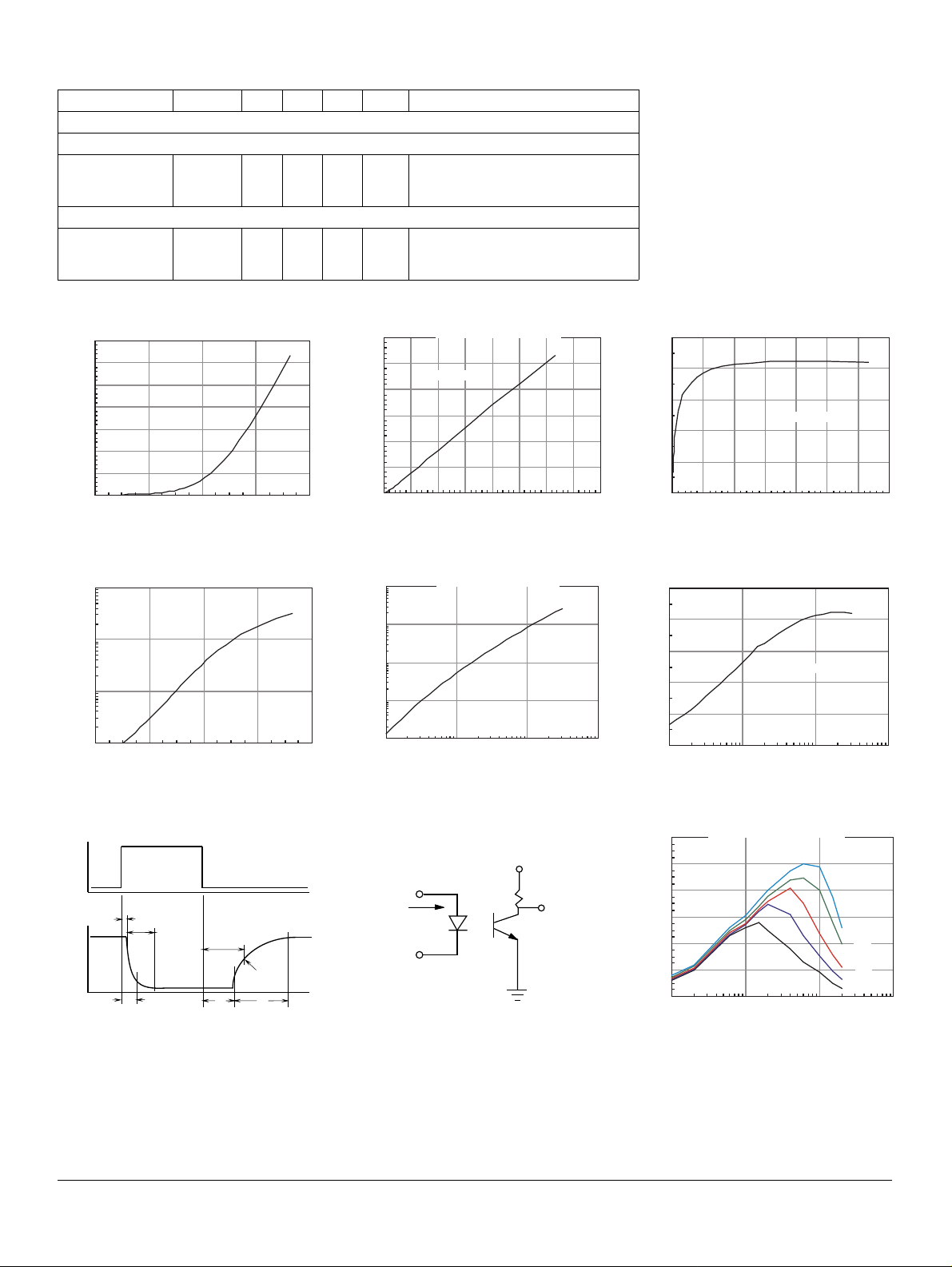
Figure 1. Forward current vs. forward
voltage
35
30
25
20
15
10
5
IF - LED Current - mA
0
Ta = 25°C
VF - LED Forward Voltage - V
Figure 2. LED forward current vs.
forward voltage
100
Ta = 25°C
10
1
IF - LED CURRENT - mA
.1
VF - LED FORWARD VOLTAGE - V
Figure 4. Collector base photocurrent
vs. LED current
300
250
200
150
100
50
Icb - PHOTOCURRENT - µA
1.41.31.21.11.0
1.41.31.21.11.0
0
Figure 5. Photocurrent vs. LED current
1000
100
10
1
Icb - PHOTOCURRENT - µA
.1
Ta = 25°C
IF - LED CURRENT - mA
Ta = 25°C
IF - LED CURRENT - mA
Figure 7. Collector base current transfer
ratio vs. LED current
1.0
0.8
0.6
0.4
0.2
4035302520151050
0.0
CTRcb - COLLECTOR BASE - CTR - %
IF - LED CURRENT - mA
TA = 25°C
Figure 8. Collector base current transfer
ratio vs. LED current
1.0
0.8
0.6
0.4
0.2
100101.1
0.0
CTRcb - COLLECTOR BASE - CTR - %
IF - LED CURRENT - mA
TA = 25°C
35302520151050
100101.1
Figure 3. Switching waveform
I
F
t
D
t
PHL
t
R
t
PLH
V
t
S
V
O
TH
=1.5 V
t
F
Figure 6. Switching schematic
V
= 5 V
CC
INPUT
R
L
2
V
OUT
Figure 9. Current transfer ratio
ratio vs. LED current
700
600
500
400
RATIO - %
300
200
100
IF - LED CURRENT - mA
MCT5210/5211
Ta = 25°C
Vce
10 V
5 V
2 V
1V
0.4 V
100101.1
 Loading...