

Page 1
C35(i), M35(i), S35i
Level 2.5e
Repair Documentation
V 1.0
V1.0 Page 1 of 35 ICM MP CC ST
P35 Company Confidential 03/01
Page 2

Table of Contents:
1 LIST OF LEVEL 2,5E PARTS P35............................................................................................................4
2 REQUIRED EQUIPMENT..........................................................................................................................5
3 REQUIRED SOFTWARE............................................................................................................................5
4 RADIO PART................................................................................................................................................6
4.1 POWER SUPPLY FOR RF PART.............................................................................................................6
4.2 FREQUENCY GENERATION...................................................................................................................7
4.2.1 DISCRETE 13MHZ VCXO................................................................................................................7
4.2.2 VCO LO1..............................................................................................................................................8
4.2.3 VCO LO2..............................................................................................................................................9
4.2.4 PLL IC LMX 2379............................................................................................................................10
4.3 ANTENNA SWITCH.................................................................................................................................11
4.4 RECEIVER.................................................................................................................................................12
4.4.1 LNA-PCN AND FILTER....................................................................................................................12
4.4.2 LNA-GSM AND FILTER...................................................................................................................13
4.4.3 MIXER, IF-AMPLIFIER AND DEMODULATOR .......................................................................14
4.4.4 BRIGHT IC BLOCKDIAGRAMM .................................................................................................15
4.5 TRANSMITTER........................................................................................................................................16
4.5.1 MOULATOR AND UP-CONVERSION LOOP................................................................................16
4.5.2 POWER AMPLIFIER AND ANTENNA SWITCH..........................................................................17
5 POWER SUPPLY........................................................................................................................................18
5.1 OVERVIEW AND VOLTAGES................................................................................................................18
5.2 POVER SUPPLY ASIC..............................................................................................................................19
5.3 BATTERY MEASUREMENTS AND CHARGING CONCEPT............................................................25
6 LOGIC PART...............................................................................................................................................29
V1.0 Page 2 of 35 ICM MP CC ST
P35 Company Confidential 03/01
Page 3

6.1 OVERVIEW LOGIC................................................................................................................................29
6.2 OVERVIEW EGOLD...............................................................................................................................30
6.3 OVERVIEW EGAIM...............................................................................................................................31
6.4 ACOUSTICS AND ILLUMINATION......................................................................................................32
6.4.1 GERNERAL.........................................................................................................................................32
6.4.2 RINGER AND VIBRA........................................................................................................................34
6.4.3 MICROPHONE AND LOUDSPEAKER...........................................................................................35
V1.0 Page 3 of 35 ICM MP CC ST
P35 Company Confidential 03/01
Page 4

1. List of available level 2,5e parts P35
ID-No Type Name(function)/Location Rep-Code Order No.
D100 IC GAIM /Logic 4GAI L36820-L6071-D670
D103 IC Egold/ Logic 4EGO L36810-G6096-D670
D200 IC ASIC/ Pow.Supply 4PSA L36145-J4682-Y16
D402 IC LMX-PLL/RF 4PLL L36820-L6038-D670
Z4450 IC Bright/RF 4BRI L36820-L6048-D670
N400/401 IC Volt. Reg./RF 4REG L36810-C6049-D670
N501 IC Op.Amp./RF 4OPA L36810-C6053-D670
N502 IC PA/RF 4PAM L36851-Z2002-A40
V211 Trans. Charg./Logic 4CHT L36830-C1046-D670
V305 Trans. Ringer-Light/logic 4RIT L36830-C1081-D670
V305 Trans. Vibra/logic 4VIT L36702-C1340-S67
V460 Trans. LNA/logic 4LNA L36840-C2039-D670
V501/502 Trans. TX/RF 4SWT L36840-C4013-D670
V508 Trans. TX/RF 4SWT L36840-C4014-D670
V306/800 Diode Vibra-Ringer/Logic 4RID L36840-D53-D670
Z100 Quartz Egold/Logic 4OSC L36145-F102-Y8 (B1 lay.)
4OSC L36145-F102-Y9 (B2 lay.)
Z601 Quartz 13MHz/RF 4VCX L36145-F220-Y4
Z404 VCO 1LO/RF 4VC1 L36145-G100-Y68
Z480 VCO TX/RF 4VCT L36145-G100-Y37
Z440 Filter IF/RF 4IFF L36145-K280-Y132
Z450 Filter RX-PCN/RF 4FI1 L36145-K280-Y133
Z451 Filter RX-PCN/RF 4Fi2 L36145-K280-Y135
Z460 Filter RX-GSM/RF 4FI3 L36145-K280-Y118
Z461 Filter RX-GSM/RF 4FI4 L36145-K280-Y121
V1.0 Page 4 of 35 ICM MP CC ST
P35 Company Confidential 03/01
Page 5

2. Required Equipment for Level 2,5e P35
Ø GSM-Tester (CMU200 or 4400S incl. Options)
Ø PC-incl. Monitor, Keyboard and Mouse
Ø Bootadapter 2000 (L36880-N9241-A200)
Ø Troubleshooting Frame P35 (F30032-A74-A1)
Ø Power Supply
Ø Spectrum Analyser (Advantest 3221)
Ø RF-Probe incl. Power Supply (e.g. from Agilent)
Ø Oscilloscope incl. Probe
Ø RF-Connector (N<>SMA(f))
Ø Power Supply Cables
Ø Dongle (F30032-P28-A1)
Ø BGA Soldering equipment
Reference: Equipment recommendation Level 2,5e
3. Required Software for Level 2,5e P35
Ø Windows NT Version4
Ø Winsui P35
Ø Winswup
Ø Windows software for GSM-Tester
Ø Software for 13MHz adjustment
V1.0 Page 5 of 35 ICM MP CC ST
P35 Company Confidential 03/01
Page 6

4. Radio Part
The radio part converts the I/Q base band signals supplied by the logic (EGAIM) Notes
into RF-signals with characteristics as per the GSM recommendation
(transmission) which are radiated by the antenna.
Or the radio part converts the received GMSK signal supplied by the antenna
into IQ base band signals which can then be further processed by the logic
(EGAIM). The radio part is designed for Dual Band operation and can therefore
serve the frequency bands EGSM900 and GSM1800. The radio part can never
transmit and receive in both bands simultaneously. However, the monitor time
slot can be selected independently of the frequency band.
Transmitter and receiver are of course never operated simultaneously.
The radio part consists of the following blocks:
• Power supply
• Synthesizer
• Receiver
• Transmitter
• Transmitter (Power amplifier)
• Antenna Switch
4.1 Power Supply RF-Part
Two voltage regulators (N400/401) with a nominal output voltage of 2.8V in the
SOT23-5 housing are used. The voltage regulator N400 is activated via
VCXOEN provided by the ASIC.
The voltage regulator N401 is activated via SLEEPQ provided by the Egold.
To reduce interference signals a 220µF electrolytic capacitor is
connected to the input of the regulators.
The name of the voltages are: a) UTXVCO activated by VCXOEN
and b) VCCBRIGHT activated by SLEEPQ
For both voltages BATT+ is required.
V1.0 Page 6 of 35 ICM MP CC ST
P35 Company Confidential 03/01
Page 7
4211
4.2 Frequency generation
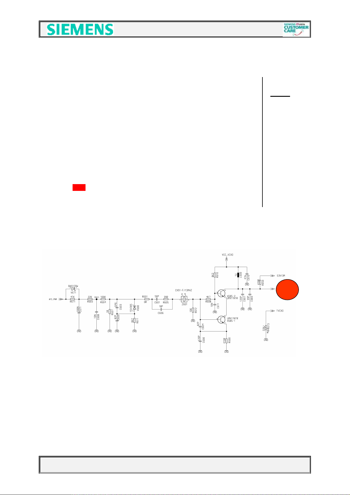
4.2.1 Synthesizer : The discrete VCXO (13MHz)
The generation of the 13MHz signal is done in the P35 via a discrete VCXO. Notes
A Colpitts oscillator with a post-switched buffer stage is used as oscillator switch.
The subsequent oscillating circuit (C607,C683, L600) and the resistor R650
create a de-coupling of the synthesiser from interference signals coming from the
logic.
The oscillator frequency is controlled by the (AFC_PNM) signal which is generated
from the EGOLD and the capacity diode V600.
To reduce the charging time of the low pass (R671, C671) the resistor R671 is
bridged by the diode V671
For the temperature control a temperature-dependent resistance R673 is placed
near the VCXO.
The required voltage VCC_VCXO is provided by the N400 (UTXVCO) through R411
The picture 4211 shows you the signal at the collector of the transistor V685.
V1.0 Page 7 of 35 ICM MP CC ST
P35 Company Confidential 03/01
Page 8
4221
4222
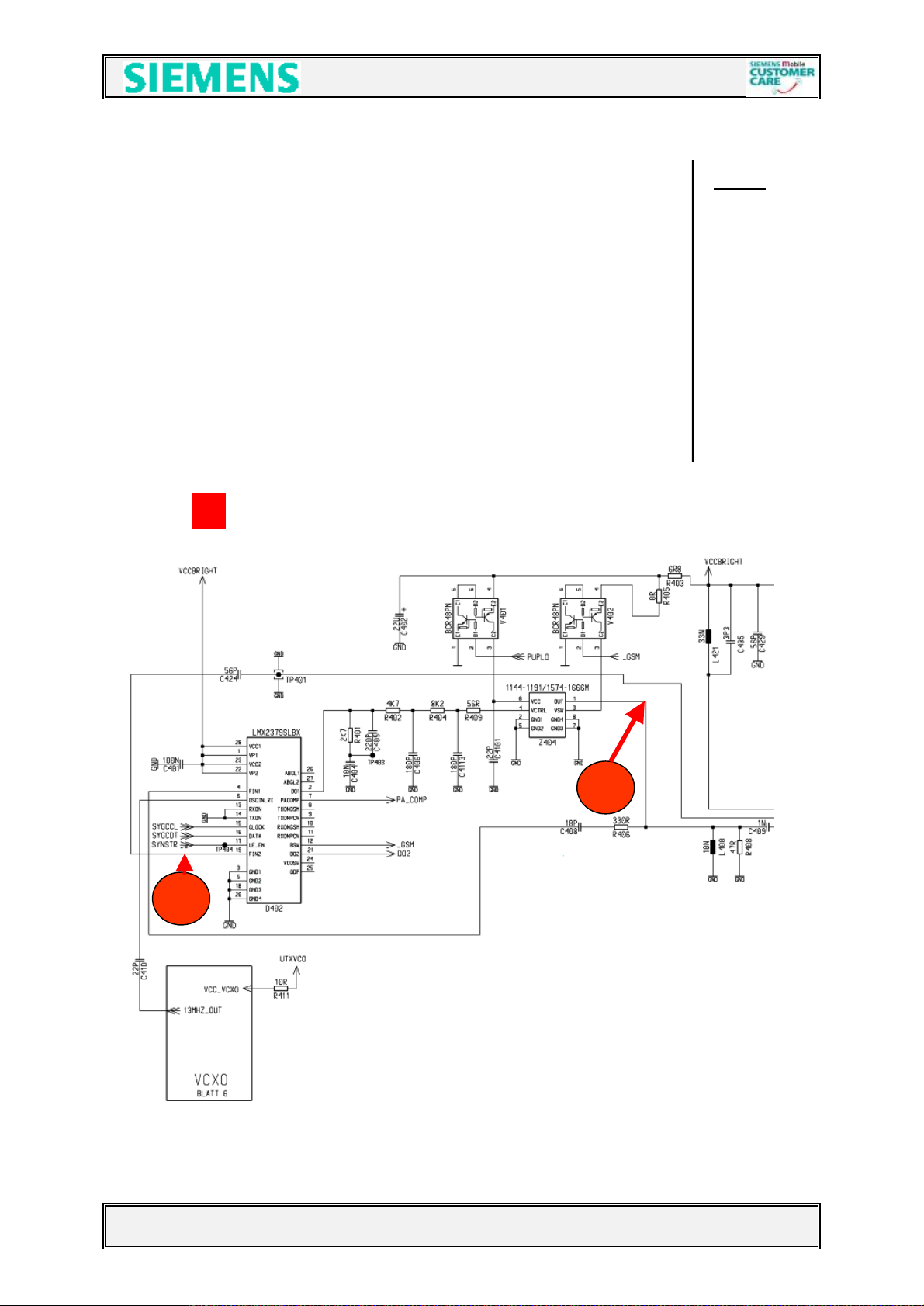
4.2.2 Synthesizer : LO1
The first local oscillator (LO1) consists of the PLL-IC (D402), a loop filter Notes
and a VCO (Z404) module. This LO1 circuit generates frequencies from
1144MHz to 1191MHz for GSM 900 operation and from 1574MHz to 1666MHz for
GSM 1800 operation. It is switched to select the channels in stages of 200kHz.
The loop filter has a limit frequency of approx. 10kHz and a periodic suppression.
The VCO module is switched on via the signal PUPLO (V401).
The switching between GSM900 and GSM1800 is done via the signal _GSM (V402),
generated by (D402) through the programming signals SYGCCL, SYGCDT,SYNSTR
The VCO output signal enables the BRIGHT IC to mix the IF-Frequency (225 MHz)
The VCO output is also guided to the PLL-IC (D402) to ensure the frequency stability
(DO1<>VCTRL). To do so the 13MHz frequency is used as the reference signal for
the PLL circuit.
The programming of the PLL-IC is realised by the EGOLD with the signals:
SYGCCL; SYGCDT and SYNSTR.
The required voltage VCCBRIGHT is provided by N401.
The _GSM (not GSM900) signal is on “H” level
The picture 4221 shows the VCO output signal
The picture 4222 shows the programming signals for the PLL
V1.0 Page 8 of 35 ICM MP CC ST
P35 Company Confidential 03/01
Page 9
4231
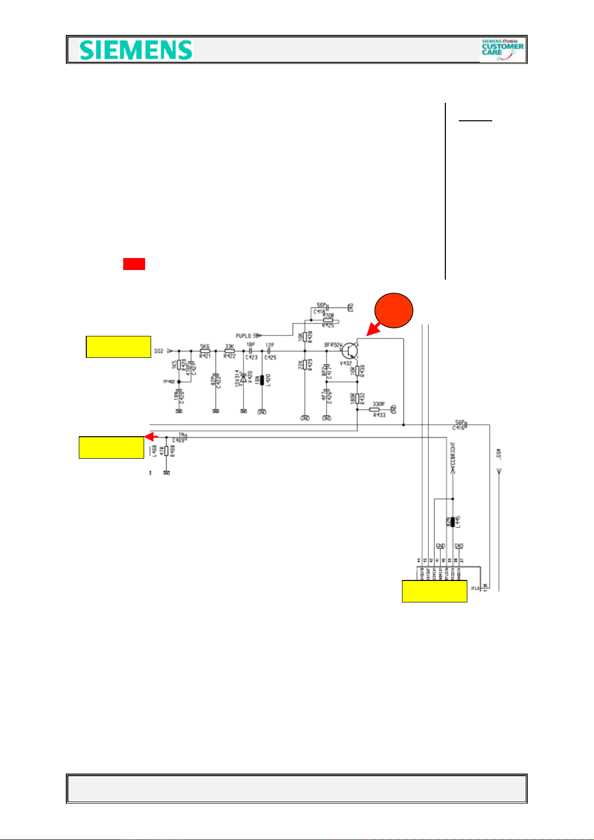
4.2.3 Synthesizer : LO2
The second local oscillator (LO2) consists of the PLL-IC (D402), a loop filter, the Notes
BRIGHT IC and a discrete VCO. The LO2 circuit generates the frequencies 520MHz
or 540MHz as required. The mobile phone normally uses the frequency 540MHz.
The LO2 switches to 520MHz in the GSM1800 TX mode only. The Signal (_GSM) is
used for switching. The loop filter has a limit frequency of approx. 10kHz and a
periodic suppression.
The oscillator is constructed discretely, whereby the active part and its operating
point setting are integrated in the BRIGHT (see BRIGHT Block diagram) .
The PUPLO signal is switching on the discrete LO2 circuit.
The BRIGHT IC is supplied via L445 with VCCBRIGHT
The required voltage VCCBRIGHT is provided by N401
The picture 4231 shows the LO2 output signal
from PLL
to PLL
Bright IC
V1.0 Page 9 of 35 ICM MP CC ST
P35 Company Confidential 03/01
Page 10
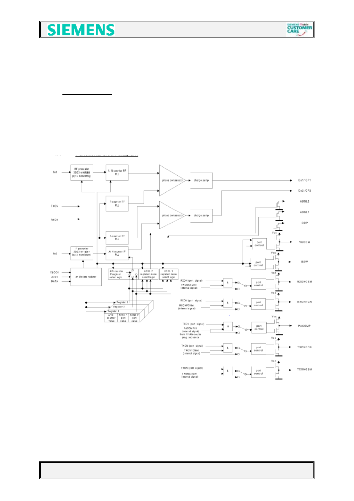
4.2.4 Synthesizer : PLL
PLL-IC LMX2379SLBX (D402)
Blockdiagramm
The required voltage VCCBRIGHT is provided by N401
V1.0 Page 10 of 35 ICM MP CC ST
P35 Company Confidential 03/01
Page 11
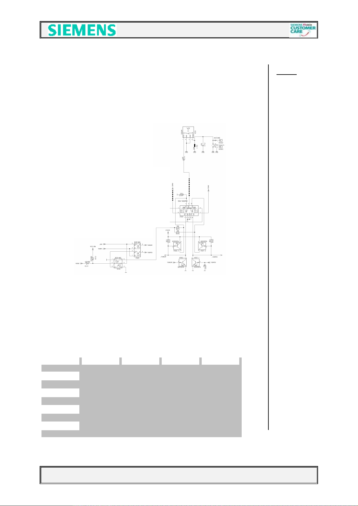
4.3 Antenna switch (mechanical/electrical)
Internal/External <> GSM900/1800 <> Receiver/Transmitter Notes
The P35 mobile consists of two antenna switches.
a: The mechanical antenna switch (connector X501) for the differentiation
between the internal and external antenna.
b: The electrical antenna switch (Diplexer Z503) for the differentiation between
the receiving and transmitting signals, just like the differentiation between
GSM900 and GSM1800
To do so the signals “_GSM; TXONPA; RXON2” are required to switch the
input signals VC1–VC4.
The matrix below shows the different conditions at the Diplexer and the
accompanying signals.
VC1 (pin2) VC2 (pin4) VC3 (pin8) VC4 (pin10)
GSM TX
GSM RX
PCN TX
PCN RX
high
low
low
low
low
high
low
low
low
low
low
high
low
low
high
low
V1.0 Page 11 of 35 ICM MP CC ST
P35 Company Confidential 03/01
Page 12

4412
4413
4414
from Antenna
Switch
4411
4.4 Receivers
4.4.1 Receiver: GSM1800-LNA and Filter
After the antenna switch, up to the first mixer the GSM1800 receiver circuit Notes
Consists of a ceramic front end filter (Z450),a LNA (Low Noise Amplifier V450) and
a ceramic inter-stage filter (Z451).
The front-end filter (double-pole ceramic filter) has an insertion loss of max. 1.5dB
with an intermediate frequency selection of minimum 32dB.
The GSM1800 LNA V450 is a discrete module with an amplification of approx. 17dB.
The collector current of the transistor is stabilised via an integrated regulating switch
inside the BRIGHT Z4450.The collector current is defined through the resistance of
the resistor R471. The LNA is switched on via the signal (RFIN2) from BRIGHT IC.
After the amplification an other inter-stage filter ((Z451) a 3-pole ceramic filter) is
used to reduce the amplification interference.
This filter has an insertion loss of maximum 3.7dB with an intermediate frequency
selection of minimum 38dB.
The non-symmetrical output of the filter (Z451) is connected to the 1st PCN mixer
via a balancing and adaptation circuit .(C454, L452, C459, C455) This circuit
converts the asymmetrical input signal into a symmetrical signal.
The required voltage VCCBright is provided by the N401
switch
to GAIM
IF-Circuit
V1.0 Page 12 of 35 ICM MP CC ST
P35 Company Confidential 03/01
Page 13

switch
4421
4422
4423
4424
Switch
4.4.2 Receiver: GSM900-LNA and Filter
After the antenna switch the GSM900 receiver signal runs through the SAW front Notes
end filter (Z460). The front end filter has an insertion loss of approx. 2.5dB and a
ripple of approx. 1dB.
The amplification of the subsequent LNA V460 has been reduced to approx. 18dB
The operating point stabilisation of the LNA transistor is accomplished via the
BRIGHT and the resistor R471. The LNA is switched on via the signal (RFIN1)
from BRIGHT IC. The output is adapted by corresponding components to the
subsequent SAW inter-stage filter (Z461). This filter has an insertion loss of approx.
3.5dB and a ripple of approx. 1.5dB. The symmetrical filter output of the inter-stage
filter is adapted to the input of the first mixer (Z4450).
The symmetrical output of the filter (Z461) is connected to the 1st GSM mixer
via an adaptation circuit .(C466, C467 L462)
The required voltage VCCBright is provided by the N401
to GAIM
IF-Circuit
V1.0 Page 13 of 35 ICM MP CC ST
P35 Company Confidential 03/01
Page 14

4432
4431
4433
4434
4.4.3 Receiver : Mixer, IF Amplifier and Demodulator
The BRIGHT IC (Z4450) has two separate input mixers one for EGSM900 and Notes
one for GSM1800. Both mixer blocks are designed as Gilbert cells and they are
switchable in the conversion gain (dynamic: 12dB for GSM and 10dB for PCN).
The mixing result for both mixers is an intermediate frequency from 225MHz.
For GSM900 the LO1 frequency is RX frequency plus intermediate frequency.
For GSM1800 the LO1 frequency is RX frequency minus intermediate frequency.
After passing an external IF Filter (Z440) the signal is mixed down with the LO2 to
45MHz. After further filtration the 45MHz IF signal arrives at the programmable IF
amplifier in the (Z4450). This amplifier has a dynamic of 96dB and can be set via a
6-bit programming word (PGCSTR;SYGCDT;SYGCCL) in 2dB steps.
Finally the signal is mixed down in the demodulator to DC in order to generate the
differential I and Q signals.(RX_I,RX_IX-RX_Q,RX_QX) This signals are guided to
the EGAIM to the A/D converters in the base band path.
2 LO
from LNA
IF-Circuit
to GAIM
V1.0 Page 14 of 35 ICM MP CC ST
P35 Company Confidential 03/01
Page 15

4.4.4 Bright IC
V1.0 Page 15 of 35 ICM MP CC ST
P35 Company Confidential 03/01
Page 16

4512
4511
PCN:540/520 MHz
135 MHz
4.5 Transmitter
4.5.1 Transmitter: Modulator and Up-conversion Loop
The P35 modulation is based on the principle of the up-conversion modulation Notes
phase locked loop and is accomplished via the BRIGHT IC(Z4450).
The BRIGHT IC provides the quadratic modulator with the TX IF signals
(GSM 270MHz/ PCN 135/130MHz). Whereby these frequencies are mixed from
the second local oscillator signals.
This “wrong GMSK RF signal” is compared in a phase detector with the down mixed
“final GMSK RF signal”.
To get the comparison signal the TXVCO signal is mixed with LO1 signal.
With the help of the 1.LO the GMSK-RF signal appearing at
the output of the TXVCO (Z480) is mixed to a ZF (GSM 270MHz/ PCN 135/130MHz)
below the TX signal and is led on to the phase detector. The I-Q modulated signal in
the ZF position (GSM 270MHz/ PCN 135/130MHz) is also led to the phase detector.
The output signal of the phase detector passes a discrete loop filter formed from
capacitors and resistors and controls the TXVCO to work on the right frequency.
This large loop band width guarantees that the regulating process is considerably
quicker than the changes in the modulation signal.
The TXVCO is a so-called two-in-one VCO, this means the VCO module contains
the GSM-VCO and the PCN-VCO in one housing.
Via a transistor switch (V480) by using the signal _GSM the TXVCO is switched
from GSM to PCN.
The required voltage VCCBright is provided by N401
The required voltage UTXVCO is provided by N400
1.LO
1150-1185 MHz
1580-1655 MHz
880-915 MHz
1710-1785 MHz
TX-VCO
2.LO
GSM:540 MHz
270 MHz
130/135 MHz
Phase
Detector
TP
260 MHz
270 MHz
130 MHz
90°
: 2
I Q
Mod ulator
Mod Signal
270 MHz
130/135 MHz
V1.0 Page 16 of 35 ICM MP CC ST
P35 Company Confidential 03/01
Page 17

4522
4521
4523
4524
4.5.2 Transmitter : Power Amplifer Amplifier and Antenna Switch
Splited by a discrete circuit into GSM900 GSM1800 the TXVCO output signal Notes
arrives at the power amplifier. The dual band power amplifier module (N502)
is assembled on a ceramic substrate in one housing. The module amplifies the
output signal of the TXVCO to the required PCL (controlled by the feedback circuit
according to settings from the logic) .The different amplifiers are switched on by the
TXONPCN/TXONGSM via the transistor (V508). The signal PA_Comp is required for
the operation point setting of low GSM PCLs. The power amplifier is feeded directly
from the battery (BATT+).
After amplification the signal passes on the way to the antenna the diplexer (Z503)
and antenna connector (X501)
A part of the TX output signal is decoupled via a directional coupler (realised by
conductive tracks) and is equalised at a detector diode (V505).
This so gained voltage is compared by an operation amplifier (N501) with the
PA_RAMP signal provided by the GAIM, to ensure that the PA is working within the
required PCL´s
For temperature compensation the other part of the detector diode (V505) is used.
The required voltage BATT+ is provided by the battery.
The required voltage VCC2,8SW is provided by transistor V481.
V1.0 Page 17 of 35 ICM MP CC ST
P35 Company Confidential 03/01
Page 18

5. Power Supply
5.1 Overview and Voltages
Notes
The following restrictions must be observed:
• The phone cannot be operated without battery.
• The phone will be damaged if the battery is inserted the wrong way round
(the mechanics of the phone prevent the battery from being put in the
wrong way round. The electric system assumes that the battery as been
inserted correctly.
V1.0 Page 18 of 35 ICM MP CC ST
P35 Company Confidential 03/01
Page 19

5.2 STV-ASIC
The power supply ASIC contains the following functions: Notes
• Control of “switching on” the mobile phone via
1.The ON/OFF Key. (ON_OFF)
2.The bottom connector with (External Power)
3.The Real Time Clock RTC (ON_OFF2)
• Watchdog monitor
1.Control of “switching off” the mobile phone via WATCHDOG_µP.
2. Watchdog observation
• Switch off of mobile phone in the case of overvoltage at battery connection.
• Generation of RESET signal for E-GOLD, E-GAIM, Flash and MMI components
• Generation of 2.90 V via linear controller for the logic IC.
• Generation of 2.65 V via linear controller for the logic IC.
• Generation of 2.20 V via linear controller for the logic IC.
• Battery charge support:
• Low battery detector
A low voltage comparator in the ASIC will monitor the battery voltage. If the
voltage drops below 3.05 V ± 60mV, then a high signal will be created at output
LOW_BATTERY.
If the phone has not been used for a longish time (longer than approx. 1 month),
the battery could be totally self-discharged (battery voltage too low), so that it is not
possible to charge the battery via the normal charging circuit.
Only trickle charging is possible below a level of 3.2 V (charging current <10mA).
After approx. 2 hours of trickle charging it is possible to charge the phone via the
“normal” charging circuit.
All internal timers and pulses are derived from a 900 kHz ± 10% internal oscillator.
Responsible for the frequency stability is an external resistor (R228) (1%) at the
RREF pin
V1.0 Page 19 of 35 ICM MP CC ST
P35 Company Confidential 03/01
Page 20

Pin Configuration in accordance with Component Specifications:
Functions
“Switching on” the
mobile phone
Pin
Requirements
ON_OFF
EXT_POWER
ON_OFF2
Implementation / Explanation
The following 3 “switch on” conditions will be accepted:
• Falling slope to ON_OFF
• Rising slope to EXT_POWER
• Rising slope to ON_OFF2
If one of this 3 conditions is recognised, then the ASIC
switches into the POWER-Up state and the internal oscillator
starts.
After T1 (approx. 60ms) the source of the “switch on” signal is
checked again. If the required level is no longer present, then
the mobile phone will not switch on and the ASIC switches to
the POWER-DOWN mode. If the required level is still there,
the mobile phone will “switch on”. To do so VCXOEN (internal
SLEEP) will go to HIGH and the 3 voltage regulators VREG1
(2,9V), VREG2 (2,0V)and VREG3 (2,65V) will switch on.
After T2 (approx. 60ms) counted from switch on (i.e. 120ms
from initial recognition of the switch on condition) the supply
voltages for 1V92, 2V65 and 2V9 will be checked. If the 1V92
and 2V9 voltages are in order, then timer T3 will start and will
enable the RESET after approx. 60ms.
To ascertain by what signal the phone was switched on. The
E-Gold checks the following signals.
KB7 >>>>>>>>>>> to check the “On-Off Keypad button”
RTC_INT>>>>>>>> to check the timer “on-off”
EXT_Power_µc>>> to check ON-OFF via accessory
V1.0 Page 20 of 35 ICM MP CC ST
P35 Company Confidential 03/01
Page 21

Functions
Watchdog
monitoring
Regular switch
off of the mobile
phone
Low Voltage
Detector
Reset Signal
Switch off of the
phone in the
case of
overvoltage at
the battery
Voltage Supply
for the Logic
Pin
Requirements
WATCHDOG_UP
Implementation / Explanation
The first Watchdog Impulse of the E-GOLD
• must be operated at the latest 800ms after the
rising edge of the “Reset” signal and
• the WD-Signal must have a rising edge.
If one of these conditions is not fulfilled, the mobile phone will
switch off.
If this conditions are fulfilled, rising and falling edges are
evaluated alternately to reset the WD-Timer. With each edge
at the WATCHDOG_UP pin WD-Timer will be reseted. The
next (inverted to the previous one) edge must have to
occur within a time of 0.4s...2.6s. If the next slope is
recognised before expiry of 0.4s or after an expiry of 2.6s or if
the next recognised edge is not inverted, then the mobile
phone will switch off.
WATCHDOG_UP
Switching off of the phone is possible, as described in the
watchdog monitoring control, if the E-GOLD is not longer
serving the WATCHDOG_UP pin.
Switching off of the phone means:
RESET to LOW
POWER_ON to LOW
CHARGE to HIGH-Z.
Regulator 1V92, 2V65 and 2V9 OFF
The ASIC goes into the POWER-DOWN mode.
LOWVDD
If the measured battery voltage is below the limit of 3.05V ±60
mV, then a HIGH signal will be generated at the LOWVDD
output pin. This signal causes an interrupt at the E-GOLD.
RESET
Power-Up:
During the entire switch on procedure the RESET signal is on
“LOW-Level”. If the switch on conditions are fulfilled the
change to “HIGH-Level” is taken place after 180ms.
Power Fail:
In the “unit on“ mode the voltage levels of the 1.92V and 2.9V
voltage supply shall be monitored. If one of this voltages drops
below a certain level for longer than 10µs, the RESET signal
switches to “LOW-Level”.
VDD In the case of a too high voltage at the VDD,(voltage level
5.8V ± 0.2V within 1µs), the mobile phone will switch off.
VREG2
U2V0
The linear controller is designed for 1.92V(±3%) and a
maximum current of 140 mA.
It consists basically of an internal operation amplifier, an
integrated p-channel output transistor as well as an external
capacitor (C = 2.2µF) for stabilising the voltage. This regulated
voltage is measured internally.
In case of an internally measured voltage >3.1V , the output
transistor will switch off.
V1.0 Page 21 of 35 ICM MP CC ST
P35 Company Confidential 03/01
Page 22

oltage >3.1V , the output
In case of an internally measured voltage >3.3V , the output
Voltage Supply
for the Logic
Voltage Supply
for the Logic
VREG3
U2V65
VREG1
U2V9
The linear controller is designed for 2.65V(±3%) and a
maximum current of 100 mA.
It consists basically of an internal operation amplifier, an
integrated p-channel output transistor as well as an external
capacitor (C = 2.2µF) for stabilising the voltage. This regulated
voltage is measured internally.
In case of an internally measured v
transistor will switch off.
The linear controller is designed for 1.92V(±3%) and a
maximum current of 140 mA.
It consists basically of an internal operation amplifier, an
integrated p-channel output transistor as well as an external
capacitor (C = 2.2µF) for stabilising the voltage. This regulated
voltage is measured internally.
Voltage Supply
for
SIM-CARD
Charge Support
CCVZQ
CCVCC
CHARGE,
CHARGE_uP,
TBAT
transistor will switch off.
The voltage supply for the SIM-CARD (CCVCC) is switched
by the signal CCVZQ from the E-GOLD via a “LOW” at pin 12
The output signal CCVCC can be measured at pin 13 (3V)
The picture 5212 shows the CCVCC depending on the signal
5211 CCVCZQ from EGOLD
For controlling the battery charge function, a charge support is
integrated in the ASIC. It consists basically of an internal
current source, a temperature sensor, an external charge FET
with a Pull-Up resistor between the source and the gate of the
charge FET.
The current source is switched on trough a rising edge of the
CHARGE_UP signal and generates an “LOW” at pin 3
(Charge). With this “LOW” the charge FET becomes
conducting.
Exceptions:
a) The temperature comparator does give a signal for high
temperature
b) An overvoltage is present at the VDD.
C) A falling edge at the CHARGE_UP.
V1.0 Page 22 of 35 ICM MP CC ST
P35 Company Confidential 03/01
Page 23

AVDDDVDDDVSSAVSS
RREF
WATCHDOG_uC
ON/OFF1
ON/OFF2
EXT_POWER
SLEEPQ
VDD_LDO
3
Control Unit
1.92 V 140 mA
Linear Regulator
2,9 V 140 mA
Linear Regulator
2,65 V 100 mA
Linear Regulator
RESET_2V0
RESET_2V65
POWER_ON
LOW_BATT
VLDO2V0
VLDO2V9
VLDO2V65
VDD_LDO_RTC
TBAT
CHARGE_uC
VSIM_IN
VSIM_ON
< 55°C ?
2.0 V 1 mA
Low Power
Regulator
&
Charge FET Driver
SIM Supply Switch
VLDO_RTC
CHARGE
VSIM_OUT
V1.0 Page 23 of 35 ICM MP CC ST
P35 Company Confidential 03/01
Page 24

Example of a timing diagram (switch on by the keypad)
Example of a timing diagram (Watchdog Observation)
1. WD-Observation
2. WD-Observation
3. WD-Observation
V1.0 Page 24 of 35 ICM MP CC ST
P35 Company Confidential 03/01
Page 25

5211
5212
Battery
A NiMH battery with a nominal capacity of 500mAh is used for C35(i) and M35(i) Notes.
A temperature sensor (NTC 103HAT) is integrated to monitor the charge.
For S35(i) a LiIon battery is used with a nominal capacity of 600mAh
Charging Concept
General
The battery is charged in the unit itself. The hardware and software is designed for
both for NiMH batteries and for Li-Ion batteries.
As soon as the phone is connected to an external charger, charging starts.
(The customer can see this via the “Charge” symbol in the display).
During normal use the phone is being charged (restrictions: see below).
Charging is enabled via an MOS-FET switch. This MOS-FET switch activates the
circuit for the external charger to the battery. The processor takes over the steering
of this switch depending on the charge level of the battery, whereby a disable
function in the STV-ASIC hardware can interrupt the charging in the case
of too high temperature of the battery, or an overvoltage at VDDLP(D200).
A line (SB) is used for recognition and control of the S25 charger.
The P35 external power supply is equiped with a high Ohm input and will therefore
be recognised as a rapid charger. The charging software is able to charge the
battery within a range from 400-700mA.
If the MOS-FET is switched off, only trickle charging is active.
For controlling the charging process it is necessary to measure the battery cell
temperature (only NiMH), the ambient (phone) temperature and the battery voltage.
The temperature sensor is a NTC resistor with a nominal resistance of 10kΩ at 25°C.
The determination of the temperature is achieved via a voltage measurement on a
voltage divider consisting of the NTC and 2 other resistors(D100). The NTC
for measuring the battery cell temperature is assembled in the battery pack. The
NTC for the ambient temperature is soldered on the PCB(R673).
V1.0 Page 25 of 35 ICM MP CC ST
P35 Company Confidential 03/01
Page 26

Measurement of Battery and Ambient Temperature Notes
The voltage equivalent of the temperature on the voltage divider is measured
as the difference against a reference voltage of the EGAIM. For this, the
integrated Σ∆ converter of the EGAIM of the RX-I base band branch is used.
Via an analog multiplexer, either the RX-I base band signal,(the battery temperature
Voltage) or the ambient temperature voltage can be switched to the input of the
converter. The 1-Bit current of the converter will be subjected to a data reduction via
the DSP circuit so that the measured voltage (for battery and ambient temperature)
will be available at the end as a 10-bit data word.
Measurement of the Battery Voltage
Analog to the I-branch either the RX-Q base band signal or the battery voltage can
be measured in the Q-branch. The processing in the DSP circuit is done similar to
the I-branch. The GAIM is specified for voltages measurement s at the input pin G2
(VBAT) from 3V...5.5V.
Timing of the Battery Voltage Measurement
Unless the battery is going to be charged, the measurements are made in the
TX time slot. While charging the measurement is done after the TX time slot.
At the same time, either the battery temperature (in the I-branch) and the
battery voltage (in the Q-branch) or the ambient temperature in the I-branch can be
measured
Other combinations are not possible. For the time of the measurement
the multiplexer in the EGAIM must be programmed (EGOLD) to the corresponding
measurement.
V1.0 Page 26 of 35 ICM MP CC ST
P35 Company Confidential 03/01
Page 27

Recognition of the Battery Type
The integrated NTC in the battery pack is used as a coding element for the Notes
NiMH battery pack.
If no resistance is recognised, then the battery is charged via the Li-lon charging
process.
Charging Characteristic of Lithium-Ion Cells
Li-Ion batteries are charged with a U/I characteristic, i.e. the charging current is
regulated in relation to the battery voltage until a minimal charging current has been
achieved. The maximum charging current is approx. 700mA, the minimum current
is around 100mA. The battery voltage may not go above 4.2V ±50mV. The allowed
starting temperature for charging the phone is within the range from 5...40°C,
and the allowed temperature while charging is taking place is from 0...45°C.
Outside this temperature range the battery will not be charged.
Trickle Charging
A special circuit permits charging the battery if the normal charging circuit is not
working due to a low level of battery voltage.
This charging current will be about 10mA max. This trickle charging circuit is
voltage-restricted, so that a battery can not be overcharged under no circumstances.
Trickle charging is a way to charge completely discharged batteries up to a voltage
which allows the logic to switch to normal charging automatically.
V1.0 Page 27 of 35 ICM MP CC ST
P35 Company Confidential 03/01
Page 28

Restrictions:
• A battery which is completely discharged can not be charged quickly (normal). Notes
In this case the battery is charged via a trickle charging with approx. 10mA.
However, the charging symbol is not shown in the display due to the not working
logic.
The charging time for the trickle charging (until the battery can be recharged
quickly) is approx. 4 hours. If, within this time, a voltage of 3.2V is exceeded,
the ASIC switches into the Charge-Only Mode.
In some circumstances it can happen that, after switching on, the voltage
collapses so strongly that the mobile phone switches off again. In this case
trickle charging continues until the user breaks off the trickle charging in order to
activate the rapid charge and starts recharging again (e.g. by pulling out the plug
from the mains supply and plugging in again!).
• A phone with a fully charged Li-Ion battery cannot be charged in the standby
or talk modus in the beginning, because any input current would cause an
increase off the battery voltage above the maximum permissible value. If, through
using the phone, the battery has been discharged down to 95%
the battery can be charged again.
• The phone cannot be operated without a battery.
• The phone would be destroyed if the battery were wrongly poled:
⇒ This is prevented mechanically by the design.
⇒ electrically, a correctly poled battery is presumed, i.e. correct poling must be
guaranteed by suitable QA measures at the supplier. If an unsuitable
charger is connected, the mobile phone can be destroyed:
⇒ a charger voltage >15V can destroy resistors or capacitors in the current
supply path.
⇒ a charger voltage >20V can destroy the MOS-FET switch transistor in the
current supply.
V1.0 Page 28 of 35 ICM MP CC ST
P35 Company Confidential 03/01
Page 29

6. Logic Part
6.1 Overview Logic
V1.0 Page 29 of 35 ICM MP CC ST
P35 Company Confidential 03/01
Page 30

6.2 Overview EGOLD
TMS
TCK
TDO
VBIN
VBOUT
VCLK
BPDM2
BPDM1
DACI
DACQ
TDI
TRST
2 MHz (to GAIM)
PE.1
RXD1 / EX1IN & T5EUD /
TXD1 / CC04IO / PE.0
DSPOUT0 / A22 / PF.3
Interface
DSP Serial
Communication
Enhanced Handsfree / DAI
5
Unit
Cipher
A51/52
Audio & Speech
HW
Viterbi
H. Meschede, HL AS CR CE,
16 bit I/O Ports
E-GOLD Architecture
Enable Signals to
X- and PD-Bus
VCXO_EN / - / PE.8
VSSa
VDDa
PDOUT / A23 / PF.4
CLKSXM / A21 / PF.5
CLKANA
F13M
RXDD / RXD1 / PF.7
RFSD / - / PF.9
523
SCLK / T6EUD / PF.8
TFSD / T2IN / PF.10
TXDD / TXD1 / PF.6
RXD0 / - / PE.3
TXD0 / - / PE.4
SSCCLK / - / PE.5
MTSR / - / PE.6
MRST / - / PE.7
RTCOUT
VDDRTC
F32K
requires ext. crystal
and special bondout
Peripherals
Peripheral Enable
Clock Generation
2
ASC0
SPI
SSC
compatible
RTC
Osc.
32.768 kHz
RESET_IN
DSP Timer2
Accelerator
DSP Timer1DSP Timer1
Power
Generator
Management
ASC1
Watchdog
GPT1/GPT2
Detect
Autobaud
32 kHz
2 x 8 bit
CAPCOM
16
8
CC00IO / T3OUT / PC.2
READY / WAKEUP / PC.1
CC01IO / NMI & DSPOUT2 / PE.2
CC02IO / - / HOLD & DSPOUT1 / PF.0
RX and TX
Voiceband Filters
P RAM
Y RAM
5k x 16
P ROM
48k x 16
2k x 16
Speech Coding (FR, HR, EFR)
OAK+ DSP
ž Interleaving / De-Interleaving
ž Speech Decoding (FR, HR, EFR)
ž
52 MHz
Baseband Filter
X RAM
6k x 16
X ROM
18k x 16
De-Interleaving 12k x 4
16 bit write access
4/16 bit read access
Channel Coding (FR, HR, EFR)
ž Level Measurement
Voice Memo / Voice Dialing
ž Channel Decoding (FR, HR, EFR)
ž
ž Equalization
ž Encryption / Decryption
ž
GMSK Modulator
Interleaving
2 x 28 x 116 x 1
Dual Port 512 x 16
Shared Memory
Bus
Unit
Interrupt Controller
Interface
SEIB
OCEM
X-Bus
Block
Boot
1k x 16
PRAM
MCU
C166CBC
OCDS DPEC
13 MHz / 32 kHz
READY#
NMI#
HOLD#
HLDA#
CLKOUT
RSTOUT#
60
Interrupt
Extension
PD-Bus
6
Multicore
ID Register
CLKOUT / CC05IO / PC.0
T5IN / T2EUD & T3IN / PC.4
CC06IO / A21 & EX7IN / PF.11
HLDA / CC03IO & DSPIN0 & T2IN / PC.3
Debug Support
MON1
MON2
TRIGIN
TRIGOUT
DSPOUT1 / A22 / PF.1
1k x 16
Dual Port RAM
Interrupt Controller
External
8 16
8
D(7:0)
A(20:0)
D10 / - / PA.10
D11 / - / PA.11
D13 / T7IN / PA.13
D8 / CC20IO / PA.8
D9 / CC16IO / PA.9
D12 / EX5IN / PA.12
D14 / CC22IO / PA.14
D15 / CC18IO / PA.15
1k x 16
PROM
Controller
Bus & Port
21 24
RD
BHE / CC00IO / PF.15
AFC Unit
CS(4:0)2
5
3
WR
CS0
CS1
AFC
CS2 / CC02IO / PF.12
CS4 / DSPOUT2 / PF.14
RSTOUT / EX6IN & T3EUD / PF.2
CS3 / EX4IN & DSPIN0 & T4EUD / PF.13
JTAG
TAP Controller
Boundary Scan
Company confidential
4
RF Control
GSM
TDMA Timer
SRAM
xk x 16 (x = 0...64)
High Speed
Interface
SIM card
Keypad
Pulse-Carry Mod.
Interface
3 3
5
9
to MCU &
Clock Generation Unit
(F=512, D=8/16)
64
VSS2.0x, x=a,b,c
VSS2.(4:1)
I/O Driver
VDD2.0x, x=a,b,c
VDD2.(4:1)
VSS1.(2:0)
Core
VDD1.(2:0)
RFCLK
RFDATA
RFSTR0
RFSTR1
RFSTR2 / CC07IO / PD.0
RFSTR3 / CC18IO / PD.1
RFSTR4 / EX2IN / PD.2
GAIMCLK
GAIMSTR
GAIMDATA
GAIMRXON
T_OUT0
T_OUT1
T_OUT2
T_OUT3
T_OUT4 / DSPIN0 / PD.3
T_OUT5 / CC17IO / PD.4
T_OUT6 / T4IN / PD.5
T_OUT7/ CAPIN / PD.6
T_OUT8 / CC23IO / PD.7
T_OUT9 / T7IN & EX3IN / PD.8
T_OUT10 / EX1IN & DSPIN1 / PD.9
T_OUT11 / CC19IO / PD.10
T_OUT12 / A23 / PD.11
CCIN
CCIO
CCVZ / - / PB.10
CCLK
CCRST
& T6IN / PB.11
CCIOSW / T6OUT & T0IN
KP0 / T2EUD & EX0IN / PB.0
KP1 / CC06IO / PB.1
KP2 / CC20IO / PB.2
KP3 / CC16IO / PB.3
KP4 / - / PB.4
KP5 / - / PB.5
KP6 / EX5IN / PB.6
KP7 / T7IN / PB.7
KP8 / CC22IO / PB.8
KP9 / CC18IO / PB.9
V1.0 Page 30 of 35 ICM MP CC ST
P35 Company Confidential 03/01
Page 31

6.3 Overview EGAIM
V1.0 Page 31 of 35 ICM MP CC ST
P35 Company Confidential 03/01
Page 32

6.4 Acoustics and Illumination
6.4.1 General Notes
The Electro-Acoustic components are: a) Loudspeaker
b) Microphone
c) Ringer
d) Vibra
The Acoustic components are driven and controlled from the EGOLD (Ringer,Vibra)
via the signals Ringer_µC and Vibra_µC
and from the EGAIM (Earpiece, Microphone) via the signals
EPP_HK, EPN_HK for the (Earpiece) and MICP,GND_MICRO for the (Microphone).
V1.0 Page 32 of 35 ICM MP CC ST
P35 Company Confidential 03/01
Page 33

The Illumination: a) Display
b) Keypad
Notes
V1.0 Page 33 of 35 ICM MP CC ST
P35 Company Confidential 03/01
Page 34

6.4.2 Ringer and Vibra
The vibrator is activated by the transistor V307 via the Signal Vibra_µC from Notes
Egold. Batt+ is required to provide the VIBRA. The diode V306 is used to protect
the circuit against over voltage and switching spikes.
The ringer is connected to Batt+. The ringing tone is generated by a pulsing signal
Ringer_µC from the EGold which is switching the FET V305-2 at the wanted
frequency
V1.0 Page 34 of 35 ICM MP CC ST
P35 Company Confidential 03/01
Page 35

6.4.3 Microphone and Loudspeaker
Notes
V1.0 Page 35 of 35 ICM MP CC ST
P35 Company Confidential 03/01
 Loading...