Siemens A36, A40, A35 Service Manual
A35/A36/A40
Level 2.5e
Repair Documentation
V 1.0
V1.0 Page 1 of 38 ICM MP CC ST
A35-A36-A40 Company Confidential 09/01

Table of Contents:
1 LIST OF LEVEL 2,5E PARTS A35/36......................................................................................................4
2 REQUIRED EQUIPMENT..........................................................................................................................5
3 REQUIRED SOFTWARE............................................................................................................................5
4 RADIO PART................................................................................................................................................6
4.1 POWER SUPPLY FOR RF PART.............................................................................................................6
4.2 FREQUENCY GENERATION...................................................................................................................7
4.2.1 DISCRETE 13MHZ VCXO................................................................................................................7
4.2.2 VCO LO1..............................................................................................................................................8
4.2.3 VCO LO2..............................................................................................................................................9
4.2.4 PLL IC PART OF SMARTI............................................................................................................10
4.3 ANTENNA SWITCH.................................................................................................................................11
4.4 RECEIVER.................................................................................................................................................12
4.4.1 RECEIVER GSM 900/1800................................................................................................................12
4.4.2 MIXER, IF-AMPLIFIER AND DEMODULATOR .......................................................................13
4.4.3 SMARTI IC ........................................................................................................................................14
4.5 TRANSMITTER........................................................................................................................................15
4.5.1 MOULATOR AND UP-CONVERSION LOOP................................................................................15
4.5.2 POWER AMPLIFIER AND ANTENNA SWITCH..........................................................................16
5 POWER SUPPLY........................................................................................................................................17
5.1 OVERVIEW AND VOLTAGES................................................................................................................17
5.2 POVER SUPPLY ASIC..............................................................................................................................18
6 BATTERY AND CHARGING....................................................................................................................24
6.1 BATTERY...................................................................................................................................................24
6.2 CHARGING CONCEPT............................................................................................................................24
V1.0 Page 2 of 38 ICM MP CC ST
A35-A36-A40 Company Confidential 09/01

7 LOGIC PART...............................................................................................................................................26
7.1 OVERVIEW LOGIC................................................................................................................................26
7.2 OVERVIEW EGOLD+............................................................................................................................28
7.3 OVERVIEW EGAIM INSIDE EGOLD+..............................................................................................29
8 MMI FUNCTIONS......................................................................................................................................32
8.1 ACOUSTICS................................................................................................................................................32
8.1.1 VIBRA...................................................................................................................................................32
8.1.2 MICROPHONE AND LOUDSPEAKER (RINGER).......................................................................33
8.2 LIGHT (KEYPAD AND BACKLIGHT)..................................................................................................35
8.3 SIM-CARD AND DISPLAY......................................................................................................................36
8.4 CONNECTORS...........................................................................................................................................37
8.4.1 I/O CONNECTOR...............................................................................................................................37
8.4.2 BATTERY CONNECTOR..................................................................................................................38
V1.0 Page 3 of 38 ICM MP CC ST
A35-A36-A40 Company Confidential 09/01

1. List of available level 2,5e parts A3x
ID-No Type Name(function)/Location Rep-Code Order No.
V100 Transistor TXon1/Logic 4SWT L36840-C4009-D670
D100 IC Egold+/Logic 4EGO L36810-G6103-D670
Z100 Quartz OSC_Egold+/Logic 4OSC L36145-F102-Y10
V200 Transistor Charge/Logic 4CHT L36830-C1064-D670
D200 IC ASIC/Pow.Supply 4SPA L36145-J4682-Y23
N201 IC Volt.Reg./Logic 4REG L36810-C6062-D670
V193 Transistor Light/Logic 4LIT L36830-C1096-D670
V501 Transistor TX_PA/RF 4PAT L36840-C4013-D670
V502 Transistor TX_PA/RF 4PAT L36840-C4013-D670
V508 Transistor TX_PA/RF 4PAT L36840-C4014-D670
N501 IC Op.Amp/RF 4OPA L36810-C6053-D670
V435 Transistor Volt_SW/RF 4SWT L36840-C4009-D670
V509 Transistor Diplex_SW/RF 4TDI L36840-C4035-D670
V510 Transistor Diplex_SW/RF 4TDI L36840-C4010-D670
V506 Transistor Diplex_SW/RF 4TDI L36840-C4009-D670
V507 Transistor Diplex_SW/RF 4TDI L36840-C4009-D670
N430 IC Volt.Reg./RF 4REG L36820-C6070-D670
N431 IC Volt.Reg./RF 4REG L36820-C6147-D670
Z502 IC PA/RF 4PAM L36851-Z2002-A40
D400 IC Demod/Mod/RF 4DEM L36820-L6102-D670
Z500 Filter IF_360/RF 4IFF L36145-K280-Y127
Z555 Filter RX_PCN/RF 4FI1 L36145-K280-Y165
Z556 Filter RX_GSM/RF 4FI3 L36145-K280-Y160
D550 IC LNA/RF 4LNA L36820-L6047-D670
Z600 Quartz 13MHz/RF 4VCX L36145-F220-Y6
Z530 VCO 1LO_VCO 4VC1 L36145-G100-Y50
Z570 VCO TX/RF 4VCT L36145-G100-Y32
V530 Transistor 1LO/RF 4TLO L36820-C6047-D670
V601 Transistor 13_AMP/RF 4T13 L36840-C4039-D670
V230 Transistor Vibra/Logic 4VIT L36702-C1340-S67
V1.0 Page 4 of 38 ICM MP CC ST
A35-A36-A40 Company Confidential 09/01

2. Required Equipment for Level 2,5e A35/36/40
Ø GSM-Tester (CMU200 or 4400S incl. Options)
Ø PC-incl. Monitor, Keyboard and Mouse
Ø Bootadapter 2000 (L36880-N9241-A200)
Ø Troubleshooting Frame A35/36 (F30032-P81-A2)
Ø Power Supply
Ø Spectrum Analyser (Advantest 3221)
Ø RF-Probe incl. Power Supply (e.g. from Agilent)
Ø Oscilloscope incl. Probe
Ø RF-Connector (N<>SMA(f))
Ø Power Supply Cables
Ø Dongle (F30032-P28-A1)
Ø BGA Soldering equipment
Reference: Equipment recommendation Level 2,5e
3. Required Software for Level 2,5e A35/36/40
Ø Windows NT Version4
Ø Winsui version1.22 or higher
Ø Winswup
Ø Windows software for GSM-Tester ( Cats or CMU-GO)
Ø Software for 13MHz adjustment
Ø Internet unblocking solution for “Service Mode”
V1.0 Page 5 of 38 ICM MP CC ST
A35-A36-A40 Company Confidential 09/01
4. Radio Part
The radio part converts the I/Q base band signals supplied, by the logic (EGOLD+) Notes
into RF-signals with characteristics as per the GSM recommendation
(transmission) which are radiated by the antenna.
Or the radio part converts the received GMSK signal, supplied by the antenna
into I/Q base band signals, which can be further processed by the logic (EGOLD+).
The radio part is designed for Dual Band operation and can therefore serve the
frequency bands EGSM900 and GSM1800. The radio part can never transmit and
receive in both bands simultaneously. However, the monitor time lot can be selected
independently of the frequency band.
Transmitter and receiver are of course never operated simultaneously.
The radio part consists of the following blocks:
• Power supply (RF-Voltage regulators)
• Synthesizer (partly located in SMARTI)
• Receiver (partly located in SMARTI)
• Transmitter (Up conversion loop partly located in SMARTI)
• Transmitter (Power amplifier)
• Antenna Switch
4.1 Power Supply RF-Part
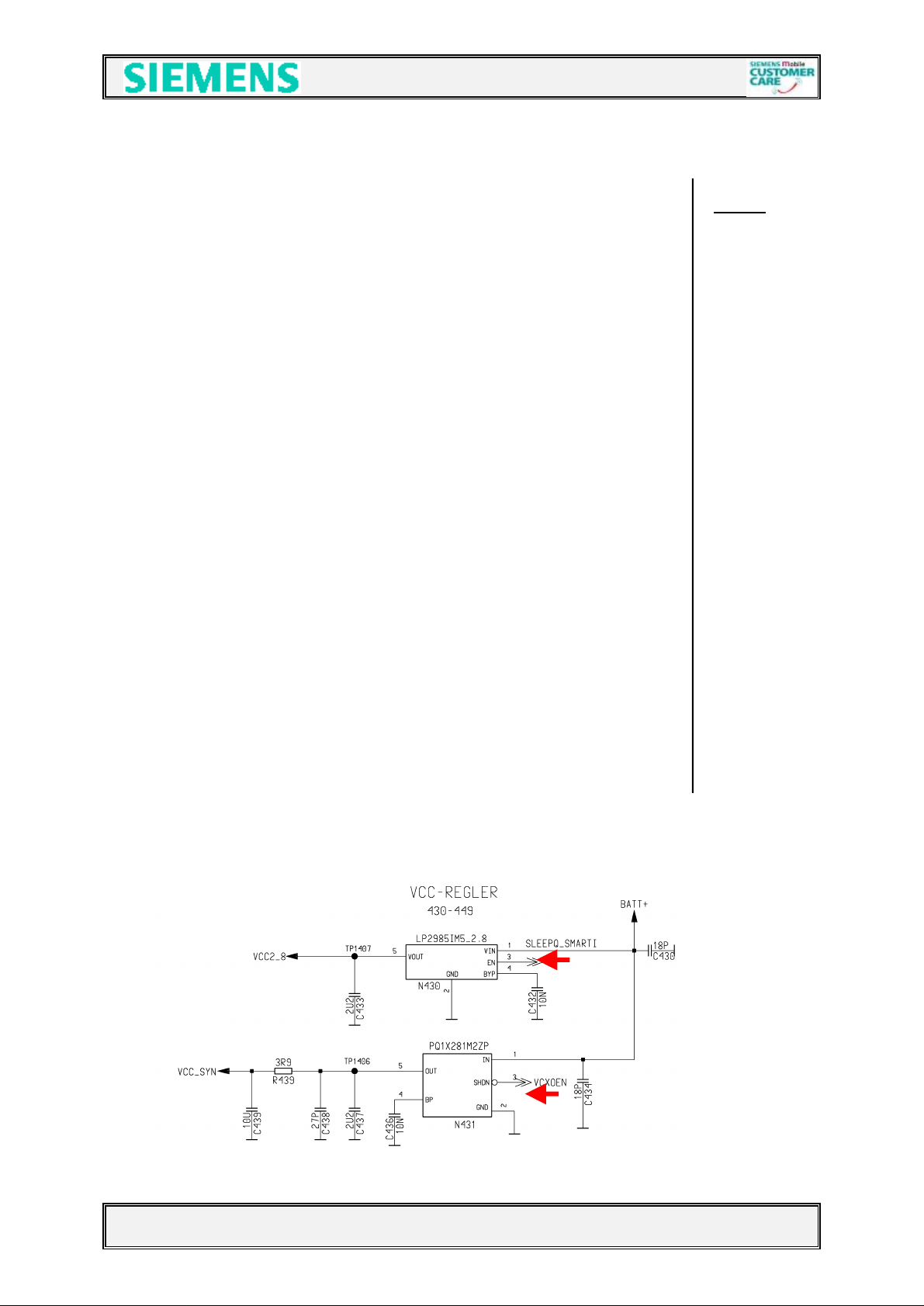
Two voltage regulators (N430/431) with a nominal output voltage of 2.8V are
used, to perform the required “RF-Voltages”.
The voltage regulator N430 is activated via SLEEPQ_SMARTI provided by the
EGOLD+ (TDMA-Timer H12).
The voltage regulator N431 is activated via VCXOEN provided by
the EGOLD+ (Functional P7).
The name of the voltages are: a) VCC_SYN activated by VCXOEN
and b) VCC2_8 activated by SLEEPQ_SMARTI
For both voltages BATT+ is required.
V1.0 Page 6 of 38 ICM MP CC ST
A35-A36-A40 Company Confidential 09/01
C616
100N
100N
C600
123
4211
4.2 Frequency generation
4.2.1 Synthesizer : The discrete VCXO (13MHz)
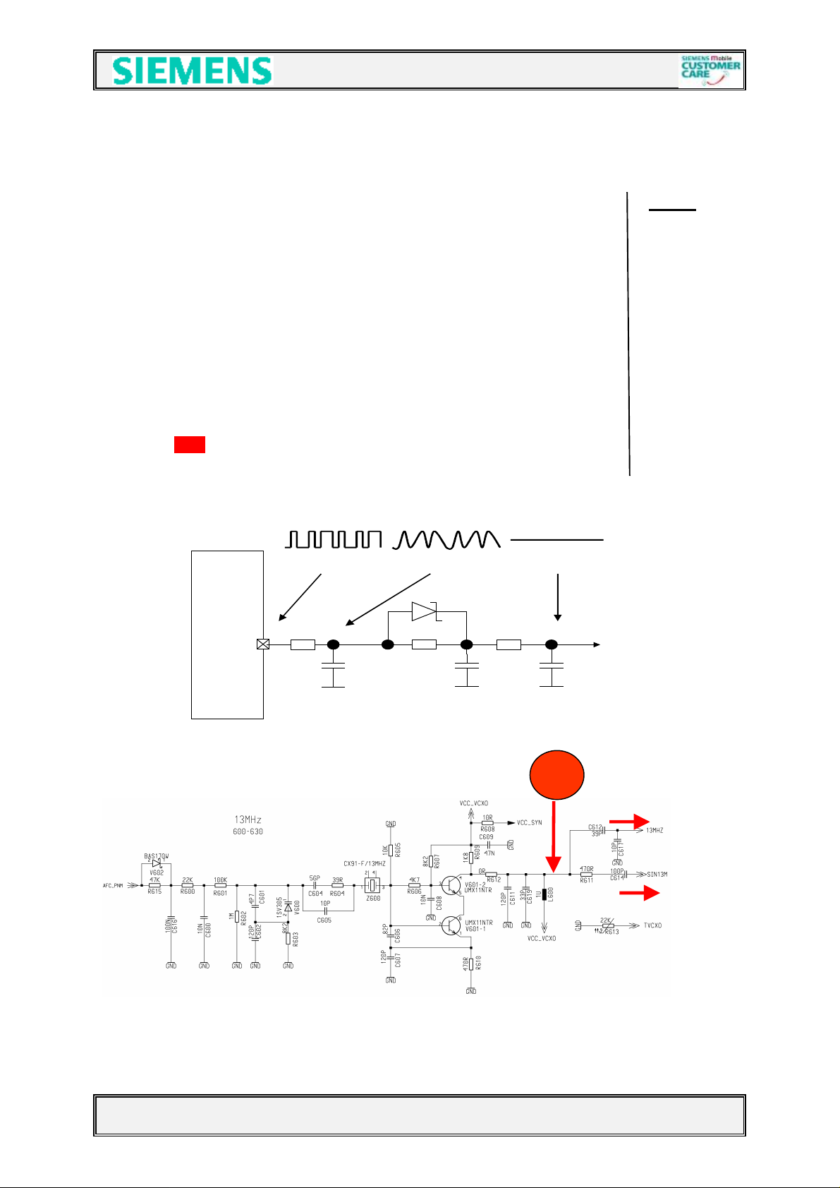
The Axx 13MHz signal is generated by a discrete VCXO. consisting of a colpitts Notes
oscillator with a crystal Z600 and a post-switched buffer stage as oscillator switch.
The subsequent oscillating circuit (C611,C619, L600) and the resistor R611
create a de-coupling of the synthesiser from interference signals, coming from the
logic (SIN13M (functional F13M)).
The oscillator frequency is controlled by the EGOLD+ (functional R3) generated
AFC_PNM signal, and the capacity diode V600, to ensure that the circuit is
working is stable conditions < 7,7ms after switching on the oscillator.
To reduce the charging time of the low pass (R615, C616) the resistor R615 is
bridged by the diode V602.
For temperature control a temperature-dependent resistor R613 is placed near the
VCXO.
The required voltage VCC_SYN is provided by the N431.
The picture 4211 shows the signal at the collector of transistor V601_2.
Signalform
EGOLD+
V1.3
V602
1 2 3
AFC
R106
30K 22K
AFC_PNM
C110
GND
BAS170W
R615
47K
GND
R600
10N
GND
to SMARTI
to EGOLD+
V1.0 Page 7 of 38 ICM MP CC ST
A35-A36-A40 Company Confidential 09/01
4221
4223
4222
4.2.2 Synthesizer : LO1
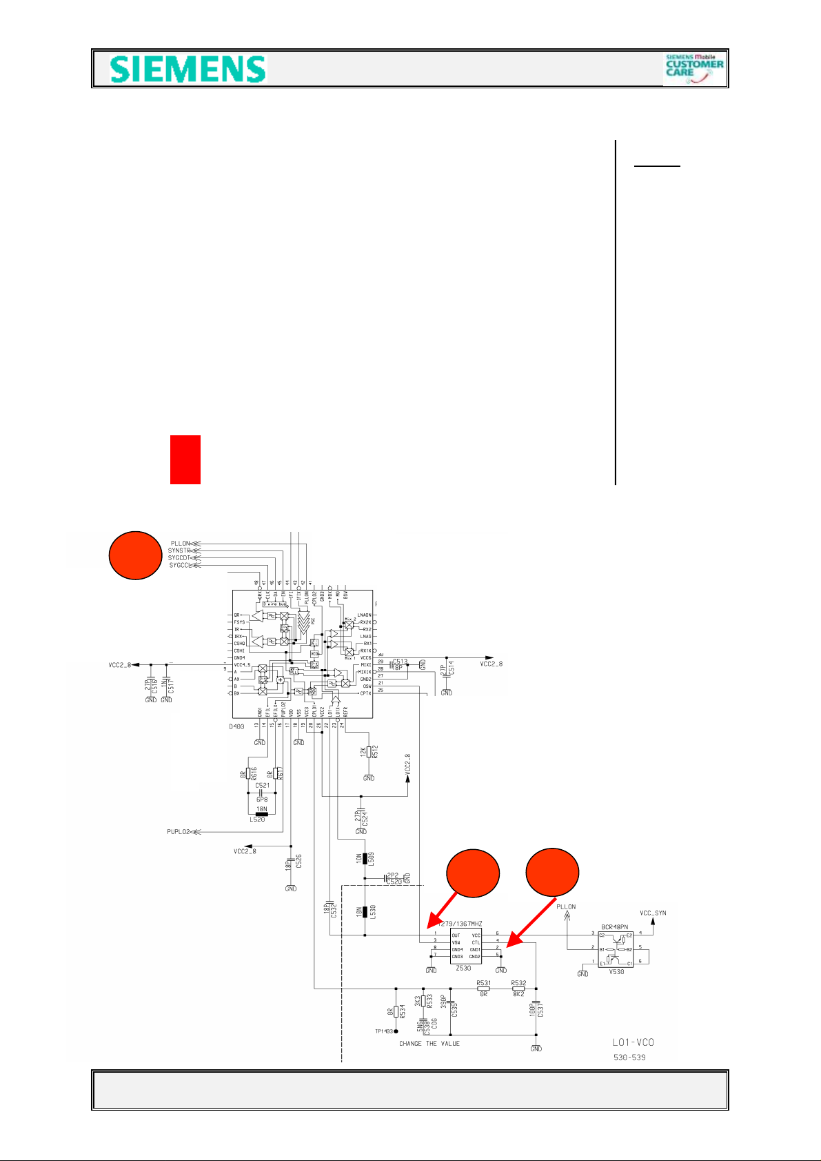
The first local oscillator (LO1) consists of the D400 PLL part, a loop filter Notes
and a VCO (Z530) module. This LO1 circuit generates frequencies from 1445MHz
to 1520MHz for GSM 1800 RX-operation, and from 1285MHz to 1361MHz
for the other operations. The Z530 is switchable to select the channels in stages of
200kHz. The VCO module is activated by the EGOLD+ signal
PLLON (TDMA-Timer J12) via V530. The switching between GSM900 and GSM1800 is
realised by the OSW signal from the SMARTI (D400 pin 21),
The channel programming happens via the EGOLD+. signals SYGCCL, SYGCDT,
SYNSTR.
The VCO output signal fulfils three functions:
a) It enables the SMARTI IC to mix the RXIF-Frequency (360 MHz)
b) It enables the SMARTI IC to mix the TXIF-Frequency (424 MHz)
c) It ensures with the help of the 13MHz signal and the SMARTIs PLL part the
frequency stability by generating a control voltage at (SMARTI pin 20)
The required voltages are: VCC2_8 for D400 provided by N430.
VCC_SYN for the VCO provided by N431
The picture 4221 shows the VCO output signal
The picture 4222 shows the control voltage
The picture 4223 shows the programming signals for the PLL
V1.0 Page 8 of 38 ICM MP CC ST
A35-A36-A40 Company Confidential 09/01
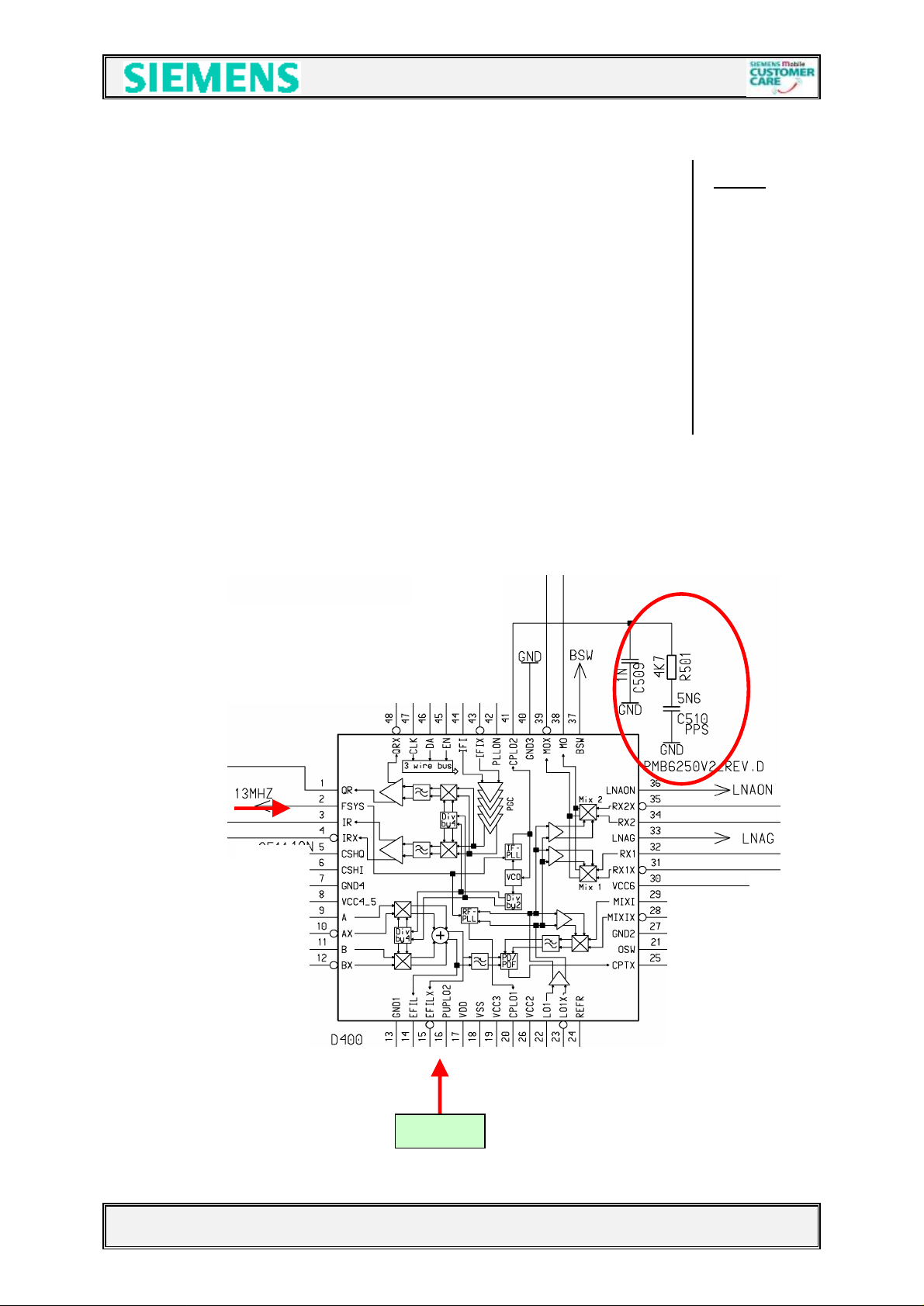
4.2.3 Synthesizer : LO2
The second local oscillator (LO2) consists of: Notes
a) the SMARTIs (D400) PLL part
b) the 13MHz reference signal
c) a switchable VCO (inside the SMARTi)
d) an external filter (C509,C510,R501).
The VCO generates 2 frequencies (1440MHz for RX-Mode and 1696 MHz for
TX-Mode).
Both frequencies are divided by 4, to get the 360MHz demodulator frequency and
the 424MHz modulator frequency.
The RX/TX switching is done internally, initiated by the EGOLD+ through the
SYGCCL, SYGCDT,SYNSTR signals.
Using the EGOLD+ signal PUPLO2 (TDMA-Timer L11) at pin 16, the second local
oscillator is switched “ON and OFF”
The required voltage VCC2_8 for D400 is provided by N430
PUPLO2
External
filter LO2
V1.0 Page 9 of 38 ICM MP CC ST
A35-A36-A40 Company Confidential 09/01
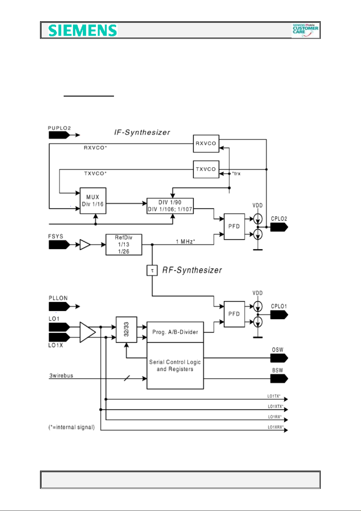
4.2.4 Synthesizer : PLL
PLL as a part of the PMB6250 (SMARTI) IC D400
Blockdiagramm
V1.0 Page 10 of 38 ICM MP CC ST
A35-A36-A40 Company Confidential 09/01
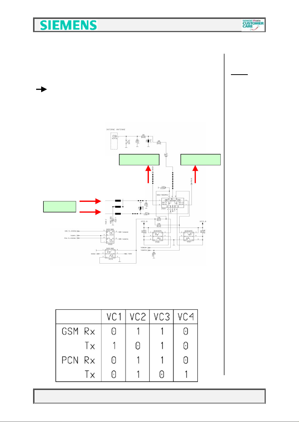
4.3 Antenna switch (electrical)
Internal > Receiver/Transmitter <> GSM900/1800
The Axx mobile has in opposite to P35 only one antenna switch (electrical). Notes
The electrical antenna switch (Diplexer Z503) is used for the differentiation
between the receiving and transmitting signals, just like the differentiation
between GSM900 and GSM1800.
To do so the transistors V506,V507,V509 and V510 are used to switch the
diplexer signals VC1–VC4 as required.
from PA
Please note, that Axx mobiles have no external antenna connector.
The matrix below shows the different conditions at the diplexer and the
accompanying signals.
to GSM receiver
to PCN receiver
V1.0 Page 11 of 38 ICM MP CC ST
A35-A36-A40 Company Confidential 09/01
4411
4412
4413
4414
4.4 Receivers
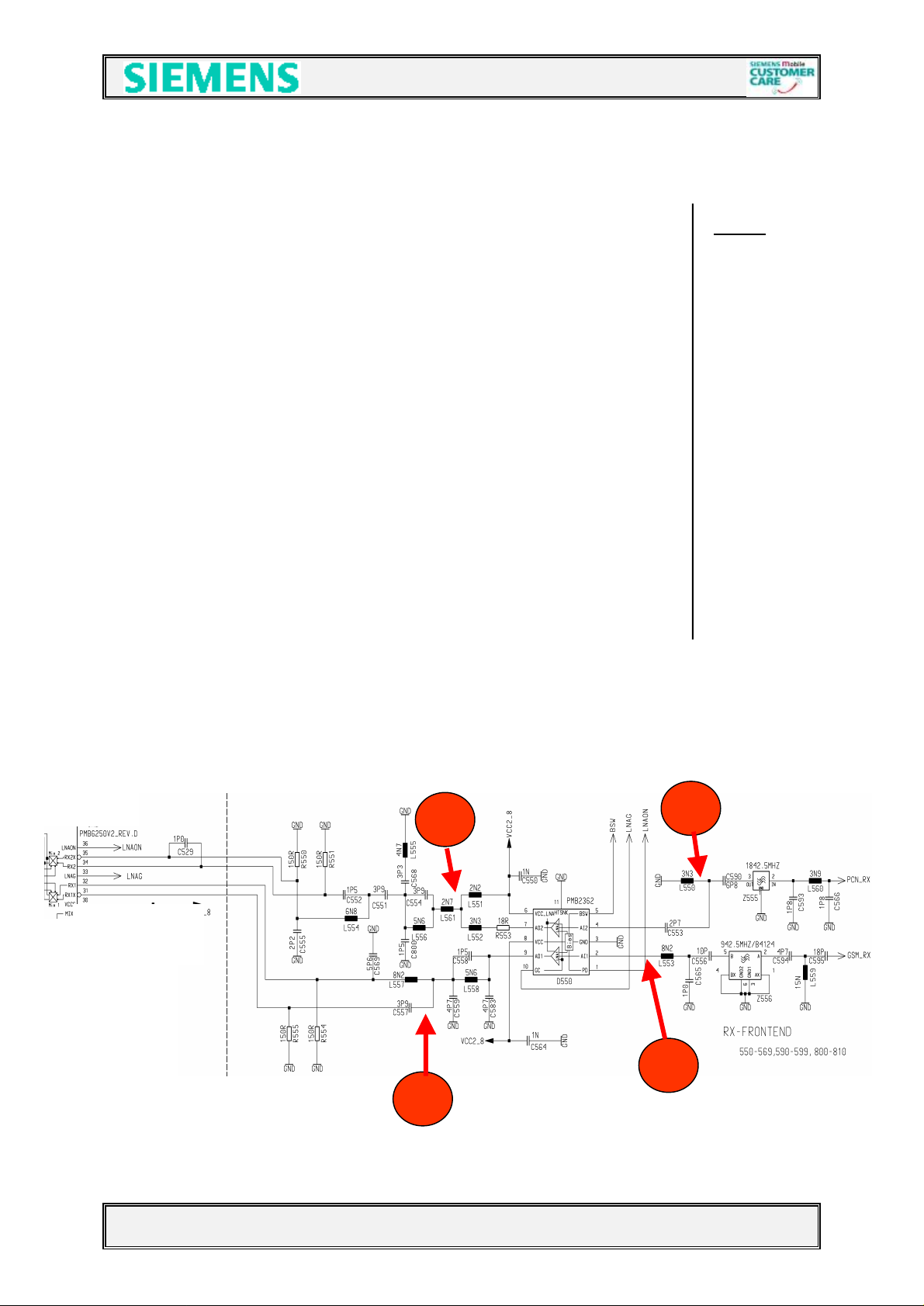
4.4.1 Receiver: GSM900/1800 Diplexer > Filter > LNA > Mixer
From the antenna switch up to the IF-Mixer, the GSM1800 receiver circuit Notes
consists of:
a) a ceramic front end filter (Z555)
b) a LNA (Low Noise Amplifier D550)
c) and a subsequent discrete distortion LC-high-pass-filter.
For GSM900 the signal flow is as follows: From the antenna switch, via a SAW filter
(Z556), through the LNA (D550) and a discrete distortion LC-low-pass-filter to the
IF-Mixer..
The amplification of both LNA´s is approx. 20dB with a matched 50 ohm output.
The LNA is switched “On” with the signal LNAON (SMARTI pin 36).
For switching between GSM1800 and GSM900 the signal BSW is generated from
the (SMARTI pin 37).
The signal LNAG (SMARTI pin 33) is in use, if the received signal level is too high.
with LNAG “active”, the LNA reduces the incoming signal in one step by 20dB
The non-symmetrical LNA output is connected to the IF mixer via a discrete
balancing and adaptation circuit. This circuit converts the asymmetrical
signal into a symmetrical signal.
The required voltage VCC2_8 is provided by N430
V1.0 Page 12 of 38 ICM MP CC ST
A35-A36-A40 Company Confidential 09/01
 Loading...