


A52, A55 & C55 IFX
Level 2.5e
Repair Documentation
V 1.10
|
Version |
|
Date |
Department |
Notes to change |
|
|
|
|
V 1.00 |
|
09.052003 |
ICM MP CCQ GRM |
New document |
|
|
|
|
V 1.10 |
|
11.08.2003 |
ICM MP CCQ GRM |
Document modified (A52) |
|
|
|
|
|
|
|
|
|
|
|
|
|
|
|
|
|
|
|
|
|
|
V 1.10 |
|
Page 1of 45 |
|
ICM MP CCQ GRM |
|
||
|
A52/A55/C55 IFX |
Company Confidential © Copyright Siemens AG |
|
08/03 |
|
|||
|
|
|
|
|
|
|
|
|

Table of Contents:
1 LIST OF AVAILABLE LEVEL 2,5E PARTS C55 IFX ......................................... |
4 |
||||
2 REQUIRED EQUIPMENT FOR LEVEL 2,5E ...................................................... |
5 |
||||
3 REQUIRED SOFTWARE FOR LEVEL 2,5E C55 IFX......................................... |
5 |
||||
4 |
RADIO PART DESCRIPTION............................................................................. |
6 |
|||
4.1 |
Introduction..................................................................................................... |
|
6 |
||
4.2 |
Power Supply RF-Part .................................................................................... |
7 |
|||
4.3 |
Frequency generation .................................................................................... |
7 |
|||
|
4.3.1 Synthesizer: The discrete VCXO (26MHz)........................................................................... |
7 |
|||
|
4.3.2 |
Synthesizer: LO1.................................................................................................................. |
8 |
||
4.4 |
Antenna Switch / External Antenna Connector (electrical/mechanical only |
||||
C55) |
10 |
|
|
|
|
4.5 |
Frontendmodul (Electrical Antenna Switch) .............................................. |
10 |
|||
4.6 |
Receiver......................................................................................................... |
|
11 |
||
|
4.6.1 Receiver: EGSM900/GSM1800 – Filter to Demodulator ................................................... |
11 |
|||
|
4.6.2 |
IC Overview |
........................................................................................................................ |
13 |
|
4.7 |
Transmitter.................................................................................................... |
|
15 |
||
|
4.7.1 Transmitter: Modulator and Limited Amplifier .................................................................... |
15 |
|||
|
4.7.2 Transmitter: and Power Amplifier....................................................................................... |
16 |
|||
5 |
LOGIC / CONTROL........................................................................................... |
17 |
|||
5.1 |
Overview of Hardware Structure ................................................................. |
17 |
|||
|
5.1.1 |
Logic Block Diagram .......................................................................................................... |
17 |
||
|
5.1.2 Block Diagram C55 IFX Control Part ................................................................................. |
17 |
|||
|
5.1.3 |
EGOLD+............................................................................................................................. |
|
18 |
|
|
5.1.4 |
SRAM ................................................................................................................................. |
|
22 |
|
|
5.1.5 |
FLASH ................................................................................................................................ |
|
22 |
|
|
5.1.6 |
SIM ..................................................................................................................................... |
|
22 |
|
|
5.1.7 |
Vibration Motor ................................................................................................................... |
23 |
||
6 |
POWER SUPPLY.............................................................................................. |
23 |
|||
6.1 |
Power Supply ASIC ...................................................................................... |
23 |
|||
|
6.1.1 Power Supply Operating modes: ....................................................................................... |
25 |
|||
|
6.1.2 |
Power Supply Functions:.................................................................................................... |
26 |
||
6.2 |
Battery ........................................................................................................... |
|
33 |
||
6.3 |
Charging Concept......................................................................................... |
34 |
|||
|
|
|
|
|
|
V 1.10 |
|
|
Page 2of 45 |
ICM MP CCQ GRM |
|
A52/A55/C55 IFX |
Company Confidential © Copyright Siemens AG |
08/03 |
|||
|
|
|
|
|
|

7 |
INTERFACES.................................................................................................... |
37 |
|
7.1 |
Vibra............................................................................................................... |
37 |
|
7.2 |
Earpiece......................................................................................................... |
37 |
|
7.3 |
Microphone ................................................................................................... |
38 |
|
7.4 |
Battery ........................................................................................................... |
38 |
|
7.5 |
IO Connector with ESD protection.............................................................. |
39 |
|
7.5.1 IO Connector – New Slim Lumberg ................................................................................... |
39 |
||
7.5.2 ESD Protection with EMI filter ............................................................................................ |
40 |
||
7.6 |
SIM ................................................................................................................. |
41 |
|
7.7 |
Display........................................................................................................... |
41 |
|
8 |
ACOUSTIC........................................................................................................ |
42 |
|
8.1 |
Microphone ................................................................................................... |
42 |
|
8.1.1 |
Mechanical ......................................................................................................................... |
42 |
|
8.1.2 |
Electrical ............................................................................................................................. |
42 |
|
8.2 |
Earpiece/Loudspeaker ................................................................................. |
43 |
|
8.2.1 |
Mechanical ......................................................................................................................... |
43 |
|
8.2.2 |
Electrical ............................................................................................................................. |
43 |
|
9 |
DISPLAY AND ILLUMINATION........................................................................ |
44 |
|
9.1 |
Display........................................................................................................... |
44 |
|
9.2 |
Illumination ................................................................................................... |
44 |
|
10 |
KEYBOARD ................................................................................................... |
45 |
|
V 1.10 |
Page 3of 45 |
ICM MP CCQ GRM |
A52/A55/C55 IFX |
Company Confidential © Copyright Siemens AG |
08/03 |
|
|
|

1 List of available level 2,5e parts C55 IFX
ID-No |
Type |
Board |
Name, Location |
Part-No. |
D150 |
VCO |
HIT |
Transmitter_VCO |
L36820-L6097-D670 |
D1600 |
VCO |
IFX |
Transmitter_VCO |
L36820-L6109-D670 |
D171 |
IC |
HIT/IFX |
Egold+ |
L36810-G6149-D670 |
D1740 |
Filter |
IFX |
Ant_Switch_Diplexer |
L36197-F5006-F936 |
D1785 |
IC |
IFX |
Transceiver IC |
L36197-F5011-F334 |
D361 |
IC |
HIT/IFX |
ASIC |
L36145-J4682-Y43 |
D800 |
IC |
HIT |
Transceiver IC |
L36820-L6105-D670 |
D920 |
IC |
HIT |
PA_Comperator |
L36820-L6133-D670 |
R1507 |
Resistor |
IFX |
Temp_Resistor |
L36120-F4223-H |
R959 |
Resistor |
HIT |
Temp_Resistor |
L36120-F4223-H |
V1500 |
Diode |
IFX |
Capa_Diode |
L36840-D61-D670 |
V151 |
Diode |
HIT/IFX |
Diode_KB7 |
L36840-D5062-D670 |
V181 |
Diode |
HIT/IFX |
Diode_Battery_Interface |
L36702-A1051 |
V211 |
Transistor |
HIT/IFX |
Tran._Vibra |
L36830-C1097-D670 |
V220 |
Diode |
HIT/IFX |
Diode_Vibra |
L36851-Z9105-Z981 |
V222 |
Transistor |
HIT/IFX |
Trans_Light_ |
L36830-C1112-D670 |
V223 |
Transistor |
HIT |
Trans_Light_ |
L36840-C4004-D670 |
V361 |
Transistor |
HIT/IFX |
Tran._Charge |
L36830-C1110-D670 |
V850 |
Transistor |
HIT |
Tran._VCO_Switch |
L36820-C6047-D670 |
V920 |
Diode |
HIT |
Feedback_Diode |
L36840-D5049-D670 |
V921 |
Transistor |
HIT |
Tran._PA_Switch |
L36820-C6047-D670 |
V950 |
Transistor |
HIT |
Tran._26MHz_Ampl. |
L36840-C4049-D670 |
V951 |
Diode |
HIT |
Capa_Diode |
L36840-D61-D670 |
Z1500 |
Quartz |
IFX |
Oszillator_26MHz |
L36145-F260-Y17 |
Z1600 |
Filter |
IFX |
Transmitter_Filter |
L36145-K280-Y242 |
Z1700 |
IC |
IFX |
Power_Amplifier |
L36197-F5005-F487 |
Z171 |
Quartz |
HIT/IFX |
Quarz/Egold |
L36145-F102-Y8 |
Z211 |
Filter |
HIT/IFX |
Logic/IO_Interface |
L36197-F5000-F116 |
Z850 |
VCO |
HIT |
1LO_VCO |
L36145-G100-Y96 |
Z851 |
Filter |
HIT |
Filter_BALUN |
L36145-K260-Y41 |
Z880 |
IC |
HIT |
Ant_Switch_Diplexer |
L36145-K280-Y257 |
Z900 |
IC |
HIT |
Power_Amplifier |
L36851-Z2002-A59 |
Z950 |
Quartz |
HIT |
Oszillator_26MHz |
L36145-F260-Y17 |
V 1.10 |
Page 4of 45 |
ICM MP CCQ GRM |
A52/A55/C55 IFX |
Company Confidential © Copyright Siemens AG |
08/03 |
|
|
|

2 Required Equipment for Level 2,5e
-GSM-Tester (CMU200 or 4400S incl. Options)
-PC-incl. Monitor, Keyboard and Mouse
-Bootadapter 2000/2002 (L36880-N9241-A200)
-Adapter cable for Bootadapter due to new Lumberg connector
-Troubleshooting Frame C55 (F30032-P209-A1)
-Power Supply
-Spectrum Analyser
-Active RF-Probe incl. Power Supply
-Oscilloscope incl. Probe
-RF-Connector (N<>SMA(f))
-Power Supply Cables
-Dongle (F30032-P28-A1) if USB-Dongle is used a special driver for NT is required
-BGA Soldering equipment
Reference: Equipment recommendation V1.2 (downloadable from the technical support page)
3 Required Software for Level 2,5e C55 IFX
-Windows NT Version4
-Winsui version1.43 or higher
-Software for GSM-Tester ( Cats(Acterna/Wiltek) or CMU-GO(Rohde&Schwarz) )
-Software for reference oscillator adjustment
-Internet unblocking solution
-Dongle driver for USB-Dongle if used with WIN NT4
V 1.10 |
Page 5of 45 |
ICM MP CCQ GRM |
A52/A55/C55 IFX |
Company Confidential © Copyright Siemens AG |
08/03 |
|
|
|

4 Radio Part Description
4.1 Introduction
The radio part is necessary to convert the GMSK-RF-signals from the antenna to the baseband and vice versa.
In the receiving direction, the signals are split in the I- and Q-component and fed to the A/D-converter of the logic part. In the transmission direction, the GMSK-signal is generated with the Direct Modulator by modulation of the I- and Q-signals, which are generated in the baseband section. After the modulation the RF-signals are amplified by a buffer-limiter and, for the GSM900 path, filtered with a SAW-Filter. Finally, the power amplifier (PA) is attached to reach the output power.
Transmitter and Receiver are never active at the same time. Simultaneous reception in the EGSM 900 and GSM 1800 band is impossible as well as simultaneous transmission in both bands. However the monitoring band (monitoring timeslot) in the TDMA-frame can be chosen independently of the receiving or transmitting band (RXand TX timeslot of the band).
The RF-part is designed for dualband operation (EGSM 900, GSM 1800) and consists of the following main components:
1.26MHz reference crystal Z1500
2.TX-Filter in GSM section Z1600
3.Transmitter power amplifier RF9340 with integrated regulator Z1700
4.Front-End-Module including RX-/TX-switch and EGSM 900/GSM1800 receiver SAWfilters D1740
5.Infineon Limiter/Buffer PMB2256 to amplify the RF signals from the modulator to drive the PA D1600
6.Infineon Smarti DC2 PMB6256 with the following functionality D1785:
•Integrated active part of the 26MHz crystal oscillator
•PLL for local oscillator LO1
•LO1-VCO
•Direct conversion receiver with channel filtering
•Direct Modulator
•Active part of the reference oscillator including buffer
•Control circuit for band switch
V 1.10 |
Page 6of 45 |
ICM MP CCQ GRM |
A52/A55/C55 IFX |
Company Confidential © Copyright Siemens AG |
08/03 |
|
|
|
4.2 Power Supply RF-Part
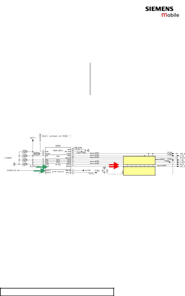
The voltage regulator for the RF-part is located inside the ASIC D361.(see chapter 5.2).It generates the required 2,85V “RF-Voltages” named VCC2_8 and VCC_SYN. (VCC_SYN is also named VCC2 and behind R1451 VCC_OSC)
The following components are supplied by:
VCC2_8 |
VCC_SYN |
|
• Limiter amplifier |
• |
Modulators |
|
• |
RX mixers |
|
• |
VCO |
|
• |
PLL |
• 26 MHz reference oscillator
The voltage regulator RFREG 1 is controlled by the signal SLEEPQ (RF_EN (RF REG G2)), RFREG2 is controlled by he signal VCXOEN_UC connected to SLEEP1_N
H1). Both signals are provided by the EGOLD+ (SLEEPQ (GSM TDMA-Timer H16) /
VCXOEN_UC (Miscellaneous R6)).
Circuit diagram
VCC2_8
VCC_SYN
4.3 Frequency generation
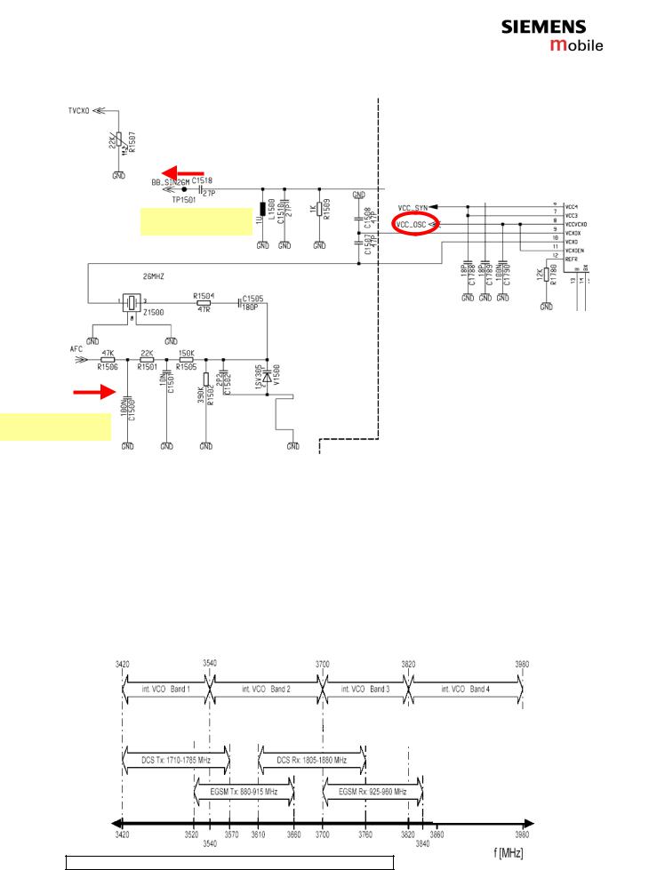
4.3.1Synthesizer: The discrete VCXO (26MHz)
The reference oscillator is a 26 MHz voltage controlled crystal oscillator. It has two main tasks:
•It is used as reference for the synthesizer phase/frequency detector (Smarti internal circuit)
•It gives the clock for the processor (E-Gold)
The main block is realized as an internal transistor cell with a Colpitts structure. The 26 MHz quartz crystal is connected to a tuning circuit that allows a fine-tuning of the frequency. A current mirror, acting as buffer and amplifier followed by a LC resonant circuit makes the signal to fit the E-Gold clock signal requirements. ON/OFF signal (VCC_OSC) comes from the ASIC via the resistor R1451. For temperature measurements of the VCXO a temperature resistance (R700) is used. The resistor is placed near the VCXO. The measurement result TVCXO is reported to the EGOLD+ (Analog Interface P3) via R138 as the signal TENV. The frequency of the reference oscillator can be adjusted by the EGOLD+ via a PNMmodulated AFC-signal.
The signal leaves the SMARTI as BB_SIN26M at pin 4 to be further used from the EGOLD+ (D171 (functional T3)).
The required voltage VCC_SYN is provided by the ASCI D361
V 1.10 |
Page 7of 45 |
ICM MP CCQ GRM |
A52/A55/C55 IFX |
Company Confidential © Copyright Siemens AG |
08/03 |
|
|
|
Circuit diagram
to EGOLD+
from EGOLD
4.3.2Synthesizer: LO1
The local oscillator (LO1) consists of a PLL inside the Smarti DC (D720), an external loop filter. The VCO is build in.
The first local oscillator is needed to generate frequencies which enables the transceiver IC to demodulate the receiver signal and to perform the channel selection in the TX part. The LO1/PLL part is switched on with PLLON (pin 5) from the EGOLD+ (D171 (GSM TDMA Timer F16)). The PLL settings are programmed by the 3 wire bus RFCLK (pin 1), RFDATA (pin2) and RFSTR (pin3). The LO frequency is 4 times the RX/TX frequency for EGSM 900 and 2 times for GSM1800.
This LO1 frequency range
The required voltage VCC_SYN is provided by the ASIC D361
|
V 1.10 |
Page 8of 45 |
ICM MP CCQ GRM |
|
|
A52/A55/C55 IFX |
Company Confidential © Copyright Siemens AG |
08/03 |
|
|
|
|
|
|
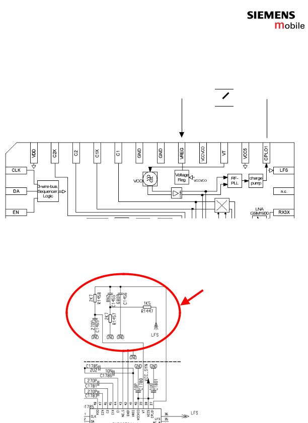
Block diagram
External
loopfilter

 ~
~

Circuit diagram
External loopfilter
|
V 1.10 |
Page 9of 45 |
ICM MP CCQ GRM |
|
|
A52/A55/C55 IFX |
Company Confidential © Copyright Siemens AG |
08/03 |
|
|
|
|
|
|
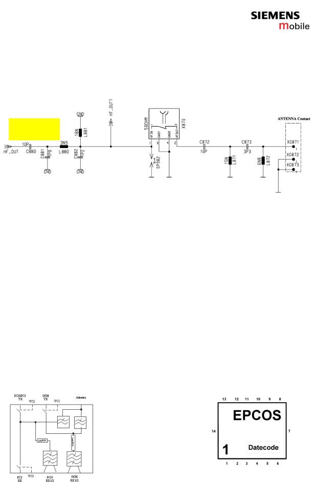
4.4 Antenna Switch / External Antenna Connector
(electrical/mechanical only C55)
The mechanical antenna switch for the differentiation between the internal and external antenna.
External |
|
Internal |
|
|
|
|
|
|
to / from diplexer
4.5 Frontendmodul (Electrical Antenna Switch)
EGSM900/GSM1800 <> Receiver/Transmitter
The frontend has two functions.
-to select the different GSM bands
-to switch between RX and TX mode
Inside the frontendmodul SAW filters are integrated in the RX paths.
For dual band mode the FEM needs two supply voltages (VC1, VC2) that are directly provided by the Smarti DC (FEM1 and FEM2). The following logical table shows the different modes of the FEM.
Mode Selection |
Vc. 1 |
Vc.2 |
Vc.3 |
EGSM900 RX |
LOW |
LOW |
LOW |
EGSM900 TX |
HIGH |
LOW |
LOW |
GSM1800 RX |
LOW |
LOW |
LOW |
GSM1800 TX |
LOW |
HIGH |
LOW |
GSM1900 RX |
LOW |
LOW |
HIGH |
GSM1900 TX |
LOW |
HIGH |
LOW |
Two balanced SAW filters are integrated to have good stop-band attenuation in the GSM and the PCN RX paths.
Top View
Block diagram
V 1.10 |
Page 10of 45 |
ICM MP CCQ GRM |
A52/A55/C55 IFX |
Company Confidential © Copyright Siemens AG |
08/03 |
|
|
|
from |
|
|
|
|
to Antenna |
PA |
|
|
|
|
|
|
|
|
|
||
|
|
|
|
Control Signals from Smarti
to Demodulator
4.6 Receiver
4.6.1Receiver: EGSM900/GSM1800 – Filter to Demodulator
From the antenna switch, up to the demodulator the received signal passes the following blocks to get the demodulated baseband signals for the EGOLD+:
Filter 

 LNA
LNA
Demodulator PGC
Inside Z650 |
Smarti |
Smarti |
Smarti |
Filter: The EGSM900, GSM1800 filters are located inside the frontend module. The Filter are centred to a frequency of 942,5MHz for EGSM900, 1847,5MHz for GSM1800.
LNA: The LNA´s (EGSM900/GSM1800) are located inside the Smarti. The LNA can be switched in HIGH (On) and LOW (Off) mode and is controlled by the Smarti depending on EGOLD+ information.
Demodulator: The Smarti DC consists of a direct conversion receiver for GSM 900/1800. The amplified RF signal is converted by a quadrature demodulator to the final outputsignals at baseband frequency. The LO signals are generated by a divider by 4 for the GSM900 band and by a divider by 2 for GSM1800 band.
The resulting in-phase and quadratursignals are fed into two baseband low pass filters and the PGC amplifier chain. The baseband filter provide a suppression of inband-blocking and adjacent channel interferers.
PGC: After baseband filtering the signal is fed into a PGC amplifier chain. The baseband amplifier offers 78 dB programmable gain with 2 dB steps. Due to the high baseband gain (58 dB), DC offsets can corrupt the signal at the baseband outputs. Differential offset voltages are reduced by an internal offset compensation circuit. The control is realised through the EGOLD+ signals (RFDATA; RFCLK; RFSTR.(RF Control J15, J16, J17).
|
|
|
|
|
|
V 1.10 |
Page 11of 45 |
ICM MP CCQ GRM |
|
|
A52/A55/C55 IFX |
Company Confidential © Copyright Siemens AG |
08/03 |
|
|
|
|
|
|
The required voltage VCCSYN is provided by the ASIC D361
Circuit diagram
progr. signals
from antenna
to EGOLD+
Top view
PMB6256
V 1.10 |
Page 12of 45 |
ICM MP CCQ GRM |
A52/A55/C55 IFX |
Company Confidential © Copyright Siemens AG |
08/03 |
|
|
|

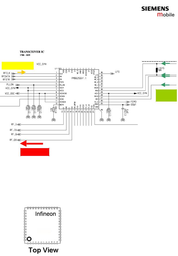
4.6.2IC Overview
IC Overview
Smarti
RX Path
TX Path
RX/TX Path
V 1.10 |
Page 13of 45 |
ICM MP CCQ GRM |
A52/A55/C55 IFX |
Company Confidential © Copyright Siemens AG |
08/03 |
|
|
|
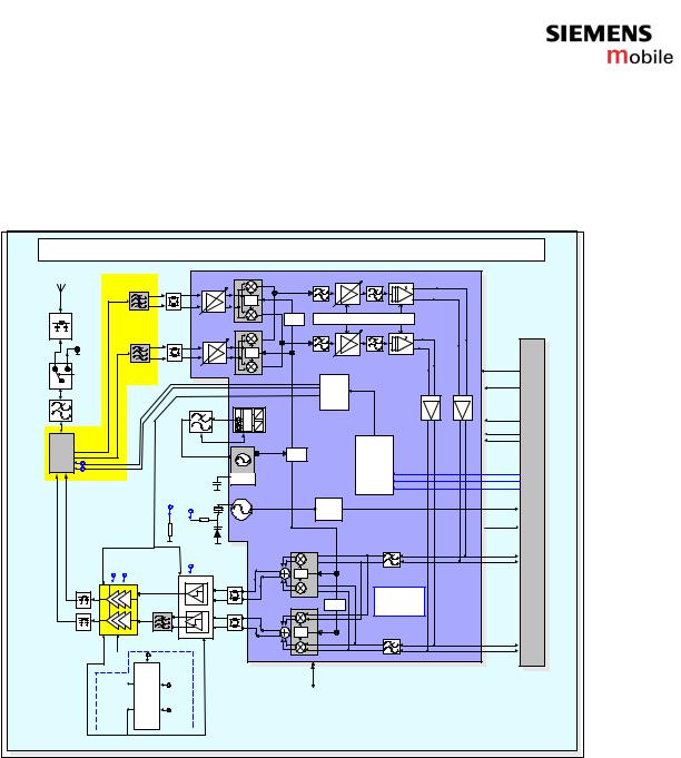
Block diagram
The functional block diagram shows the IFX RF solution of the A55/C55
|
|
|
RF-Part of L55 Tuna / Infineon |
|
|
|
|||
|
|
|
|
|
|
PGC (2dB steps) |
PGC(2dB steps) |
|
|
internal |
SAW |
|
|
|
|
BB filter |
BB filter |
|
|
|
|
|
|
|
|
|
|
||
antenna |
|
|
|
|
|
|
|
|
|
925-960 MHz |
|
|
|
|
|
|
|
|
|
|
|
|
|
|
|
|
|
|
|
|
|
|
|
+/- 45° |
|
|
|
|
|
|
942.5 MHz |
GSM LNA |
|
|
Divider |
DC autocalibration |
|
|
|
antenna |
|
(-20dB at low |
|
|
%2 |
|
|
||
FEM incl. |
gain) |
IQ demodulator |
|
|
|
|
|||
matching |
|
|
|
|
|
|
|
|
|
|
SAW |
|
|
|
|
|
|
|
|
external |
SAW |
|
|
|
|
|
|
|
|
|
|
|
|
|
|
|
|
|
|
antenna |
|
|
|
+/- 45° |
|
BB filter |
BB filter |
|
|
|
|
|
|
|
|
PGC(2dB steps) |
PGC (2dB steps) |
|
|
mechanical |
1842.5 MHz |
DCS LNA |
|
|
|
|
|
|
PLL_ON |
antenna |
1805 - 1880 MHz |
(-20dB at low |
|
|
|
|
|
|
|
gain) |
IQ demodulator |
|
|
|
|
|
|||
switch |
|
|
FEM1 |
|
|
|
|
||
|
|
|
|
Logic |
|
|
AFC |
||
|
|
|
|
|
|
|
|
||
|
|
|
|
|
FEM2 |
|
|
|
|
|
|
|
|
|
Outputs |
|
|
|
|
|
|
|
|
RF PLL |
OSW1 |
|
|
|
|
Antenna |
|
LOOP-Filter |
|
|
|
|
|
||
|
|
|
|
|
|
|
|||
low pass |
|
|
CP |
PFD R |
|
|
|
|
|
filter |
|
|
+ |
1 |
|
|
|
|
PA_RAMP |
|
|
|
|
|
|
|
|||
|
|
|
|
|
|
|
|
||
|
|
|
|
D |
|
|
BB-Out |
BB-Out |
|
|
|
LFS |
|
1 |
|
|
TXON1 |
||
|
|
|
|
|
|
|
|
TXONPA |
|
|
|
for fast lock |
|
|
|
|
|
|
|
Pin-diode |
|
|
|
|
|
|
|
|
|
|
State |
|
switch incl. |
|
|
|
|
|
Tune voltage within 0.5..2.3V |
|
Divider |
|
machine |
|
|
TX harmonic |
|
TX_GSM |
|
internal |
%2 |
|
|
|||||
filtering |
|
|
|
|
|
|
|
|||||
|
|
(FEM1) |
|
|
|
RF VCO |
|
|
Serial |
|
||
|
|
TX_DCS |
|
|
|
|
VREG |
3420 - 3540 MHz |
|
|
|
|
|
|
|
|
|
|
3540.4 - 3700 MHz |
|
|
Interface |
|
||
|
|
(FEM2) |
|
|
|
|
Int. Voltage |
|
|
RFSTR |
||
|
|
|
|
|
|
Regulator |
3700.4 - 3820 MHz |
|
|
|
||
|
|
|
|
|
|
|
|
3820.8-3839.2 MHz |
|
|
|
RFCLK |
|
|
|
|
|
|
|
|
|
|
|
|
RFDATA |
|
|
|
|
|
Tenv |
AFC voltage |
|
|
Buffer |
|
|
|
|
|
|
|
|
(from E-Gold) |
|
|
|
SIN 26MHz |
|||
|
|
|
|
|
(Temp |
|
|
|
||||
|
|
|
|
|
sensor) |
|
|
VCXO |
|
26MHz |
|
TVCXO |
|
|
|
|
|
|
|
|
|
|
|
||
|
|
|
|
|
|
|
integrated active |
|
|
|
(Tenv) |
|
|
|
|
|
|
|
|
|
part |
|
|
|
|
|
|
|
|
OSW1 |
|
|
|
26 MHz |
|
|
|
|
|
|
|
|
|
|
|
|
|
|
|
|
|
|
|
|
|
(Low=GSM |
|
|
|
|
|
|
|
|
|
|
|
|
High=DCS) |
|
|
|
|
|
|
|
|
|
|
|
|
|
|
TXON1 |
Buffer-Limiter |
|
|
|
|
BB: RF_I |
|
|
|
PA_Ramp |
Band |
|
|
|
|
|
|||
|
|
TXONPA |
(enable) |
PMB2256 |
|
|
|
|
BB: RF_IX |
|||
|
|
(200mV for |
(Low=GSM |
|
|
|
|
|
||||
|
Band |
(enable) |
lowest output |
High=DCS) |
|
(Lumpi) |
|
+/- 45° |
|
RC-Lowpass |
|
|
|
(Low=GSM |
|
|
level) |
|
|
|
|
|
|
|
|
|
High=DCS) |
|
|
|
|
|
|
|
|
|
|
|
|
|
|
|
|
DCS |
|
|
|
|
|
Transceiver IC |
|
|
|
|
|
|
|
|
|
|
|
Divider |
|
|
PCN |
|
|
|
|
|
|
|
|
IQ modulator |
Smarti DC2 |
|
|
|
|
|
|
|
|
|
|
|
|
%2 |
PMB6256 |
|
|
|
|
|
|
|
|
|
|
|
|
|
|
|
|
|
|
GSM |
|
|
|
|
|
|
|
|
GSM |
|
|
|
|
|
|
|
|
|
|
|
|
|
|
|
|
|
SAW |
|
H3-Filter |
|
+/- 45° |
|
|
|
|
VCC |
|
|
VCC |
|
|
|
|
BB: RF_Q |
|||
|
|
|
|
(for mod |
|
|
|
|
||||
|
2_8 |
|
BATT+ |
2_8 |
spectrum) |
|
|
|
|
BB: RF_QX |
||
|
|
BATT+ |
|
|
|
|
IQ modulator |
|
RC-Lowpass |
|||
|
|
|
|
|
|
|
|
|
|
|
|
|
|
|
|
|
enable |
|
|
|
|
|
|
|
|
|
|
VCC_SYN |
|
enable |
|
|
|
|
|
|
|
|
|
|
|
|
|
|
|
|
|
|
|
|
|
|
|
(for Smarti |
|
V RF2 |
VCXOEN |
|
|
VCC_SYN |
|
|
||
|
|
supply) |
|
Salzburg |
|
|
|
|
|
|||
|
|
2.85V |
|
|
|
is supply for all |
|
|
||||
|
|
D0950 |
|
|
|
|
|
|
||||
|
|
|
|
|
|
|
|
Chip VCC's |
|
|
||
|
|
VCC2_8 |
|
V REF1 |
SLEEPQ |
|
|
|
|
|
|
|
V 1.10 |
Page 14of 45 |
ICM MP CCQ GRM |
A52/A55/C55 IFX |
Company Confidential © Copyright Siemens AG |
08/03 |
|
|
|
 Loading...