

Page 1
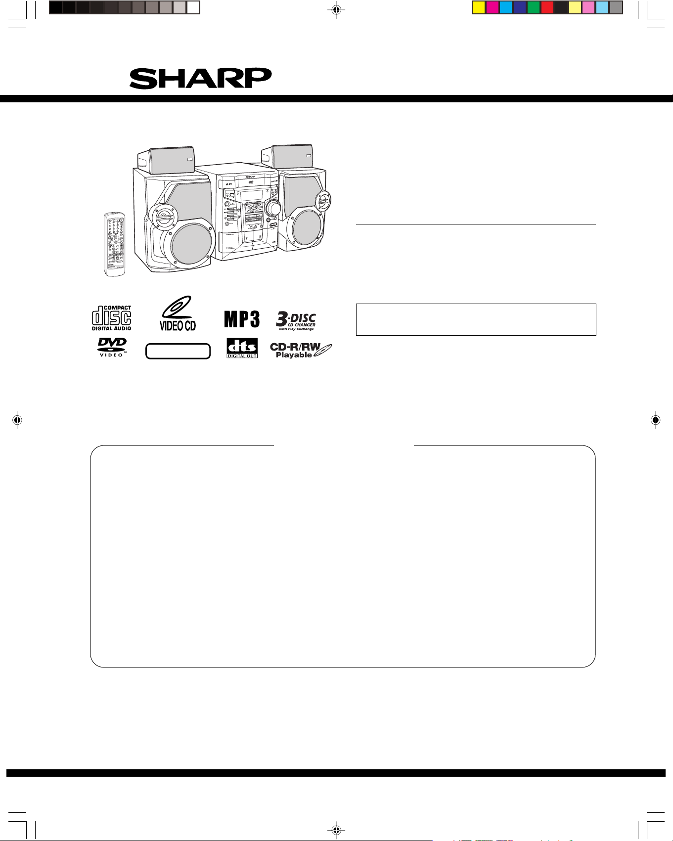
CD-E750DV
SERVICE MANUAL
No.
DVD MINI SYSTEM
MODEL CD-E750DV
CD-E750DV DVD Mini System consisting of CD-E750DV
(main unit), CP-E750DV (front speaker), and
GBOXS0133AWM1 (surround speaker).
• In the interests of user-safety the set should be restored to its
original condition and only parts identical to those specified be
used.
NTSC/PAL
CONTENTS
Page
SAFETY PRECAUTION FOR SERVICE MANUAL ........................................................................................................... 2
VOLTAGE SELECTION ..................................................................................................................................................... 2
AC POWER SUPPLY CORD AND AC PLUG ADAPTOR ................................................................................................. 2
SPECIFICATIONS ............................................................................................................................................................. 3
NAMES OF PARTS ........................................................................................................................................................... 4
DISASSEMBLY .................................................................................................................................................................. 6
REMOVING AND REINSTALLING THE MAIN PARTS ...................................................................................................... 9
ADJUSTMENT ..................................................................................................................................................................10
NOTES ON SCHEMATIC DIAGRAM .............................................................................................................................. 15
TYPES OF TRANSISTOR AND LED ............................................................................................................................... 15
BLOCK DIAGRAM ........................................................................................................................................................... 16
SCHEMATIC DIAGRAM / WIRING SIDE OF P.W.BOARD .............................................................................................. 20
VOLTAGE ........................................................................................................................................................................ 47
WAVEFORMS OF DVD CIRCUIT ................................................................................................................................... 49
TROUBLESHOOTING ......................................................................................................................................................50
FUNCTION TABLE OF IC.................................................................................................................................................53
FL DISPLAY ...................................................................................................................................................................... 68
REPLACEMENT PARTS LIST/EXPLODED VIEW
A4 (pg 01-8) 7/9/03, 2:26 PM1
SHARP CORPORATION
This document has been published to be used
for after sales service only.
The contents are subject to change without notice.
Page 2
CD-E750DV
SAFETY PRECAUTION FOR SERVICE MANUAL
WARNINGS
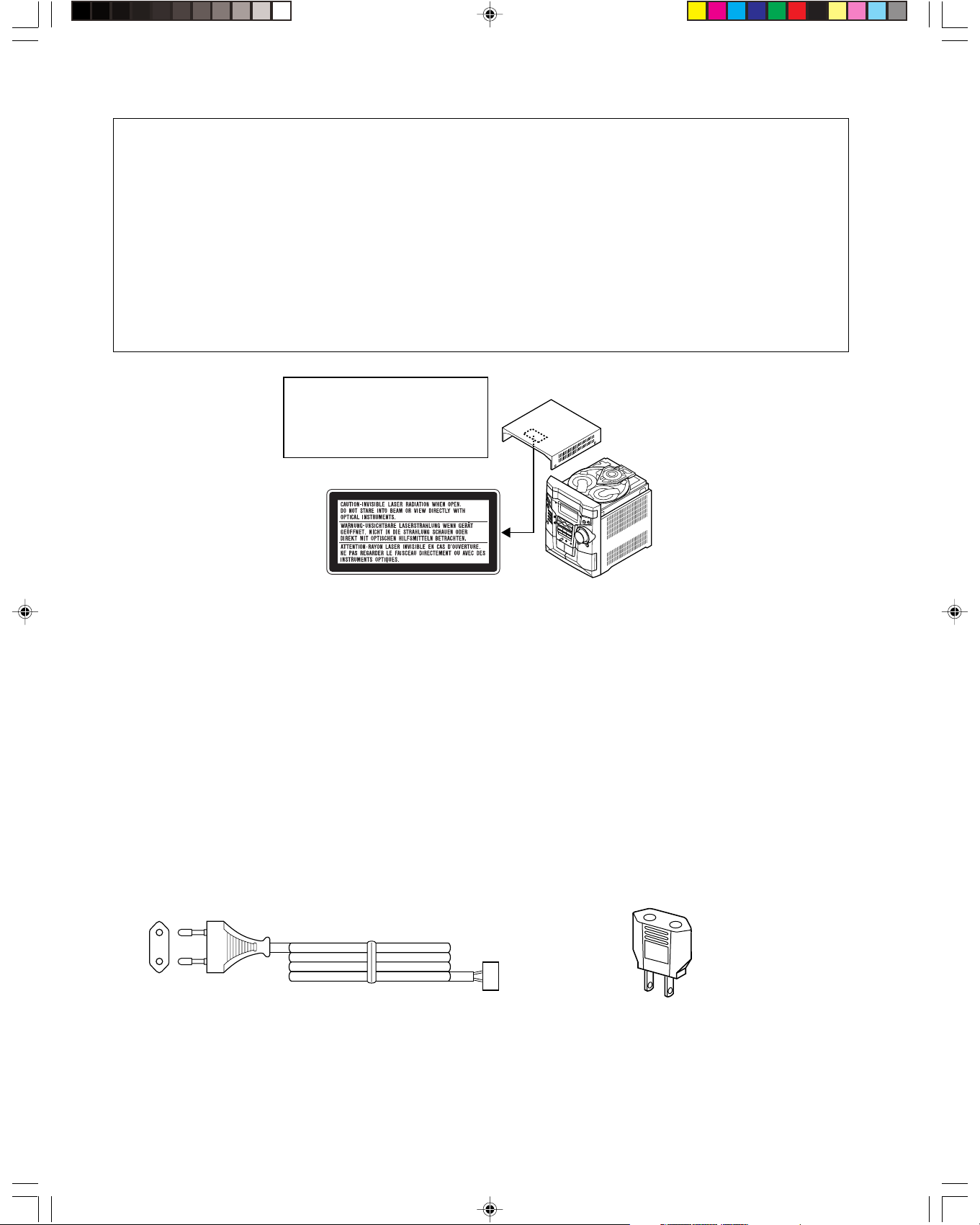
THE AEL (ACCESSIBLE EMISSION LEVEL) OF THE LASER POWER OUTPUT IS LESS THAN CLASS 1 BUT THE LASER
COMPONENT IS CAPABLE OF EMITTING RADIATION EXCEEDING THE LIMIT FOR CLASS 1. THEREFORE IT IS
IMPORTANT THAT THE FOLLOWING PRECAUTIONS ARE OBSERVED DURING SERVICING TO PROTECT YOUR EYES
AGAINST EXPOSURE TO THE LASER BEAM.
1-WHEN THE CABINET IS REMOVED, THE POWER IS TURNED ON WITHOUT A COMPACT DISC IN POSITION AND THE
PICKUP IS ON THE OUTER EDGE THE LASER WILL LIGHT FOR SEVERAL SECONDS TO DETECT A DISC. DO NOT
LOOK INTO THE PICKUP LENS.
2-THE LASER POWER OUTPUT OF THE PICKUP UNIT AND REPLACEMENT SERVICE PARTS ARE ALL FACTORY
PRESET BEFORE SHIPMENT.
DO NOT ATTEMPT TO READJUST THE LASER PICKUP UNIT DURING REPLACEMENT OR SERVICING.
3-UNDER NO CIRCUMSTANCES STARE INTO THE PICKUP LENS AT ANY TIME.
4-CAUTION-USE OF CONTROLS OR ADJUSTMENTS, OR PERFORMANCE OF PROCEDURES OTHER THAN THOSE
SPECIFIED HEREIN MAY RESULT IN HAZARDOUS RADIATION EXPOSURE.
Laser Diode Properties
Material: GaAIAs
Wavelength: 785 nm/650 nm
Emission Duration: continuous
Laser Output: max. 0.69 mW
VOLTAGE SELECTION
Before operating the unit on mains, check the preset voltage. If the voltage is different from your local voltage, adjust the voltage
as follows.
Turn the selector with a screwdriver until the appropriate voltage number appears in the window (110 V, 127 V, 220 V or 230 V - 240 V AC).
AC POWER SUPPLY CORD AND AC PLUG ADAPTOR
QACCE0015AW00
QPLGA0004AWZZ
A4 (pg 01-8) 7/9/03, 2:26 PM2
– 2 –
Page 3
FOR A COMPLETE DESCRIPTION OF THE OPERATION OF THIS UNIT, PLEASE REFER
TO THE OPERATION MANUAL.
SPECIFICATIONS
CD-E750DV
General
Power source AC 110/127/220/230 - 240 V, 50/60 Hz
Power consumption 130 W
Dimensions Width: 270 mm (10-5/8")
Weight 8.4 kg (18.5 lbs)
Amplifier
Output power
Output terminals Front speakers: 8 ohms
Input terminals Video/auxiliary (Audio input): 500 mV/47
DVD/VCD/CD player
Signal system NTSC/PAL
Supported disc types DVD(Region number 3, ALL), audio CD,
Video output Output jack: Pin jack × 1
S-video output Y output level: 1 Vp-p (75 ohms)
Video signal Horizontal resolution: 500 lines
Audio signals Frequency characteristics:
Height: 330 mm (13")
Depth: 355 mm (13-15/16")
Front speakers:
MPO: 360 W (180 W + 180 W) (10 % T.H.D.)
RMS: 170 W (85 W + 85 W) (10 % T.H.D.)
RMS: 140 W (70 W + 70 W) (0.9 % T.H.D.)
Rear speakers:
MPO: 180 W (90 W + 90 W) (10 % T.H.D.)
RMS: 80 W (40 W + 40 W) (10 % T.H.D.)
RMS: 70 W (35 W + 35 W) (0.9 % T.H.D.)
Rear speakers: 16 ohms
Headphones: 16 - 50 ohms (recommended;
32 ohms)
Audio digital out: Optical
kohms
Microphone 1/2: 1 mV/600 ohms
CD-R, CD-RW, VCD,MP3
Output level: 1 Vp-p (75 ohms)
C output level: 0.286 Vp-p (75 ohms)
Output jack: S-video connector × 1
S/N ratio: 60 dB
Linear PCM DVD:
4 Hz to 22 kHz (48 kHz sampling)/
4 Hz to 44 kHz (96 kHz sampling)
CD: 4 Hz to 20 kHz
S/N ratio: 96 dB 1 kHz (CD)
Dynamic range: 96 dB (Linear PCM DVD)
96 dB (CD)
Total harmonic distortion ratio:
0.006 % maximum
Tuner
Frequency range FM: 88 - 108 MHz
AM: 531 - 1,602 kHz
Cassette deck
Frequency
response
Signal/noise ratio 55 dB (TAPE 1, playback)
Wow and flutter 0.3 % (WRMS)
CP-E750DV
50 - 14,000 Hz (normal tape)
50 dB (TAPE 2, recording/playback)
Front speaker
Type
Maximum input
power
Rated input power 85 W
Impedance 8 ohms
Dimensions Width: 242 mm (9-9/16")
Weight 5.0 kg (11.0 lbs)/each
Twin-Drive speaker system, 50 mm(2")
tweeter and 130 mm(5-1/8") woofer x 2
170 W
Height: 330 mm (13")
Depth: 280 mm (11")
Surround speaker(GBOXS0133AWM1)
Type
Maximum input
power
Rated input power 40 W
Impedance 16 ohms
Dimensions Width: 210 mm (8-1/4")
Weight 0.7 kg (1.5 lbs)/each
Full range, 100 mm(4")
80 W
Height: 130 mm (5-1/8")
Depth: 154 mm (6-1/16")
CD-E750DV
A4 (pg 01-8) 7/9/03, 2:26 PM3
Specifications for this model are subject to change without
prior notice.
– 3 –
Page 4
CD-E750DV
CD-E750DV
Front panel
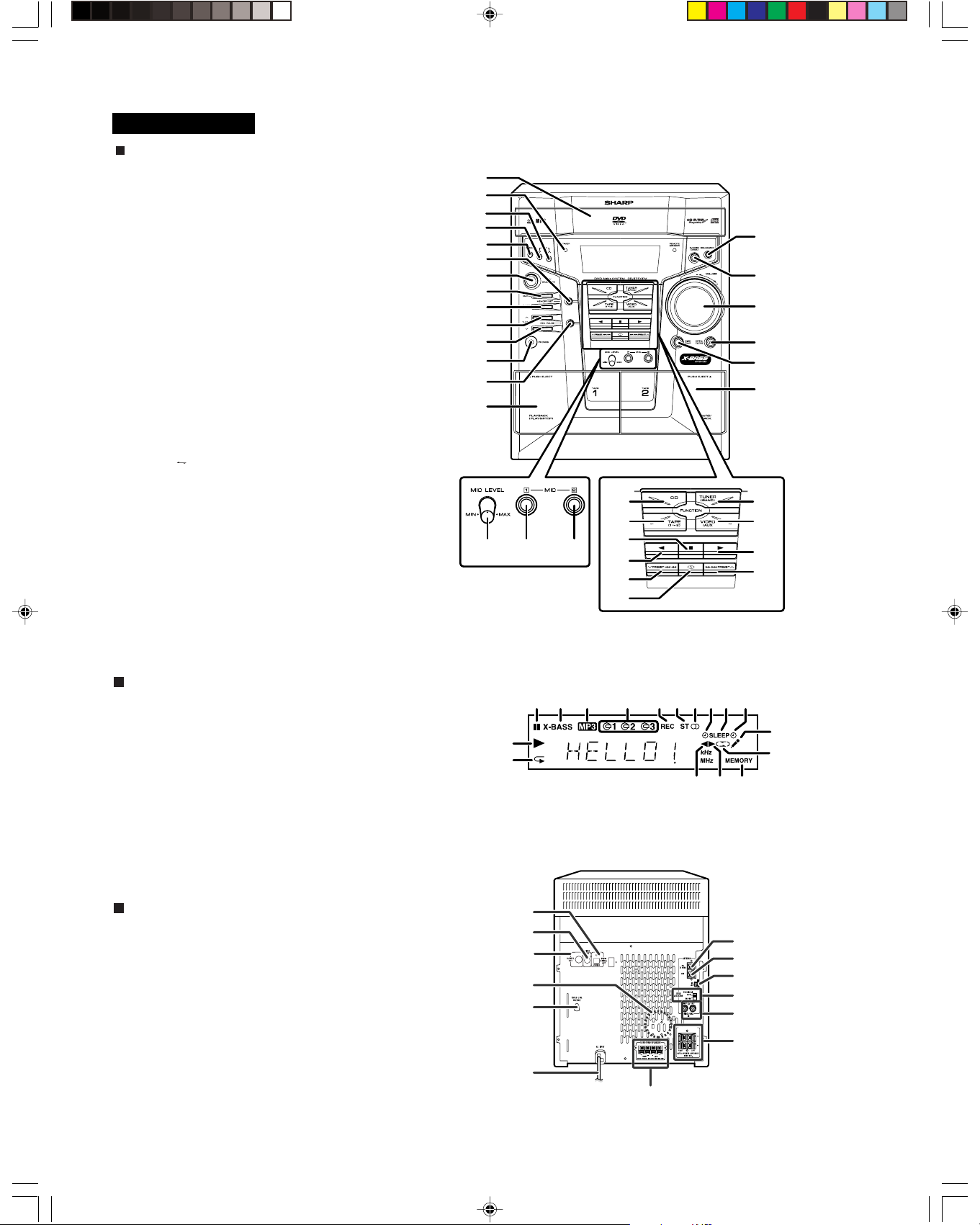
NAMES OF PARTS
1. Disc Tray
2. Timer Set Indicator
3. Echo Up Button
4. Echo Down Button
5. Karaoke Button
6. Memory/Set Button
7. On/Stand-by Button
8. Clock Button
9. Timer/Sleep Button
10. Tuning and Time Up Button
11. Tuning and Time Down Button
12. Headphone Socket
13. Tape 2 Record Pause Button
14. Tape 1 Cassette Compartment
15. Equaliser Mode Select Button
16. Extra Bass/Demo Mode Button
17. Volume Control
18. Disc Tray Open/Close Button
19. Disc Skip Button
20. Tape 2 Cassette Compartment
21. Microphone Level Control
22. Microphone Socket 1
23. Microphone Socket 2
24. DVD/Video CD/CD/MP3 Disc Button
25. Tape (1 2) Button
26. DVD/Video CD/CD/MP3 Disc/Tape Stop Button
27. Tape 2 Reverse Play Button
28. DVD Chapter Skip or Previous, DVD/Video CD/CD/MP3
Track Down or Fast Reverse, Tape 2 Fast Wind,
Tuner Preset Down Button
29. Tape 2 Reverse Mode Select Button
30. Tuner Band Button
31. Video/Auxiliary Button
32. DVD/Video CD/CD/MP3 Play,
Tape 1 Play, Tape 2 Forward Play Button
33. DVD Chapter Skip or Next, DVD/Video CD/CD/MP3
Track Up or Fast Forward, Tape 2 Fast Wind,
Tuner Preset Up Button
1
2
3
4
5
6
7
8
9
10
11
12
13
14
21 22 23
24
25
26
27
28
29
15
16
17
18
19
20
30
31
32
33
Display
1. Disc Pause Indicator
2. Extra Bass Indicator
3. MP3 Disc Indicator
4. Disc Number Indicators
5. Tape 2 Record Indicator
6. FM Stereo Mode Indicator
7. FM Stereo Receiving Indicator
8. Timer Play Indicator
9. Sleep Indicator
10. Timer Recording Indicator
11. Disc Play Indicator
12. Disc Repeat Play Indicator
13. Karaoke Mode Indicator
14. Tape Reverse Mode Indicator
15. Tape 2 Reverse Play Indicator
16. Tape 1 Play or Tape 2 Forward Play Indicator
17. Memory Indicator
Rear panel
1. Audio Digital Output
2. Video Output Socket
3. S-Video Output Socket
4. Cooling Fan
5. AC Voltage Selector
6. AC Power Lead
7. Surround Speaker Terminals
8. FM 75 Ohms Aerial Terminal
9. FM Aerial Earth Terminal
10. AM Loop Aerial Socket
11. Span Selector Switch
12. Video/Auxiliary (Audio Signal) Input Sockets
13. Front Speaker Terminal
Note:
This product is equipped with a cooling fan inside, which begins to
run at a specified volume level for better heat radiation.
11
12
2456781031 9
1
2
3
4
5
6
7
15 16 17
FRONT SPEAKERS
8
13
14
8
9
10
11
12
13
A4 (pg 01-8) 7/9/03, 2:26 PM4
– 4 –
Page 5
CD-E750DV
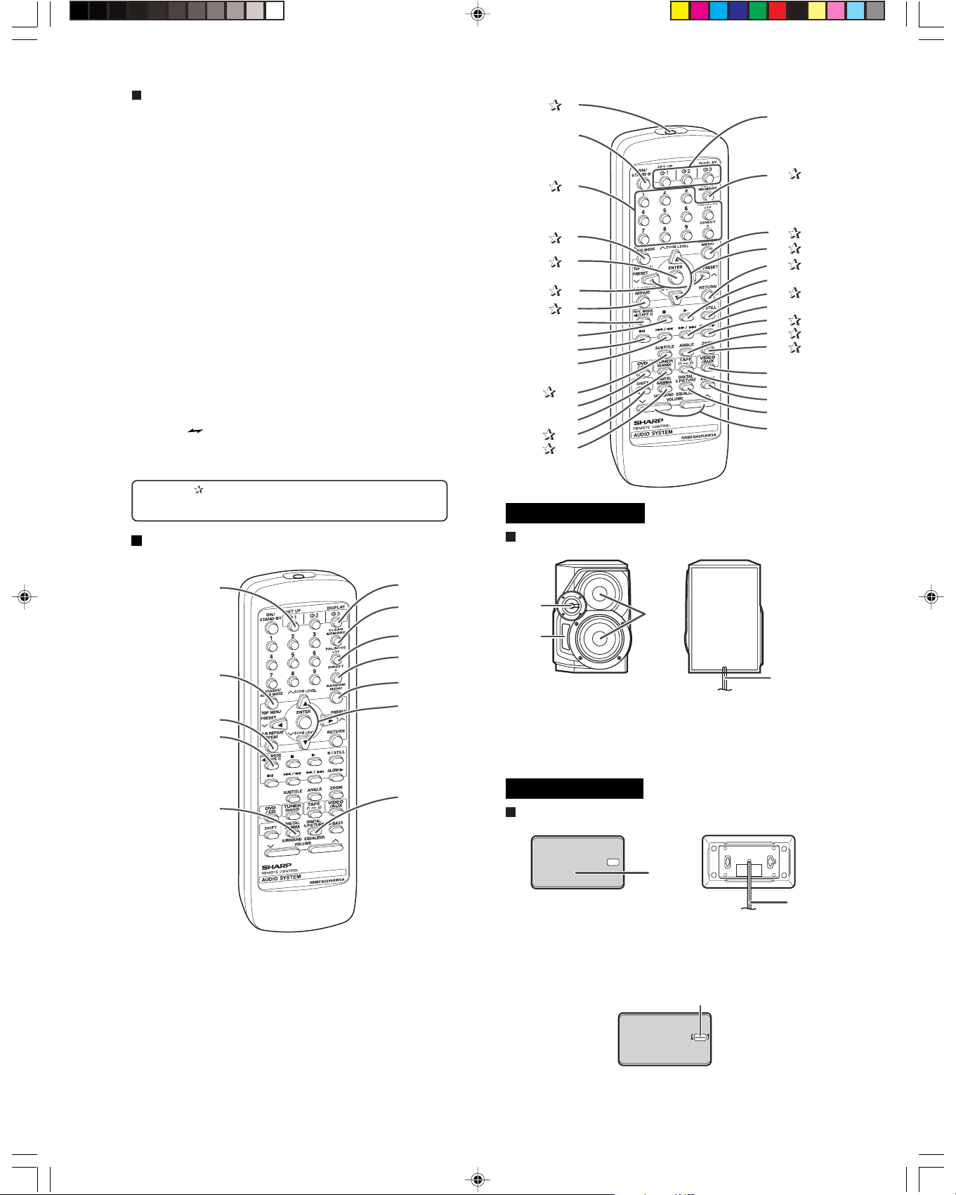
Remote control
1. Remote Control Transmitter
2. On/Stand-by Button
3. Direct Buttons
4. DVD Top Menu Button
5. Enter Button
6. Menu Select or Tuner Preset Buttons
7. DVD/Video CD/CD/MP3 Repeat Button
8. Tape 2 Reverse Play Button
9. DVD/Video CD/CD/MP3/Tape Stop Button
10. Tape 2 Record Pause Button
11. DVD Chapter Skip or DVD/Video CD/CD/Tape Fast Reverse Button
12. DVD Subtitle Button
13. DVD/Video CD/CD/MP3 Button
14. Tuner (Band) Button
15. Shift Button
16. Surround Button
17. Disc Number Select Buttons
18. DVD/Video CD/CD Memory Button
19. DVD Menu Button
20. Menu Select Buttons
21. Return Button
22. DVD/Video CD/CD/MP3/Tape Play Button
23. DVD/Video CD/CD/MP3 Pause Button
24. DVD Chapter Skip or DVD/Video CD/CD/Tape Fast Forward Button
25. DVD/Video CD Slow Button
26. DVD Angle Button
27. DVD Zoom Button
28. Video/Auxiliary Button
29. Tape (1 2) Button
30. Extra Bass Button
31. Equalizer Mode Select Button
32. Volume Up or Down Buttons
Buttons with “” mark in the illustration can be operated with the remote
control only. Other buttons can be operated on the main unit and the
remote control.
1
2
3
4
5
6
7
8
9
10
11
12
13
14
15
16
CP-E750DV
17
18
19
20
21
22
23
24
25
26
27
28
29
30
31
32
Remote control with shift button
1
2
3
4
5
1. DVD Setup Button
2. Karaoke/Audio Mode Button
3. DVD/Video CD/CD A-B Repeat Button
4. Tape 2 Reverse Mode Select Button
5. DVD Digital Gamma Button
6. DVD/Video CD/CD Display Button
7. DVD/Video CD/CD Clear Button
8. PAL/NTSC Button
9. DVD Direct Button
10. Video CD/CD Random Button
11. Echo Level Up/Down Button
12. DVD Digital Super Picture Button
6
7
8
9
10
11
12
Front Speakers
1
3
2
1. Tweeter
2. Bass Reflex Duct
3. Woofer
4. Speaker Wire
Note:
The speaker grilles are not removable.
GBOXS0133AWM1
Surrounds Speakers
4
1
1. Full-Range Speaker
2. Speaker Wire
Note:
When the surround speakers are hung on the wall, the speaker
badge will be turned. In this case, you can adjust the badge to face
the proper direction by turning it by hand.
Badge
Note:
The speaker grilles are not removable.
2
A4 (pg 01-8) 7/9/03, 2:26 PM5
– 5 –
Page 6
CD-E750DV
r
DISASSEMBLY
Caution on Disassembly
Follow the below-mentioned notes when disassembling
the unit and reassembling it, to keep it safe and ensure
excellent performance:
1. Take cassette tape and compact disc out of the unit.
2. Be sure to remove the power supply plug from the wall
outlet before starting to disassemble the unit.
3. Take off nylon bands or wire holders where they need to
be removed when disassembling the unit. After servicing
the unit, be sure to rearrange the leads where they were
before disassembling.
4. Take sufficient care on static electricity of integrated
circuits and other circuits when servicing.
CD-E750DV
(A1)x2
ø3x12mm
Side Panel
(Right)
(B1)x2
ø3x10mm
Top Cabinet
Front
Panel
(A1)x2
ø3x12mm
Side Panel
(Left)
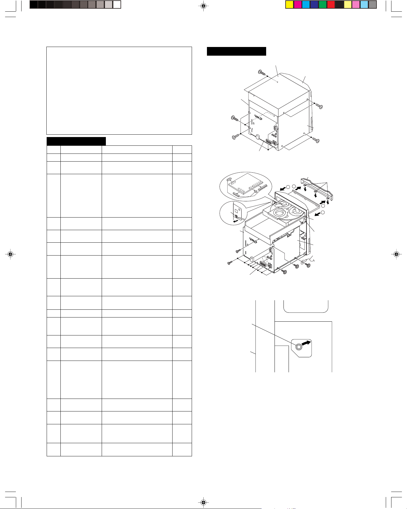
CD-E750DV
STEP
REMOVAL
1 Top Cabinet 1. Screw ...................... (A1) x4 6-1
2 Side Panel 1. Screw ...................... (B1) x8 6-1
(Left/Right)
3 DVD Player 1.
Unit/DVD Tray the disc tray, take out the
Cover CD tray cover, and close.
(Note 1)
2. Screw ...................... (C1) x1
3. Hook ........................ (C2) x3
4. Hook ........................ (C3) x2
5. Socket ..................... (C4) x4
4 DVS PWB 1. Screw ...................... (D1) x3 7-1
2. Socket ..................... (D2) x1 7-1
5 SURROUND 1. Screw ...................... (E1) x2 7-1
PWB 2. Socket ..................... (E2) x1 7-1
6 Rear Panel with 1. Screw .......................(F1) x9 6-2
Fan Motor 2. Socket ...................... (F2) x1 7-2
7 Main PWB 1. Screw ...................... (G1) x4 7-2
2. Socket ..................... (G2) x4 7-2, 7-3
3. Flat Cable ............... (G3) x1 7-2
4. Flat Wire .................. (G4) x1
8 Front Panel 1. Screw ...................... (H1) x1 7-2
2. Hook ........................ (H2) x2
3. Flat Wire .................. (H3) x1
9 Mic PWB 1. Screw ....................... (J1) x2 7-3
2. Tip Wire .................... (J2) x1
10
Headphones PWB
1. Screw ...................... (K1) x1 7-3
11 Display PWB 1. Knob ......................... (L1) x1 7-4
2. Screw ..................... (L2) x10
3. Flat Cable ................ (L3) x1
12 Tape Mechanism 1. Open the cassette holder. 7-4
2. Screw...................... (M1) x5
13 Turntable 1. Hook ........................ (N1) x2 7-5
2. Stabilizer Holder ..... (N2) x1
14 Loading Tray 1.
2. Push the loading tray 7-6
15 DVD Servo 1. Screw ...................... (Q1) x2 8-1
PWB (Note 2) 2. Flat Cable ............... (Q2) x1
16 DVD Mechanism 1. Hook........................ (R1) x2 8-2
2. Hook ........................ (R2) x2
17 Joint PWB 1. Screw ...................... (S1) x2 8-3
2. Hook ........................ (S2) x3
3. Socket ..................... (S3) x2
18 DVD Loading 1. Hook ......................... (T1) x6 8-4
Motor PWB
PROCEDURE
Turn on the power supply, open
Turn fully the lock lever in the
arrow direction.
backward to engage the claw
with the groove and remove
it in the direction of the
arrow. (P1) x6
FIGURE
6-2
6-3
(B1)x4
ø3x10mm
Rear
Panel
(B1)x2
ø3x10mm
Figure 6-1
2
(G1)x1
ø3x10mm
DVD Tray Cover
1
Lug Wire
(G1)x1
ø3x10mm
(F1)x1
ø3x10mm
(C2)x3
1
2
DVD Playe
Unit
(C3)x1
Main PWB
(C3)x1
Pull
Rear
Panel
(C1)x1
ø3x10mm
(F1)x8
ø3x10mm
DVD
SERVO PWB
(C4)x4
Fan Motor
Figure 6-2
Lock Lever
DVD Player Unit
(Bottom View)
Figure 6-3
Note 1: How to open the changer manually. (Fig. 6-3)
1. In this state, turn fully the lock lever in the arrow direction through
the hole on the loading tray bottom.
2. After that, push forward the Loading tray.
Note 2:
1. After removing the connector for the optical pickup from the
connector, wrap the conductive aluminium foil around the front end
of the connector so as to protect the optical pickup from electrostatic damage.
Note 3:
1. Be careful not to break the claw of the DVD mechanism.
2. When fining back the cam gear assembly, let it lock by front
movement.
A4 (pg 01-8) 7/9/03, 2:26 PM6
– 6 –
Page 7
(D1)x3
(P1)x3
3
(P1)x3
Loading Tray
1
2
ø3x10mm
S Video
PWB
Rear
Panel
(D2)x1
Main PWB
Display PWB
(L2)x10
ø3x10mm
Tape
Mechanism
Lug Wire
CD-E750DV
(L3)x1
Front Panel
(L1)x1
Open
(E1)x2
ø3x10mm
(H2)x1
Power PWB
Transformer
PWB
(G1)x2
ø3x10mm
(H3)x1
(G2)x1
(F2)x1
Figure 7-1
(G3)x1
Main PWB
(G2)x1
(H1)x1
ø3x10mm
(E2)x1
Surround
PWB
Front Panel
(G4)x1
Headphones
PWB
(H2)x1
(M1)x5
ø3x10mm
Cassette
Holder
Lug Wire
Figure 7-4
(N2)x1
Turntable
Loading
Tray
(N1)x2
Figure 7-2
(G2)x1
DVD Player Unit
Figure 7-5
Front Panel
Display PWB
(J2)x1
Tape
Mechanism
(J1)x2
ø3x10mm
ø3x10mm
(G2)x1
(K1)x1
Figure 7-3
Mic
PWB
Headphones
PWB
Figure 7-6
– 7 –
A4 (pg 01-8) 7/9/03, 2:26 PM7
Page 8
CD-E750DV
(T1) x 6
DVD Loading
Motor PWB
1 Woofer 1. Front Panel ............. (A1) x1 8-5
2. Screw ...................... (A2) x8 8-6
2 Tweeter 1. Screw ...................... (B1) x2 8-6
STEP
REMOVAL
PROCEDURE
FIGURE
CP-E750DV
DVD Servo
PWB
(Q2) x 1
Figure 8-4
(Q1) x 2
ø3 x 8mm
Figure 8-1
(R1) x 1
(S1) x 2
ø3 x 8mm
Joint PWB
DVD
Mechanism
(S2) x 3
Figure 8-2
(R1) x 1
Slide
Chassis
(R2) x 2
Loading Tray
Driver should
be pried away
from Speaker Box.
Woofer
(A1)x1
Speaker Box
Figure 8-5
(S3) x 2
Figure 8-3
A4 (pg 01-8) 7/9/03, 2:26 PM8
– 8 –
(A2)x4
ø4x12mm
(B1)x2
ø3x10mm
(A2)x4
ø4x12mm
Tweeter
Woofer
Speaker Box
Figure 8-6
Page 9
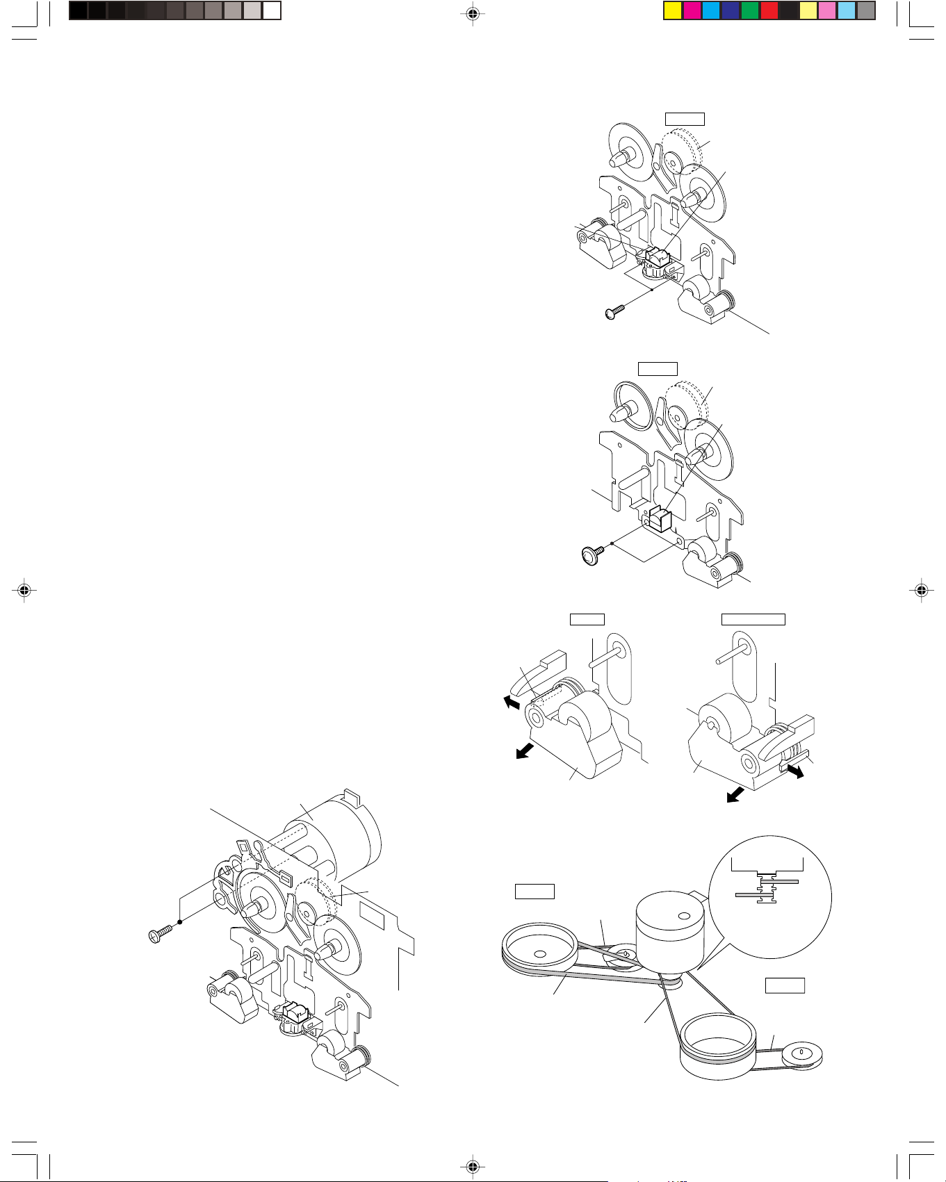
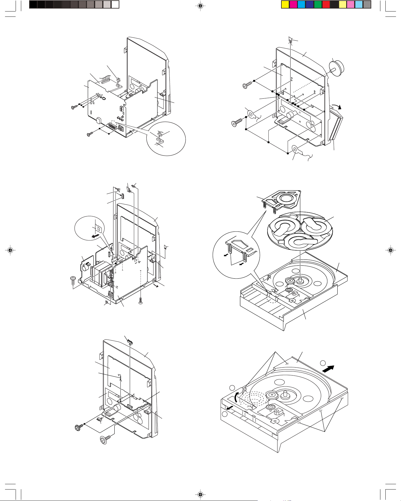
REMOVING AND REINSTALLING THE MAIN PARTS
TAPE MECHANISM SECTION
Perform steps 1 to 6 and 10 of the disassembly method to
remove the tape mechanism.
How to remove the record/playback and erase
heads (TAPE 2) (See Fig. 10-1)
1. When you remove the screws (A1) x 2 pcs., the recording/
playback head and three-dimensional head of the erasing
head can be removed.
How to remove the playback head (TAPE 1)
(See Fig. 10-2)
1. When you remove the screws (B1) x 2 pcs., the playback
head can be removed.
How to remove the pinch roller (TAPE 1/2)
(See Fig. 10-3)
1. Carefully bend the pinch roller pawl in the direction of the
arrow <A>, and remove the pinch roller (C1) x 1 pc., in the
direction of the arrow <B>.
Note:
When installing the pinch roller, pay attention to the spring
mounting position.
Erase Head
(A1)x2
Ø2x6mm
Figure 10-1
TAPE 1
TAPE 2
Clutch Ass'y
Record/Playback
Head
Clutch Ass'y
Playback
Head
CD-E750DV
How to remove the belt (TAPE 2)
(See Fig. 10-4)
1. Remove the main belt (D1) x 1 pc., from the tape motor side.
2. Remove the FF/REW belt (D2) x 1 pc.
How to remove the belt (TAPE 1)
(See Fig. 10-4)
1. Remove the main belt (E1) x 1 pc., from the tape motor side.
2. Remove the FF/REW belt (E2) x 1 pc.
How to remove the motor (See Fig. 10-5)
1. Remove the screw (F1) x 2 pc., to remove the tape motor.
Tape
Motor
Clutch Ass'y
(F1)x2
Ø2.6x5mm
Pinch
Roller
Pawl
<A>
Pull
<B>
TAPE 2
TAPE 2
Pinch Roller
(C1)x1
(B1)x2
Ø2x9mm
FF/REW
Belt
(D2)x1
Figure 10-2
Pinch Roller
(C1)x1
Figure 10-3
Tape
Motor
TAPE 1/TAPE 2
Pull
<B>
TAPE 2
Main Belt
(D1)x1
Tape
Motor
<A>
TAPE 1
Main Belt
(E1)x1
Pinch
Roller
Pawl
A4 (pg 9-14) 7/9/03, 2:26 PM9
– 9 –
Main Belt
(D1)x1
Main Belt
(E1)x1
Figure 10-4Figure 10-5
TAPE 1
FF/REW
Belt
(E2)x1
Page 10
CD-E750DV
ADJUSTMENT
MECHANISM SECTION
• Driving Force Check
Torque Meter Specified Value
Play: TW-2111 Tape 1: Over 80 g
• Torque Check
Torque Meter
Play: TW-2111 30 to 80 g.cm 30 to 80 g.cm
Fast forward: TW-2231 — 70 to 180 g.cm
Rewind: TW-2231 — 70 to 180 g.cm
• Tape Speed
Test Tape
Normal MTT-111 Variable 3,000 ± 30 Hz Speaker
speed Resistor in Terminal
Adjusting
motor. (Load
TAPE MECHANISM
Tape 2: Over 80 g
Tape 1
Point
Specified Value
Specified
Value
Tape 2
Instrument
Connection
resistance:
6 ohms)
• FM RF
Signal generator: 1kHz, 40 kHz dev., FM modulated
Test Stage
Frequency
Frequency
Display
FM Band — 87.50 MHz T301 (fL): *1
Coverage 1.3 V ± 0.1 V
FM RF 98.00 MHz 98.00 MHz L312 *2
(10-30 dB)
Setting/
Adjusting
Point
Instrument
Connection
*1. Input: Antenna Output: TP301
*2. Input: Antenna Output: Speaker terminal
• FM IF
Signal generator: 10.7 MHz, FM modulated
Test Stage
Frequency
Frequency
Display
Setting/
Adjusting
Point
IF 10.7 MHz 98.00 MHz T302 *1
(Turn the
core of transformer T302
fully counterclock wise)
Instrument
Connection
*1. Input: Antenna Output: TP301
MAIN PWB
Tape
Motor
Variable Resistor in motor
Figure 11-1
TUNER SECTION
fL: Low-range frequency
fH: High-range frequency
• AM IF/RF
Signal generator: 400 Hz, 30%, AM modulated
Test Stage
Frequency
Frequency
Display
AM IF 450kHz 1,602 kHz T351 *1
AM Band — 531 kHz (fL): T306 *2
Coverage 1.1 V ± 0.1 V
AM Tracking 990 kHz 990 kHz (fL): T303 *1
*1. Input: Antenna Output: TP302
*2. Input: Antenna Output: TP301
Setting/
Adjusting
Parts
Instrument
Connection
SO301
TERMINAL
FM ANTENNA
CNP301
ANTENNA
AM/FM LOOP
FM BAND
COVERAGE fL
R381
TP301
IC301
1
T303
AM TRACKING
fL
L312
T302
FM RF
T301
FM IF
T306
AM BAND
COVERAGE fL
T351
AM IF
Figure 11-2 ADJUSTMENT POINTS
R356
TP302
A4 (pg 9-14) 7/9/03, 2:26 PM10
– 10 –
Page 11
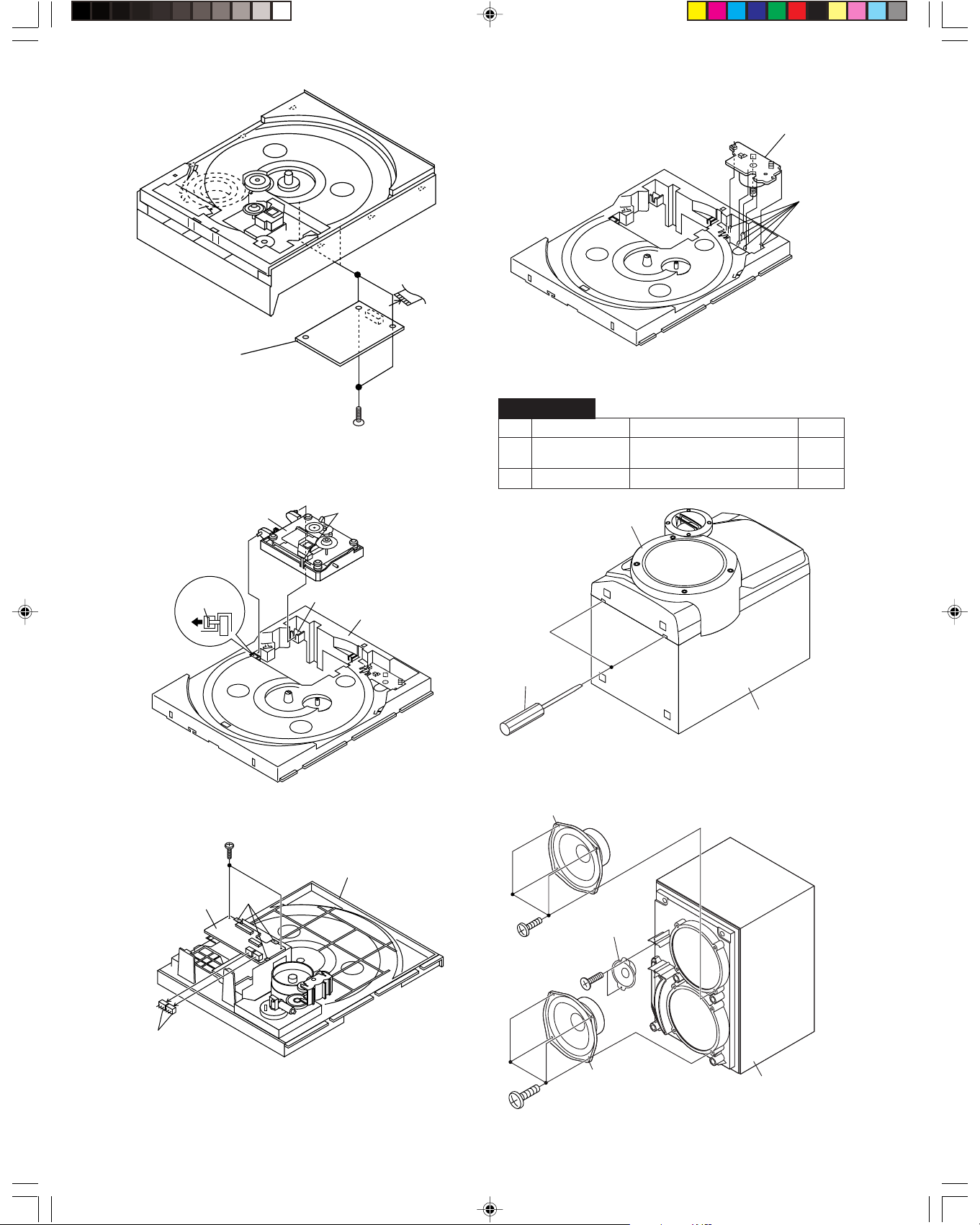
CD-E750DV
DVD/CD SECTION
• Adjustment
Since this DVD/CD system incorporates the following automatic adjustment functions, readjustment is not needed when replacing
the pickup. Therefore, different PWBs and pickups can be combined freely.
Each time a disc is changed, these adjustments are performed automatically. Therefore, playback of each disc can be performed
under optimum conditions.
DVD TEST MODE
DVD Test Mode Pressing down the DVD/CD button and X-BASS/DEMO button, press POWER button.
ROM Renewal Mode Pressing down the DVD/CD button and EQUALIZER button, press POWER button.
[DVD TEST MODE]
Test mode initial image plane
F0000000 *AD#####
<The "1" key of the remote controller is pushed.>
(* is a region number)
(##### is a program version)
The preparation date display of the program
10000000 ********
(Last updata)
The "Playback" key of the remote controller is pushed.
Model number display
10000001 *******#
(Model number)
The "Playback" key of the remote controller is pushed.
The version display of the program
10000002 ********
(Program ver.)
The "Playback" key of the remote controller is pushed.
Reagion number display
10000003 0000000*
(Region code:Binary display)
The "Reactivation" key of the remote controller is pushed.
Micro-code number display
10000004 ********
(Microcode ver.)
The "Playback" key of the remote controller is pushed.
The preparation date display of the servo program
10000005 ********
(Servo ver.)
(* is a model number) (# is a region number)
(* is a region number)
Micro-code is the thing of the process
program of the system integrated circuit.
To (1)
A4 (pg 9-14) 7/9/03, 2:26 PM11
The "Playback" key of the remote controller is pushed.
It is returned to the test mode initial image plane.
<The "2" key of the remote controller is pushed.>
Color bar display
20000001 00000000 (FIP)
The "Stop" key of the remote controller is pushed.
It is returned to the test mode initial image plane.
<The "3" key of the remote controller is pushed.>
Dynamic Test
30000000 00000000
– 11 –
There is no copy guard signal.
As for the symptom when it was
dubbed in the video tape recorder?
Page 12

CD-E750DV
From (1)
<The "1" key of the remote controller is pushed.>
DVD laser lights, the spindle motor
rotates and the pickup moves to the
outer periphery.
30000001 000000DD
<The "1" key of the remote controller is pushed.>
DVD laser off, CD laser on, spin kick,
sled outer periphery feed
ErrDisplay0 ErrDisplay1
30000001 000000CD
<The "1" key of the remote controller is pushed.>
Laser off, spin kick, sled outer periphery
feed
ErrDisplay0 ErrDisplay1
30000001 00000000
<The "1" key of the remote controller is pushed.>
The "stop" key of the remote controller is pushed.
It is returned to the Dynamic test.
Note: Not to face the light of the laser squarely,
caution!
<Disk is put, and the "2" key of the remote controller is pushed.>
*It is usually returned in power source off for the state.
STEP TEST
30000201 00000000
STEP TEST
30000202 00000000
STEP TEST
30000203 00000000
STEP TEST
30000204 00000000
STEP TEST
30000205 00000000
STEP TEST
DD000210 00000000
Focus on
The "PLAY" key input.
RF gain adjustment, Track on
The "PLAY" key input.
Focus gain adjustment
The "PLAY" key input.
Track gain adjustment
The "PLAY" key input.
Focus balance adjustment
The "PLAY" key input.
STEP TEST
3000E201 000000EE
When a disk is not in.
(In case of CD)
STEP TEST END
CD000210 ********
(******** is sub-Q.)
After TOC Reading,
Follow-up play condition
STEP TEST
DD000211 00000000
The "PLAY" key input.
STEP TEST END
DD000212 ********
(******** is the sector ID.)
The "Stop" key of the remote controller is pushed.
It is returned to the Dynamic test.
To (2)
A4 (pg 9-14) 7/9/03, 2:26 PM12
Focus balance of the layer 1,
follow-up play condition after focus gain adjustment
– 12 –
Page 13

From (2)
"3" Key input
Following playback, jump test mode
PLAY TEST
30000001 00000000
"Open/Close" Key input
CD-E750DV
Because a tray opens, adisk is published.
PLAY TEST
DD######*********
Error rate lever ver
1ber=5error
It is returned to the test mode initial image plane.
Spin offset adjustment mode
"TOP MENU" Key input
SPIN OFFSET
It becomes following play state.
(******** is a sector ID.)(###### is a error rate)
A test jump can be done by inputting the following key
from the remote controller.
Key Jump Key Jump
1-131
4 -102 6 102
7 -510 9 510
Clear -511 Enter 511
2 -765 Repeat 765
5 -766 A-B Repeat 766
8 -7000 Memory 7000
Before skipping. -15000 After skipping. 15000
>10 Layer Jump
The"Stop" key of the remote controller is pushed.
PLAY TEST
00000000 0000*****
(**** is a adjustment result.)
[DVD ROM RENEWAL MODE]
1. A DVD itself and a personal computer are articulated as
the right figure for. Software the renewal is started more.
2. Pressing down the DVD/CD button and EQUALIZER button,
press POWER button.
WRITE It is displayed.
3. Start a data transfer within 5 seconds -30 seconds after
you go into DVD ROM RENEWAL MODE.
4. AC code is removed after a data transfer is finished.
5. AC code is put again, and it is within DVD test mode,
and program version is confirmed.
Fixture for the
ROM renewal
Adapter cord
RS232C
Personal computer
(DOS)
RUNTK0808GEZZ
RCA PIN PLUG
RCA PIN JACK
QCNWK0001AWZZ
Unit
Molex 2pin conector
Figure 13
A4 (pg 9-14) 7/9/03, 2:26 PM13
– 13 –
Page 14

CD-E750DV
CD ERROR CODE DESCRIPTION
Error Explanation
01 When Pickup set inner position, inner switch cannot
detect 'ON' level for 10 secs.
When tray moves to Open/Close, Open/Close
10*
11* “CLAMP SW”, “DISC NO SW”, and “OPEN/CLOSE
30
switch can't detect “ON” level for 7 secs.
When disc table rotate to target position,
Clamp switch can't detect “ON” level for 7 secs.
When disc table set to Disc 1 position for 1st time,
SW” can't detect “ON” level for 14 secs.
Communication cannot be done between DVD and
System Microcomputer.
* 'CHECKING'
If Error is detected, 'CHECKING' will be displayed instead
of 'ER–CD**'. 'ER–CD**' display will only be displayed
when error had been detected for the 5th times.
Standard Specification of Stereo System Error
Message Display Contents
Error Contents
DVD/CD Pickup Mechanism 'ER–CD01' PU–IN SW
Error. Detection NG.
CD Charger 'ER-CD**' 10: Charger Error.
Mechanism Error. (*) 11: Initial Error.
DVD Communication 'ER-CD30' DVD
Error. COMMUNICATION
Focus Not Match/ 'NO DISC'
IL Time Over
TUNER PLL Unlock FM MHz PLL UNLOCK
DISPLAY
87.50
ERROR
Notes
+B PROTECTION is condition when irregular process
occur on power supply line.
BEFORE TRANSPORTING THE UNIT
The following process need to be taken after set tapering/
parts replacement.
1. Press the ON/STAND–BY button to enter stand–by
mode.
2. While pressing down the 3 button and the X–BASS/
DEMO button, press the ON/STAND–BY button until
“CLEAR AL” appears.
3. While pressing down the 4˜1 button and the
X–BASS/DEMO button, press the ON/STAND–BY button
until “WAIT” ––> “FINISHED” appears.
4. Unplug the AC cord and the unit is ready for
transporting.
Notes for handling the mechanism unit
Since the pickup semiconductor laser can easily damaged
by the static electricity, handle the mechanism unit with care.
To prevent damage by the static electricity during
transportation, the LD terminals are short-circuited at 2
points on the PWB. Unsolder them by a soldering iron after
completing the connection. When you return the mechanism
unit, solder the terminals again.
Soldering on the
mechanism PWB
(two points)
Flexible PWB
* 'CHECKING'
If Error is detected, 'CHECKING' will be displayed instead
of 'ER–CD**' display will only be displayed when error had
been detected for the 5th times.
Speaker abnormal detection and +B PROTECTION display
In case speaker abnormal detection or +B PROTECTION
had occured, it can be checked by pressing 'POWER',
'VIDEO' and 'X-BASS' key twice. Display will show “S**B**”.
S is referring to speaker abnormal detection and B is
referring to +B PROTECTION. ** is in hex value.
4X
DVD Motor PWB
Figure 14
A4 (pg 9-14) 7/11/03, 12:39 PM14
– 14 –
Page 15

NOTES ON SCHEMATIC DIAGRAM
• Resistor:
To differentiate the units of resistors, such symbol as K and
M are used: the symbol K means 1000 ohm and the symbol
M means 1000 kohm and the resistor without any symbol is
ohm-type resistor. Besides, the one with “Fusible” is a fuse
type.
• Capacitor:
To indicate the unit of capacitor, a symbol P is used: this
symbol P means pico-farad and the unit of the capacitor
without such a symbol is microfarad. As to electrolytic
capacitor, the expression “capacitance/withstand voltage”
is used.
(CH), (TH), (RH), (UJ): Temperature compensation
(ML): Mylar type
(P.P.): Polypropylene type
• Schematic diagram and Wiring Side of P.W.Board for this
model are subject to change for improvement without prior
notice.
CD-E750DV
• The indicated voltage in each section is the one measured
by Digital Multimeter between such a section and the chassis with no signal given.
1. In the tuner section,
indicates AM
indicates FM stereo
2. In the main section, a tape is being played back.
3. In the deck section, a tape is being played back.
( ) indicates the record state.
4. In the power section, a tape is being played back.
5. In the CD section, the CD is stopped.
• Parts marked with “ ” ( ) are important for
maintaining the safety of the set. Be sure to replace these
parts with specified ones for maintaining the safety and
performance of the set.
!
REF. NO
JOG701 JOG VOLUME ON—OFF
SW1 OPEN/CLOSE ON—OFF
SW2 CLAMP ON—OFF
SW3 DISC NUMBER ON—OFF
SW4 PICKUP IN ON—OFF
SW601 SPAN SELECTOR
SW701 ON/STAND-BY ON—OFF
SW702 MEMORY/SET ON—OFF
SW703 REC PAUSE ON—OFF
SW704 TUNING/TIME DOWN ON—OFF
SW705 TUNING/TIME UP ON—OFF
SW706
SW707
SW708 KARAOKE ON—OFF
SW709 ECHO ∨ ON—OFF
SW710 ECHO ∧ ON—OFF
TIMER/SLEEP
CLOCK
DESCRIPTION
POSITION
50 kHz/9 kHz—
100 kHz/10 kHz
ON—OFF
ON—OFF
TYPES OF TRANSISTOR AND LED
REF. NO DESCRIPTION POSITION
SW711
SW712 TUNER (BAND) ON—OFF
SW713 VIDEO/AUX ON—OFF
SW714 TAPE ON—OFF
SW715 STOP ON—OFF
SW716 PLAY ON—OFF
SW717 FAST FORWARD/PRESET UP ON—OFF
SW718 FAST REWIND/PRESET DOWN ON—OFF
SW719 REVERSE PLAY ON—OFF
SW720 REVERSE MODE ON—OFF
SW721 X-BASS/DEMO ON—OFF
SW722 EQUALIZER ON—OFF
SW723 OPEN/CLOSE ON—OFF
SW724 DISC SKIP ON—OFF
SW801 VOLTAGE SELECTOR
CD
ON—OFF
110 V—127 V—
220 V—230-240 V
FRONT
VIEW
E C B
(S) (G) (D)
(1) (2) (3)
KRA107 M
KRC102 M
KRC104 M
KTA1266 GR
KTA1271 Y
A4 (pg15-29) 7/9/03, 2:26 PM15
KTA1273 Y
KTA1274 Y KTA1046
KTC3194 Y
KTC3199 GR
KTC3200 GR
KTC3203 Y
B
(D)
FRONT
VIEW
(3)
E
TOP
VIEW
(G)
(1)
B C E
KTC2026 2SC2412 K
KRC104 S
KIA1504 Y
2SA1955 A
– 15 –
C
(S)
(2)
FRONT
VIEW
304VT2E1
A503BC2E
Page 16

CD-E750DV
O
0
K
P
3
4
O
D
V
U
D
HOLOGRAM
LASER UNIT
GND
HOLOGRAM
LASER UNIT
M1
SPINDLE
MOTOR
PICKUP IN
M2
SLED
MOTOR
OPEN/CLOSE
SW3
DISC NOMBR
M3
T/T UP DOWN
LOADING
MOTOR
ACTUATOR
–
+
–
+
–
+
–
+
(DVD)
OSC
–
+
–
+
–
+
–
+
–
+
(CD)
SW4
SW2
SW2
CAM
TO DISPLAY
FO+
TR–
TR+
FO–
LD
PD
VA
VB
VC
VD
Vref
Vcc
GND
Vcc
Vcc
VA
VB
VC
VE
VF
Vref
GND
LD
PD
M
M
M
UNIT
1
2
3
4
5
6
7
8
9
10
11
12
13
14
15
16
17
18
19
20
21
22
23
24
25
26
27
28
29
30
CP3202
LD_FWD
LD_RVS
DVD_FUNC
CAM_SW
DISC1_SW
UART_RX
DVD_BUSY
DVD_DI
DVD_DO
DVD_CLK
DVD_STB
D_GND
IC3301
TA1323F
TR+
FO+
TR-
FO-
+B9
+B9
Q3303
LDOI
46
MDI1
45
P1DI
52
P1CI
53
P1BI
54
P1AI
55
P2AI
58
P2BI
59
P2CI
60
P2DI
61
P2FP
63
P2FN
64
P2TP
2
P2TN
3
PITP
47
PITP
48
VrA
42
DFTN
22
SCB
13
SCL
14
SCD
15
VDD
8
RF SIGNAL PROCESSOR
51
LDP1
CD_LD
APCI
R-GAIN
ADJUST
F-GAIN
ADJUST
T-GAIN
ADJUST
BUS
DVD_LD
APC2
MDI2
LDO2
1,39,56,62
4
5
Q3302
FLGA
Q3301
LDP2
57
DPAC
RF RIPPLE
CREATION
EQ
DPDTE
CREATION
FE
CREATION
3BTE
CREATION
LEVEL
DETECT
DPBD
DPD1
IC3705
NJM2904M
OPE AMP.
+B8
5
6
8
7
9
4
3
C3207
2
–
1
+
3
5
+
7
–
6
+
14
–
SLN
+
13
–
SLP
+
12
–
SPN
+
11
–
SPP
+
17
–
FON
+
18
–
FOP
+
15
–
TRN
+
16
–
TRP
8
VCC
9
LDN
10
LDP
19,29,30
GND
BA5984FP
MOTOR DRIVER
OUTR
OUTL
+B10
+
–
SHIFT
LEVEL
+
–
SHIFT
LEVEL
+
–
SHIFT
LEVEL
SHIFT
+
–
SHIFT
LEVEL
IC3801
LOADING DRIVER
13
3
6
1
8
14
IC3201
74HC07AF
BUFFER AMP.
+
–
+
–
+
–
+
–
+B10
FWD,REV
12
MUTE
BIAS
OPOUT1
OPIN1(–)
OPIN1(+)
OPOUT2
OPIN2(–)
OPIN2(+)
OPOUT3
OPIN3(–)
OPIN3(+)
OPOUT4
OPIN4(–)
OPIN4(+)
4
5
2
9
7
–
+
–
+
–
+
–
+
1,28
DPD2
1211109
21
20
22
23
24
25
26
27
4
3
2
7
6
5
18,23,31,36
FE-GAIN
ADJUST
TE-GAIN
ADJUST
CONSTANT
VRCK
VRCK
+B9
RPO
RPZ
RFOP
RFON
EQF
EQB
TEB
DPDB
FEO
TEO
TIME
ADJUST
16 17
6
+B10
2
BR93L66F
26
25
30
29
44
43
33
35
21
20
19
LVL
VCKF
7
1
SLDRV
5
SPDRV
IC3507
EEPROM
FOD
TRD
3
6
5
4
7
FEI
TEI
LVL
RFRP
RPZI
RFOP
RFON
EOF
EOB
TEB
DPDC
SLDRV
SPDRV
FDD
TRD
SPV
FLGA
VRCK
SCB
SCL
SCD
/DFTN
+B10
5
42,3
IC3503
PST9129N
RESET
UART-RXD
KEY3
S/E_DI
S/E_DO
S/E_CK
FIP_CS
EECS
+B10
138 PVDD
ADC
150
FEI
151
TEI
152
LVL
153
RFRP
146
RFZI
142
RFCD
143
RFDVD
139
RFON
DAC IF
(PWM)
168
ANMON
167
EQBC
164
TEBC
166
DPDC
162
FMO
163
DMO
DAC
158
FOO
159
TRO
156
EXT_DA
37 FLGA
170 VRCK
174 SCB
173 SCL
172 SCD
169 /DFCT
+B10
1,11,26,40,62,76,86
VDD1
ID
DETECT
MEMORY CTL
IC3508
IX1761GE
TRACK BUFFER I/F
71 G_RESET
73 /RESET
67 CHOP
90 MUTE
100 EJ_SW
68 LD_SW
61 IN_SW
70,69 LD_FWD/REV
56 UART_RXD
97 KEY3
55 SUB/EEP_DIN
53 SUB/EEP_DOUT
57 SUB/EEP_CLK
S/E_CS
87
EECS
62
1,33,52,76,81
AVCC
93
6,15,24,38,47,59,79,104
103
AVSS
SERVO
DEQ
CONTROL
DIGITAL SERVO
DATA
SLICER
AVSS 149,154
PVSS 127
XVSS 9
DACVSS 3,8
VSS5 17,22,39,66
61,83,110
VSS3 105,122,171
45,51,64
ERROR
DETECT
RAM
(4.2KByte)
VCC
VSS
5 DAC VDD
144,160 AVDD
SLICE
LEVEL
GEN.
PLL
MICOM I/F
+B10
VDD2
777991 7880929394
+B10
SERV
MD0-7
MD0-7
46-53
72-65
5VBUS
N0O-N7O
HADR0-7 HDAT
MICR
SYNC
DEMOD
IC
TC9
PDC
SOSO_O
PSYCO
73
41
PD
IX
V
X
/
/SVAL_O
I
A4 (pg15-29) 7/9/03, 2:26 PM16
Figure 16 BLOCK DIAGRAM (1/4)
– 16 –
Page 17

CD-E750DV
+B10
+B10
DAC VDD
,160 AVDD
L
E
EL
.
L
ICOM I/F
MD0-7
7
VDD3 16,33,59
78,89,116
XVDD 12
SYNC DET.
DEMODULATION
IC3701
TC94A03F
SERVO ECC
/PDRQ
MD0-7
PDCK
46-53
72-65
5VBUS
N0O-N7O
HADR0-7 HDAT0-7 HRD HWR HAS HCS1 HCS2
MICROCOMPUTER
/PSYC
73 72 71
SDCK_O
/SVAL_O
SOSO_O
41 42 43 47 48 49
TIMING GEN.
HOST I/F
IC3504
IX1687GE
+B10
VDD5 54,74,95
OUTPUT I/F
PD0-7PDB
70
SDCK_I
/SVAL_I
PDRQI PDRQO
DRAM
60,62-65,67-69
PSYCI PDCKI PDCKO PSYCO
96-104
106-109,111-113
79-82,84-88
I/F
ECC
SD0_1,SD7_1
/SOSO_I
/HWR,FROM_CS,/RD 84,120,83
92,93
91
90,94
10
11
XO
/MCE 44
/MDR,/MWR
42,43
/MA 41
/MINT 45
/RST 40
52 53-60
PDI(0)-(7)/ERR_1
IPD I/F
OPD
I/F
PDON0O-N7O
PDON8O
VSS 10,25,29,39,44,50
61,63,75,85,100
AV-CS
HGA_INT
AV-INT
Z_STNBY
Z_RESET
/MA
SRV_CS
WAIT
/SRV_INT
VMUTE
S1_H
UART_CTL
UART_RXD
AMUTE2
ADAC_L
ADAC_CK
ADAC_DA
HGA_CS
A0-19 2-5,7-14,16-23
D0-15 34-37,39-46,48-51
/HWR,RAS 84,118
LCAS,CAS 86,116
DDAT0-15
DADR0-8
UCAS/LCAS
RAS
OE/WE
XI
FL3701
(22.5792MHz)
30-37
110,111,112
XTAL
EXTAL
38
119
26
30
64
65
66
117
92
31
109
108
58
56
88
112
111
110
60
77
78
2-5,7-10,31-34,36-39
16-19,22-26
28,29
14
27,13
A1-9
D0-15
/WA,RAS
LCAS,CAS
FL3501
(20MHz)
/WR,FRCS,/RD
IC3702
IX0447AW
4M EDO DRAM
/ERR_0
SDCK_O
/SOSO_O
/SVAL_O
SD0_O-SD7_O
/RD,/WR
+B10
Z_STNBY
Z_RESET
+B10
+B10+B10
+B10
FB3605
FB3604
D0-15
/WA,RAS
LCAS,CAS
FL_RESET
1,6,20
21,35,40
N.C
147
150
148
149
152-159
25-20
18,17
15,13
11,9-5
D0-15
30-27
A1-4
31,34
32
AVCS
39
WAIT
2
1
4
36
N.C
37
AVINT
134
N.C
145
143
N.C
122
124
160
N.C.
3,16,26,38,44,52,58,67
71,77,83,89,94,98,126
135,140,19,99
L3602
130
104
L3601
12,33,63,116,142
121
113
N.C
136-138
N.C
131
N.C
139
N.C
141
N.C
133
101,107,109,110
123,132
10,40,49,56,65,69
80,86,97,128,145,146
14,35,73,114,144
A1-9
A0-8
16-19,22-26
DQ1-16
2-4,7,8,31-34,36-39
WE,RAS
13,14
LCAS,UCAS
29,28
A1-19
A0-18
16-25,1-8,48
D0-15
DO1-16
29-36,38-45
WE,/CE,/OE/WR,FRCS,/RD
11,26,28
12 RP
151
IC6001
1,2,3
3.3
FLASH ROM
+B9
R3613
N.C
127
VCLKX2
PLL/CLOCK
HOST
I/F
I/F
I/F
IC3601
IX1720GE
7,8
65
I/F
ANALOG
VIDEO
ENCODER
I/F
TEST-SIO
I/F
VIDEO I/F
SDRAM
I/F
RAMDAT0-15
RAMADD0-11
91,88,85,82,79
76,74,70,88,72
75,78,81,84,87
90
13
14
15
16
VCC 1,6,20
VSS 21,35,40
VCC,VPP 37,13
BYTE 47
RY/BY 15
VSS 27,46
DVD-DSP
I/F
DVDREQ
DVDERR
DVDSTRB
DVDSOS
DVDVALID
DVDDAT0-7
HD0-15
HA0-3
HWR,HRD
HCS
HACK
HWID
HORD
HTYPE
HRDY
HIRQ
GENERAL
PURPOSE
GPIO
GPIS
GPSO
RESET/
STANDBY/
STATUS
STNBY
RESET
IDLE
DIGITAL
AUDIO
AIN
AOUT0-3
AMCLK
ALRCLK
ABCLK
S/PDIF
DVD DECODER
IC3502
IX0448AW
4M DRAM
IC3501
IX1689GE
X3601
27.0MHz
R3612
119
XO
GCLK
PLLCFG-I
PLLCFG-O
CVBS/G/Y
Y/R/V
C/B/U
CVBS/C
RSET
VREF
CQSYNC
ICEMODE
SCNENBL
TESTMODE
DIGITAL
VCLK
HSYNC
VSYNC
RAMME
RAMCAS
RAMRAS
RAMCS0,1
PCLK
RAMDOM
131,136,139,141
OE 27
WP 14
120
GCLK
112
125
129
FI
50,47,45
42,41,43
46,48,51
54,53,55
IC6004
+B10
+B10
N.C
2
62-60
57,59
R3552
R3555
102
105
106
103
108
111
100
117
115
118
Q3205
BUFF.
Q3203
BUFF.
Q3202
BUFF.
N.C
N.C
92
N.C
95
N.C
93
N.C
96
N.C
RAMCS0(FOR IC3602)
RAMCS1(FOR IC3603)
68
64
CP6001
2
D_1.8V
D_3.3V
+B7
Q5001,5004
Q5007,5010
CVBS
L.P.F
Q5002,5005
Q5008,5011
Y
L.P.F
Q5003,5006
Q5009,5012
C
L.P.F
R3603
R3604
+B10
RAMWE,RAMCAS
RAMRAS
PCLK
RAMDOM
RAMD0-15
RAMA0-11
IC3662
1.8V RGE
IC3661
3.3V RGE
15-17 WE,CAS,RAS
18 CS
35 CLK
14,36 LDOM/LDOU
DQ0-15
2,3,5,6,8,9,11,12,39
40,42,43,45,46,48,49
A0-11
21-24,27-32,20,19
A_5V
D_5V
M_GND
A_GND
D_GND
M_8V
J7002
S-VIDEO
IC501
TORX178A
DIGITAL OUT
IC3602/3603
IX0449AW
16M SDRAM
1,7,13,25,38,4434 CKE
4,10,26
41,47,50
CP3201
A_5V
D_5V
M_GND
A_GND
D_GND
M_8V
V_8V
SO7001
VIDEO OUT
+B10
VSS
+B10
A4 (pg15-29) 7/9/03, 2:26 PM17
Figure 17 BLOCK DIAGRAM (2/4)
– 17 –
Page 18

CD-E750DV
A4 (pg15-29) 7/9/03, 2:26 PM18
Figure 18 BLOCK DIAGRAM (3/4)
– 18 –
Page 19

CD-E750DV
A4 (pg15-29) 7/9/03, 2:26 PM19
Figure 19 BLOCK DIAGRAM (4/4)
– 19 –
Page 20

CD-E750DV
C
6
5
O
R3906
15K
R3905
8. 2K
TP3807
TP3809
TP3810
TP3811
IN_SW
C3302
1
C3303
C3304
C3305
C3301
1
1
1
R3303
2. 2K
1
ONLY OP
R3304
100M
Q3301
KTA1504Y
TP3341
LD_RVS
LD_FWD
R3310
4. 7K
R3907
R3345
TEB
TEB
32
RFS
1. 6
31
VccR
30
RFOp
29
RFOn
28
RPP
27
RPB
26
RPO
25
RPZ
24
NC
23
VccS
22
DFTN
21
FEO
20
TEO
19
LVL
18
VccP
17
WCKF
VRCK
16
2. 3
VRCK
6. 8K
R3705
4
HL
5
0
ONLY OP
100/6. 3
C3331
C3333
DVD
1000P
Q3307
C3332
ONLY OP
C3329
0.1
C3330
47/6. 3
0
ASLCO
C3324
0. 1
C3325
4700P
TP3331
C3326
4700P
RFRP
TP3332
RPZ
C3327
0. 1
DFCT
FE
TE
TP3333
LVL
C3328
0. 1
1. 5
C3323
0. 1
C3322
0. 01
C3321
47/6. 3
2. 2K
R3706
0. 01
C3704
SLDRV
R3834
8. 2K
2
3
1
0. 1
C3806
IC3802
TC7W53FU
7
6
8
CHOP
1000P
Q3701
KRC104S
MUTE
KRC1045
TP_RF
TP_GND
TP_FE
TP_TE
DVD_L
Q3702
KRC104S
R3707
C3705
220P
C3706
220P
L3701
1uH
L3702
C3718
R3713
00
0. 0082
R3722
ONLY OP
C3719
100M
0. 1
R3723
100M
R3724
100K
6800P
C3711
0. 1
10/16
C3710
00
C3707
47/6. 3
1uH
RPZ
C3709
220P
R3708
12K
FE
12K
TE
12K
LVL
12K
RFRP
R3712
FOD
TRD
C3708
0. 1
R3714
SLDRV
SPDRV
TEB
TP3712
TP3701
DPDB
EQB
EQF
DFCT
VRCK
SCD
SCL
SCB
8. 2K
C3712
C3716
C3717
4700P
0. 1
47K
C3723
C3724
C3713
R3709
R3710
R3711
220P
0. 1
0. 1
C3714
47/6. 3
0. 01
C373
0. 01
C3730
0. 1
0. 1
C3715
R372
00
ONLY OP
R3767
100M
220P
C3728
C3734
560P
18K
105K
R3717
R3715
1000P
C3731
C3729
4700P
R3727
330
R3728
330
R3729
39K
R3730
C3721
0. 015
27K
R3731
C3722
0. 015
27K
R3732
10K
R3733
10K
ONLY OP
R3734
C3725
10K
R3735
0. 1
C3726
10K
R3736
0. 1
C3727
10K
0. 1
R3725
R3716
1K
180
R3718
150
R3719
150
R3720
150
C3732
0. 1
C3733
0. 1
FB3301
R3821
R3822
1OuH
470
R3320
C3317
L3302
0. 1
10uH
C3315
47/6. 3
2. 2/50
C3311
10K
EQF
EQB
R3317
41
40
43
44
42
VrA
EQF
EQB
TCC1
RFDC
1. 6
1. 5
2. 5
1. 5
4. 7
3. 3
1. 6
1. 9
1. 2
Vdd
Vrfil
VrD
MD12
DPAC
789
5
6
C3310
C3313
1000P
47/6. 3
C3701
0. 01
C3702
82P
R3829
10K
22K
22K
R3825
1. 7
1. 7
1. 7
1. 7
1. 7
2
543
6
IN1
IN1
IN2
IN2
OPOUT1
IN3
IN3
IN4
IN4
OPOUT4
23
24
25
26
27
0
1. 7
1. 7
1. 7
1. 7
C3805
220P
10K
22K
R3826
R3824
33K
47K
R3830
39
GND2
0
10
C3314
1. 9
DPBD
1000P
0
1
LD-FWD
LD-RVS
28
0
38
NC
3. 8
DPD1
11
C3316
8
VCC
1
SPDRV
1000P
R3701
12
C3318
2
22K
37
NC
3. 8
DPD2
7
1000P
R3702
DPDB
353433
36
FEB
Vcc2
DPDB
0
4. 7
1. 6
4. 7
1. 5
0
2. 3
1. 6
0. 9
1. 7
4. 7
3. 2
1. 7
1. 7
0
4. 7
0
0
0
SCL
SCD
SCB
13
14
15
0. 1
C3320
SCL
SCB
SCD
5
6
GND
3
4
R3704
22K
C3703
82P
10K
10K
R3703
TRD
FOD
R3318
R3346
R3314
47
47
C3307
100/6. 3
C3306
0. 01
Q3302
2SA1955A
TP3342
R3343
1
0
0
R3908
C3802
0. 01
R3311
3. 3M
TP3343
C3803
10/16
R3344
1
R3340
R3336
00
2. 0
00
2. 0
3. 7
3. 7
D3301
DAP202K
31
TP3344
00
R3339
2. 0
3. 7
14
13
SLP
SLN
TRP
TRN
16
15
3. 7
TR+
TR-
3. 7
3. 7
R3319
47
47
C3312
C3319
47/6. 3
0. 01
Q3303
2SA1955A
R3316
3. 3M
2. 0
2. 0
46
48
45
47
LD01
MD11
P1TP
P1TN
49
P1FN (A)
0
4. 7
50
P1FP (B)
51
4. 7
LDP1
52
0. 2
P1DI
53
P1CI
2. 0
54
0
P1BI (B)
55
2. 0
P1AI (A)
56
0
GNDR
57
4. 7
LDP2
58
P2AI (A)
2. 0
59
P2BI (B)
2. 0
60
P2CI (C)
2. 0
61
2. 0
P2DI (D)
62
0
GNDS
63
2. 0
P2FP (B)
P2FN (A)
0
11
SPIN
FOP
18
0
FO+
0
10
LD
GND
19
Q3801
KRC104S
GND
123
0. 2
0
9
LD
BIAS
20
1. 2
R3817
P2TP (C)
C3308
47/6. 3
8. 0
8
VCC
MUTE
21
3. 2
C3804
100P
1K
P2TN (D)
NJM2904M
0
30
29
0
4. 7
LD02
4
C3309
0. 01
IC3705
1. 7
7
OPOUT2
OPOUT3
22
1. 7
64
3. 7
12
SPIN
FON
17
3. 7
FO-
DVD SERVO PWB-C (1/3)
A
B
CS3301
FW2
W2835RC
C
D
TP3304
50
TR+
TP3303
49
FO+
TP3302
48
TR-
TP3301
47
FO-
TP3305
46
TP3306
45
TP3307
44
43
TP3309
42
TP3310
41
TP3311
40
39
TP3312
TP3313
38
TP3314
37
TP3315
36
TP3316
35
TP3317
34
33
TP3318
TP3319
32
TP3320
31
30
TP3321
29
TP3322
TP3323
28
TP3324
27
TP3325
26
25
TP3326
TP3327
24
TP3328
23
TP3329
22
21
TP3330
20
NC
19
NC
18
TP3804
17
TP3805
16
15
ONLY 5H. 5U
TP3820
14
TP3802
13
TP3821
12
TP3822
11
10
ONLY 5H. 5U
9
8
7
6
5
4
3
2
1
E
CNS5
TO
JOINT PWB
P35 9-A
F
G
ONLY OP
H
• NOTES ON SCHEMATIC DIAGRAM can be found on page 15.
1
A4 (pg15-29) 7/9/03, 2:26 PM20
23456
Figure 20 SCHEMATIC DIAGRAM (1/16)
– 20 –
Page 21

CD-E750DV
7
0
10/16
4. 6
4. 6
DAT11
DAT10
2. 5
2. 5
33
8
0
0
DDAT4
DDAT5
DDAT3
99
BD4
BD3
0
NC
34
3. 0
DAT9
DAT8
2. 5
OE
LCAS
JCAS
31
292827
30
32
9
DDAT6
RASA8NCA7AOA6A1A5A2A4A3
11
13
14
10
12
1. 2
4. 7
4. 7
WE
RAS
DDAT7
0. 1
C3750
DDAT1
DDAT0
DDAT2
95
96
98
97
BD1
BD2
BD0
VDD5
0
0
0. 6
4. 7
4. 7
4. 7
3. 3
TEST1
NC
FLGB
FLGA
36
38
35
37
TP3711
ADR8
ADR7
ADR6
0
0
0
0
24
26
25
16
17
15
0
1. 7
1. 7
DADR1
DADR0
LCAS
UCAS
WE
0000000000
R3781
R3782
R3783
94
93
92
/BWE
/BCAS
/BCASL
4. 7
4. 7
4. 7
4. 7
3. 3
0
/RST
/MA
VSS3
41
39
40
1000P
C3751
/MA
/SRV_RST
ADR4
ADR5
0
0
21
23
22
VSS
C3752
0. 1
VCC
20
19
18
0
4. 7
DADR2
DADR3
C3753
0. 1
RAS
OE
R3785
R3784
3. 3
91
89
90
/BOE
VDD3
0
/BRAS
88
DADR8
BA8
3. 0
4. 7
3. 3
/MRD
42
/RD
3. 3
4. 6
4. 6
2. 3
4. 6
3. 3
4. 6
0. 9
/MWR
43
/WR
DADR7
87
BA7
0
86
DADR6
BA6
0
85
DADR5
BA5
0
84
DADR4
BA4
0
83
VSS5
0
82
DADR3
BA3
0
81
DADR2
BA2
0
80
DADR1
BA1
0
79
DADR0
0
BA0
78
VDD3
C3756
0. 1
77
TESM4
0
76
DIGI
0
75
TESM3
0
C3757
0. 1
74
VDD5
73
SDCK_I
PDCK
72
/PDRQ
/SVAL_I
71
SOSO_I
/PSYC
70
/ERR_I
4. 6
PD8
69
SD7_I
PD7
0
68
SD6_I
PD6
0
67
SD5_I
PD5
0
66
VSS3
0
65
SD4_I
0
PD4
64
SD3_I
0
PD3
63
SD2_I
PD2
0
62
SD1_I
PD1
0
61
VSS5
0
60
SD0_I
PD0
0
59
VDD3
0. 1
58
VMCK
0
C3759
TP3713
57
0
SMCK
TP3714
56
NC
55
C3758
NC
0. 1
54
VDD5
53
MD7
MD7
0
52
MD6
MD6
0
51
MD5
0
MD5
50
MD4
0
MD4
49
MD3
0
MD3
48
MD2
0. 1
MD2
47
MD1
MD1
0
46
MD0
MD0
0
45
/MINT
44
P22 1-C
TO DVD SERVO PWB (2/3)
P22 1-D
TO DVD SERVO PWB (2/3)
/SRV_INT
/SRV_CS
DDAT12
109
BD12
2. 5
0
MON1
24
TP3703
DDAT11
108
BD11
2. 5
0
MON2
25
TP3704
R3752
DAT13
DAT15
DAT12
DAT14
2. 5
2. 5
2. 5
2. 5
0
40
36
393837
D16D1D15D2D14D3D13D4D12D5D11D6D10D7D9D8NCNCLCASNCUCASWEOE
VSS
VCC
2
543
1
0
0
0
0. 6
4. 7
DDAT1
DDAT0
DDAT2
DDAT3
DDAT8
DDAT9
DDAT7
TP3707
105
VSS3
0
0
MON5
104
BD8
2. 5
0
MON6
TP3708
TP3709
103
BD7
1. 2
0
MON7
302928
DDAT6
102
BD6
0
0
MON8
31
TP3710
DDAT10
107
BD10
2. 5
0
MON3
26
TP3705
106
BD9
2. 7
1. 7
MON4
27
TP3706
0
4. 7
DDAT5
101
BD5
0
1. 5
MON9
32
2. 5
35
34
VSS
VCC
7
6
1. 2
DDAT4
100
1. 2
3. 3
VDD3
33
TP_DATA
TP_GND2
TP_CLK
ONLY OP
R3739
R37410R3743
4. 7k
R3737
C3718
R3713
00
0. 0082
ONLY OP
C3737
0. 1
R3722
ONLY OP
C3719
100M
0. 1
133
LPFN
R3723
100M
134
LPFO
R3724
100K
6800P
135
105K
C3721
0. 015
C3722
0. 015
ONLY OP
C3725
0. 1
C3726
0. 1
C3727
0. 1
R3716
180
ONLY OP
C3728
R3717
C3729
4700P
R3718
150
R3719
150
R3720
150
R3767
100M
220P
18K
C3732
C3733
C3730
0. 1
C3734
560P
R3727
R3728
R3729
R3730
R3731
R3732
10K
R3733
R3734
R3735
R3736
R3725
0. 1
0. 1
C3735
R3726
330
39K
27K
27K
10K
10K
10K
10K
0. 01
C3731
330
1K
PVREF
136
VCOREF
137
VCOF
138
PVDD
139
RFOn
140
TESM9
141
TEST2
142
RFCD
143
RFDVD
144
AVDD
145
RFCT
146
RFZI
00
TEZI
147
148
AWIN
149
AVSS
150
FEI
151
TEI
152
LVL
153
RFRP
154
AVSS
155
TESM10
1000P
156
EXTAD
157
VREF
158
FOO
159
TRO
160
AVDD
161
AWCTL
162
FMO
163
DMO
164
TEBC
165
NC (FEBC)
166
DPDC
167
EQBC
168
ANMON
169
/DFCT
170
VRCK
171
VSS3
172
SCD
173
SCL
174
SCB
175
FGIN
176
ASLCP
C3711
0. 1
7
. 3
C3714
47/6. 3
0. 1
C3715
C3713
0. 01
R3708
12K
R3709
12K
12K
R3710
12K
R3711
C3716
220P
R3715
8. 2K
R3712
C3717
4700P
C3712
0. 1
47K
R3714
C3723
12
0. 1
C3724
0. 1
VRCK
SCD
SCL
SCB
1. 5k
R3740
0. 1
1. 6
C3739
131
PDOP2
10K
R3745
R3746
33K
47K
100K
47K
R3744
R3742
0. 1
0. 1
0. 01
C3740
C3741
127
130
128
129
PESP
PVSS
PDOP1
PDON1
0
1. 6
1. 6
1. 6
00
33K
R3738
C3738
1. 6
132
PDON2
2. 9
1. 6
1. 6
0. 6
3. 3
1. 5
3. 3
1. 5
1. 5
3. 3
1. 6
1. 6
1. 0
0
1. 6
1. 6
1. 6
1. 6
0
1. 6
0
1. 6
1. 6
1. 6
3. 3
1. 6
1. 6
1. 6
1. 6
1. 6
1. 6
1. 5
1. 5
2. 4
1. 5
0
0
0
3. 3
0
ASLCN
1
0
ASLCO
2
ASLCO
0
1. 6
DACVDD
DVR
RO
DACVSS
3
5
4
6
C3742
0. 1
126
PESV
1. 6
1. 6
LO
7
R3747
C3745
C3743
0. 1
0. 1
0
00
R3749
R3752
150K
330K
R3750
R3753
119
TESM6
0
3. 3
TESM1
14
C3746
118
TESM5
0
3. 3
TESM2
15
0. 1
R3756
117
PLCK
0
3. 3
VDD3
16
C3734
0. 1
10
DDAT15
DDAT14
DDAT13
111
112
113
116
VDD3
3. 3
17
0
VSS3
R3757
R3758
114
115
NC
NC
3. 3
1. 6
VPFC
TESTO
19
18
1K
R3759
10K
C3748
0. 01
10K
20
BD15
2. 5
0
VLPFI
R3760
C3749
110
BD14
BD13
VSS5
0
2. 5
2. 5
0
0
1. 2
VSS3
VLPFO
MONO
21
23
22
TP3702
1K
0. 01
00
33K
R3748
R3751
121
123
CFC1
0. 8
1. 5
XI
10
0. 1
122
VSS3
0
1. 5
XO
11
R3754
1M
R3755
470
FL3701
C0001GEZZ
TESM8
3. 3
XVDD
12
120
TESM7
0
TESMO
13
124
CFC2
1. 5
0
XVSS
9
C3744
0
125
PPW
1. 6
0
DACVSS
8
7
A4 (pg15-29) 7/9/03, 2:26 PM21
P22 1-H,1-E
TO DVD SERVO PWB (2/3)
8 9 10 11 12
Figure 21 SCHEMATIC DIAGRAM (2/16)
– 21 –
Page 22

CD-E750DV
3
0
A
B
C
D
E
F
G
LVL
TE
RFRP
P21 12-C
TO DVD SERVO PWB (1/3)
P21 12-F
TO DVD SERVO PWB (1/3)
P21 12-H
TO DVD SERVO PWB (1/3)
4700p
C3524
P21 12-H
TO DVD SERVO PWB (1/3)
R3523 47K
ONLY OP
R3563
R3553 0
0
IC3503
PST9125N
/SRV_CS
5
1
A17
48
A16
A15
1
A16
CAS
AVCS
FRCS
47
A14
2
/BYTE
A15
2
RAS
R3564
R3565
15K
R3531
67
CHOP
1. 5
0
VSS
24
R3533 10K
/ERR_I
4. 7
4. 7
52
PDI [8]
4. 7
2. 3
DVDREQ
4. 7
0
PDCKO
PDRQO
PSYCO
0
3. 3
0
PDO [8]
0
0
PDO [7]
PDO [6]
0
PDO [5]
0
PDO [4]
0
PDO [3]
0
PDO [2]
0
PDO [1]
0
0
PDO [0]
0
3. 3
3. 3
HCS2
24
0
3. 3
/SRV_CS
D11
0. 2
34
DQ12
DQ5
7
1. 5
D4
/MA
66
/MA
3. 3
0
A20
25
A20
51
VDD2
PSYCI
PDRQI
PDCKI
VDD2
HWAIT
VSS
25
1. 5
0. 3
R3534
65
Z_RESET
3. 3
3. 1
0. 2
26
HGA_INT
VSS
VSS
VDD1
VSS
VSS
HINT
VDD1
R3560
D10
33
DQ11
DQ6
8
D5
3. 3
HGA_INT
10K
10K
R3535
0
64
Z_STNBY
3. 3
SUB/EEP CLK
0
SUB/EEP Din
1. 4
SUB/EEP Dout
0. 6
TRAY_REQ
27
10K
R3538
50
49
48
47
46
45
44
43
42
41
40
39
38
37
36
35
34
33
32
31
30
29
28
27
26
3. 3
10K
D9
0. 2
0. 2
32
DQ10
DQ7
9
0. 3
0. 3
D6
EECS
10K
R3537
0
63
62
EEP-CS
PLAY-MODE
UART-CTL
UART-RXD
UART-TXD
3. 3
1. 5
1. 5
0. 2
1. 5
0. 2
0. 2
0. 3
0. 3
0. 3
1. 5
1. 5
1. 5
1. 5
0. 2
3. 3
0
STBY_REQ
H/P CTL
28
29
0. 2
ONLY OP
R3539
0
4. 7
R3568
100
R3569
100
C3527 0. 01
R3581 10K
D8
31
DQ9
DQ8
10
D7
IN_SW
4. 7K
R3540
3. 3
61
IN_SW
IN_SW
VCC
0
0
0
0
VCC
SRV_
INT
AV_INT
30
3. 3
AV_INT
10K
R3542 10K
/ERR_O
SD7_O
SD6_O
SD5_O
SD4_O
SD3_O
SD2_O
SD1_O
SD0_O
HGA_INT
C3526
47/6.3
3. 0
30
NC
NC
11
C3515
0. 01
VSS
D15
D14
D13
D12
VSS
D11
D10
D9
D8
D7
D6
D5
D4
VSS
D3
D2
D1
D0
R/C
R3556
1K
/SOSO_I
SDCK_I
R3566 10K
C3528
0. 01
LCAS
3. 3
29
LCAS
NC
12
3. 3
60
0
59
0. 1
58
57
56
55
54
53
52
51
50
49
48
47
46
45
44
43
42
41
40
39
38
37
36
35
34
33
R3554 10K
32
0. 2
31
R3541 1K
ONLY OP
/SVAL_I
SDCK_O
/SVAL_O
/SOSO_O
ONLY OP
CAS
0
28
UCAS
WE
13
3. 1
/WR
R3543
10K
3. 3
R3546 100K
S/E_CK
R3547 1K
S/E_DI
S/E_DO
D15
D14
D13
D12
D11
D10
D9
D8
D7
D6
D5
D4
D3
D2
D1
D0
3. 3
/SRV_INT
R3545 1K
R3562
100M
27
OE
RAS
14
RAS
HGA_CS
R3544
4. 7K
A9
3. 1
26
A8
NC
15
ONLY OP
3. 3
WAIT
A8A7A6
0. 3
25
A7
A0
161718
1. 6
A1
0. 1
C3503
C502
100/6. 3
0. 3
24
A6
A1A2A3
0. 3
A2
C3505
UART-RXD
C3504
3. 0
23
A5
0. 3
A3
C3603
C3601
4
CLK S/E_CK
DIN
5
S/E_DO
100/6. 3
EECS
3
OCNT
6
BR93L66F
S/E_DI CS
A4
A3
A2
A1
/WR
AVCS
/RD
AV_INT
WAIT
2
VCC
GND
7
IC3507
E2PROM
C3602
100/6. 3
0. 1
D15
D14
D13
D12
D11
D10
C3605
0. 1
D9
D8
C3606
0. 1
D7
D6
D5
D4
D3
D2
D1
D0
C3607
0. 1
C3608
0. 1
C3609
0. 1
1
C3519
NC
0. 01
NC
8
3. 3
3. 3
0
0
R3557
2. 2K
R3558
4. 7K
Q3502
KTA1504Y
VPP_CTL
C3604
0. 1
0
1
HORD
2
HWID
3
VDDP
4
HTYPE
5
HD-15
6
HD-14
7
HD-13
8
HD-12
9
HD-11
10
GNDP
11
HD-10
12
VDDC
13
HD-9
14
GNDC
15
HD-8
16
VDDP
17
HD-7
18
HD-6
19
VDD_LVL_SHFT
20
HD-5
21
HD-4
22
HD-3
23
HD-2
24
HD-1
25
HD-0
26
VDDP
27
HA-3
28
HA-2
29
HA-1
30
HA-0
31
HWR
32
HCS
33
VDDC
34
HRD
35
GNDC
36
HRDY
37
HIRQ
38
VDDP
39
HACK
40
GNDP
0
160
1. 6
1. 6
1. 6
1. 7
41
0. 1
SD7_O
159
IDLE
DVDDAT7
0
3. 3
3. 3
0
1. 6
0. 2
0. 1
0. 2
0
1. 6
1. 8
0. 2
0
0. 2
3. 3
2. 8
1. 6
1. 6
1. 6
1. 6
0
3. 3
0. 3
0. 3
0. 3
3. 3
3. 3
0. 9
0
0
3. 3
0. 1
RAMADD4
RAMADD3
42
RAMA4
RAMA3
SD5_O
SD6_O
158
157
DVDDAT6
DVDDAT5
0
0
3. 3
0. 1
3. 3
RAMADD5
VDDP
434445
C3610
0. 1
RAMA5
C3640
0. 1
SD4_O
SD3_O
155
156
DVDDAT3
DVDDAT4
0
0
0. 1
0. 1
RAMADD2
RAMADD6
46
RAMA2
RAMA6
0. 7
0
50
VSSO
VCC
1
3. 3
1. 7
RAMD15
49
I/O15
I/00
2
RAMD0
SD2_O
154
DVDDAT2
0
0. 1
RAMADD1
47
RAMA1
0. 1
RAMD14
48
3
1. 7
RAMD1
I/O14
I/01
SD1_O
153
DVDDAT1
0
0. 1
RAMADD7
48
RAMA7
1. 2
RAMD13
0
46
47
I/O13
VSSO
VSS0
I/02
5
4
0
0. 5
RAMD2
SD0_O
152
DVDAT0
0
0
GNDP
49
2. 4
0. 5
TP3604
RAMD12
45
I/O12
I/03
6
RAMD3
DVDREQ
TP3605
151
DVDREQ
3. 3
0. 1
RAMADD0
50
RAMA0
0. 3
RAMD11
3. 3
43
44
I/O11
VCCO
VCC
I/04
8
7
2. 6
3. 3
RAMD4
SDCK_O
TP3606
150
DVDSTRB
1. 6
0
RAMADD8
51
C3611
0. 1
RAMA8
0. 5
RAMD10
42
I/O10
I/05
9
1. 4
RAMD5
/SVAL_O
149
DVDVALID
3. 3
3. 3
VDDP
52
/ERR_O
/SOSO_O
TP3608
TP3607
148
147
DVDERR
DVDSOS
0
3. 3
0. 1
1. 7
RAMADD9
RAMDD10
5354555657
RAMA10
RAMA9
1. 7
1. 7
RAMD8
RAMD9
3. 3
0
41
39
38
40
I/08
I/09
VSSO
VCCO
VCC0
VSS0
I/07
I/06
11
13
10
12
0
0. 6
5. 6
3. 3
RAMD6
RAMD7
146
GNDP
0
0
RAMADD11
RAMA11
0
37
NC
DOML
14
0
RAMDQM
145
GPSI
0
0
GNDP
RAMDQM
0
36
DOMU
WE
151617
3. 3
RAMWE
1. 7
3. 3
144
GNDC
0
0
RAMCS0
C
RAMCSO
35
CLK
CAS
3. 3
RAMCAS
3. 3
34
CKE
RAS
RAMRAS
TP3503
Q3503
KRC104S
0. 1
TP3501
0. 1
TP3515
ONLY OP
DVDREQ
R3567
100M
A5
0
0. 3
21
22
A4
VSS
C3516
0. 01
VCC
20
19
0. 3
3. 3
A4
MUTE
DVD_L
R3514
R3518
R3517
1K
1K
WAIT
FIP_CS
/WR
LCAS
R3516 10K
TP3509
TP3510
TP3511
R3508
R3509
R3510
R3512
R3511
R3501 1K
R3502 10K
R3503 10K
R3504 10K
1
C3523
0. 01
TP3508
C3508
0. 1
3. 3
TP3513
10
10
15K
10
10K
0
3. 3
0
R3513
4. 7K
91
MODE_SW
92
WAIT
93
AVCC
94
VREF
95
KEY1
96
KEY2
97
KEY3
98
LVL
99
TE
100
EJ_SW
101
RFRP
102
RESERVE (SRV)
103
AVSS
104
VSS
105
STANDBY
106
TRAY_ACK
107
WOBBLE
108
S1_H
109
VMUTE
110
ADAC_CK
111
ADAC_L
112
ADAC_DA
113
MD_0
114
MD_1
115
MD_2
116
CAS
117
SRV_CS
118
RAS
119
AV_CS
120
FROM_CS
C3501
0. 1
76
VDD1
77
BUF5O [B]
78
BUF5I [B]
79
BUF5O [A]
80
BUF5I [A]
81
GPO [3]
82
GPO [2]
83
GPO [1]
84
GPO [0]
85
VSS
86
VDD1
87
LI [1]
88
LI [2]
89
BUFO [C]
90
BUFI [C]
91
BUFO [B]
92
BUFI [B]
93
BUFO [A]
94
BUFI [A]
95
TEST0
96
TEST1
97
TEST2
98
NC
99
MRST
100
VSS
3. 3
3. 3
88
86
87
89
90
85
84
/LWR
LCAS
MUTE
/HWR
DVD_L
/E_CAS
AMUTE2
0. 3
0. 3
0. 3
0. 3
3. 3
3. 3
3. 3
3. 3
3. 3
0. 9
0
3. 9
0. 9
0
0
0
0
0
3. 3
0
0
3. 3
3. 3
0
3. 3
3. 3
0
0. 3
0. 3
0. 3
1. 6
VSS
A1
A2
A4
VCC
A0
A3
7
6
2
5
3
4
1
0
3. 3
A1
A0
A3
A2
MD1
MD2
MD0
MD3
0
74
71
70
69
75
73
72
NC
NC
VSS
5VBUS [0]
5VBUS [2]
5VBUS [3]
5VBUS [1]
4. 6
0
2. 1
1. 4
0. 5
0. 5
0
1. 5
0
0
3. 3
3. 0
3. 0
3. 0
3. 0
0
0
0
0
3. 0
0. 3
0. 3
0. 3
0. 3
1. 6
VDD1
HADR0
HADR2
HADR3
HADR1
HADR4
HADR5
7
5
1
2
3
4
6
0
C3511
R3506
5. 6K
10K
43
0. 1
ONLY OP
C3509
47/6. 3
C3510
R3505
3. 3K
R3507
3. 3K
ADAC_CK
ADAC_L
ADAC_DA
C3522
47/6. 3
TP3504
TP3505
TP3506
TP3507
TP3514
R3515
150K
D3501
DAP202K
0. 1
3. 3K
C3512
3. 3
A1
A3
A4
A2
A0
A5A6A7
C3517
0. 01
D11
D4
D14
D12
D3
D13
D15
D6
D7
D5
41
36
40
46
45
D15
VSS
A12
A13
3
4
A13
A14
38
35
39
42
43
44
D7
A11
5
A12
37
D5
D6
D14
A9
A10
7
6
A11
A10
D3
D4
D11
D12
D13
VDD
/WE
/WP
VPP
/RP
A8
NC
NC
8
9
11
10
14
12
13
ONLY OP
100M
R3550
A2
A9
/WR
ONLY OP
R355I
/RD
D10
D9
D1
D2
D8
DO
27
29
31
28
30
33
34
32
D1
D0
D2
D9
D8
/OE
D10
RY/BY
15
VSS
A7
A17
A6
A5
A18
A4
21
20
19
22
18
16
17
A18
A7A6A5
A4
A19
A8
1K
/RD
83
/RD
0
0. 3
A5A6A7
8
MD4
68
5VBUS [4]
0. 5
3. 0
HADR6
8
FRCS
26
/CE
A3
A2
23
A3
/AS
R3519 1K
81
82
/AC
VCC
0
0
3. 0
0. 1
9
10
A6A5A4
A7
MD5
MD6
66
67
5VBUS [6]
5VBUS [5]
2. 3
1. 5
0. 1
0
VSS
HADR7
9
10
0. 01
C3525
A1
25
A0
A1
24
A2
ONLY OP
C3507
0. 1
10K
R3520
80
0
0. 1
A8
11
A8
MD7
65
5VBUS [7]
1. 8
3. 3
VDD1
11
C3515
FL3501
C0207GE
R3522
10
R3521
100M
ONLY OP
R3524
10K
10K
10K
R3528
R3525
0. 1
C3506
70
71
74
79
75
76
73
69
NMI
0. 3
0. 4
A13
17
A13
SD1_I
59
PDI [1]
0
/RESET
3. 3
0. 3
A14
18
A14
SD2_I
58
PDI [2]
0
72
/WDGOVF
3. 3
0. 2
A15
19
A15
SD3_I
57
PDI [3]
0
G_RESET
0
(S-ID)LD-RVS
0
(SEARCH)LD-FWD
0
0
0
3. 3
A16
A18
A17
21
22
20
A16
A18
A17
SD4_I
SD5_I
SD6_I
56
54
55
PDI [6]
PDI [5]
PDI [4]
0
0
0
68
LD_SW
0
0
A19
23
A19
SD6_I
53
PDI [7]
0
VSS
0
3. 0
A9
12
A9
64
VDD2
4. 7
78
EXTAL
0. 2
0. 3
A10
13
A10
C3521
0. 01
C3520
0. 01
63
VSS
0
77
XTAL
2. 8
A11
14
A11
62
VDD1
3. 3
VCC
/STBY
3. 3
0. 3
0. 2
0
3. 0
A12
VSS
15
16
A12
SD0_I
61
60
VSS
PDI [0]
0
0
0
3. 3
0
0
0. 2
0. 2
0. 2
1. 5
1. 6
3. 3
0
3. 3
3. 3
HWR
HRD
HCS1
0
16
40
1
HDAT4
A12
VSS
VCC
3. 3
HDAT5
17
A13
D15
0
39
DQ16
DQ1
2
0. 2
D0D1D2
HAS
HDAT7
HDAT6
21
22
23
20
19
18
ONLY OP
100M
R3559
/RD
A15
A14
HGA_CS
/WR
/AS
D14
D13
D12
0
0
1. 5
1. 5
35
38
36
37
VSS
DQ15
DQ14
DQ13
VCC
DQ2
DQ3
DQ4
3
4
5
6
1. 6
1. 5
1. 5
3. 3
D3
HDAT0
HDAT2
HDAT3
HDAT1
14
15
12
13
A11
A10
A8
A9
0. 01
H
• NOTES ON SCHEMATIC DIAGRAM can be found on page 15.
1
A4 (pg15-29) 7/9/03, 2:27 PM22
23456
Figure 22 SCHEMATIC DIAGRAM (3/16)
– 22 –
Page 23

CD-E750DV
DVDAT0
0
2
4
0
0
5
GNDP
SD0
O
49
152
DVD SERVO PWB-C (2/3)
C3632
AMCLK
AOUT0
ALRCLK
145
146
GPSI
GNDP
0
0
0
0
GNDP
RAMADD11
RAMA11
RAMDQM
0
0
37
36
NC
DOMU
WE
DOML
14
151617
0
3. 3
RAMWE
RAMDQM
1. 7
353433
CLK
CAS
3. 3
RAMCAS
144
GNDC
0
0
RAMCS0
C3612
0. 1
RAMCSO
3. 3
CKE
RAS
3. 3
RAMRAS
C3635
142
143
GPSO
0
3. 3
VDDP
585960
0. 1
1. 8
32
NC
CS
19
18
3. 3
0. 2
RAMCS0
0. 1
R3621
VDDC
1. 7
3. 3
RAMCS1
RAMCS1
0. 1
RAMA8
RAMA9
31
A8
A9
A11 (BS)
A10 (+)
20
1. 5
RAMA10
RAMA11
ABCLK
C3634
141
ABCLK
1. 6
3. 3
RAMRAS
RAMRAS
0. 1
RAMA7
30
A7
A0
21
0. 5
RAMA0
0. 1
140
VDDP
3. 3
3. 3
RAMCAS
61
RAMCAS
0. 1
RAMA6
29
A6
A1
22
0. 1
RAMA1
R3620
139
ALRCLK
1. 6
3. 3
RAMWE
62
C3613
RAMWE
0. 1
RAMA5
28
A5
A2
23
0. 1
RAMA2
220
220
R3617
220
220
R3618
R3619
138
137
136
AOUT-1
AOUT-2
AOUT-0
0
0
0
0
0
1. 7
VDDC
GNDP
RAMDQM
63
646566
R3670
0. 1
RAMDQM
0. 1
RAMA4
0
27
26
A4
VSS
C3641
VCC
A3
25
24
0. 1
3. 3
RAMA3
_
/SVAL_O
/ERR_O
/SOSO_O
SDCK_O
DVDREQ
TP3606
TP3608
TP3607
TP3605
TP3604
151
149
148
150
147
DVDERR
DVDSOS
DVDREQ
DVDSTRB
DVDVALI D
0
3. 3
3. 3
1. 6
3. 3
3. 3
0. 1
0. 1
0
1. 7
VDDP
RAMADD8
RAMADD9
RAMDD10
RAMADD0
51
50
5354555657
52
C3611
0. 1
RAMA10
RAMA9
RAMA8
RAMA0
.
RAMD12
45
I/O12
I/03
6
.
RAMD3
3. 3
44
VCCO
VCC
7
3. 3
0. 3
RAMD11
43
8
2. 6
RAMD4
0. 5
1. 7
1. 7
RAMD10
RAMD8
RAMD9
3. 3
0
41
39
38
42
40
I/08
I/09
I/O11
I/O10
VSSO
VCCO
VCC0
VSS0
I/07
I/04
I/05
I/06
9
11
13
10
12
0
1. 4
0. 6
5. 6
3. 3
RAMD6
RAMD5
RAMD7
0. 1
C3631
47/6. 3
L3602
150
R3615
132
GNDP-A2
0
131
AMCLK
1. 6
130
VDDP-A2
3. 3
47uH
128
129
GNDP
0
TESTMODE
0
127
VCLKx2
1. 6
126
VDDP
3. 3
FB3606
125
SCNENBL
0
0. 1
390
R3633
R3616
134
135
133
GPI0
VDDP
S/PDIF
2. 8
3. 3
1. 6
3. 3
3. 3
RAMDAT3
RAMDAT12
0. 3
0
0. 5
1. 5
1. 7
3. 3
3. 3
0
C3643
GNDP
69
0
VDDP
GNDC
RAMDAT9
72
RAMD9
3. 3
737475
0. 7
0
50
VSSO
VCC
1
1. 7
RAMD15
49
I/015
I/00
2
RAMD0
0. 1
48
3
1. 6
RAMDAT6
RAMD6
RAMD14
I/014I/01
RAMD1
RAMDAT5
RAMDAT10
76
1. 5
C3616
0. 1
RAMD10
RAMD5
2. 4
1. 2
RAMD12
RAMD13
0
47
46
45
I/013
I/012
VSSO
VSSO
I/03
I/02
5
4
6
0
0. 5
0. 5
RAMD3
RAMD2
RAMDAT7
71
70
C3615
0. 1
RAMD7
0. 1
1. 7
VDDP
PCLK
RAMDAT8
68
67
100
C3614
0. 1
RAMD8
PLCK
0. 1
C0353AF
124
123
GNDA
RESET
0
3. 3
0
3. 3
0
0
0
2. 2
0. 3
0. 3
0
0. 3
VDD_LVL_SHFT
1. 6
0. 7
1. 6
0. 2
0. 5
1. 2
VDDP
RAMDAT11
777879
3. 3
2. 4
RAMD11
0. 3
RAMD11
3. 3
44
43
I/011
VCCO
I/04
VCCO
8
7
2. 7
3. 3
RAMD4
122
STNBY
3. 3
PLLCFG-0
1. 5
1. 7
0
PLLCFG-1
0
ICEMODE
0. 6
GND-DACS
GND-DACP
1. 2
GND-DACB
0. 9
0. 3
VDD-DAC
CVBS/G/Y
GND-DACD
0. 3
0
3. 3
3. 6
3. 6
1. 6
RAMDAT0
RAMDAT15
3. 3
RAMDAT1
RAMDAT14
0
RAMDAT2
RAMDAT13
RAMDAT4
0. 6
RAMD4
0. 5
RAMD10
42
I/010
I/05
9
1. 4
RAMD5
1. 7
121
VDDA
GCLK
GCLK1
VDDC
GNDC
0
VREF
RSET
C/B/U
Y/R/V
CVBS/C
COSYNC
VDDP
GNDP
1. 6
HSYNC
VDDP
VSYNC
VCLK
VDDP
GNDP
VDDP
GNDP
80
0
C3617
100/6. 3
1. 7
RAMD9
0
41
40
I/09
VSSO
VSS0
I/06
11
10
0
0. 7
RAMD6
C3630
XO
AIN
1. 7
0. 5
0. 1
FI
RAMD8
39
I/08
I/07
12
RAMD7
C3629
100/6. 3
FB3605
C0353AF
120
119
118
117
116
115
114
113
112
111
110
109
108
107
106
105
104
103
102
101
100
99
98
97
96
95
94
93
92
91
90
89
88
87
86
85
84
83
82
81
C3618
0. 1
3. 3
38
VCCO
VCCO
13
3. 3
1. 5
1. 5
0. 5
2. 5
0
37
NC
DOML
14
0
RAMDQM
C3619
RAMDQM
0
36
DOMU
WE
15
3. 3
RAMWE
C3623
0. 1
1. 8
3. 3
0. 1
353433
CLK
CAS
16
RAMCAS
3. 3
CKE
RAS
17
3. 3
RAMRAS
C3628
47/6. 3
C3622
0. 1
0
NC
18
3. 3
RAMCS1
R3612
R3602
RAMD0
RAMD15
RAMD1
RAMD14
RAMD2
RAMD13
C3621
0. 1
RAMD3
RAMD12
C3620
100/6. 3
0. 1
CS
0. 2
680K
R3613
10K
0. 1
RAMA9
32
A9
A11 (BS)
19
0. 5
RAMA11
150
R3603
RAMA8
31
A8
A10 (+)
20
RAMA10
X3601
FB3604
C0353AF
R3605
56
FB3601
C0353AF
0. 1
RAMA7
30
A7
A0
21
1. 5
RAMA0
100M
C0002AW
R3604
0. 1
0. 1
C3627
C3626
390
RAMA6
29
A6
A1A5A2
22
RAMA1
10P
10P
L3601
0. 1
0. 1
C3625
0. 1
RAMA5
28
23
RAMA2
TP3502
10K
0. 1
L3202
ONLY OP
0
R3672
0. 1
ONLY OP
C3671
100/6. 3
D3601
1SS133
ONLY AT100. AT10
10K
R3206
C0353AF
D3662 D3661
C3207
1000P
D3602
1SS133
1
2
3
4
5
6
7
10
11
12
TERMINAL
A_5V
D_5V
M_GND
A_GND
D_GND
M_8V
V_8V
DISPLAY
1
LD+(SERCH)
2
LD-(S-ID)
3
D_GND
4
DVD_STB
5
UART RX
6
DVD_BUSY
7
DVD_DO
8
DVD_DI
9
DVD_CLK
TUN_FNC
CLAMP SW
CD/DI_SW
CP3202
M890M
CP3201
M890G
CNS701
P27 12-C,D
FROM DISPLAY PWB
P34 2~5-B
TO DVD SERVO PWB (3/3)
1
2
3
4
P24 1-C
5
CNS601
6
FROM MAIN PWB
7
R3201
000
R3202
R3215
1K
ONLY AT10, AT100
TC74HC07AF
R3220
470
IC3662
TA4802F
(2. 0V)
2
IC3661
2
C3665
R3211
C3666
000
R3204 100
R3228 100
R3203 100
R3208 100
R3209 100
ONLY 5H, 5U
R3205
R3212
1. 8K
470
R3218
0
9
8
10
C3206
GND
7
5
6
R3221
000
R3214
1. 8K
L3201
C0353AF
ONLY 5H, 5U
13
0. 1
C3673 47/6. 3
1
0. 01
C3667 47/6. 3
C3668
0. 01
UART-RXD
R3216
ONLY OP
R3606
100M
R3607
56
R3608
56
ONLY OP
R3609
100M
C3610
56
ONLY OP
R3611
100M
R3227
C3624
47/6. 3
680
Q3205
KTA1504Y
47uH
C3201
R3225
R3226
680
680
Q3203
Q3202
KTA1504Y
KTA1504Y
C3203
0. 1
0. 1
C3204
0. 1
22K
ONLY AT10, AT100
R3217
0
131211
14
VCC
IC3201
ONLY 5H, 5U, 5W
234
1
R3219
ONLY AT10, AT100
R3213
R3207
2. 2K
C3205 47/6. 3
R3210
2. 2K
SPDIF_O
R3661 10
R3662 10
R3663 10
ADAC_CK
ADAC_DA
ADAC_L
AMCLK
ABCLK
AOUT0
ALRCLK
D2. 5V
0. 1
C3662
C3664
C3661
47/6. 3
IX0445AW
(NJM2391DL/3. 3)
3
0. 1
C3663
47/6. 3
100/6. 3
C3670
0. 01
C3669
0. 1
27
24
0. 1
RAMA4
A4
A3
RAMA3
C0353AF
C3644
FB3603
0. 1
C3646
100/6. 3
0
26
VSS
VCC
25
3. 3
C3674
C3672
0. 01
7
A4 (pg15-29) 7/9/03, 2:27 PM23
8 9 10 11 12
Figure 23 SCHEMATIC DIAGRAM (4/16)
– 23 –
Page 24

CD-E750DV
A
B
C
D
MAIN PWB-A (1/3)
P34 3-F
CP6001
TO DVD PWB
P28 1-D~G
CP3201
P23 12-G
TO DVD PWB
VDD
VREF
ROUT
RBASS
RTRE
RIN
RSELO
CLK
24
23
22
21
20
19
18
17
R4
16
R3
15
R2
14
R1
13
DI
1
CE
2
VSS
3
LOUT
4
LBASS
5
LTRE
6
LIN
7
LSELO
8
L4
9
L3
10
L2
11
L1
12
INTERFACE
TUNER
CCB
AUX
DECK
CD
E
F
G
H
• NOTES ON SCHEMATIC DIAGRAM can be found on page 15.
1
A4 (pg15-29) 7/9/03, 2:27 PM24
23456
Figure 24 SCHEMATIC DIAGRAM (5/16)
– 24 –
Page 25

TO MIC PWB
P33 12-D,E
CNPK1
CD-E750DV
CNSK1
KOK OUT(L)
KOK IN(L)
A_GND
A_+10V
KOK IN(R)
KOK OUT(R)
D_GND
CLK
KOK LATCH
MIC IN
DI
P31 9,10-H
TO TUNER SCETION
FFC701
20
P26 1-E,F
CNP701A
TO DISPLAY SECTION
AGND (AUDIO PRO)
A+10V
TAPE_A_GND
TUN_FUNC
M_GND
7
8 9 10 11 12
D_GND
+B_PROTECT
P28 1-D~G
M_+13V
SW_5V
SP_DET
SP_RLY
1
Figure 25 SCHEMATIC DIAGRAM (6/16)
– 25 –
A4 (pg15-29) 7/9/03, 2:27 PM25
Page 26

CD-E750DV
10
A
LED A PWB-A4
NP
F
F
P21
P20
P19
P16
P13
P12
P15
35
P14
343332
P11
31
P18
45
43
42
44
P17
40
393837
41
36
P10
P09
30
29
NXNXNXNXNXNXNX
P07
P08
282726
G08
G09
P06
P03
P05
24
22
23
25
P04
21
20
17
19
16
18
G07
P02
P01
14
15
11
13
12
LED B PWB-A5
B
81
83
868788
84
85
82
S11
80
S12
79
VLOAD
78
S13
S14
77
76
S15
75
S16
74
DIST3/S17
DIST2/S18
73
DIST1/S19
72
DIST0/S20
C
D
71
70
S21
69
DIST
68
67
66
65
UART RX
64
63
ILU_LED1
62
61
60
59
LD M–
LD M+
58
57
MO_SPEED
56
KARAOKE LATCH
55
MIC SW
54
O/C_SW
53
52
T1 RUN
51
T2 RUN
50
S6S7S8
S9
S10
VDD
RLY
AC_RLY
TIMER LED
SP_
47
46
49
48
454443
S5
T_MOTOR
89
S3
S4
IC701
IX0598AW
T_SOL_A
T_SOL_B
42
90
S2
SMUTE
41
91
S1
VSS
40
93
92
G8
G9
SP DET
REMOCON
38
39
94
G7
CD CLAMP SW
37
E
F
G
H
CNP701B
P25 12-F,G
TO MAIN PWB
FFC701
20
1
TUN_FUNC
SPAN
MIC IN
+B_PROTECT
D_GND
S_MUTE
T_T1/T2
REC/PLAY
T_BIAS
A+10V
M_+13V
SW_5V
SP_DET
SP_RLY
–20dB
CE
DO
CLK
DI
TAPE MECHANISM
PWB-E
• NOTES ON SCHEMATIC DIAGRAM can be found on page 15.
1
A4 (pg15-29) 7/9/03, 2:27 PM26
23456
Figure 26 SCHEMATIC DIAGRAM (7/16)
– 26 –
Page 27

16
DISPLAY PWB-A2
CD-E750DV
G08
G09
G05
G07
G04
P03
P02
15
G06
P01
14
13
12
G03
9
8
7
11
10
NP
F
G01
G02
4
5
2
6
3
1
FOR DVD ROM WRITER ONLY
91
89
S3
IC701
IX0598AW
T_SOL_B
42
90
S2
SMUTE
41
S1
VSS
40
93
92
G8
G9
SP DET
REMOCON
383736
39
94
G7
CD CLAMP SW
95
G6
P_IN
969798
G5
G4
TUN FUNC
DVD_WRITE
DISC_NO SW/
T2_PLAY SW/
FPA/FPB SW
AVREF
AVDD
34
35
99
G2
G3
–20dBATT
T–BIAS
T_T1/T2
REC/PLAY
SPAN
RESET
XOUT
VPP/IC
XT2
DVD_STB
DVD CLK
DVD DI
DVD DO
AVSS
DSA DATA
PROTECT
LVL_DET
32
33
100
G1
1
VDD
2
3
4
5
6
7
8
9
10
11
12
XIN
13
14
15
16
VDD
CLK
17
18
DI
19
DO
20
CE
21
22
23
24
25
26
27
28
29
30
31
CP3202
P23 12-C
TO DVD PWB
CNP802
P29 7-F,G
TO POWER PWB
7
A4 (pg15-29) 7/9/03, 2:27 PM27
8 9 10 11 12
Figure 27 SCHEMATIC DIAGRAM (8/16)
– 27 –
Page 28

CD-E750DV
A
B
C
D
E
F
G
P24 1-C,B P25 9,10-H
H
• NOTES ON SCHEMATIC DIAGRAM can be found on page 15.
1
A4 (pg15-29) 7/9/03, 2:27 PM28
23456
Figure 28 SCHEMATIC DIAGRAM (9/16)
– 28 –
Page 29

MAIN PWB-A1 (3/3)
HEAD PHONE PWB – A3
SURROUND SPK PWB – D
CD-E750DV
SURROUND_SP_Lch
SURROUND_SP_Rch
SURROUND_SP_Lch_GND
SURROUND_SP_Rch_GND
FW701
P27 11,12 - E
FROM DISPLAY PWB
7
A4 (pg15-29) 7/9/03, 2:27 PM29
POWER PWB-B2POWER PWB-B1
8 9 10 11 12
Figure 29 SCHEMATIC DIAGRAM (10/16)
– 29 –
Page 30

CD-E750DV
0
U
A
B
C
AM LOOP
ANTENA
MAIN PWB-A1 (2/3)
AM BAND
COVERAGE fL
AM TRACKING
AM ANTENA
AM OSC
1
FM BAND
D
FM ANTENA
TREMINAL
FM IF
COVERAGE
fL
1
2
3
AM IF
3
2
E
OSC BUFFER
F
IC3
LC72
PLL (T
G
H
• NOTES ON SCHEMATIC DIAGRAM can be found on page 15.
1
A4 (pg 30-48) 7/9/03, 2:28 PM30
23456
Figure 30 SCHEMATIC DIAGRAM (11/16)
– 30 –
Page 31

CD-E750DV
AM IF
1
3
2
IC302
LC72131
PLL (TUNER)
7
A4 (pg 30-48) 7/9/03, 2:28 PM31
P 25 12 – C, D
TO MAIN SECTION
8 9 10 11 12
Figure 31 SCHEMATIC DIAGRAM (12/16)
– 31 –
Page 32

CD-E750DV
A
B
C
D
E
F
G
H
• NOTES ON SCHEMATIC DIAGRAM can be found on page 15.
1
A4 (pg 30-48) 7/9/03, 2:28 PM32
23456
Figure 32 SCHEMATIC DIAGRAM (13/16)
– 32 –
Page 33

MIC PWB-G
CD-E750DV
7
A4 (pg 30-48) 7/9/03, 2:28 PM33
CNSK1
P 25 9, 10 – A
FROM MAIN PWB
8 9 10 11 12
Figure 33 SCHEMATIC DIAGRAM (14/16)
– 33 –
Page 34

CD-E750DV
DVD SERVO PWB-C (3/3)
P 23 12 – D
TO DVD SERVO PWB (2/3)
CNSK602
P 24 1 – A
FROM MAIN PWB
CNSV1
P 25 11, 12 – B
FROM DVS PWB
A
B
C
D
E
F
G
H
• NOTES ON SCHEMATIC DIAGRAM can be found on page 15.
1
A4 (pg 30-48) 7/9/03, 2:28 PM34
23456
Figure 34 SCHEMATIC DIAGRAM (15/16)
– 34 –
Page 35

CD-E750DV
FW2
SL+
SL+
SL–
SL–
GND
1
28
CNS5
341159
CNP2
CNS1A
IN_SW
SP–
SP–
SP+
6347
1
345626
345612
SP+
DISC1_SW
CAM_SW
LD/EJ_SW
GND
LD–
LD+
LD+
15 19
12
10
741253
74153
16
14 17
26
264 153
CNP3
CNS2
LD–
BI2
CS3301
20
TO
DVD SERVO PWB
P20 1-E
VB
VFVAPDVEVR
GND
2421 22
FO–
TR–
TR+
GND
VCC
VC
V/2 LDVB
VOSC
VD
GND
GND
29
272526
3018312332 3533
VCPDVR
36283837
GND
V/2 VAVCC
LD
41 43403942
44 48
GND
45 49471346
FO+
50
JOINT
PWB-J
CNS4
–
+
29
28
VF
VB
2526 20
27 2123
VA
VE
PD
GND
2230
24
VC
VR
M
17
14
19
15
LD
GND
VCC
V/2
GND
FW1
VD
VOSC
1018 16
1213
11
95
VA
VB
GND
VR
VC
PD
43
82
76
LD
V/2
GND
GND
VCC
TR+
FO+
1
TR–
FO–
SW3
SW1
CAM
DISC1
M3
CNS1B
CN4
+
123456
123456
–
–
SW2
OPEN/CLOSE
+
MM
M2
SLED
MOTOR
SW4
PICKUP IN
M1
SPINDLE
MOTOR
DVD MOTOR PWB-I
MOTOR
LOADING
T/T UP/DOWN
FLEXBLE
DVD LOADING
MOTOR PWB-H
VB
VFVAPDVEVR
GND
2526 20
27 2123
29
28
CN2
CN1
30 18 101214
PWB
GND
VA
VF
VB
30
28
26
25 2027
29
GND
VCC
VC
19
2230 10
24
23 21 1727 2025 1626
LD
VC
VRVEPD
VCC
GND
2123
24
19 15
V/2LDVB
VOSC
VD
GND
17
18 16
15
151924
GND
VD
VOSC
V/2
16
17
DVD
PICKUP
UNIT
GND
VCPDVR
14
1213
11
1129
1328
VA
VC
GND
VB
14 12 1018
13
11
GND
GND
V/2 VAVCC
LD
43
82
76
95
8
597
6
2
LD
VCC
V/2
GND
VR
PD
GND
TR–
FO–
43221
8
795
2
6
1
12234
FO+
TR+
FO–
TR–
TR+
FO+
• NOTES ON SCHEMATIC DIAGRAM can be found on page 15.
7
A4 (pg 30-48) 7/9/03, 2:28 PM35
8 9 10 11 12
Figure 35 WIRING SIDE OF P.W.BOARD (16/16)
– 35 –
 Loading...