

Page 1
CD-DV600W
SERVICE MANUAL
No. XXXXXXXXXXXXX
DVD MINI SYSTEM
M
TE
S
Y
S
I
N
I
M
D
V
D
00
6
CD-DV
L
E
V
E
L
C
I
M
2
IC
M
1
X
A
M
N
I
A
S
W
3A
03
A
G
C
M
R
R
NTSC/PAL
M
CHAPTER 1. GENERAL DESCRIPTION
[1] Specifications ................................................. 1-1
[2] Names of parts............................................... 1-2
CHAPTER 2. ADJUSTMENTS
[1] Mechanism section ........................................ 2-1
[2] Tuner section ................................................. 2-1
[3] DVD/CD section ............................................. 2-2
[4] TEST Mode .................................................... 2-3
[5] CD Changer mechanism section ................. 2-10
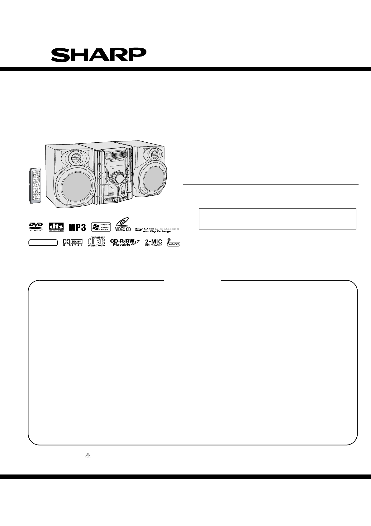
MODEL
CD-DV600W
CD-DV600W DVD Mini System consisting of CD-DV600W
and CP-DV600 (speaker system).
• In the interests of user-safety the set should be restored to its
original condition and only parts identical to those specified be
used.
CONTENTS
CHAPTER 5. CIRCUIT DESCRIPTION
[1] Notes on schematic diagram .........................5-1
[2] Types of transistor and LED ..........................5-1
[3] Waveforms of DVD circuit.............................. 5-2
[4] Voltage...........................................................5-3
CHAPTER 6. CIRCUIT SCHEMATICS AND PARTS
LAYOUT
[1] Schematic diagram........................................6-1
[2] Wiring side of PWB......................................6-16
(main unit)
CHAPTER 3. MECHANISM BLOCKS
[1] Caution on diassembly................................... 3-1
CHAPTER 7. FLOWCHART
[1] Troubleshooting.............................................7-1
[2] Removing and reinstalling the main parts ........ 3-4
CHAPTER 8. OTHERS
CHAPTER 4. DIAGRAMS
[1] Block diagrams............................................... 4-1
[1] Function table of IC .......................................8-1
[2] FL Display.................................................... 8-16
Parts Guide
Parts marked with " " are important for maintaining the safety of the set. Be sure to replace these parts with specified
ones for maintaining the safety and performance of the set.
This document has been published to be used
SHARP CORPORATION
for after sales service only.
The contents are subject to change without notice.
Page 2
CD-DV600W
SAFETY PRECAUTION FOR SERVICE MANUAL
WARNINGS
THE AEL (ACCESSIBLE EMISSION LEVEL) OF THE LASER POWER OUTPUT IS LESS THAN CLASS 1 BUT THE LASER
COMPONENT IS CAPABLE OF EMITTING RADIATION EXCEEDING THE LIMIT FOR CLASS 1. THEREFORE IT IS
IMPORTANT THAT THE FOLLOWING PRECAUTIONS ARE OBSERVED DURING SERVICING TO PROTECT YOUR EYES
AGAINST EXPOSURE TO THE LASER BEAM.
1-WHEN THE CABINET IS REMOVED, THE POWER IS TURNED ON WITHOUT A COMPACT DISC IN POSITION AND THE
PICKUP IS ON THE OUTER EDGE THE LASER WILL LIGHT FOR SEVERAL SECONDS TO DETECT A DISC. DO NOT
LOOK INTO THE PICKUP LENS.
2-THE LASER POWER OUTPUT OF THE PICKUP UNIT AND REPLACEMENT SERVICE PARTS ARE ALL FACTORY
PRESET BEFORE SHIPMENT.
DO NOT ATTEMPT TO READJUST THE LASER PICKUP UNIT DURING REPLACEMENT OR SERVICING.
3-UNDER NO CIRCUMSTANCES STARE INTO THE PICKUP LENS AT ANY TIME.
4-CAUTION-USE OF CONTROLS OR ADJUSTMENTS, OR PERFORMANCE OF PROCEDURES OTHER THAN THOSE
SPECIFIED HEREIN MAY RESULT IN HAZARDOUS RADIATION EXPOSURE.
AC POWER SUPPLY CORD AND AC PLUG ADAPTOR
QACCE0015AW00
– i –
Page 3
AudioCD-DV999W/CD-DV777WService ManualCD-DV999W/CD-DV777WMarketE
CHAPTER 1. GENERAL DESCRIPTION
[1] Specifications
FOR A COMPLETE DESCRIPTION OF THE OPERATION OF THIS UNIT, PLEASE REFER
TO THE OPERATION MANUAL.
CD-DV600W
General
Power source AC 220-240 V , 50/60 Hz
Power consumption 105 W
Dimensions Width: 260 mm (10-1/4")
Weight 10.5 kg (23.1 lbs.)
Amplifier
Output power MPO: 190 W (95W+95W)(10%T.H.D.)
Output terminals Speakers: 6 ohms
Input terminals
Cassette deck
Frequency response 50 - 14,000 Hz (normal tape)
Signal/noise ratio 55 dB (TAPE 1, playback)
Wow and flutter 0.3 % (WRMS)
Tuner
Frequency range FM: 88.0 - 108.0 MHz
Height: 330 mm (13")
Depth: 326 mm (12-7/8")
RMS: 100 W (50 W + 50 W) (10 % T.H.D.)
RMS:76W(38W+38W)(0.9%T.H.D.)
Headphones: 16 - 50 ohms (recommended:
32 ohms)
Video output: 1 Vp-p (75 ohms)
Game/Auxiliary (audio signal): 500 mV/ 47 k ohms
Game/Video: 1 Vp-p
Microphone 1/2: 1 mV/600 ohms
50 dB (TAPE 2, recording/playback)
AM: 531 - 1,602 kHz
CD-DV600W
DVD/VCD/CD player
Signal system NTSC/PAL
Supported disc types DVD, audio CD, CD-R, CD-RW, VCD, MP3/
Video output Output socket: Pin socket x 1
S-video output Y output level: 1 Vp-p (75 ohms)
Video signal Horizontal resolution: 500 lines
Audio signal Frequency characteristics:
CP-DV600
Type 2-way type speaker system
Maximum input power
Rated input power 50 W
Impedance 6 ohms
Dimensions Width: 200 mm (8-11/16")
Weight 3.3 kg (7.3 lbs.)/each
WMA
Output level: 1 Vp-p (75 ohms)
C output level: 0.628 Vp-p (75 ohms)
Output socket: S-video connector x 1
S/N ratio: 60 dB
Linear PCM DVD:
4 Hz to 22 kHz (48 kHz sampling)
4 Hz to 44 kHz (96 kHz sampling)
CD:4Hzto20kHz
S/N ratio: 96 dB, 1 kHz (CD)
Dynamic range:
96 dB (Linear PCM DVD)
96 dB (CD)
Total harmonic distortion ratio:
0.006 % maximum
5 cm (2") Tweeter
16 cm (6-1/2") Woofer
100 W
Height: 330 mm (13")
Depth: 232 mm (9-1/8")
Specifications for this model are subject to change without
prior notice.
1 – 1
Page 4
CD-DV600W
DVDMINI SYSTEM
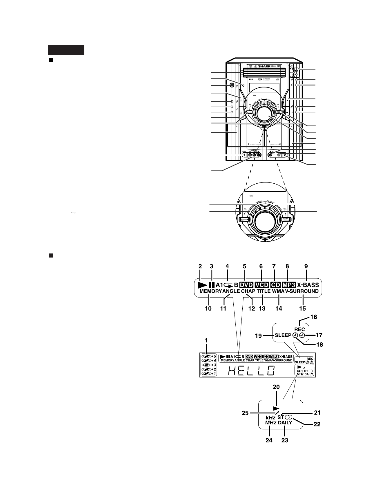
[2] Names of parts
CD-DV600W
Front panel
1. Disc Trays
2. Timer Set Indicator
3. On/Stand-by Button
4. DVD Chapter Skip/DVD/Video CD/CD/MP3/WMA Track Up or
Fast Forward, Tape 2 Fast Forward, Tuner Preset Up,
Time Up Button
5. Clock/Timer Button
6. Tuning Up Button
7. Tuning Down Button
8. DVD Chapter Skip/DVD/Video CD/CD/MP3/WMA Track Down or
Fast Reverse, Tape 2 Rewind, Tuner Preset Down, Time Down Button
9. Equalizer Mode Select Button
Tape 1 Cassette Compartment
10.
11. Headphone Socket
12.
Game/Video Input Sockets
13. Disc Number Select Buttons
14. Disc Direct Play Button
15. Disc Tray Open/Close Button
16.
DVD/Video CD/CD/MP3/WMA Play, Tape 1 Play,
Tape 2 Forward Play Button
17. Memory/Set Button
18. Tape 2 Record Pause Button
19. DVD/Video CD/CD/MP3/WMA or Tape Stop Button
20. Extra Bass/Demo Mode Button
21. Volume Control
Tape 2 Cassette Compartment
22.
23. Microphone Socket 1
24. Microphone Socket 2
25. Microphone Level
26. Tuner (Band) Button
DVD/CD Button
27.
28. Tape (1 2) Button
29. Game/Video Button
10
11
12
27
26
1
2
3
4
DVDMINI SYSTEM
CD-DV600
5
6
7
13
14
15
16
17
18
8
9
19
20
21
22
MIC
1 2
MICLEVEL
MIN MAX
23
24
25
CD-DV600
28
29
Display
1. Disc Number Indicators
2. DVD/Video CD/CD/MP3/WMA Play Indicator
3. DVD/Video CD/CD/MP3/WMA Pause Indicator
4. DVD/Video CD/CD/MP3/WMA Repeat Indicator
5. DVD Indicator
6. VCD Indicator
7. CD Indicator
8. MP3 Indicator
9. Extra Bass Indicator
10. Memory Indicator
11. DVD Angle Indicator
12. DVD Chapter Indicator
13. DVD Title Indicator
14. WMA Indicator
15. Virtual Surround Indicator
16. Tape 2 Record Indicator
17. Timer Recording Indicator
18. Timer Play Indicator
19. Sleep Indicator
20. Tape 1 Play or Tape 2 Forward Play Indicator
21. FM Stereo Mode Indicator
22. FM Stereo Receiving Indicator
23. Daily Timer Indicator
24. Tuner Receiving Frequency Indicators
25. Karaoke Mode Indicator
1 – 2
Page 5
CD-DV600W
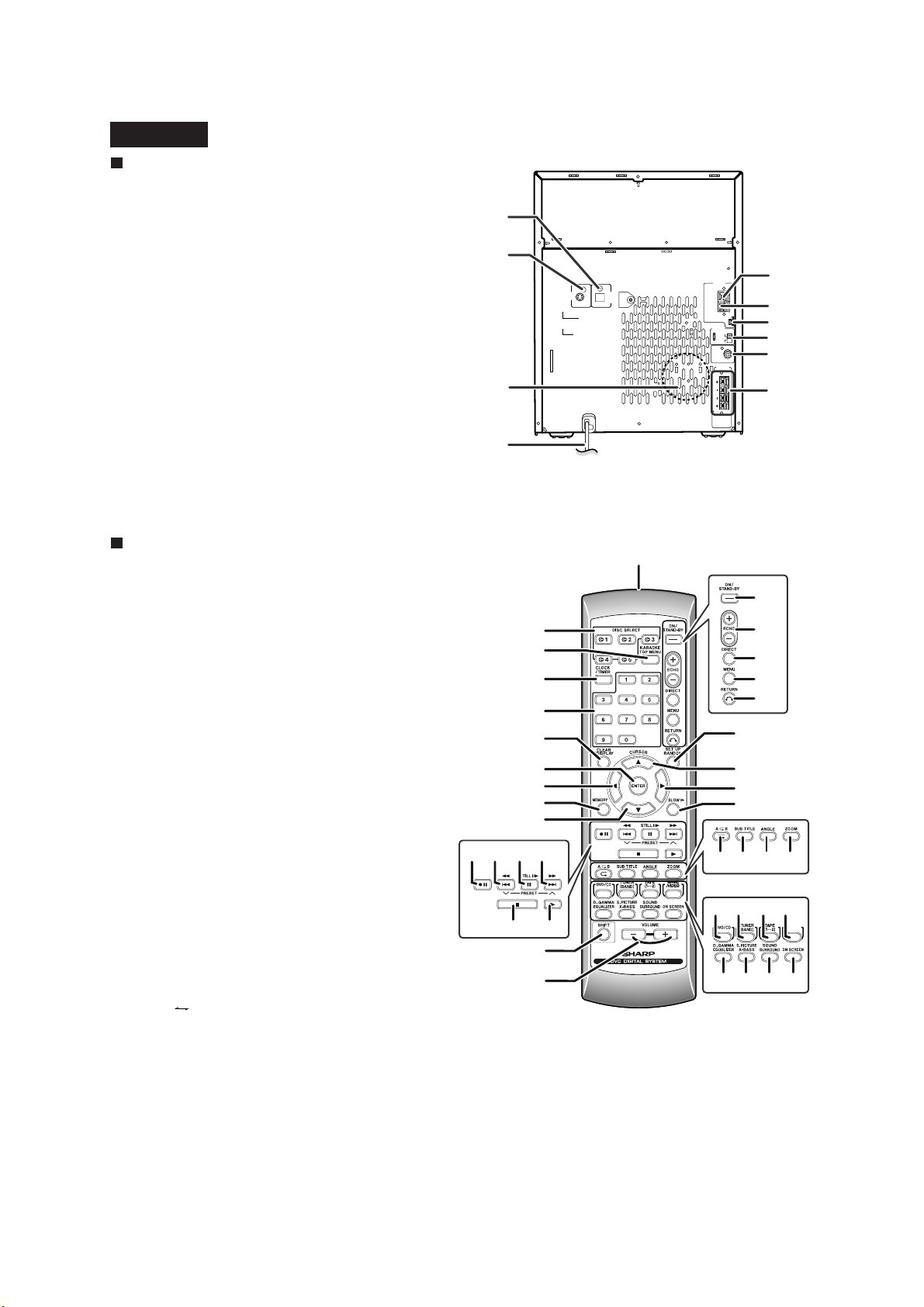
Rear panel
1. Audio Digital Out Socket
2. S-Video Output Socket
3. Cooling Fan
4. AC Power Lead
5. FM 75 Ohm Aerial Terminal
6. FM Aerial Earth Terminal
7. AM Loop Aerial Socket
8. Span Selector Switch
9. Video Output Socket
10. Speaker Terminals
CD-DV600W
1
2
AIITENNA
S-VIDEO
AUDIO
OUT
DIGITAL
OUT
DVD/CD
3
AC INPUT
FM
75CHMS
GND
AM
LOOP
SPAN
SELECTOR
FM/AM(kHz)
50/9
100/10
VIDEO
OUT
SPEAKERS
LEFT RIGHT
RATEDSPEAKER
IMPENANCE:
6OHMSMIN.
5
6
7
8
9
10
4
Remote control
1. Remote Control Transmitter
2. Disc Number Select Buttons
3. DVD Top Menu Button
4. Clock/Timer Button
5. Direct Search Buttons
6. Clear/Display Button
7. Enter Button
8. Cursor Left Button
9. Memory/Dimmer Button
10. Cursor Down Button
11. Tape 2 Record Pause Button
12.
DVD Chapter Skip, DVD/Video CD/CD/MP3/WMA Fast Reverse,
Video CD/CD/MP3/WMA Track Down, Tape 2 Fast Wind and
Tuner Preset Down, Time Down Button
13. DVD/Video CD/CD/MP3/WMA Pause Button
14.
DVD Chapter Skip, DVD/Video CD/CD/MP3/WMA Fast Forward,
Video CD/
Tuner Preset Up, Time Up Button
15. DVD/Video CD/CD/MP3/WMA/Tape Stop Button
16. DVD/Video CD/CD/MP3/WMA/Tape 1 Play,
Tape 2 Forward Play Button
17. Shift Button
18. Volume Up/Down Buttons
19. On/Stand-by Button
20. Echo Level Up/Down Buttons
21. DVD Direct Button
22. DVD Menu Button
23. Return Button
24. CD Random Button
25. Cursor Up Button
26. Cursor Right Button
27. DVD/Video CD Slow Button
28. DVD/Video CD/CD/MP3/WMA Repeat Button
29. DVD Subtitle Button
30. DVD Angle Button
31. DVD Zoom Button
32. DVD/Video CD/CD/MP3/WMA Button
33. Tuner (Band) Button
34. Tape (1
35. Game/Video Button
36. Equalizer Mode Select Button
37. Extra Bass Button
38. DVD 3-D Virtual Surround Button
39. DVD On Screen Button
CD/MP3/WMA Track Up, Tape 2 Fast Wind and
2) Button
12 13 14
11
2
3
4
5
6
7
8
9
10
15 16
17
18
1
RRMCGA033AWSA
19
20
21
22
23
24
25
26
27
28 29 30 31
32 33 34 35
36 37 38 39
GAME
/VIDEO
1 – 3
Page 6
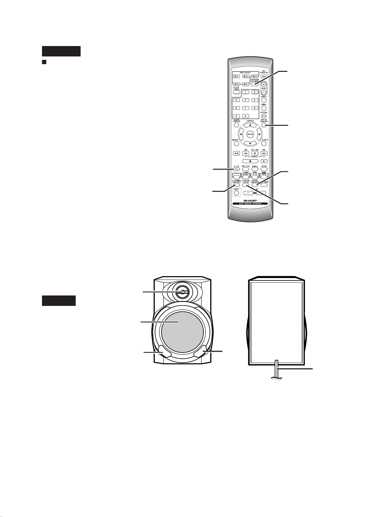
CD-DV600W
CD-DV600W
Remote control with shift button
1. Karaoke/Audio Mode Button
2. DVD Setup Button
3. DVD Sound Button
4. DVD Super Picture Button
5. DVD/Video CD/CD A-B Repeat Button
6. DVD Digital Gamma Button
1
2
CP-DV600
1. Tweeter
2. Woofer
3. Super Tweeters
4. Speaker Wire
5
3
6
RRMCGA033AWSA
4
1
2
1 – 4
33
4
Page 7
AM IF
FM RF
TP301
TP302
FM IF
T301
T302
R356
R381
T303
T306
IC301
L312
T351
CNP301
AM/FM LOOP ANTENNA
FM BAND
COVERAGE fL
AM BAND
COVERAGE fL
AM TRACKING
fL
MAIN PWB
1
AudioCD-DV999W/CD-DV777WService ManualCD-DV999W/CD-DV777WMarketE
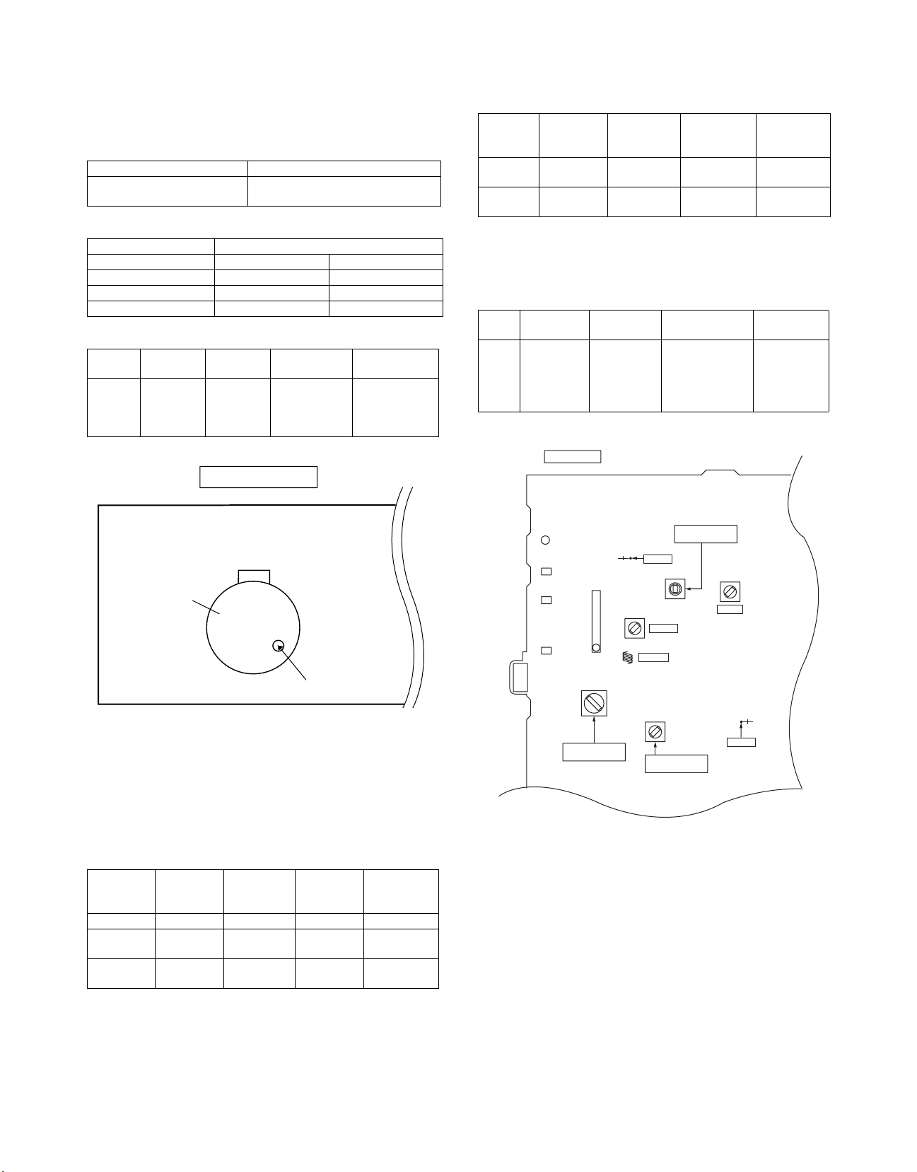
CHAPTER 2. ADJUSTMENTS
CD-DV600W
•FM RF
Signal generator: 1 kHz, 40 kHz dev., FM modulated
[1] Mechanism section
• Driving Force Check
Torque Meter Specified Value
Play: TW-2111 Tape 1: Over 80 g
Tape 2: Over 80 g
• Torque Check
Torque Meter Specified Value
Tape 1 Tape 2
Play: TW-2111 30 to 80 g.cm 30 to 80 g.cm
Fast forward: TW-2231 — 70 to 180 g.cm
— 70 to 180 g.cm
• Tape Speed
Normal
speed
Test Tape Adjust-
ing Point
MT T-111 Var iable
Resistor in
motor.
TAPE MECHANISM
Specified
Val ue
3,000 ± 30 Hz
Speaker
Instrument
Connection
Speaker Terminal (Load
resistance: 6
ohms)
Test
Stage
Frequency Frequency
Display
Setting/
Adjusting
Point
FM Band
Coverage
FM RF 98.00 MHz
— 87.50 MHz T301 (fL):
1.2 V ± 0.1 V
98.00 MHz L312 *2
(10-30 dB)
*1. Input: Antenna Output: TP301
*2. Input: Antenna Output: Speaker terminal
•FM IF
Signal generator: 10.7 MHz, FM modulated
Test
Stage
Frequency Frequency
Display
Setting/Adjust-
ing Point
IF 10.7 MHz 98 MHz T302 (Turn the
core of transformer T302
fully counter
clockwise)
Instrument
Connection
*1
Instrument
Connection
*1
Tape
Motor
Variable Resistor in motor
Figure 1
[2] Tuner section
fL: Low-range frequency
fH: High-range frequency
• AM IF/RF
Signal generator: 400 Hz, 30%, AM modulated
Test Stage Frequency Frequency
AM IF 450 kHz 1,602 kHz T351 *1
AM Band
Coverage
AM
Tracking
*1. Input: Antenna Output: TP302
*2. Input: Antenna Output: TP301
Display
— 531 kHz (fL): T306
990 kHz 990 kHz (fL): T303 *1
Setting/
Adjusting
1.1 ± 0.1 V
Figure 2 Adjustment Points
Instrument
Connection
Parts
*2
2 – 1
Page 8

CD-DV600W
[3] DVD/CD section
1. DVD SECTION
• Adjustment
Since this DVD system incorporates the following automatic adjustment functions, readjustment is not needed when replacing the
pickup. Therefore, different PWBs and pickups can be combined
freely.
Each time a disc is changed, these adjustments are performed
automatically. Therefore, playback of each disc can be performed
under optimum conditions.
Items adjusted automatically
1) Offset adjustment (The offset voltage between the head amplifier
output and the VREF reference voltage is compensated inside the
IC.)
* Focus offset adjustment
* Tracking offset adjustment
2) Tracking balance adjustment
3) Gain adjustment (The gain is compensated inside the IC so that the
loop gain at the gain crossover frequency will be 0 dB.)
* Focus gain adjustment
* Tracking gain adjustment
DVD/CD Error code description
Error Explanation
10* CAM error. Can't detect CAM switch when CAM is moving.
11* When it detect cam operation error during initialize pro-
cess.
20* TRAY error. Can't detect TRAY switch when TRAY is mov-
ing.
21* When it detect TRAY operation error during initialize pro-
cess.
30 When it change to DVD/CD function, DVD cannot read ini-
tial data.
* 'CHECKING'
If Error is detected, 'CHECKING' will be displayed instead of 'ERCD**'. 'ER-CD**' display will only be displayed when error had been
detected for the 5th times.
2 – 2
Page 9
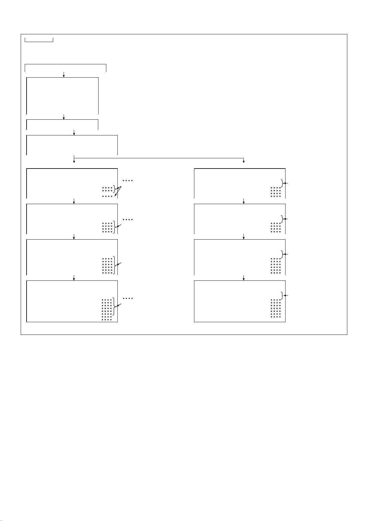
[4] TEST Mode
1. DVD TEST Mode
1. Press the DVD/CD button on the main unit from the TEST mode
initial condition to enter "DVD TEST".
CD-DV600W
F0000000 00000000
(Press the "1" key of the remote control.)
TEST MODE
Model name (MODEL)
Program version/
Creation date
CPRM key code
(CPRM)
CPRM Serial No.
(S/N)
Microcode
version (UCODE)
Servo program version
(SODCV)
Source code
version (CSTMV)
FFFF FFFF
FFFF FFFFFF
RO*: Region No.
Press the "PLAY" key of the remote control 8 times.
TEST Mode initial screen returns.
(TEST Mode initial screen)
LASER TEST Mode
Press the DVD/CD button on the main unit from the TEST mode
1.
initial condition to enter "DVD TEST".
F0000000 00000000
Press the (3) key.
DYNAMIC TEST
1 : LASER TEST
2:STEP TEST
3:PLAY TEST
3 : PLAY TEST NO TRAY
M E N U : SPIN OFFSET ADJUST
Press the (1) key. Press the (1) key.
LASER TEST
DVD LD ON
(TEST MODE initial screen)
The screen display as shown on the left.
The tray opens and DVD
laser lights on.
The spin rotates
approx. 1 sec.
The pick slightly moves
in the circumference
direction.
Press the (1) key.
LASER TEST
CD LD ON
LASER TEST
LD OFF
DVD laser lights off and
CD laser lights on.
The spin rotates approx.
1 sec.
The pick slightly moves in
the circumference direction.
Laser lights off.
The spin rotates approx.
1sec.
The pick slightly moves in
the circumference direction.
Press the (1) key to shift to "DVD LD ON".
Press the "STOP" key to return to the "DYNAMIC TEST" screen.
2 – 3
Page 10
CD-DV600W
Step Execute Mode
1. Press the DVD/CD button on the main unit from the TEST mode
initial condition to enter "DVD TEST".
F0000000 00000000
Press the (3) key.
DYNAMIC TEST
1:LASER TEST
2:STEP TEST
3:PLAY TEST
9:PLAY TEST NO TRAY
MENU : SPIN OFFSET ADJUST
Press the (2) key.
STEP TEST
TRAY OPEN
Press the "PLAY" key.
STEP TEST
FOCUS ON
4-digit alphanumeric
ASMAX
4-digit alphanumeric
FEPP
Press the "PLAY" key.
STEP TEST
TRACK ING ON
ASMAX
4-digit alphanumeric
FEPP
4-digit alphanumeric
ASAGC
4-digit alphanumeric
TEAGC
4-digit alphanumeric
FBAL0
0000
TBAL0
Press the "PLAY" key.
Press the "PLAY" key.
Press the "PLAY" key.
Press the "STOP" key to return to the DYNAMIC TEST screen.
Turn the power from off to on to clear the Step Execute Mode.
4-digit alphanumeric
STEP TEST
FBAL STUDY
ASMAX
4-digit alphanumeric
FEPP
4-digit alphanumeric
ASAGC
4-digit alphanumeric
TEAGC
4-digit alphanumeric
FBAL0
4-digit alphanumeric
TBAL0
4-digit alphanumeric
STEP TEST
GAIN STUDY
4-digit alphanumeric
ASMAX
4-digit alphanumeric
FEPP
4-digit alphanumeric
ASAGC
4-digit alphanumeric
TEAGC
4-digit alphanumeric
FBAL0
4-digit alphanumeric
TBAL0
4-digit alphanumeric
FCGA0
4-digit alphanumeric
TKGA0
STEP TEST
D V D I D 8-digit numeric
4-digit alphanumeric
ASMAX
4-digit alphanumeric
FEPP
4-digit alphanumeric
ASAGC
4-digit alphanumeric
TEAGC
4-digit alphanumeric
FBAL0
4-digit alphanumeric
TBAL0
4-digit alphanumeric
FCGA0
4-digit alphanumeric
TKGA0
4-digit alphanumeric
FCBT0
4-digit alphanumeric
OFTR0
4-digit alphanumeric
4-digit alphanumeric
DVD CD
4-digit alphanumeric
4-digit alphanumeric
ASAGC
TEAGC
FBAL1
TBAL1
4-digit alphanumeric
4-digit alphanumeric
ASAGC
TEAGC
FBAL1
TBAL1
4-digit alphanumeric
4-digit alphanumeric
ASAGC
TEAGC
FBAL1
TBAL1
FCGA1
TKGA1
4-digit alphanumeric
4-digit alphanumeric
ASAGC
TEAGC
FBAL1
TBAL1
FCGA1
TKGA1
FCBT1
OFTR1
(TEST MODE initial screen).
The screen display as shown on the left.
The tray opens. Put the disc on the tray.
Focus On.
0000
0000
Tracking On.
0000
0000
0000
0000
0000
0000
0000
0000
0000
" ": 4-digit alphanumeric also
displayed for DVD double deck disc.
Focus balance adjustment values displayed.
" ": 4-digit alphanumeric also displayed for
DVDdoubledeckdisc.
Focus tracking gain adjustment values displayed.
4-digit alphanumeric also displayed for "****"
in the case of DVD double deck disc.
Equalizer adjustment values and Off-track Level
adjustment values displayed. 8-digit numeric of
DVDIDgrows.
" ": 4-digit alphanumeric also displayed
for DVD double deck disc.
Press the "PLAY" key.
STEP TEST
TRACK ING ON
ASMAX
4-digit alphanumeric
FEPP
4-digit alphanumeric
ASAGC
4-digit alphanumeric
TEAGC
4-digit alphanumeric
FBAL0
0000
TBAL0
Press the "PLAY" key.
Press the "PLAY" key.
Press the "PLAY" key.
Press the "STOP" key to return to the DYNAMIC TEST screen.
Turn power from off to on to clear the Step Execute Mode.
4-digit alphanumeric
STEP TEST
FBAL STUDY
ASMAX
4-digit alphanumeric
FEPP
4-digit alphanumeric
ASAGC
4-digit alphanumeric
TEAGC
4-digit alphanumeric
FBAL0
4-digit alphanumeric
TBAL0
4-digit alphanumeric
STEP TEST
GAIN STUDY
4-digit alphanumeric
ASMAX
4-digit alphanumeric
FEPP
4-digit alphanumeric
ASAGC
4-digit alphanumeric
TEAGC
4-digit alphanumeric
FBAL0
4-digit alphanumeric
TBAL0
4-digit alphanumeric
FCGA0
4-digit alphanumeric
TKGA0
STEP TEST
C D N O 2-digit numeric T I M E 6-digit numeric
4-digit alphanumeric
ASMAX
4-digit alphanumeric
FEPP
4-digit alphanumeric
ASAGC
4-digit alphanumeric
TEAGC
4-digit alphanumeric
FBAL0
4-digit alphanumeric
TBAL0
4-digit alphanumeric
FCGA0
4-digit alphanumeric
TKGA0
4-digit alphanumeric
FCBT0
4-digit alphanumeric
TEOFS
4-digit alphanumeric
4-digit alphanumeric
ASAGC
TEAGC
FBAL1
TBAL1
4-digit alphanumeric
4-digit alphanumeric
ASAGC
TEAGC
FBAL1
TBAL1
4-digit alphanumeric
4-digit alphanumeric
ASAGC
TEAGC
FBAL1
TBAL1
FCGA1
TKGA1
4-digit alphanumeric
4-digit alphanumeric
ASAGC
TEAGC
FBAL1
TBAL1
FCGA1
TKGA1
FCBT1
TEOFS
4-digit alphanumeric
Tracking On.
0000
"0000": 4-digit alphanumeric
0000
also displayed for CD-RW.
Focus balance adjustment
values displayed.
0000
"0000": 4-digit alphanumeric
0000
also displayed for CD-RW.
Focus tracking gain adjustment
values displayed.
0000
"0000": 4-digit alphanumeric
0000
also displayed for CD-RW.
Equalizer adjustment value and
TES signal offset displayed.
6-digit numeric of the TIME counter grows.
0000
"0000": 4-digit alphanumeric
0000
also displayed for CD-RW.
2 – 4
Page 11
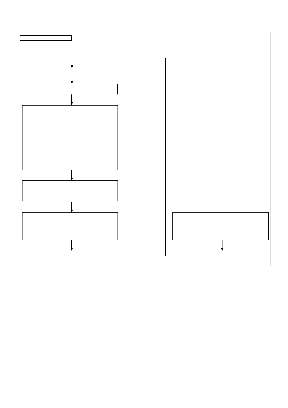
Spin Offset Adjustment Mode
Note 1: After replacing the DVD main PWB unit and the DVD mechanism chassis unit,
be sure to adjust spin offset.
Start from "NO DISC" (the tray closed).
CD-DV600W
F0000000 00000000
Press the "3" key.
DYNAMIC TEST
1:LASER TEST
2:STEP TEST
3:PLAY TEST
3:PLAY TEST NO TRAY
M E N U:SPIN OFFSET ADJUST
Press the "MENU" key.
SPIN OFFSET ADJUST
SPIN AD OFFSET
SPIN OFFSET TEST
ADJUST COMPLETE
SPIN 4-digit alphanumeric
The screen display as
shown on the left
The screen display as
shown on the left
Tray opens.
Adjustment started
4-digit alphanumeric
displayed
Failure
SPIN OFFSET TEST
ADJUST FAILED
2 – 5
Turn off the power and clear the Spin Offset Adjustment
Mode to try again from the start.
Page 12
CD-DV600W
2. List of Keys Used for DVD TEST Mode and Transmit Key Codes to the Unit
Button for System
Communication
C-PLAY Play 26h
C-PAUSE/STILL
(Remote Control)
C-STOP (Remote control) Stop 27h
C-STOP (Main Unit) Stop 27h
SKIP-UP/CUE Skip+ 2Ch In this TEST Mode Skip+/Next button code (2Ch) is constantly transferred.
SKIP-DWN/REV Skip- 2Bh In this TEST Mode Skip-/Prev button code (2Bh) is constantly transferred.
SKIP-UP
(Remote Control)
SKIP-DWN
(Remote Control)
REPEAT (Remote Control) Repeat 32h
A-B repeat
(Remote Control)
PROGRAM
(Remote Control)
“1” key (Remote Control) 1 01h
“2” key (Remote Control) 2 02h
“3” key (Remote Control) 3 03h
“4” key (Remote Control) 4 04h
“5” key (Remote Control) 5 05h
“6” key (Remote Control) 6 06h
“7” key (Remote Control) 7 07h
“8” key (Remote Control) 8 08h
“9” key (Remote Control) 9 09h
“0” key (Remote Control) 0 0Ah
ENTER (Remote Control) Enter 70h
MENU (Remote Control) MENU 68h
SLOW> (Remote Control) SLOW> 72h
Buttons used for the TEST Mode are shown above. When pressing the following DVD-related buttons, corresponding button codes are transmitted.
ON SCREEN, SURROUND, CUE, REVIEW, Curser ↑, ↓, ←, →, RETURN, ZOOM, TOP-MENU, CLEAR, RANDOM subtitle, angle, sound, DVD
MENU, Gamma, S-picture, DIRECT, DISPLAY, SET-UP.
Button Code Button Code
HEX Value
Pause/still 29h
Skip+ 2Ch
Skip- 2Bh
A-B Repeat 49h
Program 1Fh
Remarks
Supplementary Note
1. Do not press buttons other than the DVD-related buttons, except for the Power button. Do not switch functions; do not control volumes.
For the electronic volume IC and the monitor output control, constantly fix the setting to DVD/CD function.
2 – 6
Page 13
3. ROM Rewrite Mode
Description of version name
Example: VER: VXW0223A
From the left:
V : Video model
X : CD-DV***W
W : Southeast Asia
0223A:Version
* The format may be changed.
ex)VXW0223A
2 Destination
1 Model
V: Video model/A: Audio/Model for SACD
X : CD-DV***W
1 Model
J : Japan
H : Europe
U: USA
K : Korea/Philippines
W : Southeast Asia
A : Australia
Z : Middle East
C : China
M : Mexico
2 Destination
1. Creating version upgrade disc
• Write the following three files on CD-R/CD-RW.
• !$#%&’().@{}
• D-combo3.cdr
• ********.bin
(********: Names differ according to versions)
• Write the files at lowest possible speed.
• Do not mix other data.
2. During normal power-on, insert the version upgrade disc.
3. After the version upgrade disc is normally determined, the message, “VERSION UP DISC IS DETECTED” and the version are displayed on OSD. Then ROM data read is started.
OSD display (Example)
VERSION UP DISC
IS DETECTED
0905
CD-DV600W
7. Confirming the version
• A few moments after entering the DVD TEST Mode, “DVD ****”
is displayed on the main unit.
(****: 4-digit numeric version code)
• To confirm the detailed version information, press the “1” key of
the remote control.
The system information is displayed on the OSD display.
(“********”: Version name) Check that the version name conforms to the write data.
4. When the data read is completed, “NOW FLASH WRITE START…”
is displayed on OSD. Then the Flash Rom rewrite is entered.
OSD display (Example)
5. When rewrite is normally completed, “FL W: END” is displayed on
the main unit. Eject the disc automatically coming out from the tray.
Then turn the power off.
6. If “FL W: ERR” or “CANT READ” is displayed on the main unit or
“FL W: END” is not displayed after 10 minutes, turn the power off to
try again from the start.
NOW FLASH WRITE START...
ROM DATA READING
956
VERSION UP DISC
IS DETECTED
0905
8. Press the POWER button to display “CLEAR AL”
• Reset and start the system’s microcomputer to cancel the TEST
Mode.
READ COMPLETE
2 – 7
Page 14

CD-DV600W
4. DVD Display Test
To display servo adjustment values, error rates, laser current, etc. during DVD playback.
1. Press the DISC 2 button on the main unit from the TEST Mode initial condition.
2. DVD starts up with “DVD” blinking on the FL display.
3. Press the Tuner/Band button to display DVD adjustment values, etc. Press it again and the display disappears and the normal screen returns.
The error rates displayed are for reference; they are not the judging criteria.
4. Press the “Power” button to cancel this mode.
DVD
FG0 TG0 TG1FG1 FBL0 TBL0 TBL1FBL1
Average error rate
Audio buffer space Video buffer space Number of error occurrence
TitleNo ChapNo
CD
Audio buffer space Video buffer space Number of error occurrence
TrNo TIME
When the Spin Offset Mode is never executed
DVD
FG0
Average error rate
Maximum error rate Laser output
Sector ID
Maximum error rat Laser output
TG0 TG1FG1 FBL0 TBL0 TBL1FBL1
SPIN READ NG
Audio buffer space Video buffer space Number of error occurrence
TitleNo ChapNo Sector ID
CD
Audio buffer space Video buffer space Number of error occurrence
TrNo TIME
2 – 8
Page 15
5. CD-ROM Write Mode
F
z
1. Outline
DVD-ROM can be upgraded from CD-ROM. The write mode is
entered from the normal mode.
1. When any CD-ROM for version upgrade DVD is detected, the status informs that the version upgrade ROM is being read.
When DVD microcomputer is changed to System microcomputer
and byte 24 status data detects 0Fh:
• The TEST Mode is entered by the status reception. (Required to
be internally recognized.)
• The Power button /Function switching is prohibited.
(Power supply is necessary until write is completed.)
• It is prohibited to accept any button input until write is com-
pleted.
• Change the display as follows:
TOC READ
Standard Specification of Stereo System Error Message Display Contents
Error Contents Display Notes
CD CD Changer Mechanism Error. 'ER-CD**' (*) 10: CAM SW Detection NG during normal operation
DVD Communication Error. 'ER-CD30' DVD COMMUNICATION ERROR.
Focus Not Match/IL Time Over. 'NO DISC'
TUNER PLL Unlock. PLL Unlock.
M 87.50 MH
11: CAM SW Detection NG during initialize process
20:TRAY SW Detection NG during normal operation
21:TRAY SW Detection NG during initialize process
2. To expand into RAM, DVD performs read-operation.
3. When reading ends, transmission stops for writing.
(Ignore stoppage of transmission during write.)
When transmission stops, the transmission port receives write
states, which are displayed according to port states.
DVD DATA DVD CLK State Unit display
1 L H During read FLASH W R
2 H L During write FL W : S T R
3 H H Write ended FL W : E N D
4 L L Write error FL W : E R R
4. The DVD/CD tray will automatically open when end of rewrite is
detected.
(The DVD status is not relevant since there is no communication.)
5. To close the DVD/CD door, cancel the TEST Mode and reset when
the Power button is pressed.
6. To initialize the E2PROM, do the shipping TEST Mode.
CD-DV600W
(*) CHECKING:
If CD changer mechanism error is detected, 'CHECKING' will be display instead of 'ER-CD**'. 'ER-CD**' display will only be display when
error had been detected for the 5
Speaker abnormal detection and +B PROTECTION display
In case speaker abnormal detection or +B PROTECTION had
occurred, it can be check by pressing 'POWER', ‘
button. MicroComputer version number will displayed as "UD******".
Press ‘GAME/VIDEO’ button during version number display and then
press ‘POWER’, ‘MEMORY/SET’ and ‘GAME/VIDEO’ button. Display
will show "S** B**". S is referring to speaker abnormal detection and B
is referring to +B PROTECTION. ** is in hex valve.
+B PROTECTION is condition when irregular process occur on power
supply line.
BEFORE TRANSPORTING THE UNIT
The following process need to be taken after set tapering/parts
replacement.
7. Press the ON/STAND-BY button to enter stand-by mode.
8. While pressing down the ‘
button, press the ON/STAND-BY button. The Micro Computer
version number will be displayed as "UD******".
9. Press OPEN/CLOSE button until "WAIT"→ "FINISHED" appears.
10.Unplug the AC cord and the unit is ready for transporting.
th
times.
n ' and 'X-BASS'
n' button and the X-BASS/DEMO
2 – 9
Page 16
CD-DV600W
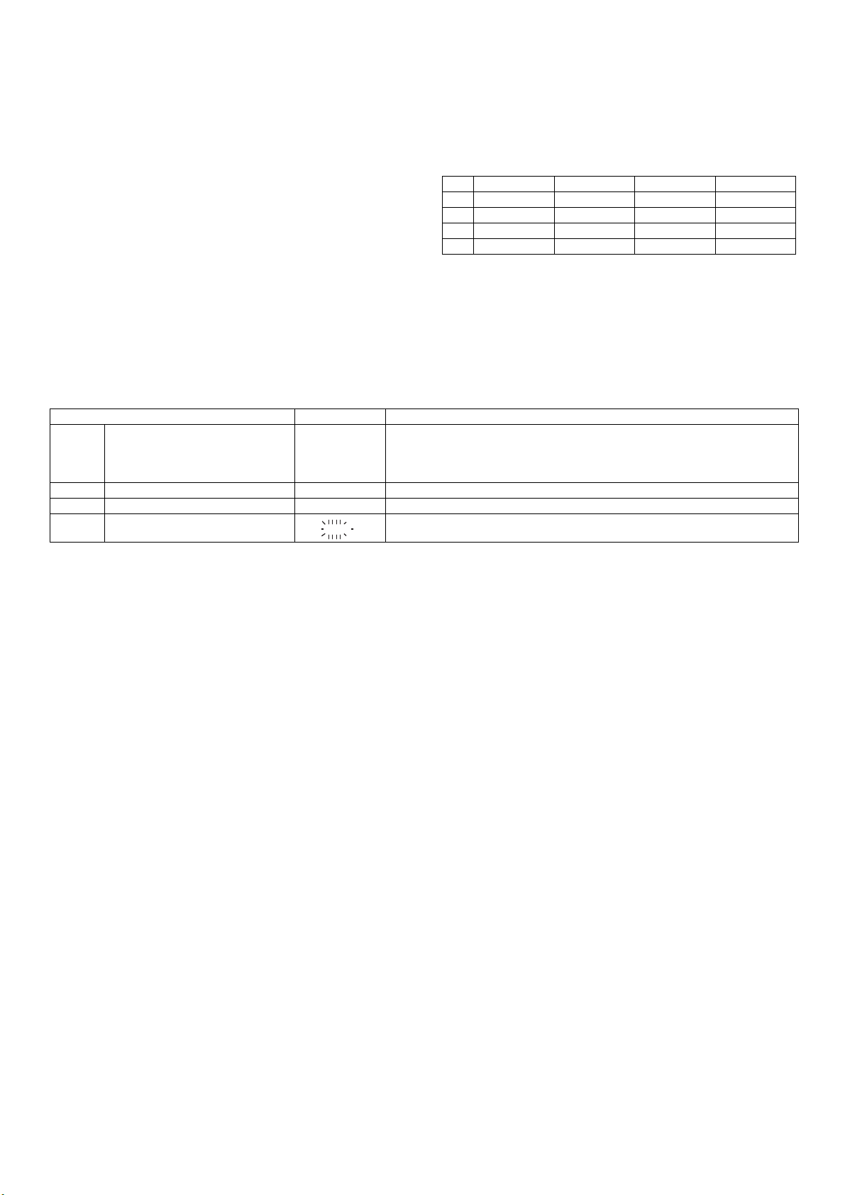
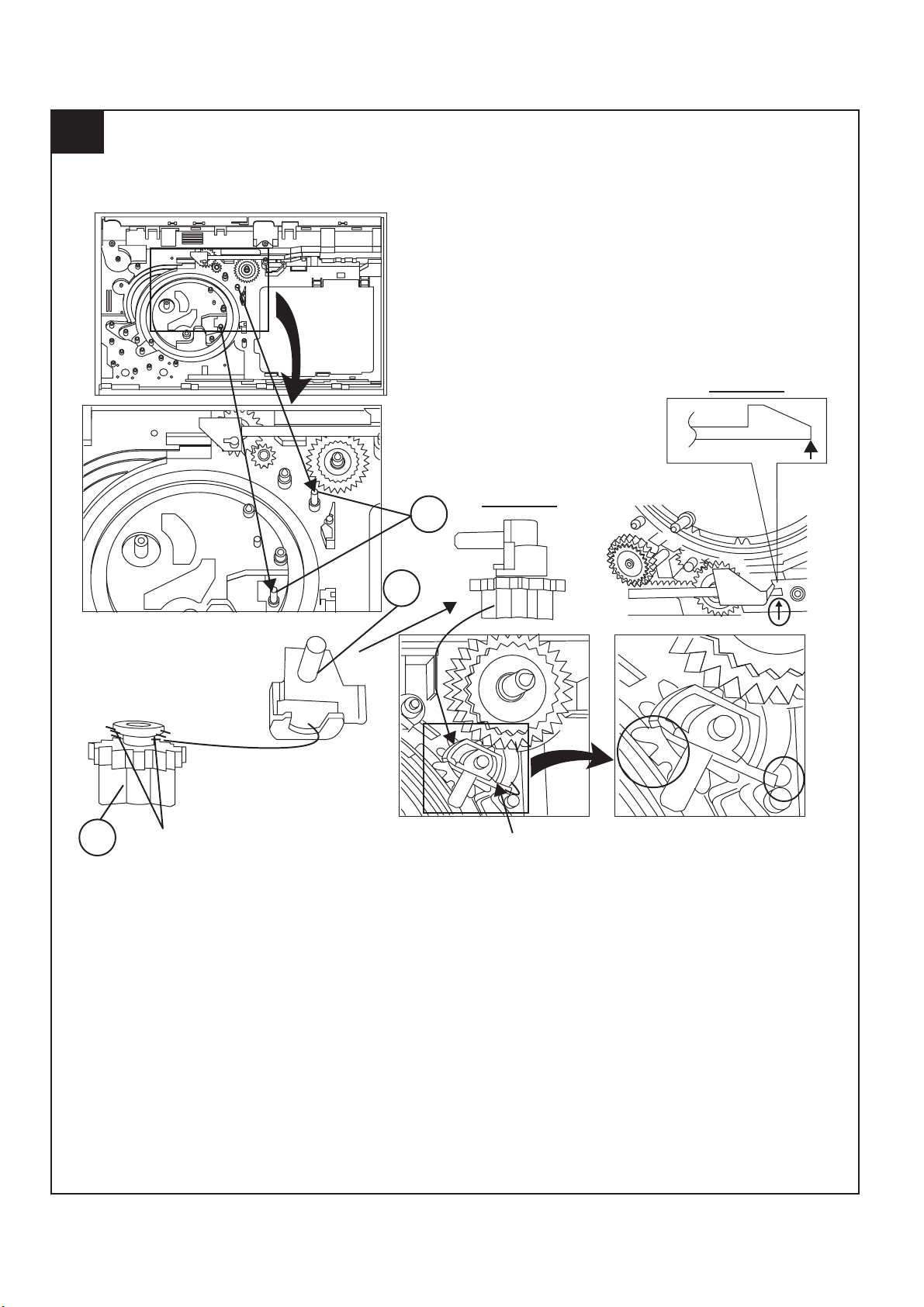
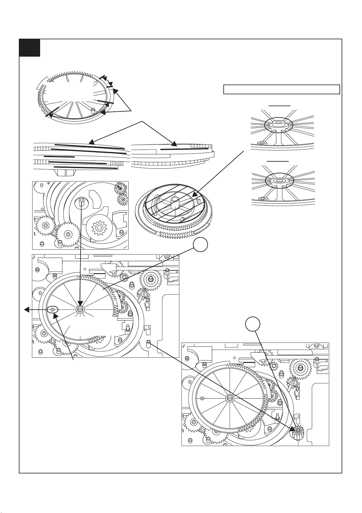
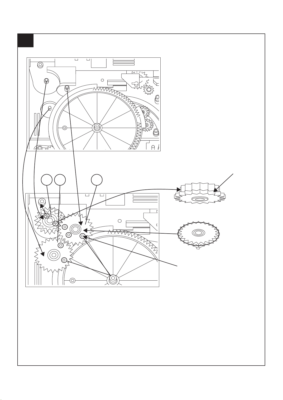
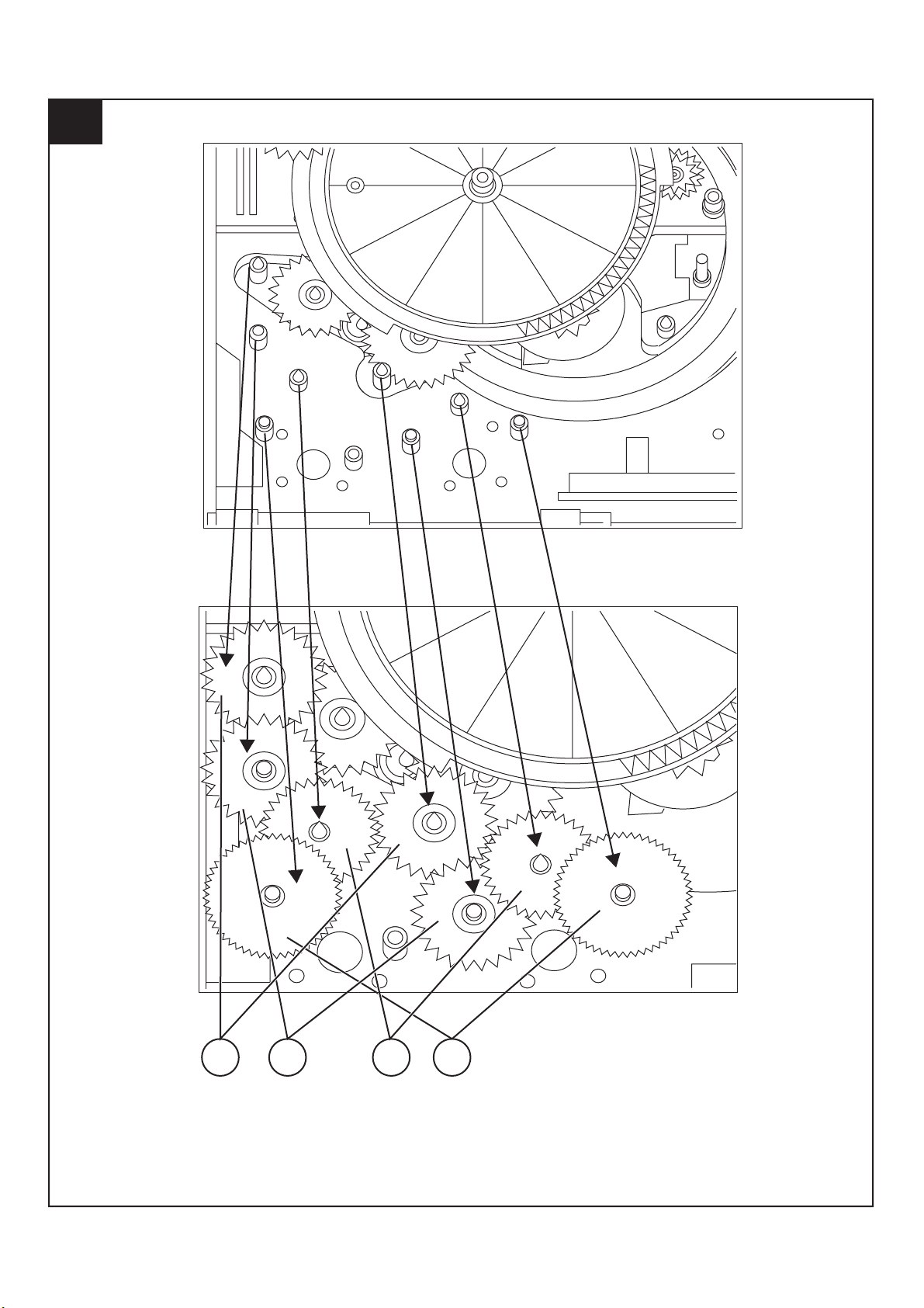
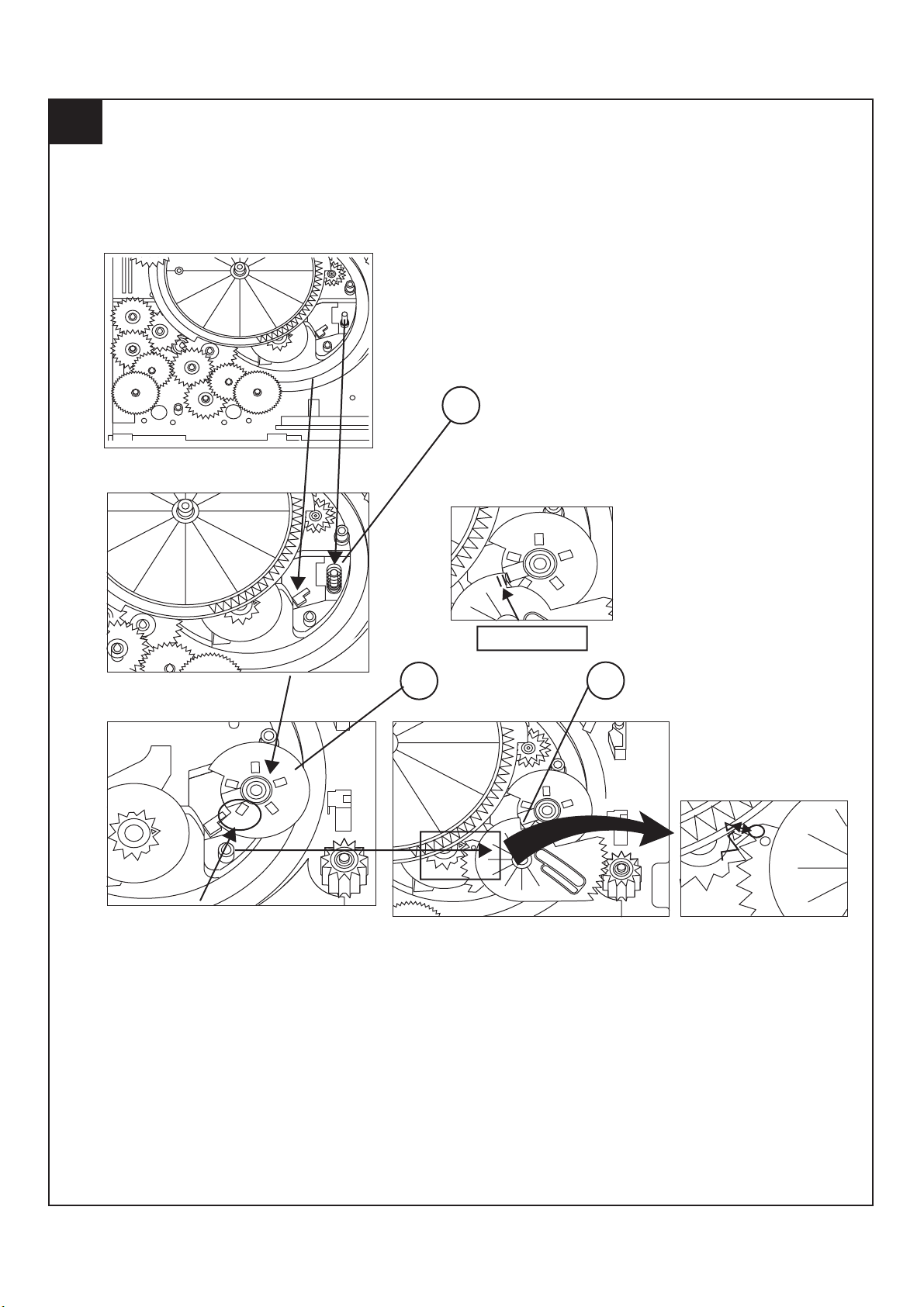
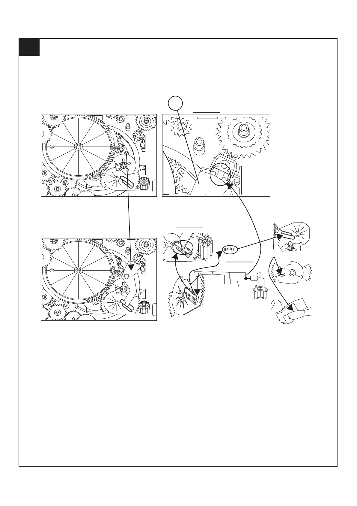
[5] CD Changer mechanism section
• A number in the drawing sheet is the number of the parts guide
(CHANGER MECHANISM PARTS).
1
141
2 – 10
140
HALF GEAR
MUST ARRANGE AS SHOWN
Page 17
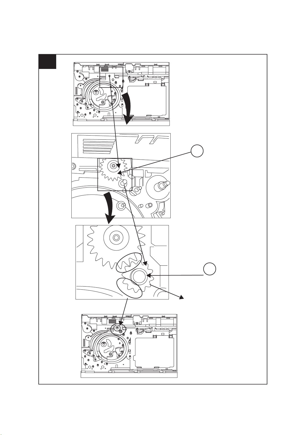
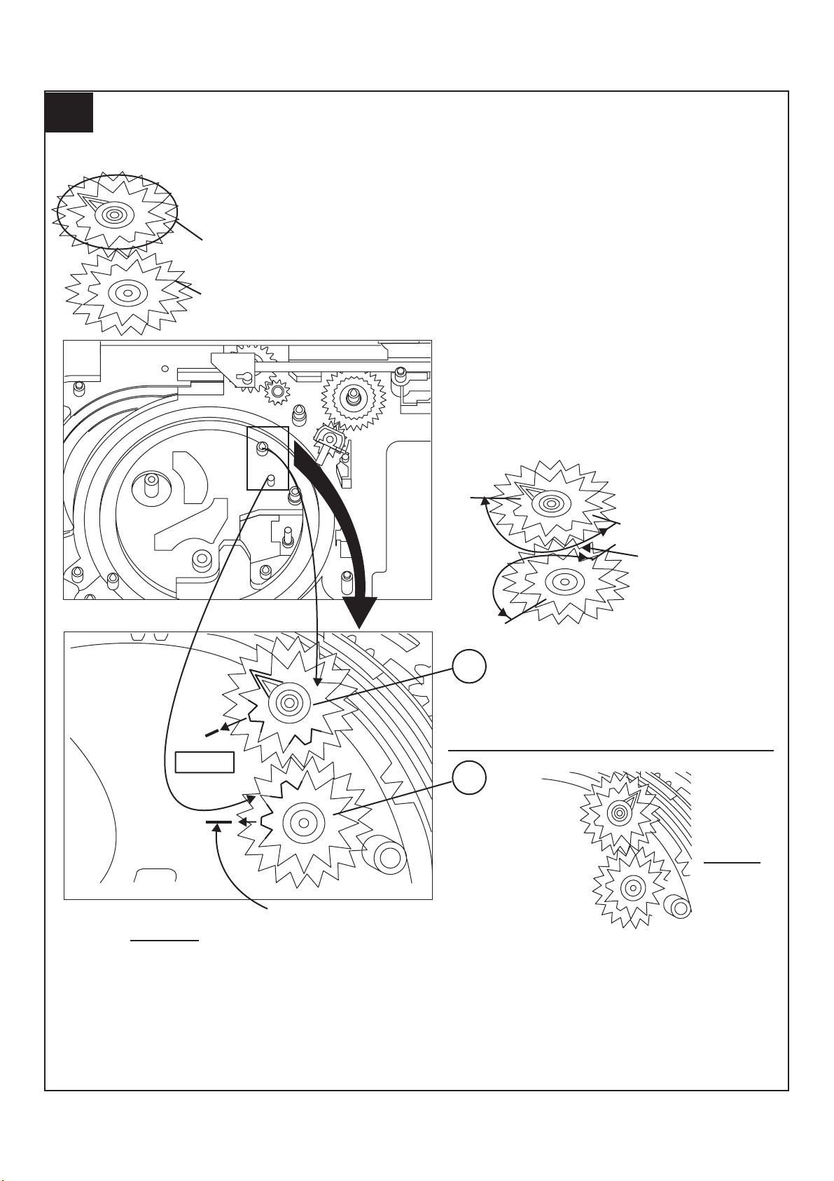
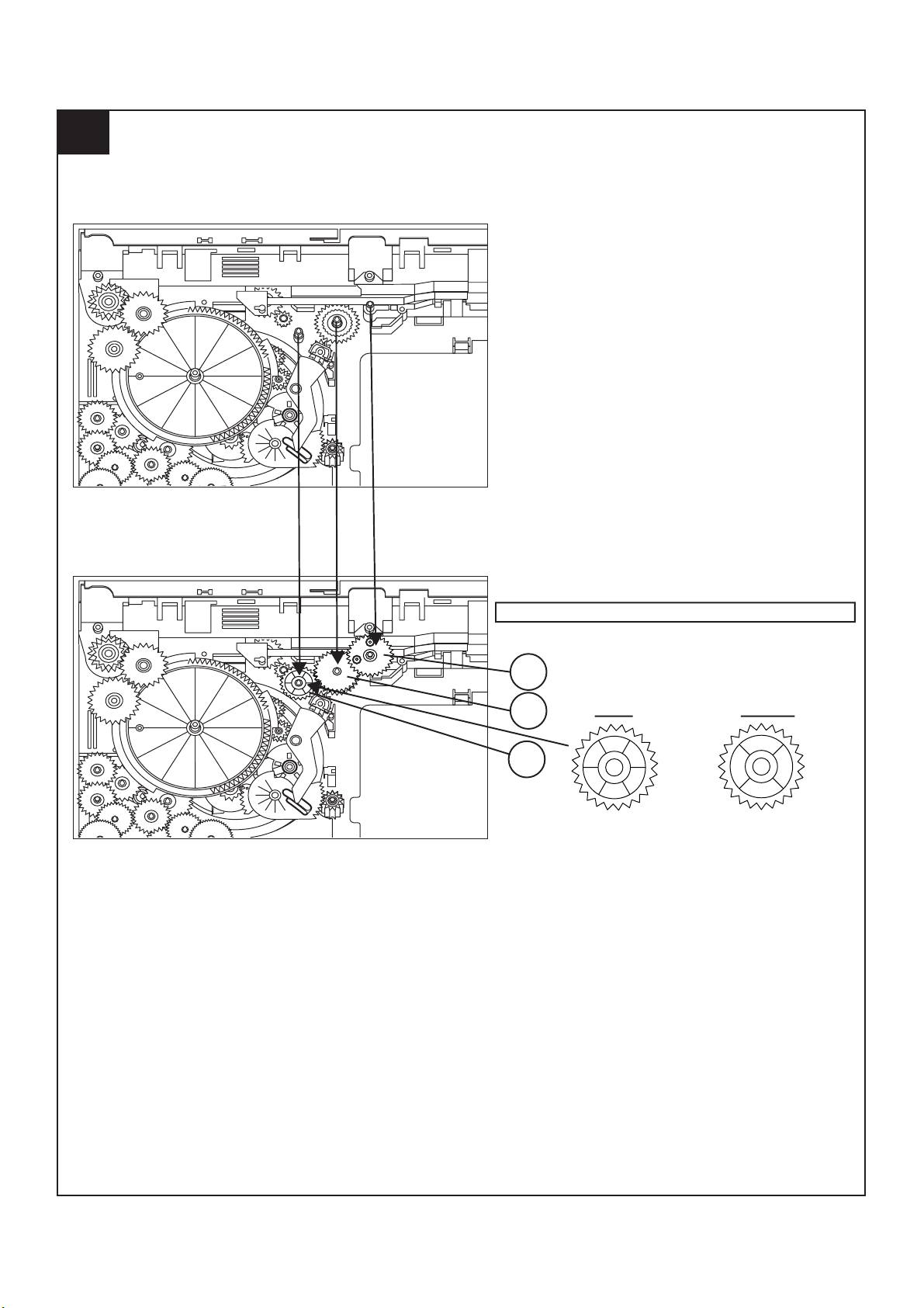
2
CD-DV600W
139
APPLY GREASE BEFORE FIX
FIX ITEM 1 ACCORDING TO THE
SHOWN PICTURE ABOVE
ROTATE MODE BIG GEAR UNTIL REACH AS SHOWN IN PICTURE
2 – 11
Page 18
CD-DV600W
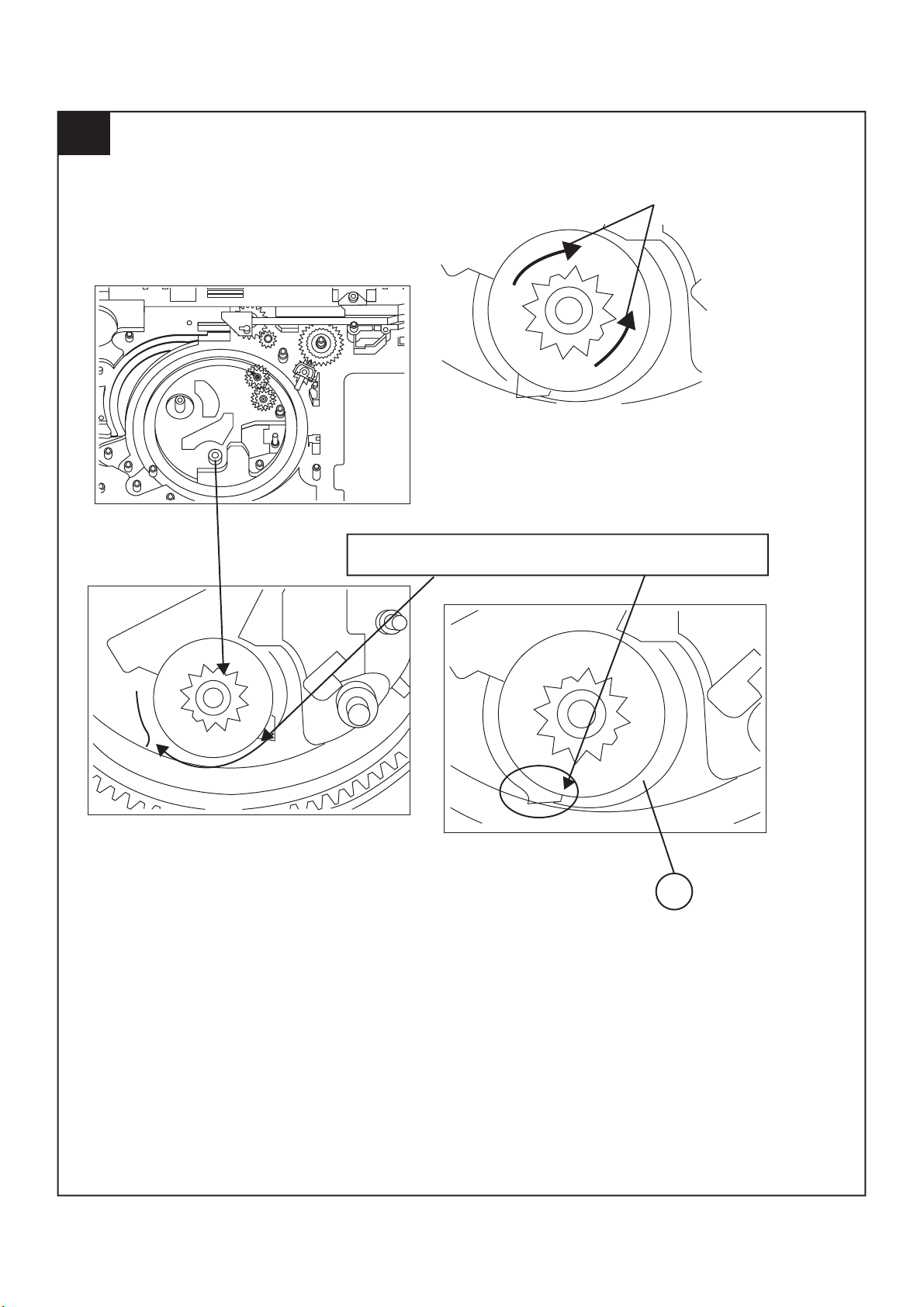
3
143
APPLY GREASE
112
PULL THE LEVER UNITIL
REACH THE ARROW MARK
2 – 12
Page 19
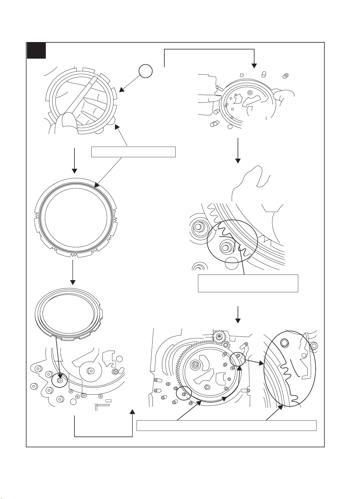
4
CD-DV600W
FIGURE 2
FIGURE 1
152
142
APPLY GREASE
118
SLOT CLAMP SW ARM INSIDE BASE SLOT
2 – 13
Page 20
CD-DV600W
5
APPLY GREASE AT BOTTOM SIDE
OF GEAR FOLLOW MARKING
NO NEED TO APPLY GREASE AT BOTTOM
SIDE
FIGURE 1
APPLY GREASE AT
TOP SIDE OF GEAR
FOLLOW MARKING
127
OTHER THAN FIGURE 1 DIRECTION ALL REJECT
O.K
128
REJECT
BLACK MARK
2 – 14
Page 21
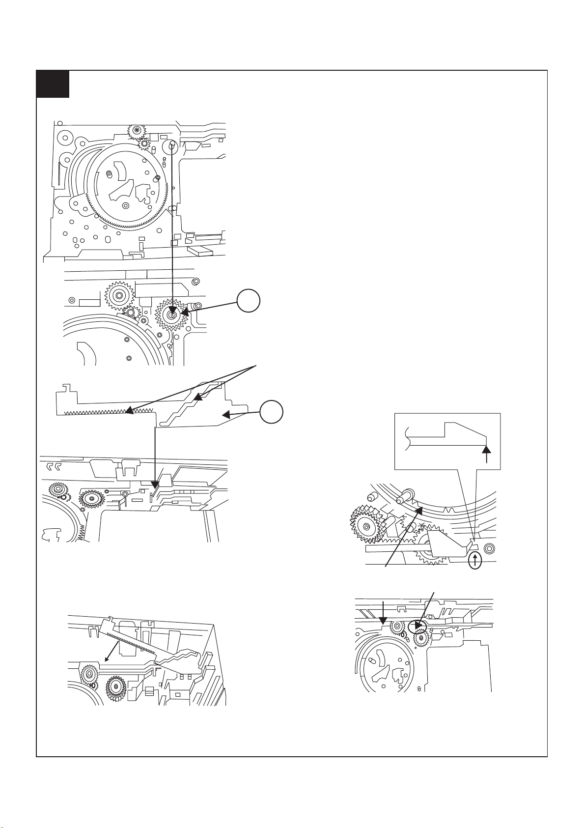
6
CD-DV600W
APPLY GREASE AT
HALF GEAR AREA
ROTATE CLOCKWISE UNTIL REACH HERE (MAXIMUM)
129
2 – 15
Page 22
CD-DV600W
7
CHANGE COLOR TO BLACK
150151148
2 – 16
Page 23
8
CD-DV600W
TRAY BIG GEAR
CHANGE COLOR
TO BLACK
MUST FREE FROM GREASE THE SHOWN AREA
O.K
GREASE APPLICATION LENGTH
GREASE APPLICATION PORTION
REJECT
124
TRAY BIG GEAR
CHANGE COLOR
TO BLACK
SHOWN HOLE MUST FACING ARROW DIRECTION
131
2 – 17
Page 24
CD-DV600W
9
138 126 125
APPLY GREASE AT
BOTTOM SIDE ONLY
TR-RE JOINT GEAR C
APPLY GREASE ONLY AT TOP SIDE GEAR
MUST FIX ACCORDING TO THE HOLE'S
2 – 18
Page 25
10
CD-DV600W
148 147 146 145
2 – 19
Page 26
CD-DV600W
11
121
WH EN FIXING ITEM 2 MUST FOLLOW AS SHOWN
144
APPLY GREASE
130
2 – 20
Page 27
12
CD-DV600W
117
FIGURE 2
FIGURE 1
APPLY GREASE
FIGURE 3
APPLY GREASE SC141
2 – 21
Page 28
CD-DV600W
13
ITEM 2 , 3 MUST APPLY GREASE ON TOP SIDE GEAR ONLY
134
GEAR 112 GEAR 112
133
132
O.K
TOP VIEW AFTER
ASSEMBLING
REJECT
FIX REVERSE REJECT
2 – 22
Page 29
14
APPLY GREASE BEFORE FIX
A
MOVE 112 UNTIL TOUCH THE WALL
B
DURING GEAR A ROTATE
MUST PRESS SHOWN AREA
AND LEVER B WILL MOVE
ARROW DIRECTION THEN
FIX PART 108
SCREW TORQUE
+0.5
2 kgf-cm
-0
CD-DV600W
108 803 x6
APPLY GREASE
CONFIRM WHETHER
IT IS FIXED
PROPERLY OR NOT
2 – 23
Page 30
CD-DV600W
15
APPLY GREASE
115
BEHIND THE LEVER NEED TO APPLY GREASE
PULL IT THEN LEVER WILL
MOVE IN
2 – 24
Page 31

16
CD-DV600W
123
115
APPLY GREASE
APPLY GREASE BEFORE FIX
APPLY GREASE
AT BOSS
SPRING MUST ARRANGE UNDER THE HOOK
BOARD R
BOARD R
O.K LR JOINT LEV
LR JOINT LEV
REJECT
2 – 25
Page 32

CD-DV600W
17
ASSEMBLY REVERSELY REJECT
103 137 136
APPLY GREASE
BIG SLOT MUST FACING OUT
WH EN FIX & AFTER FIX TO BASE CHASSIS
AFTER ASSEMBLING CONFIRM THE FREE DROP
GEAR POSITION DURING FIXING
2 – 26
Page 33

18
CD-DV600W
ASSEMBLY REVERSELY REJECT
APPLY GREASE
114
135
136
BIG SLOT MUST FACING OUT
WH EN FIX & AFTER FIX TO BASE CHASSIS
AFTER ASSEMBLING CONFIRM THE FREE DROP
GEAR POSITION DURING FIXING
CONFIRM BOTH GEAR SIT PROPERLY & LOCKED
2 – 27
Page 34

CD-DV600W
19
AFTER FIX OUTER UP/DOWN LEVER, HOLD SHOWN PORTION AND
MOVE UP/DOWN THEN CONFIRM LEVER GO INSIDE THE HOLE OR NOT
120
BIGGER SLOT FACING OUT
LEG MUST BE FULLY INSERTED
INSIDE HOLE.
REJECT: LEG IS NOT PROPERLY INSERTED
119
BIGGER SLOT FACING OUT
2 – 28
Page 35

20
CD-DV600W
BIG SLOT FACING OUT
110
2 – 29
Page 36

CD-DV600W
21
PUSH THE LEVER ACCORDING TO ARROW
DIRECTION THEN FIX
WH EN FIX MAIN BASE ASSEMBLY FOLLOW ACCORDING TO O.K PICTURE
MAKE SURE MECHA HOLDER SHAFT FIX PROPERLY TO LEVER
O.K
REJECT
REJECT
2 – 30
Page 37

22
CD-DV600W
APPLY GREASE
101
102
APPLY GREASE AT TRAY SLIDING PORTION
APPLY GREASE ON TOP
FIX TRAY NO 1 FIRST AND
FOLLOWED BY OTHERS
APPLY GREASE INSIDE THE SLOT
& OTHER SHOW N PORTION
RIB
RIB
COSMO GUIDE TRAY HAVE
MARKING AS SHOWN
2 – 31
Page 38

CD-DV600W
23
GEAR UP/DOWN BOARD
111
APPLY GREASE AT INNER & OUTE R GEAR SLIDING PORTION
WH EN FIX GEAR UP/
DOWN BOARD THE
TWO LEVER MUST AT
PARALLEL LINE &
POSITION AT TOP
MAX SIDE
AFTER ASSEMBLING GEAR UP/DOW N BOARD
2 – 32
Page 39

24
SCREW TORQUE
+0.5
3 kgf-cm
-0
CD-DV600W
2 – 33
804
Page 40

CD-DV600W
25
AFTER ASSEMBLING TOP PLATE
FIX THE FFC
FFC4
AFTER PUSH MAKE SURE SNAP IN PROPERLY
AFTER FIX PUSH FOLLOW ARROW DIRECTION
BEFORE LOCK
AFTER LOCK
BACK
PORTION
107
122
BEFORE LOCK
PRESS IN
SLOT IN
BEFORE LOCK
AFTER LOCK
AFTER LOCK
MUST CONFIRM
MUST CONFIRM
2 – 34
Page 41

26
CD-DV600W
O.K
REJECT
CAUTION
1. MAKE SURE NO PWB CHIP INSIDE SET .( BEFORE
FIX MAKE SURE PWB FREE FROM DUST , GREASE
& ETC )
803
2 – 35
Page 42

CD-DV600W
27
THE TWO SLOT
MUST FREE FROM GREASE
APPLY GREASE BELOW
THE MARKING FOR
BOTH PORTION
ASSEMBLY SEQUENCE
1. APPLY GREASE TO MAIN BASE
GREASE APPLICATION AREA
ALL BOSS
APPLY GREASE
APPLY GREASE
CAUTION
TRAY'S SLIDING
AREA MUST
FREE FROM
GREASE
APPLY GREASE
APPLY GREASE AT WALL
APPLY GREASE
APPLY GREASE
APPLY GREASE
AT BOTH SLOT
105
APPLY GREASE AT 3 HALF MOON
1 RIB ONLY
APPLY GREASE
APPLY GREASE
INSIDE SLOT
2 – 36
Page 43

28
REFERENCE ONLY
MOTOR GEAR HEIGHT FROM
MAIN BASE 12.2
+
0.1
-
0.1
-
+
12.2
CD-DV600W
MOTOR SCREW ING HOLE
MUST HAVE GAP
M1,2
801
-0
13.8 + 0.2
APPLY GREASE
SCREW TORQUE
1.5 + 0.5
-0
AFTER SCREWING MOTOR, CONFIRM THE
ARRANGEMENT AS PER FIGURE 2
FIGURE 2
2 – 37
Page 44

CD-DV600W
29
APPLY GREASE
3.1 + 0.1
SHAFT X 3 DIM AFTER INSERTION
MUST CONFIRM EVERYDAY
GREASE APPLICATION AREA
109-2
APPLY GREASE AT THE SLIDING PORTION
114
116
UP / DOWN
HOLDER CHANGE
TO NATURE
COLOR
APPLY GREASE
2 – 38
Page 45

30
CD-DV600W
BEFORE MELT IT
AFTER MELT IT ( MUST FLAT )
CHANGE COLOR
TO NATURE
WHEN FITTING STABILIZER PLATE TO STABILIZER,
ROTATE STABILIZER ANTI CLOCKWISE BY JIG
( CANNOT USE
BY HAND )
BELOW
AFTER ASSEMBLING TO
HOLDER STABILIZER
NEED TO CLEAN WI TH
ALCOHOL DISC
TOUCHING SURFACE
2 – 39
Page 46

CD-DV600W
31
104
APPLY GREASE
MUST MAKE SURE SNAP PROPELY BOTH SIDE
ALL SURFACE MUST TOUCH
O . K REJECT
GAP
REJECT
2 – 40
Page 47

32
CD-DV600W
NO GAP GAP
O.K REJECT
2 – 41
Page 48

CD-DV600W
AudioCD-DV999W/CD-DV777WService ManualCD-DV999W/CD-DV777WMarketE
CHAPTER 3. MECHANISM BLOCKS
[1] Caution on diassembly
Caution on Disassembly
Follow the below-mentioned notes when disassembling the u assembling it, to keep it safe and ensure excellent performance:
1. Take cassette tape, and compact disc out of the unit.
2. Be sure to remove the power supply plug from the wall outlet before starting to disassemble the unit.
3. Take off nylon bands or wire holders where they need to be removed when disassembling the unit. After servicing the unit, be sure to rearrange
the leads where they were before disassembling.
CD-DV600W
STEP
REMOVAL PROCEDURE
1 Top/Side Cabinet 1. Screw .................... (A1) x11
2 Changer Unit/ 1. Screw ...................... (B1) x2
Rear Panel B 2. Hook ........................ (B2) x2
Rear Panel A/
3
S-Video/Audio Out
PWB with
Fan motor
4 Main PWB 1. Screw ...................... (D1) x2
5 Front Panel 1. Screw ...................... (E1) x2
6 Tape Mechanism 1. Screw .......................(F1) x6
7 Mic PWB 1. Knob ....................... (G1) x1
8 Display PWB 1. Knob ........................ (H1) x1
3. Flat Cable ................ (B3) x2
4. Socket ..................... (B4) x3
1. Screw ...................... (C1) x6
2. Socket ..................... (C2) x4
2. Flat Cable ............... (D2) x1
3. Socket ..................... (D3) x4
4. Flat Wire .................. (D4) x1
5. Screw ...................... (D5) x4
2. Flat Wire .................. (E2) x1
3. Hook ........................
(E3) x2
2. Flat Cable ................(F2) x1
2. Screw ..................... (G2) x1
2. Screw .................... (H2) x10
........................
3. Hook (H3) x5
9 Game Input PWB 1. Screw...................... (J1) x2
10 Sub PWB 1. Screw .......................(K1) x1
11 DVD Servo PWB 1. Screw ....................... (L1) x3
12 Changer 1. Screw ...................... (M1) x4
Mechanism Unit 2. Changer Chassis .... (M2) x1
13 DVD Mechanism 1. Screw ....................... (N1) x4
(A1)x3
φ3x10mm
Rear Panel B
2. Flat Cable ................ (K2) x1
3. Hook ........................ (K3) x1
2. Flat Cable ................ (L2) x1
3. Socket ...................... (L3) x2
2. Bracket ..................... (N2) x1
Top/Side Cabinet
Front Panel
S-VIDEO/ AUDIO
OUT PWB
Rear
Panel B
(B1)x2
φ3x10mm
Rear
Panel A
(C1)x6
φ3x10mm
(C2)x3
(E3)x1
(B2)x1
Pull
Changer
Mechanism
Unit
Fan Motor
(D2)x1
(D3)x1
(D5)x4
φ3x6mm
SUB PWB
(B3)x1
(B4)x1
(D1)x1
φ3x18mm
(D3)x1
(B4)x1
(C2)x1
DVD SERVO
PWB
Main PWB
Lug Wire
Main PWB
(E2)x1
Front Panel
(B3)x1
(B4)x1
(B2)x1
Pull
(D1)x1
φ3x10mm
Front
Panel
Rear Panel A
(A1)x5
φ3x10mm
(A1)x3
φ3x10mm
3 – 1
(D4)x1
(D3)x1
Power PWB
(E1)x2
φ3x8mm
Main
PWB
(E3)x1
Page 49

CD-DV600W
Tape
Mechanism
(F1)x6
φ3x10mm
(D3)x1
(H2)x10
φ2.6x10mm
(D3)x1
Mic PWB
Lug Wire
Front Panel
(F2)x1
Display PWB
Front Panel
(H3)x5
(H1)x1
(M1)x4
φ3x10mm
(N1)x2
φ2.6x10mm
(N1)x2
φ2x12mm
(M2)x1
Changer
Mechanism
Unit
(L2)x1
Mic PWB
(G2)x1
φ3x10mm
(K2)x1
Pull
(K1)x1
φ3x10mm
Sub PWB
(L2)x1
Pull
DVD Servo
PWB
(J1)x2
φ3x10mm
(K3)x1
(L1)x3
φ2.6x10mm
DVD Servo
PWB
(G1)x1
Game Input
PWB
(L3)x2
Changer
Mechanism
Unit
DVD Mechanism
Unit
(N2)x1
Changer
Mechanism
Unit
3 – 2
Page 50

CD-DV600W
CP-DV600
2. Screw
(A1) x 1
PROCEDURE
......................
......................
STEP
Screwdriver
REMOVAL
1 Woofer 1. Front Panel Assembly...... (A1) x1
2 Tweeter 1. Screw
Driver should
be pried away
from Speaker Box.
(A2) x4
(B1) x2
Speaker Box
(B1) x 2
φ3 x 10mm
Tweeter
(A2) x 4
φ4 x 16mm
Speaker Box
Woofer
3 – 3
Page 51

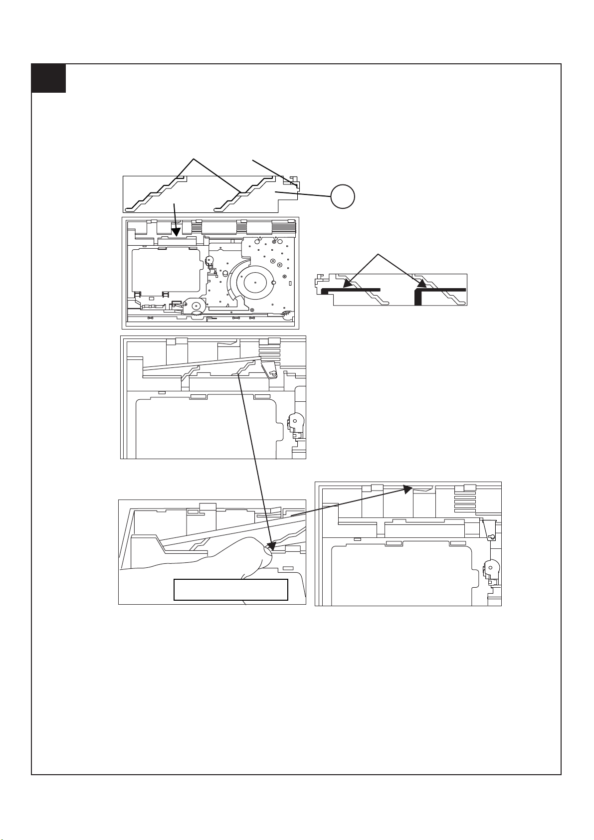
[2] Removing and reinstalling the main parts
CD-DV600W
1. TAPE MECHANISM SECTION
Perform steps 1 to 5 and 6 of the disassembly method to remove the
tape mechanism.
1.1. How to remove the record/playback and erase heads
(TAPE 2) (See Fig. 1)
1. When you remove the screws (A1) x 2 pieces, the recording/playback head and three-dimensional head of the erasing head can be
removed.
TAPE 2
Clutch Assembly
Record/Playback
Head
Erase Head
(A1)x2
φ2x6mm
Figure 1
Pinch
Roller
Pawl
<A>
Pull
<B>
Pinch Roller
(C1)x1
TAPE 2
Pinch Roller
(C1)x1
TAPE 1/TAPE 2
Pull
<B>
<A>
Pinch
Roller
Pawl
Figure 3
1.4. How to remove the belt (TAPE 2) (See Fig. 4)
1. Remove the main belt (D1) x 1 piece, from the motor side.
2. Remove the FF/REW belt (D2) x 1 piece.
1.5. How to remove the belt (TAPE 1) (See Fig. 4)
1. Remove the main belt (E1) x 1 piece, from the motor side.
2. Remove the FF/REW belt (E2) x 1 piece.
Tape
Motor
TAPE 2
Main Belt
(D1)x1
TAPE 1
Main Belt
(E1)x1
TAPE 2
FF/REW
Belt
(D2)x1
Tape
Motor
1.2. How to remove the playback head (TAPE 1)(See Fig. 2)
1. When you remove the screws (B1) x 2 pieces, the playback head
can be removed.
(B1)x2
φ2x9mm
TAPE 1
Clutch Assembly
Playback
Head
Figure 2
1.3. How to remove the pinch roller (TAPE 1/2) (See Fig. 3)
1. Carefully bend the pinch roller pawl in the direction of the arrow
<A>, and remove the pinch roller (C1) x 1 piece, in the direction of
the arrow <B>.
Note:
When installing the pinch roller, pay attention to the spring mounting
position.
TAPE 1
Main Belt
(D1)x1
Main Belt
(E1)x1
FF/REW
Belt
(E2)x1
Figure 4
1.6. How to remove the motor (See Fig. 5)
1. Remove the screws (F1) x 2 pieces, to remove the motor.
Tape
Motor
Clutch Assembly
(F1)x2
φ2.6x5mm
Figure 5
3 – 4
Page 52

CD-DV600W
Mark 1
(DISC 1)
(DISC 2)
(DISC 3)
(DISC 4)
(DISC 5)
Gear up down board
Mark 3 Mark 5
Mark 2 Mark 4
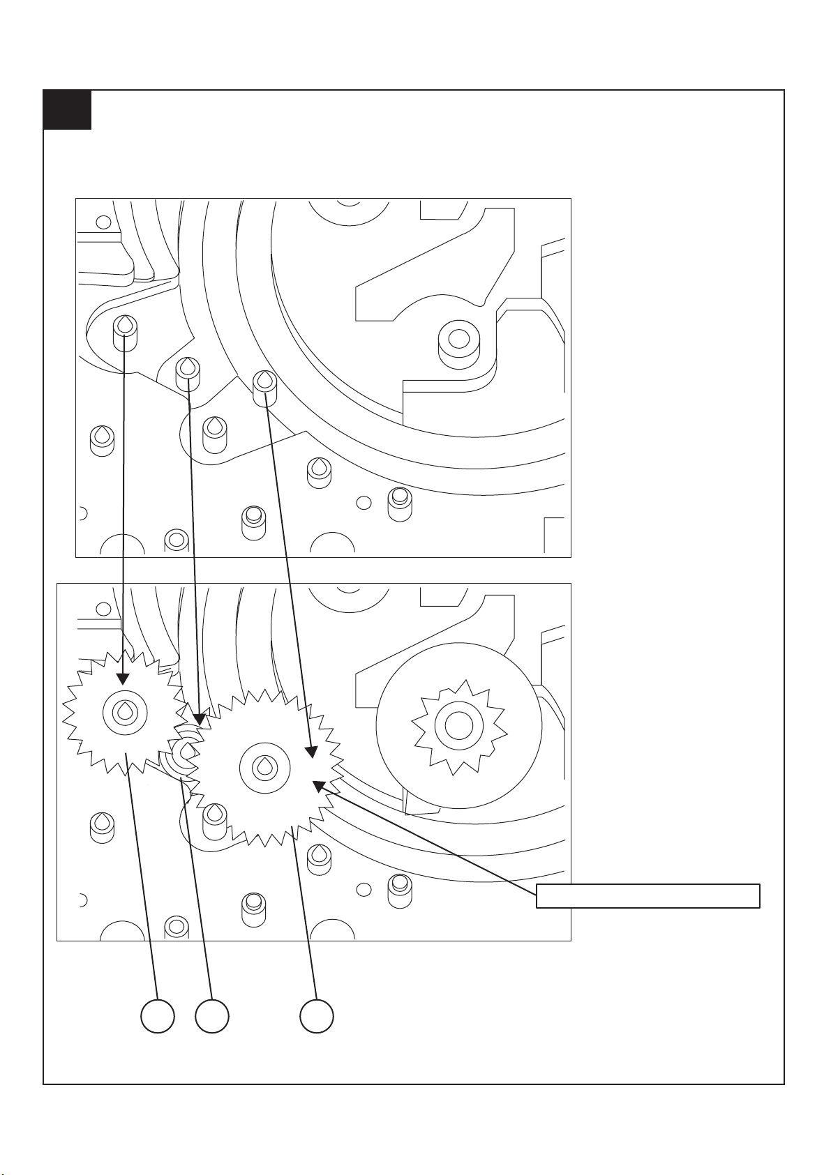
2. CD MECHANISM SECTION
Perform steps 1, 2, 11, 12 and 13 of the disassembly method to
remove the CD mechanism.
2.1. Remove the pickup. (See Fig. 1)
1. Remove the stop washer (A1) x 1 piece, to remove the gear (A2) x
1 piece.
2. Remove the screws (A3) x 2 pieces, to remove the shaft (A4) x 1
piece.
3. Remove the pickup.
Note
After removing the connector for the optical pickup from the connector
wrap the conductive aluminium foil around the front end of connector
so as to protect the optical pickup from electrostatic damage.
(A3)x2
φ2.6x6mm
CD Mechanism
Shaft
(A4)x1
Gear
(A2)x1
Reduction gear C
Front Rear
Figure 3
2. In another case, if CD mechanism is at tray No.1 play position and
to remove CD located in tray No.3, the procedure is as follows:
If the gear up down board is located at tray No.1 position, then
rotate gear clock-wise until it at stock position. Rotate reduction
gear D clockwise (Figure 4) to move the CD mechanism to tray
No.3 position.This is confirmed by checking the gear up down
board position by the marking as indicated on the main chassis as
shown in Figure 5.
Reduction gear D
Stop Washer
(A1)x1
Pickup Unit
Figure 1
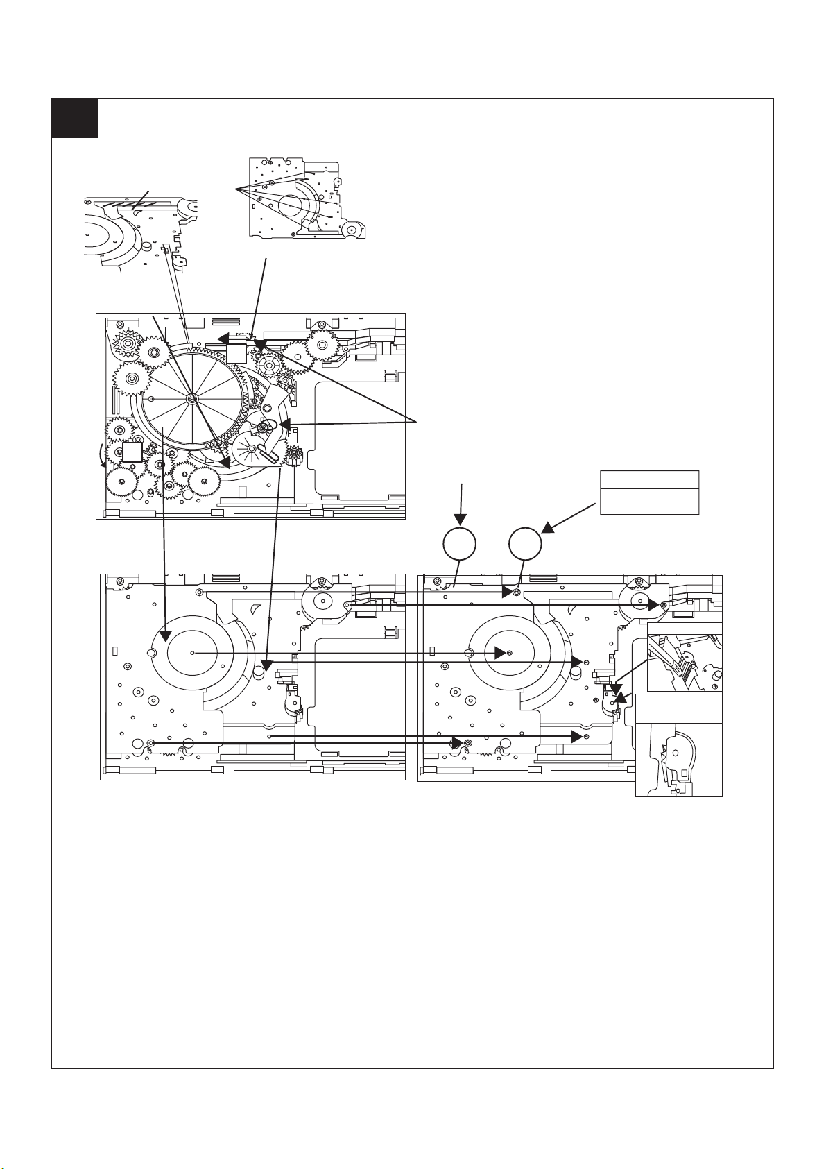
3. CHANGER MECHANISM SECTION
Perform steps 1, 2, 11, 12 and 13 of the disassembly method to
remove the CD changer mechanism.
3.1. How to remove CD Disc (See Fig. 2~5)
1. When CD is at play position (Figure 2), rotate reduction gear C
clock-wise as shown in Figure 3 until disc tray is at stock position,
then rotate further to eject the disc tray so that CD can be removed
from the tray.
CD Disc
Disc Tray
Guide Tray
CD at play position.
CD Disc
Up Down
Figure 4
Figure 5
Figure 2
CD at stalk position.
3 – 5
Page 53

3.2. How to Remove the tray motor/main cam motor/5Changer Motor PWB (See Fig. 6)
1. Remove the screws (A1)x 2 pieces, to remove tray motor/main cam
motor/5-Changer Motor PWB.
Changer Mechanism Unit
CD-DV600W
Main Cam Motor
(A1)x2
φ2x10mm
Figure 6
NOTE: There are 2 more screws tighten the motors at the bottom of
main chassis. Before performing procedure 1 above, disc stop
spring, top plate sear up down board and trays must be
removed, then only the 2 screws can be untighten.
Tray Motor
5-Changer
Motor PWB
3 – 6
Page 54

CD-DV600W
b
R
I
4
C
AudioCD-DV999W/CD-DV777WService ManualCD-DV999W/CD-DV777WMarketE
CHAPTER 4. DIAGRAMS
[1] Block diagrams
D3.3V
A5V
IC501
3
2
1
AUDIO
DIGITAL
OUT
DVD/CD
SO7001
S-VIDEO
OUT
JK7002
VIDEO
OUT
M2
MAIN CAM
MOTOR
M
M
M1
TRAY
MOTOR
FROM MAIN PWB
FROM MAIN PWB
CN3203
14
13
12
11
10
CN3201
10
11
CN3003
10
11
12
13
CN3004
SPDIF
1
DGND
2
3
D3.3V
MUTE
TXD
DGND
RXD
PROGRESSIVE
9
ASPECT
VGND
8
Py_OUT
7
Pb_OUT
6
Pr_OUT
5
VGND
4
V_OUT
3
C_OUT
2
1
CAM-
1
CAM+
2
TR-
3
TR+
4
DVD_CS
5
DVD_CLK
6
SYS_DATA
7
DVD_DATA
8
DVD A_MUTE
9
RESET
RXD_CTL_IN
RÐCH
1
AUDIO_GND
2
LÐCH
3
M_GND
4
A_5V
5
D_GND
6
+8V
7
S_5V
8
S_5V
9
A_GND
D_1.5V
A3.3V
D3.3V
A_5V
+8V
S_5V
D1.5V
A3.3V
D3.3V
Q3100
Q3101
Q3102
IC3003
TC7WT126
BUFFER
D3.3V
D3.3V
IC3503,IC3504
20
TCLV573T
8 bit LATCH IC
5
6
DGNDAUDIO
94
Q3501
D3.3V
131412
14
15
16
13
D3.3V
D3.3V
1,7,8
IC3002
BD4825G
RESET
A0-A15
8
7
IC3801
PCM1748E
D/A CONVERTER
GND
IC3501
IXA173WJ
FLASH ROM
27,46
1,10
Figure 4-1 BLOCK DIAGRAM (1/4)
ADAC_DA
NEXOENEXCENEXWEFADT(0-20)
IECOUT
DAC1OUT
DAC4OUT
DAC5OUT
DVD_CS
S_CLK
S_DIN
S_DOUT
AMUTE
NRST
RXD_CLT_IN
P15(RXD_CLT)
D_3.3V
43,49,55,75,81
1,3,9,15,29,35,41
1,12D3.3V
10
ADAC_CK
ADAC_L
768FS
181
RXD
52
158
163
164
60
53
55
54
94
68
59
47
NRAS
NCSM
IC3401
IX0614AW
64M SD-RAM
D_GND
14
15
IC3601
BU2363FV
CLOCK
GENERATOR
2,11
D_GND
DQM(0-3)
MA(0-11)
MDQ(0-31)
MCK
NWE
NCAS
6,12,32,38,44,46,52
58,72,78,84,86
873
X3601
974817296
BA(0-1)
D_3.3V
IXA46
DVD DE
8
IC30
4K
49,92,170
B
4 – 1
Page 55

3
IC3001
IXA464AW
DVD DECODER
49,92,170
V
BR24L04F
8
4K bit EEPROM
IC3602
1-4,7
104,118,145,149
153,157,165
A3.3V
6
5
63
P2(SDA)
P3(SCL)
FG
SPIN
66
146
106,119,138
151,155,159,167
4,11,16,24,30,43
58,69,80,93,99,169
177,183,194,198,206
211,215,221,224,230
236,241,245,248,254
1,7,14,23,29,42
56,79,91,171,182
189,195,202,209
218,226,233,240,250
15,67,98,186
213,222,244
62
121-131
134,136
VHALF
137
73,71,70
152,150
133,135
LPCO1
LPCO2
CD-DV600W
FG
7
5,6
VCC
S_5V
SPIN
31-34
VHALF
VCC
M_8V
A_GND
D_GND
D3.3V
D1.5V
74
Q3305
Q3306
Q3303
Q3304
D3301
A_GND
25
SPIN/SLED DRIVER
9,27,28
14
29
A_GND
IC3702
NJM12904
8
OPE.AMP.
1
IC3704
LA6261
FOCUS/TRACKING
18
12
16
S_5V
IC3301
7SB3157P
ANALOG
SWITCH
Q3307
DVD_H
35,36
2,3
3,4
7,26
1,2
M_GND
L
H
S_5V
PD_CD
4
5,6
A_GND
SPIN-
SPIN+
CN3301
1
2
3
4
5
6
7
8
9
10
11
12
13
14
15
16
17
18
19
20
21
22
23
24
A_3.3V
GND
LD_DVD
NC
VOSC
PDMON
LD(CD)
VR(DVD)
VR(CD)
NC
VE
VCC
Vref
G(PDIC)
VF
VB
VA
RF
CD/DVD
VD
VC
TR-
TR+
FO+
FO-
D_GND
DVD MECHANISM
UNIT ASS'Y
SPIN-
SPIN+
IN SW
SL-
SL+
AGND
FG
LED
M
SPINDLE
MOTOR
M
SENSOR
PWB
PICKUP
SLED
MOTOR
UNIT ASSY
Figure 4-2 BLOCK DIAGRAM (2/4)
4 – 2
Page 56

CD-DV600W
V
E
L
V
E
D
FM
ANTENNA
S0302
BF301
B. P. F.
AM LOOP
ANTENNA
1
2
CNP301
ICK1
M65856SP
MIC AMP
JK1
MIC
JK2
MIC
VRK1
MIC
LEVEL
FROM CD SECTION
CNP7
REC / P.B. HEAD
L–CH
TA P E
R–CH
AC BIAS
1
FM FRONT END
34 5 7 8
FM
L312 T312
RF
AM TRACKING
T303
40
LATCH
42
DATA
41
CLOCK
9
ROUT
35
36
LOUT
4
RIN
32
31
LIN
12
13
VCC
23
22
QK1
1
2
3
BI601
SWITCHING
Q101–
Q104
IC301
TA7358AP
T306
+B4
L(TA)
R(TA)
L REC
R REC
VT
FM OSC
OSC BUFF
Q302
AM BAND
COVERAGE
6
5
2
3
2
23
REC
9
16
11
12
NOR/
15
HIGH
6
9
FM IF
T302
IC303
LA1832S
FM IF DET./
FM MPX./AM IF
VT
+B5
+B
FM
Q360
ICK2
KIA4558P
OPE AMP
7
1
JK691
13
P. B .
L
4
R
21
H/N
L
7
R
18
IC101
AN7345K
PLAYBACK AND RECORD/
PLAYBACK AMP.
FM IF
CF 303
4.5 MHz
20
1
FM
SWITCHING
JK690
L
R
+B5
PB
REC
450 kHz
T351
CF352
AM IF
1
24
AM MIX
OUT
23 21 24
AM OSC IN
X352
22
OSC
7 9
VIDEO/AUX
AUX
TUNER
15 16 11
PLL (TUNER)
TAPE
CD
AM RF IN
AM OSC OUT
IC302
LC72131
L
R
L
R
L
R
L
R
7
STEREO
MO/STFM/AM
10 21
9
16
10
15
11
14
12
13
10.7 MHz
CF351
598
AM IF GND FM+B FM
DET
FM/AM
MPXIN
OUT FM/AM
18 16 12
CEIDCLK
DO
3 4 5 6
8
17
IC601
LC75341
AUDIO PROCESSOR
7
18 23
Q107
Q108
MUTING
X351
456 KHZ
17 13
VCO
MO/ST
17
4
ZD351
L
14
R
15
DI
CE
CLK
24
21
+B5
REC/PLAY
5.1 V
1
2
4
+B5
–20dB
AT T
R
L
7
NJM2533
Q601
Q602
IC602
VIDEO
SWITCH
Q603
Q604
SYSTEM
MUTE
3
ERASE
HEAD
SWITCHING
Q105
Q106
Q112
Q114
+B5
SWITCHING
SWITCHING
Q113
+B5
BIAS
OSC
Q111
L103
Q109 Q110
SWITCHING
Figure 4-3 BLOCK DIAGRAM (3/4)
4 – 3
BIAS
BIAS
+B3
+B3
MOTOR
DRIVER
Q706
Q711
Q712
Q707
Q708
Q714
–
Q717
SOLENOID
DRIVER
DVD 1. 7 V
TA P E
MECHANISM
ASS'Y
DVD 3. 7 V
R
2
R
2
L
Page 57

1 2
FL701
FL DISPLAY
+B10
4441323128215 45
TAPE
MECHANISM
ASS'Y
CD-DV600W
SYSTEM
MUTE
3
4
JOG701
VOLUME
L
1
R
15 14
2
69
78
VLOAD
79
8
9
80
83
84
100
1 2
SP DET
+B10
IC901
STK432–070
POWER AMPS
7
L – OUT
R – OUT
GND
10
–VCC
+VCC
13
9
8
4A 250V
38 43 44 40
46
VDD
IC701
IXA032AWZZQ
SYSTEM MICROCOMPUTER
VDD
F802
T_BIAS
T_REC/PLAY
3 4 47
Q901–
Q904
SP_RLY
RESET
10 6
7 11 12 15 16 21 24 17 18 19 20
XL700
4.1943 MHz
+B10
Q709
RESET
VDD
+B10
Q905
RL914
25 13
CLKDIDO
AVD D
CE
DRIVER
Q906
+B3
39
+B10
34
33
31
27
SMUTE
41
+B4 (8V)
FAN MOTOR
M4
M
SO901
SPEAKER TERMINAL
JK701
HEADPHONE
REMOCON SENSOR
31
SW701 – SW707
SW712 – SW716
SW725 – SW735
+5V
+B7 (A_5V)
RX701
2
KEY
TO DVD SECTION
+B10
SW601
SPAN
SELECTOR
D1.7V
E
NISM
'Y
D3.7V
VF1
–VF1
VF2
VOLTAGE
REGULATOR
IC856
2
LD1117V
VOLTAGE
REGULATOR
IC855
2
LD1117V33
F801
IC851
AN80T53
10 V
8.5 V
5.1V
GND
1
+B7 (A_5V)
+B8 (D_5V)
1
VCCSW13 V
4
3
D871 D870
5
2
+B3
6
7
+B4
2
3
4A 250V
2A 250V
2A 250V
VOLTAGE
REGULATOR
Q801
IC853
BD9701T
CONVERTER
F804
F803
PT801
POWER
TRANSFORMER
T. F.
IC852
11 33
KIA7808AP
LD+8 V
UNSW_5.6 V
VOLTAGE REGULATORVOLTAGE REGULATOR1-CH DC–DC
IC854
AN78L05
L841
AC POWER
SUPPLY CORD
AC 220–240V
50Hz/60Hz
1
Figure 4-4 BLOCK DIAGRAM (4/4)
4 – 4
Page 58

CD-DV600W
AudioCD-DV999W/CD-DV777WService ManualCD-DV999W/CD-DV777WMarketE
CHAPTER 5. CIRCUIT DESCRIPTION
[1] Notes on schematic diagram
•Resistor:
To differentiate the units of resistors, such symbol as K and M are
used: the symbol K means 1000 ohm and the symbol M means
1000 kohm and the resistor without any symbol is ohm-type resistor. Besides, the one with “Fusible” is a fuse type.
• Capacitor:
To indicate the unit of capacitor, a symbol P is used: this symbol P
means pico-farad and the unit of the capacitor without such a symbol is microfarad. As to electrolytic capacitor, the expression
“capacitance/withstand voltage” is used.
(CH), (TH), (RH), (UJ): Temperature compensation
(ML): Mylar type
(P.P.): Polypropylene type
• Schematic diagram and Wiring Side of P.W.Board for this model are
subject to change for improvement without prior notice.
• The indicated voltage in each section is the one measured by Digital Multimeter between such a section and the chassis with no signal given.
1. In the tuner section,
indicates AM
indicates FM stereo
2. In the main section, a tape is being played back.
3. In the deck section, a tape is being played back.
( ) indicates the record state.
4. In the power section, a tape is being played back.
5. In the CD section, the CD is stopped.
• Parts marked with “ “ ( ) are important for maintaining the safety of the set. Be sure to replace these parts with
specified ones for maintaining the safety and performance of the
set.
REF. NO DESCRIPTION POSITION
JOG701 VOLUME ON—OFF
NSW1 PICKUP IN ON—OFF
SW1 CLAMP ON—OFF
SW2 TRAY SW1 ON—OFF
SW3 TRAY SW2 ON—OFF
SW4 DISC ON—OFF
SW601 SPAN SELECTOR 100 kHz/
SW701 POWER ON/STAND-BY ON—OFF
SW702 CLOCK/TIMER ON—OFF
SW703 TUNING UP ON—OFF
SW704 TUNING DOWN ON—OFF
SW705 FAST REWIND/PRESET DOWN ON—OFF
SW706 EQUALIZER ON—OFF
SW707 FAST FORWARD/PRESET UP ON—OFF
10 kHz
[2] Types of transistor and LED
FRONT
VIEW
ECB
(S)(G)(D)
(1)(2)(3)
KRC107 M
KTA1266 GR
KTA1273 Y
KTA1274 Y
KTC3194 Y
KTC3199 GR
KTC3200 GR
KTC3203 Y
B
(1)
(3)
E
TOP
VIEW
KRA107 S
KRC102 S
KRC104 S
KTA1504 Y
KTC3875 GR
2SB709 AR
2SD601 AR
KTC3265 Y
(2)
REF. NO DESCRIPTION POSITION
SW712 TUNER (BAND) ON—OFF
SW713 CD ON—OFF
SW714 TAPE ON—OFF
SW715 GAME/VIDEO ON—OFF
SW725 PLAY/REPEAT ON—OFF
SW726 STOP ON—OFF
SW727 REC/PAUSE ON—OFF
SW728 MEMORY/SET ON—OFF
SW729 OPEN/CLOSE ON—OFF
SW730 DIRECT PLAY ON—OFF
SW731 DISC2 ON—OFF
SW732 DISC4 ON—OFF
SW733 DISC5 ON—OFF
SW734 DISC3 ON—OFF
SW735 DISC1 ON—OFF
SW716 X-BASS / DEMO ON—OFF
TOP VIEWTOP VIEW
C
FRONT
VIEW
1N4148
1N4004S
DS1SS133
304VT2H3
FRONT
VIEW
5 – 1
AC AC
D5SBA60F
Page 59

[3] Waveforms of DVD circuit
CD-DV600W
2003/10/16 13:19:45
Stopped
DVD_CS IN1
S_DIN2
Normal
20 MS/s 50 µs/div786
CH1 10:1
0.500 V/div
DC 10kHz
CH2 10:1
0.500 V/div
DC Full
CH3 10:1
0.500 V/div
DC Full
CH4 10:1
0.500 V/div
DC Full
S_DOUT3
Edge CH1
Auto
0.400 V
SCLK OUT4
SIMPLE
Level
1.000 V
5 – 2
Page 60

CD-DV600W
[4] Voltage
PIN
NO.
10
11
12
13
14
15
16
17
18
19
20
21
22
23
24
25
26
27
28
29
30
31
32
33
34
35
36
37
38
39
40
41
42
43
44
45
46
47
48
49
50
51
52
53
54
55
56
57
58
59
60
61
62
63
64
65
66
67
68
69
70
71
72
73
74
75
76
77
78
79
80
1
2
3
4
5
6
7
8
9
IC1
VOLTAGE
3.20 V
1.61V
1.61 V
1.60 V
1.61 V
3.08 V
1.65 V
1.65 V
1.65 V
1.65 V
1.48 V
0V
1.65 V
0V
1.65 V
1.47 V
1.48 V
0V
0V
0V
1.60 V
0V
1.61 V
1.61 V
0V
0V
3.20 V
0V
3.20 V
0V
0V
1.59 V
1.60 V
3.20 V
0V
0V
0V
0V
0V
0V
3.61 V
0V
0V
1.80 V
3.60 V
0V
1.45 V
1.49 V
3.19 V
3.79 V
0V
0V
0V
0V
0V
0V
0V
0V
0V
3.20 V
0V
0V
0.63 V
0V
5.16 V
5.18 V
4.68 V
0V
0V
0V
0V
0V
0V
4.86 V
4.86 V
3.01 V
0V
1.12 V
0V
3.20 V
PIN
NO.
10
11
12
13
14
15
16
17
18
19
20
21
22
23
24
25
26
27
28
29
30
31
32
33
34
35
36
PIN
NO.
10
11
12
13
14
15
16
17
18
19
20
21
22
23
24
1
2
3
4
5
6
7
8
9
1
2
3
4
5
6
7
8
9
IC2
VOLTAGE
2.10 V
2.20 V
2.10 V
2.20 V
2.10 V
2.20 V
0V
4.37 V
5.02 V
3.20 V
1.62 V
1.65 V
1.62 V
1.65 V
1.62 V
0V
1.62 V
1.64 V
4.71 V
4.71 V
3.92 V
3.11 V
3.10 V
2.50 V
1.65 V
0V
5.02 V
8.68 V
5.02 V
0.59 V
0.71 V
0V
0V
0V
2.11 V
2.20 V
IC101
VOLTAGE
0V
0V
0.57 V
2.03 V
0.44 V
0V
0V
0.58 V
3.45 V
3.35 V
0V
0V
6.97 V
4.16 V
0V
3.42 V
0.57 V
0V
0V
0.41 V
2.03 V
0.57 V
0V
0V
PIN
NO.
PIN
NO.
10
11
12
13
14
15
16
17
18
19
20
21
22
PIN
NO.
10
11
12
13
14
15
16
17
18
19
20
21
22
23
24
1
2
3
4
5
6
7
8
9
1
2
3
4
5
6
7
8
9
1
2
3
4
5
6
7
8
9
IC301
VOLTAGE
0V
0V
0.29 V
0.20 V
0V
0.29 V
0.26 V
0.29 V
0.29 V
IC302
VOLTAGE
2.57 V
0V
0V
0V
0V
5.22 V
10.18 V
4.76 V
0V
0V
5.23 V
0V
5.23 V
0V
0V
2.59 V
5.24 V
0V
0V
10.18 V
0V
2.57 V
IC303
VOLTAGE
1.97 V
5.15 V
1.97 V
1.96 V
0V
0V
5.21 V
3.59 V
5.15 V
0V
2.01 V
1.25 V
2.27 V
1.13 V
1.10 V
1.96 V
0V
1.29 V
2.08 V
1.29 V
1.95 V
1.95 V
5.15 V
3.65 V
PIN
NO.
10
11
12
13
14
15
16
17
18
19
20
21
22
23
24
PIN
NO.
PIN
NO.
PIN
NO.
PIN
NO.
1
2
3
4
5
6
7
8
9
1
2
3
4
5
6
7
1
2
3
1
2
3
1
2
3
IC601
VOLTAGE
0V
0V
0V
5.10 V
5.10 V
5.10 V
5.10 V
5.11 V
5.10 V
5.10 V
5.10 V
5.10 V
5.10 V
5.10 V
5.10 V
5.10 V
5.10V
5.10 V
5.10 V
5.10 V
5.10 V
5.10 V
10.20 V
0V
IC851
VOLTAGE
5.22 V
13.11 V
20.66 V
0V
19.72 V
10.22 V
8.67 V
IC852
VOLTAGE
20.23 V
0V
7.96 V
IC855
VOLTAGE
1.411 V
0.817 V
0V
IC856
VOLTAGE
0.579 V
0V
0V
PIN
NO.
10
11
12
13
14
15
16
17
18
19
20
21
22
23
24
25
26
27
28
29
30
31
32
33
34
35
36
37
38
39
40
41
42
43
44
45
46
47
48
49
50
1
2
3
4
5
6
7
8
9
VOLTAGE
4.74 V
4.65 V
0V
4.70 V
4.72V
4.72 V
0V
0V
0V
4.83 V
2.27 V
1.99 V
0V
4.73 V
0V
4.74 V
0V
0V
5.22 V
0V
0V
4.68 V
0V
0V
0V
5.20 V
0V
5.01 V
5.01 V
2.64 V
5.01 V
5.01 V
0V
0V
5.01 V
1.67 V
5.20 V
5.01 V
4.87 V
0V
2.02 V
0V
13.10 V
0V
0V
4.74 V
0V
4.61 V
0V
0V
IC701
PIN
NO.
51
52
53
54
55
56
57
58
59
60
61
62
63
64
65
66
67
68
69
70
71
72
73
74
75
76
77
78
79
80
81
82
83
84
85
86
87
88
89
90
91
92
93
94
95
96
97
98
99
100
PIN
NO.
1
2
3
4
5
6
7
8
9
10
11
12
13
14
15
VOLTAGE
0V
0V
0V
0V
5.17 V
5.17 V
-29.70 V
0V
-0.26 V
-0.24 V
-0.22 V
-0.20 V
-0.19 V
-0.19 V
-0.18 V
-0.17 V
-0.16 V
0V
-29.90 V
-29.90 V
-29.90 V
-29.90 V
-29.90 V
-19.76 V
-27.40 V
-24.87 V
-22.29 V
-22.30 V
-30.13 V
-27.43 V
-14.50 V
-27.20 V
-19.30 V
-6.08 V
-21.85 V
-27.22 V
-21.89 V
-17.00 V
-27.38 V
-27.10 V
-27.07 V
-27.00 V
-27.00 V
-27.35 V
-26.27 V
-27.11 V
-27.00 V
-27.07 V
-27.07 V
-26.83 V
IC901
VOLTAGE
-0.150 V
-0.150 V
0V
38.13 V
-36.67 V
0V
0V
39.27 V
-39.25 V
0V
0V
-37.93 V
0V
-0.150 V
-0.144 V
5 – 3
Page 61

-MEMO-
CD-DV600W
5 – 4
Page 62

CD-DV600W
A
B
C
D
E
F
G
H
1
23456
DVD SIGNALFM SIGNAL
PLAYBACK SIGNAL
RECORD SIGNAL
VIDEO SIGNAL
AUX SIGNAL
MIC SIGNAL
BI601
2715AWZZ
R619
330
R618
330
Q605
R665
4.7K
1/50
1/50
R680
R681
C671
C670
10K
10K
DVD R -CH
DVDA_GND
V MDL: A_10V
U/H/W MDL: A_5V
DVD L -CH
DVDM_GND
DVDA+5V
DVDD_GND
LD + 8V
DVD S 5V
DVD S 5V
DVDA GND
DVD D 1.7 V
DVD D 3.7 V
DVDA3.7V
DVD I N
LD+8V
A_5V
CD+5V
CD_GND
A_GND
CD_D_GND
CD_A_GND
AC RLY
DVD S 5V
DVD S 5V
DVD_FUNC
DVD P ROTE CT
DVD D 1.7 V
L-CH
R-CH
1
2
3
4
5
6
7
8
9
10
11
12
13
14
1
2
3
4
5
6
7
8
9
10
11
12
13
14
15
TO POWE R SECTIO N
TO DVD SERVO
2.2K
R666
KTC3875SGR
10KHZ/100KHZ
9KHZ/50KHZ
S0024AW
SW601
PLAYBACKHEAD
TAP E 1
1187AW
CNS101
R-CH
L-CH
3
2
1
CNP101
M705C
C102
560P
C101
560P
ERASE
M_GND
T2-R2
A_GND
T2_R1
T2_L1
T2_L2
CNP102
1188AW
CNS102
TAPE2
RECORD/
PLAYBACKHEAD
ERASE HEAD
6
5
4
3
2
1
L-CH
R-CH
CNP102
M705G
1
2
3
1
2
3
4
5
6
7
1
2
3
4
5
6
7
C103
180P
0V
0V
0V
SWITCHING
C3200GR
Q103
0.7V
R105
3.3K
0.7V
R103
2.2K
Q101
C3200GR
SWITCHING
0V
0V
0V
SWITCHING
C3200GR
Q102
0.7V
0.7V
R104
2.2K
R106
Q104
C3200GR
SWITCHING
108P
C104
3.3K
R109
4.7K
R107
47K
0V
0V
0V
Q105
KTC3875SGR
SWITCHING
C105
1500P
0V
0V
0V
R110
4.7K
R108
47K
1500P
C106
Q106
KTC3875SGR
SWITCHING
R101
1K
R102
R112
15K
Q112
KTA1504SGR
1K
9.3V
9.3V
R146
10K
8.6V
L
R148
4.7K
R147
10K
SWITCHING
Q113
KRC104S
3.4V
0V
0V
0V
3.4V
Q114
KRC104S
SWITCHING
R116
56
C116
560P
R120
3.9K
R118
100K
C114
0.039
C112
47/25
C110
330P
R114
1K
C108
330P
R
L
330P
C107
R113
1K
C109
330P
R117
100K
C113
0.039
C111
47/25
R115
56
C115
560P
R119
3.9K
C117
47/25
R123
10K
R121
15K
C119
C121 0.022
3.3/50
C143
4.7K
R127
R131
0.022
R133
100
3300P
C129
C131
47/25
R135
10K
1.5K
C.127
R129
5.6K
C123
270P
2200P
R111 15K
C125
22/50
112K
56K
56K
112K
Hich=T1
IC101
AN7345K
Hich=CHROME
ALC
ALC
Nor/Cr02
RIPPLE
Vcc
C118
47/25
47/50
R124
10K
R122
R126
15K
C120
C150
2200P
68K
R150
4.7K
C124
270P
R128
5.6K
R130 1.5K
R132
C128
0.022
C126
22/50
R158
220
100
C130 3300P
C132
47/25
R134
10K
C133
22/25
C134
220/10
C135
0.022
R
0V
Q108
KTC3875SGR
MUTING
R138
10K
0.7V
R139
10K
REC_R
0.7V
Q107
KTC3875SGR
MUTING
R136
220K
R137
220K
0V
REC_L
R149
150
(1/4W)
C141
100/16
(1/4W)
Q1
KTA
R142
0V
82
1/2W
R143
R144
C137
0.047
47K
22K
0V
8200P
C138
C139
0 039
5.6K
5.6K
SP
C
1
C
1
KTC3875SGR
Q606
R667
4.7K
R668
2.2K
C632
1000P
SPARE
SP
3300P
C612
R606
4.7K
1/50
4.7/50
1/50
1/50
1/50
1/50
C614
C616
C618
C620
C622
C624
0.1 (ML)
0.1 (ML)
C606
C608
220/10
C603
R656
10K
C
C
1
R604
10K
C610
1/50
R603
1K
C602
0.022
C601
220/16
C653
220P
R608
R609
C626
2200P
C625
2200P
IC601
LC75341
AUDIOPROCESSOR
CLK
VDD
VREF
ROUT
RBASS
RTRE
RIN
RSELO
R4
R3
R2
R1
DI
CE
VSS
LOUT
LBASS
LTRE
LIN
LSELO
L4
L3
L2
L1
AUX
DECK
TUNER
CD
CCB
INTERFACE
C605
0.1
(ML)
C607
0.1
(ML)
C611
3300P
C613
1/50
C615
4.7/50
C617
C619
1/50
1/50
C621
1/50
C623
1/50
C633
1000P
SPARE
C631
1000P
SPARE
1000P
C629
SPARE
C627
1000P
R607
4.7K
C609
1/50
R605
10K
C657
470P
R657
10K
R621
22K
C639
1/50
R621
C640
22/50
R612
390
Q602
KTC3875SGR
R610
2.2K
C636
1000P
C635
1000P
2.2K
R611
R613
390
Q601
KTC3875SGR
R614
R615
3.9K
3.9K
Q602
KTC3875SGR
2.2K
R616
C638
1000P
C637
1000P
2.2K
R617
Q603
KTC3875SGR
22K
R601 1K
R602 1K
C651
220P
C652
220P
12 4 5 6 7 8 91011123
1
2
4
5
6
7
8
9
10
11
12
3
24 23 21 20 19 18 17 16 15 14 1322
24
23
21
20
19
18
17
16
15
14
13
22
1
2
3
4
5
6
7
8
9
10
11
12
14
15
16
ONLY
W/V
T1_R
A_GND
T1_L
SPANSELECTOR
*NOTE ON SCHEMATIC DIAGRAM can be found on page 5-1.
AudioCD-DV999W/CD-DV777WService ManualCD-DV999W/CD-DV777WMarketE
CHAPTER 6. CIRCUIT SCHEMATICS AND PARTS LAYOUT
[1] Schematic diagram
Figure 6-1 SCHEMATIC DIAGRAM (1/15)
6 – 1
Page 63

CD-DV600W
C130 3300P
C
C601
220/16
C603
220/10
C608
0.1 (ML)
C606
0.1 (ML)
C612
614
1/50
616
4.7/50
618
1/50
620
1/50
622
1/50
624
1/50
R668
5.6K
R608
2200P
REC_R
R139
10K
Q107
KTC3875SGR
MUTING
10K
R134
C132
47/25
22/25
C133
16 15 14 13
RIPPLE
Nor/Cr02
ALC
ALC
9101112
C131
47/25
R135
10K
2.2K
220/10
C134
BI603
2714AW
220
470/10
0.01
C7001
47/10
5
4
3
2
1
1
2
3
4
5
R669
220
R664
R7003
C7011
1
2
3
OPT OUT
0
R7002
47P
0
R7001
1
2
3
4
5
6
5
4
3
2
1
0
WTM901
019EAW
C669
100/16
1000/6.3
0
C7005
GAME INPUT PWB
R691
6.8K
R690
6.8K
C667
R677
CNP7002
C7004
4
3
2
1
5
C7002
0.022
IC501
TX141
2.2K
C7003
C
1
2
47P
C691
390P
C690
390P
VMDL:1
VIDEO OUT
47P
S-VIDEO
S07001
D0401AW
A+10V
DGND
TUN_R
AGND
TUN_L
TUN_SM
J0110AW
JK7002
Y
JK692
M0004AW
HEADPHONES
6
VIDEO IN
5
R693
4
Lch
47K
3
R50
R692
47K
CE
AUX/VIDEO
2
0
1
Rch
JK690
JO313AW
R688
GAME VIDEO INPUT
CHASSIS
29
30
31
DI
32
CLK
33
34
35
TOTUNER SECTION
36
DO
37
38
22
DISCTYPE
21
DVD P ROTE CT
DVDFUNC
20
TUN SM/SPAN
19
MIC
18
KARAOKE
17
CE
16
DO
15
CLK
14
13
DI
+B_PROTECT
12
11
D_GND
S_MUTE
10
9
T_T1/T2
REC/PLAY
8
T_BIAS
7
A+10V
6
M_+13V
5
SW_5V
4
3
SP_DET
2
SP_RLY
1
-20dB
CNP701B
ZX21AW
TO DISPLAYSECTION
KOK OU T(L)
KOK IN (L)
A_GND
A_+10V
KOK OU T(R)
KOK IN (R)
D_GNDDICLK
KOK LATCH
KOK IN (R)
DVDD3.7V
MIC IN
7
11
8
10
9
KARAOKE SECTION
12
910
8
11
7
JK691
1
J0120AW
VIDEO OUT
JP660
0
R673
D _GND
0
1K
R678
R672
1K
SPARE
C662
1
10/16
2
C663
3
IC602
10/16
1K
4
R660
VIDEO
SWITCH
390R670
R671
1K
SPARE
PROGRESSIVE
CNS7001
TO DVD SECTION
+B_PROTECT
M_+13
SW_5V
SP_DET
SP_RLY
NJM2533
VMUTE
DGND
ASPECT
VGND
PY-OUT
PB-OUT
PR-OUT
VGND
COUT
VOUT
D3.3V
D-GND
D_OUT
47
R679
330
C668
R688
8
C664
R676
7
0
100/16
6
5
0.01
C666
10/16
C665
1
TXD
2
3
RXD
4
5
6
7
8
9
10
11
YOUT
12
13
14
3
2
1
FW901
2711AW
M_+13V
SP_RLY
Rch
GND
Lch
2
5
4
3
2
1
CNP603
5P53253
100
2.2K
R662
R661
KTC3265Y
R674
Q661
220
3.3K
R663
R675
JP661
0
DIGITAL / V-OUT PWB
470/10
C7009
CNP7001
8P53253
TXD
1
DGND
2
RXD
3
VGND
4
VGND
5
YOUT
6
COUT
R7008
7
VOUT
8
3
L7001
2
10µH
1
CNP7003
CONE3P53253
3
2
TAPE_A_GND
KOK IN (L)
4
5
AGND
A+10V
6
6
KOKOUT (R)
DVDA3.7V
TO POWER SECTION
1
12345
BIK1
2721AWZZ
C602
0.022
R603
1K
C656
10K
R656
C610
1/50
4.7K
R606
3300P
C632
1000P
SPARE
KTC3875SGR
R137
220K
R136
220K
0.7V
0V
0.022
C135
Vcc
470P
R604
10K
C628
R158
220
R667
REC_L
1000P
SPARE
C630
1000P
C634
1000P
SPARE
R644
5.6K
R643
5.6K
Q606
4.7K
(1/4W)
11.6V
R140
47K
R141
4.7K
Q109
0V
KTA1504SGR
82
1/2W
R142
0V
47K
Q111
R143
0V
KTC3203Y
0V
22K
R144
R145
4.7
(ML)
C137
0.047
8200P
/100
C138
L103
330µH
C139
0.039
KOKOUT (L)
R642
5.6K
R641
5.6K
KRC104S
Q110
47/25
M_GND
17 18 19 20 212224 2523 2726 28
C140
6
7
89101112
Figure 6-2 SCHEMATIC DIAGRAM (2/15)
6 – 2
Page 64

CD-DV600W
A
B
C
D
E
F
G
H
1
23456
M
M
11
1
1
1
2
3
4
5
6
7
8
9
10
11
11
+
+
-
-
TRAY
MOTOR
MAIN CAM
MOTOR
5-CHANGER
MOTOR PWB-E
CNP6A
SW4 DISC
SW1 CLAMP
SW2 TRAY SW1
SW3 TRAY SW2
RX1
M1
M2
FFC7081
FFC703
CN3704
P6-14 11-B
TO
DVD SERVO
PWB
6
1
22
1
CNP701B
P6-2 11-G
TO MAIN PWB
FFC701
*NOTES ON SCHEMATIC DIAGRAM can be found on page 5-1.
111098 7654321
111098 7654321
+5V
+5V
GND
GND
TRAY
SW2
TRAY
SW1
GAM+
TR +
TR -
GAM-
CNP7082
WZX14AWZZ
R7082
47K
R7081
390
FROM DVD SECTION
CNP7083
WYP11AWZZ
CN3003
DVD C S
DVD C LK
DVD S YSD ATA
DVD D ATA
DVD AMUTE
SUB PWB
DVD R ESE T
RXD_CNTIN
PHOTO
PHOTO
CLAMP
CLAMP
DISC
DISC
TRAY SW2
TRAY SW1
FROM DISPLAY SECTION
TO PICKUP SECTION
CNP704
CNP7081
WZY11AWZZ
CAM-
DVD
CS
DVD
CLK
DVD
DATA
DVD
AMUTE
RXD_
CNTIN
SYS
DATA
CAM+
TR -
TR +
RESET
14 13 12 11 10 9 8 7 654321
1
2
3
4
5
6
7
8
9
10
11
1
2
3
4
5
6
7
8
9
10
11
6
5
4
3
2
1
3
2
1
6
5
4
9
8
7
12
11
10
15
14
13
18
17
16
21
22
20
19
1
2
3
4
5
6
7
7
6
5
4
3
2
1
14 13 12 11 10 9 8 7 6 5 4 3 2 1
80
79
78
77
76
75
74
73
72
71
70
69
68
67
66
65
64
63
62
61
60
59
58
57
56
55
54
53
52
51
50 49 48 47 46 45 44 43 42 41 40 39 38 37 36 35 34 33 32
81 82 83 84 85 86 87 88 89 91 92 93 94 95 96 97 98 9990
45 44 43 42 41 40 39 38 37 36
35 34 33
32 31 30 29 28 27 26 25 24 23 22
21 20 19 18 17 16 15 14 13 12 11
47K
R750
R586 0
R587 0
R770 5.6k
M_+13V
R771
4. 7k
R593
10K
R776
10K
R588
SP_RLY
VDD
VSS
T_SOL_A
T_MOTOR
T_SOL_B
TIMER LED
S MUTE
SP DET
PHOTO
AVREF
AVDD
P_IN
REMOCON
10K
R780
0
C710
1000P
1000P
0
R785
R709
R775
4.7K
R794
1.5 (1/4W)
F2
F2
S9S8S7S6S5S4S3S2S1
G11
G10
G9G8G7G6G5G4G3
G2
P20
P19
P18
P17
P16
P15
P14
P13
P12
P11
P10
P09
P08
P07
P06
G11
G10
G09
G08
G07
P05
P04
P03
P02
P01
NP
NP
NXNXNXNXNX
NX
CNP703
D704
S11
S10
S12
VLOAD
S13
S14
S15
S16
(DIST 3). S17
(DIST 2). S18
(DIST 1). S19
(DIST 0). S20
MIC SW
TRAY SW1
TRAY SW2
DISC_SW
MO SPEED
DISC TYPE
VIDEO MUTE
MOT A+
IC701
IXA032A
SYSTEM
MICROCOMPUTER
MOT A -
MOT B+
MOT B -
FUNC DVD
KARA_LATCH
DIST
CLAMP SW
T_FP
PROT
A
DVD_D
SYS_D
DVD_
DVD
V
DVDAM
DVD RE
RXD_CNT
T_T1
VPP
T_REC / P
T_B
-20dB
VJ
VJ
X
V
RE
TUN_SM(SP
T_RUN P
DVD+B
C707
1/50
D701
R574
R757
MO SPEED
MOT B-
MOT B+
MOT A+
MOT A-
VIDEO MUTE
DISC TYPE
DVD PROTECT
DVD FUNC
SPAN/TUNSM/SPAN
MIC
KOK LTCH
+B_PROTECT
CE
DO
CLK
DI
D_GND
S_MUTE
T_T1/T2
REC/PLAY
T_BIAS
M_+13V
SW_5V
SP_DET
SP_RLY
- 20dB
CNP701A
KRA107S
Q717
KRC104S
Q716
KRA107S
Q715
D716
IN4148
KRC104S
KRA107S
Q711
KRC104S
Q712
JOG701
ZA001AW
Q714
J718 0
J701 0
LED701
304VT2E1
R768
10K
R767
10K
R761
10K
KE
Y0
KE
Y1
R
7
19
1
K
R
7
2
0
1
K
R
7
2
1
1K
R
7
36
1
K
R7
33 1K
R7
2
4
1
K
R7
2
95
6
0
R7
2
5
1
K
R7
2
6
2
.2K
R7
2
768
0
R7
2
868
0
R7
3
1
1
0
K
R766
10K
Q706
U : ZY16AW
H/W/V : ZY24AW
U/H: ZY07AW
CNP702A
ZY07AWZZ
MTR
SOL
SOL
SOL2
SOL1
SPARE
+MTR
RUN
RUNT2
T1
R790
Q708
Q707
R778
10K
R777
10K
R779
10K
KTA1273Y
KTA1273Y
KTA1273Y
R787
R786
GND
D710
1N4148
C712
47/25
D709
1N4148
F_REC
8. 2K
4. 7K
4. 7K
CNP702A
ZYO7AWZZ
W/V/DVD: ZY09AW
R748
R576
R577
R578
R579
R744
R743
R742
R741
R740
R746
R730
R732
R772
R753
1N4148
1N4148
J715 0
10K
R797
R796
R799
R798
R788
R589
R789
10K
10K
10K
10K
10K
10K
36.0 x 24.3 x 29.1cm.
10K
1K
1K
1K
1K
1K
1K
1K
1K
1K
1K
1K
100
1K
1K
1K
4.7K
J716 0
FL701
NA11SS55-1
FL DISPLAY
Figure 6-3 SCHEMATIC DIAGRAM (3/15)
6 – 3
Page 65

CD-DV600W
2
R7
2
768
0
P06
P05
NX
21 20 19 18 17 16 15 14 13 12 11 10 9 876 5 4 321
2
88 89 91 92 93 94 95 96 97 98 99 10090
S2
S1
G11
MICROCOMPUTER
T_SOL_B
TIMER LED
S MUTE
43 42 41 40 39 38 37 36 35 34 33 32 31
K
0
1
5
956
R72
R72
P04
P03
G9G8G7G6G5
G10
IC701
IXA032A
SYSTEM
VSS
REMOCON
K
1
4
2
R7
G11
G10
G09
G08
G07
G06
G05
G04
G03
G02
1
2
3
4
5
6
7
8
9
10
11
12
13
14
15
16
17
18
19
20
21
22
23
24
25
26
27
28
29
30
K
1K
1
3
18
2
7
7
R
R
D718 1N4148
R701 1K
R702 1K
R703 1K
R704 2. 2K
R705 1K
R706 1K
R707 1K
R708 1K
C704
XL701
C705
18P
P0003AW
R769 1K
R709 1K
R710 1K
R711 1K
R712 1K
R713 2. 2K
R714 1K
R715 2. 2K
R716 1K
R717 1K
R737 1K
R739 1K
C720
0. 022
K
1
22
7
R
G01
NPNPF1
15P
R759 5. 6K
F
R795
(1/4W)
1. 5
C701
1/50
C702
220/10
RXD_CNT_IN
DVD RESET
DVD M UTE
DVD DATA
SYS DATA
DVD CLK
DVD CS
DISC SW
CLAMP SW
TRAY SW1
C721
0. 022
KRC104S
Q713
R573
10K
R791 10K
JP710
SPARE
0
TRAY SW2
PHOTO
GND
+5V
WTM705
019FAW
10
11
12
13
14
1
2
3
4
5
6
1
2
3
4
5
6
7
8
9
CNP704
ZY14AW
VF2
-VF
P_ IN
VF1
UNSW5. 6
14
FFC704
1
PW701
2712AW
1
2
3
4
5
6
CNP802
P6-6 6-G
TO POWER AMP. PWB
P02
P01
G4G3G2
G1
VDD
-20dBATT
T_BIAS
T_REC / PLAY
T_T1 / T2
RXD_CNT - IN
DVD RESET
V JOG1
V JOG2
RESET
XOUT
XIN
VPP/IC
XT2
DVD A MUTE
VDD
CLK
DI
DO
CE
DVD C S
DVD_CLK
SYS_DATA
DVD_D ATA
AVSS
T_RUN PULS
TUN_SM(SPAN)
T_FP SW
PROTECT
DVD+BPRT
SP DET
PHOTO
AVREF
AVDD
P_IN
Y1
Y0
K
K
K
1
1
1
1
6
3
2
3
3
7
7
R
R
R7
Y2
K
KE
KE
KE
1K
1
0
19
2
7
7
R
R
D712
R593
10K
R771
4. 7k
R761
10K
LED701
304VT2E1
R768
10K
R767
10K
R766
10K
J702 0
R773 10K
KEY 2
KEY 1
KEY 0
L701
100µH
10k
R774
TUNER
POWER
C703
0. 022
SPARE
RD23
680
SW725
1401AT
PLAY
RD11
680
SW712
1401AT
RD01
680
SW701
1401AT
RD24
820
SW726
1401AT
STOP
RD12
820
SW713
1401AT
CD
RD02
820
SW702
1401AT
CLOCK /
/ TIMER
/ SLEEP
RD25
1K
SW727
1401AT
REC/
PAUS E
RD13
1K
SW714
1401AT
TAP E
( 1/2 )
RD031KRD04
SW703
1401AT
TUNING
UP / TIME
RD26
1. 5K
SW728
1401AT
MEMORY
SET
RD14
1. 5K
SW715
1401AT
VIDEO /
AUX
1. 5K
SW704
1401AT
DOWN / TIME
5V BACK UP
RD27
2. 2K
SW729
1401AT
OPEN /
CLOSE
SW716
1401AT
X - BASS
RD05
2. 2K
SW705
1401AT
PRESETTUNING
RD28
SW730
1401AT
DIRECT
PLAY
RD06
2. 7K
SW706
1401AT
EQ
D713
1N4148
D714
1N4148
Q709
R781
47K
KRC102S
C714
3.3/50
RD29
3. 9K
SW731
1401AT
DISC 2
SW707
1401AT
PRESET
DISC 4
RD30
5. 6K
SW732
1401AT
5
4148
71
N
D
1
RD31
10K
SW733
1401AT
DISC 5 DISC 3
R782
C715
0. 01
2. 7K
1N4148
D711
1N4148
1
0
X7
R
1
UM271 -
R
SO
EN
S
E
T
REMO
K
0
E
0
R
1
A
P
S
SW734
1401AT
RD32
R783
100
2
3
1
2
C717
6
2
1
0
7
47/25
.
C
0
15K
SW735
1401AT
DISC 1
DISPLAY PWB-A2
6
7
8 9 10 11 12
Figure 6-4 SCHEMATIC DIAGRAM (4/15)
6 – 4
Page 66

CD-DV600W
A
B
C
D
E
F
G
H
1
23456
7
L901
Z0137AF
L902
Z0137AF
C927
0.1
C929
0.1
(ML)
R941
4.7
(1/4W)
FAN MOTOR 5V
R12
R13
R14
0
0
0
R927
R928
22K
22K
0112
C920
0
R15
BI801
2713AW
CHASSIS
+VCC
GND
-VCC
-Vcc
C921
0112
2200/56
2200/56
C850
4700/25
47/25
C866
C851
0.
1
(ML)
D870
RL204F
LD111733
IC855
56K
R935
Q903
KTC3875G
R904
1K
R908
C906
3P
3P
56K
R906
820
R910
1K
C908
470P
R-CH
Ch2
IC901
STK43207
POWER AMP.
+Vcc
R919
0.22
(2W)
R917
0.22
(2W)
C932
0.22
R925
22K
C913
100/63
R921
100
(1/4W)
F
R909
1K
R907
56K
C905
3P
R905
820
C909
47/25
C903
1000P
R901
56K
R913
0.1
(1W)
C911
0.022
R915
5.6K
Q901
KTC3875GR
R923
1K
D905
1N4148
C915
10/63
C916
10/63
R920
0.22
-Vcc
Out
Ch2
(2W)
(2W)
R918
0.22
C914
100/63
R922
100
(1/4W)
C910
47/25
D907
1N4148
D906
1N4148
R914
0.1
(1W)
C912
0.022
R916
5.6K
R924
1K
R
Q902
KTC3875GR
Q904
KTC3875GR
R902
56K
C904
1000P
C902
0.42/50
C946
0.1/50
C901
0.47/50
R903
1K
C907
470P
Ch1
L-CH
1N4148
D885
KTC3875GR
Q885
L_CH
A_GND
R-CH
SP_DET
A_+8V
SP_RLY
M_+13V
LD+8V
A+10V
+B_PROTECT
DVD_FUNC
DVD PROTECT
D+5V
DVD A+5V
SW_5V
DVD S5 V
DVD S5 V
DVD D3 . 7 V
DVD A3. 7V
TO MAIN SECTION
DVD 1. 7V
AGND(AUDIO PRO)
DVDMGND
D_GND
DVDDGND
DVD A GND
TAPE_A_GND
DVD A GND
R862
0
0
R860
D860 1N4148
D861 1N4148
D862 1N4148
R857
R864
R866
22K
22K
0
R853
22K
C864 22/25
R854
3.3K
C855
10/50
C859
22/50
+
+
+
C865
22/25
R856
0
C854
220/16
C856
0.1
VCC
+B
13V
5V
IC851
AN80T53
MULTIREGULATOR
8V 10V SW GND
7
1
2
3
4
5
6
ZD805
DZ12BSB
C874
47/25
C878
0.1
(ML)
R874
120
R873
47
IC856
2
3
1
D871
RL204F
LD1117V
C877
0.1
(ML)
C873
10/50
C872
+
+
C876
0.1
(ML)
R871
27
C875
0.1
(ML)
330
R872
2
3
1
C871
10/50
R4
R12
R11
R10
R9
R8
R7
R6
R5
0
0
0
0
0
0
0
0
CHASSIS
CHASSIS
UNSW_
C867
BI805
TO DISPLAY SECTION
1
4
5
3
6
2
VF2
-VF
P_IN
VF1
R937
56K
C925
47/16
R936
56K
L
R
+
Ch1
Out
+
-
+
L
+
+
+
D865
1N4148
ZD804
6.8V
R880
330
D872
1N4148
D873
1N4148
Q888
KRC102S
R859
10K
C817
22/25
C852
0.1
+
IC852
7808AP
VOLTAGE REGULATOR
1
3
+
+
1
2
12
11
10
9
8
7
6
5
4
3
1
2
12
11
10
9
8
7
6
5
4
3
1
2
12
11
10
9
8
7
6
5
4
3
13
Vcc
CNS801
CNP802
012FAW
+
AP5267X
CNP801
F
+
-
0
22
16
4
23
8
9
18
10
19
21
11
26
2
3
15
14
20
1
25
28
27
7
5
6
25
24
12
1 2
3 4
5 6 7
8 9
10 11 12 13 14 15
2
Figure 6-5 SCHEMATIC DIAGRAM (5/15)
6 – 5
Page 67

CD-DV600W
1
W
0
R15
FAN MOTOR 5V
R12
R13
R14
1
2
3
4
5
6
7
8
9
10
11
12
CNS801
0
0
0
CHASSIS
TO DISPLAY SECTION
Z0137AF
1
2
3
4
5
6
7
8
9
10
11
12
012FAW
CNP802
1
2
3
4
5
6
L901
L902
Z0137AF
AP5267X
CNP801
+VCC
-VCC
VF2
-VF
P_IN
VF1
GND
C927
0.1
C929
(ML)
FM SIGNAL
R938
(1/2W)
680
R942
(1/2W)
680
R939
(1/2W)
680
R943
680
C801
C813
R802
47K
100/35
1.8K
R865
D802
D5SBA60F
D911
1N4148
Q905
KTC3199SGR
D804
1N4004S
D803
1N4004S
ZD802
DZ7R5BSA
47K
47/50
R806
C802
Q801
KTA1274Y
2.2K
R892
C814
0.1
R871
1K
(1/2W)
L1_OUT
R1_OUT
RL941
D0016AW
0.2
4.4
R946
47K
1K
R956
C806
0.1(ML)
C807 0.1 (ML)
+
C803
47/50
ZD803
R891
100
(1/4W)
L801
100uH
0.1
1FH3
C809
0.1
(ML)
C808
0.1
(ML)
+
C804
DZ300BSB
R808
2.2K(1/2W)
2
4
D867
1.5K
1.5K
R945
R944
F802
T4A L250V
FH803 FH804
F801
T4A L250V
FH801 FH802
R805
1N4004S
220/63
IC853
BD9701T
3
F804
T2A L250V
FH807 FH808
F803
T2A L250V
FH805 FH806
+
C805
22/100
D806
1N4004S
1
5
RL
L
R
C926
0.1
4.7
(1/4W)
C868
C928
0.1
(ML)
4.7
R940
(1/4W)
100K
+
R803
12K
47(1/4)
R801
ZD801
DZ6R2BSA
R804
R805
47(1/4)
0.1
(ML)
C812
470/10
0.1
R941
R893
C871
R947
15K
(ML)
(ML)
10K
C815
0.1
MAIN PWB-A1 (3/3)
D912
1N4148
C931
10/50
12
13
14
9
0.10.1
C870
10
C869
11
15
16
PT801
P0507AW
+
0.1
C816
220/25
C930
47/50
+
SPARE
R949
1K
+
R950
68K
Q906
KTC3203Y
M_+13V
SP_RLY
GND
1389AW
CNS971
CNP971
2P53253
2
1
Rch
Lch
2
1
1
2
3
4
5
+
+
_
_
2
1
CNP901
012EAW
SP_L1oh
SP_R1oh
OHMS MIN
6
SP_L1ch_GND
SP_R1ch_GND
S0901
0424AWZZ
+
FAN
MOTOR
-
M
AC POWER SUPPLY CORD
AC 220~240V 50/60Hz
BROWN
BLACK
CNP805
049B
BLUE
OR
OR
WHITE
12
LIFE
NEUTRAL
L841
Z0022
1
2
3
4
5
6
TF801
O
C
150
CHASSIS
CHASSIS
BI805
UNSW_5.6V
C867
0.1(ML)
C861
0.022
0
IC854
3
78L05
R20
1
2
D856
1N4148
Q842
KRC107S
POWER PWB-B1
7
8 9 10 11 12
Figure 6-6 SCHEMATIC DIAGRAM (6/15)
6 – 6
Page 68

CD-DV600W
2.2/50
2
C361
3
0
A
B
C
D
AM LOOP
ANTENNA
FM 75 OHMS
SO302
FM ANTENNA
TERMINAL
1
2
GND
CNP301
1
2
E
F
C338
D301
DS1SS133
D302
DS1SS133
BF301
B.P.F
123
D305
C302
0.001
C303
FM RF
IN4148
0.001
10P(CH)
1234
C304
0.01
C309
L312
4.7P
(CH)
R311
C308
R314
22
C315
0.01
C316
C323
0.022
IC301
TA7358AP
FM FRONT END
6
5
C305
4.7P
(CH)
0.001
C320
0.001
VD302
SVC230C
C312
33K
R313
0.001
0.022
100K
0.022
C317
T306
AM OSC.
8
7
10
R302
15P(CH)
C310
T301
FM OSC.
R325
47K
AM ANTENNA
T303
C335
560P
C334
22P
(CH)
C306
9
0.022
C347
0.022
C311
18P(CH)
T302
FM IF
R322
680
Q302
KTC3194 Y
OSC BUFF
C324
4.7P(CH)
VD303
SVC230C
C313
C318
100P
C330
22P
C307
10/50
(CH)
1
15P
(CH)
VD301
SVC347S
68K
R323
R309
10K
3
2
C331
0.047
C332
0.022
CF303
R316
4.7K
R336
TP301
10K
C342
0.022
R358
3.3K
R351
0.022
C351
+B
C397
C381
12P(CH)
C382
15P
R382
150
(CH)
X352
4.5 MHz
R375
470
0.022
C383
47P
+B
10K
R365
C362
2324
AM OSC IN
AM OSC OUT
5.6K
FM IF IN
12
10/50
0.022
C352
C350
C389
0.001
C394
47/25
10K
R381
R
C393
1.
1/50
202122
IC3
VSS
XOUT
AOUT
LC7
CE
XIN
1234
1K
R374
1K
R373
AM MIX OUT
DI
G
+B
MAIN PWB-A1 (2/3)
H
• NOTES ON SCHEMATIC DIAGRAM can be found on page 5-1.
1
23456
Figure 6-7 SCHEMATIC DIAGRAM (7/15)
6 – 7
Page 69

R381
10K
R365
C389
0.001
10K
VSS
234567891011
C361
0.022
C362
2.2/50
FM AFC
AM OSC IN
AM OSC OUT
REG
AM MIX OUT
FM IF IN
123
AM IF
0.022
T351
C350
C392
C394
47/25
0.001
C380
10/50
R380
C393
1.5K
1/50
IC302
AOUT
LC72131
1K
R374
AIN
CL
DI
CE
1K
1K
R372
R373
AM RF IN
R379
1K
R378
0.001
C366
C364
2.2/50
R350
2.7K
C367
C365
1/50
0.022
0.022
C363
VSM
FM/AM OUT
AM LOW CUT
AM IF IN
GNDSDSTEREO
456 78 9
R352
1K
1
3
C353
0.022
CF352
2
C387
0.022
L351
100 µH
PD
DO
2.2K
FM/AM
VDD
FM IN
IF
AM IN
CONT
0.01
C385
FM/AM
12131415161718192021
SD
IF IN
MO/ST
ST IND
R393
R377
C386
330P
R376
1K
0.022
C354
1K
47K
X351
FM DET
270
R353
CF351
10.7 MHz
PLL (TUNER)
22K
R386
456 kHz
C399
TP302
TP
C368
MPX VCO
VCC
0.022
+B
R395
47K
R360
4.7K
FM SIGNAL
AM SIGNAL
R357
470K
C374
1K
R356
1/50
C369
27P(CH)
MPX IN
IF OUT
PHASE
C358
10 11 12
C357
2.2/50
C356
0.001
C398
100/10
5.6K
R387
0.015
R-CH OUT
1/50
R355
3.3K
C355
22P(CH)
R388
L-CH OUT
3.9K
C373
0.015
C371
1/50
C372
1/50
131415161718192021222324
MO/ST
(FM/AM)
PHASE
R359
1/50
C370
SWITCHING
+B
1.8K
+B
IC303
LA1832S
FM IF DET./FM MPX./AM IF
L352
100 µH
C396
100/10
C395
0.022
Q360
KTA1266 GR
R385
5.6K
5.6K
R384
ZD351
DZ5.1BSB
R392
270
R391
270
+B
R383
5.6K
C391
47/25
C388
0.001
C384
0.001
CD-DV600W
+B
AGND
A+10V
DO
DI
CLK
CE
29 32 33 37 30 35 31 34 36
P6-2 12-C
TO MAIN SECTION
7
8 9 10 11 12
DGND
TUN_R
TUN_L
Figure 6-8 SCHEMATIC DIAGRAM (8/15)
6 – 8
Page 70

CD-DV600W
0
TP32
M
M
A
768FS
AOUT0/SSD1
MDQ[27]
MDQ[21]
MDQ[26]
MDQ[25]
MDQ[22]
MDQ[23]
B
C
TO MEMORY
MDQ[0-31]
MA[0-11]
DQM[0-3]
BA[0-1]
NCSM
NRAS
NCAS
NWE
MCK
NEXCE
NEXOE
NEXWE
FROM_RESET
RXD_CTL
FADT[0-20]
CLK33M
FSSEL
768FS
CLK54M
SCL
SDA
D
E
F
MDQ[20]
MDQ[28]
MDQ[19]
MDQ[29]
MDQ[18]
MDQ[30]
MDQ[17]
MDQ[31]
MDQ[16]
DQM[3]
DQM[2]
MA[3]
MA[4]
MA[2]
MA[5]
MA[1]
MA[6]
MA[0]
MCK
MA[7]
MA[10]
MA[8]
MA[11]
NWE
BA[0]
MA[9]
BA[1]
NCSM
NRAS
NCAS
DQM[0]
DQM[1]
MDQ[7]
MDQ[8]
MDQ[6]
MDQ[9]
MDQ[5]
MDQ[10]
MDQ[4]
R3001
R3002
C3001
0.1
C3003
0.1
C3004
0.1
C3006
0
0.1
22
C3007
0.1
C3009
0.1
C3010
0.1
G
D_3.3V
DGND
H
+B +B
190
191
192
MDQ26
MDQ21
MDQ27
193
MDQ20
194
VSS
195
VDD33
196
MDQ28
197
MDQ19
198
VSS
199
MDQ29
200
MDQ18
201
MDQ30
202
VDD33
203
MDQ17
204
MDQ31
205
MDQ16
206
VSS
207
DQM3
208
DQM2
209
VDD33
210
MA3
211
VSS
212
MA4
213
VDD15
214
MA2
215
VSS
216
MA5
217
MA1
218
VDD33
219
MA6
220
MA0
221
VSS
222
VDD15
223
MCKI
224
VSS
225
MCK
226
VDD33
227
MA7
228
MA10
229
MA8
230
VSS
231
MA11
232
NWE
233
VDD33
234
BA0
235
MA9
236
VSS
237
BA1
238
NCSM
239
NRAS
240
VDD33
241
VSS
242
NCAS
243
DQMO
244
VDD15
245
VSS
246
DQM1
247
MDQ7
248
VSS
249
MDQ8
250
VDD33
251
MDQ6
252
MDQ9
253
MDQ5
254
VSS
255
MDQ10
256
MDQ4
VDD332MDQ113MDQ34VSS5MDQ126MDQ27VDD338MDQ139MDQ110MDQ1411VSS12MDQ013MDQ1514VDD3315VDD1516VSS17EXADR2018NEXWE19EXADT020EXADT421EXADT822EXADT1223VDD3324VSS25EXADR1626EXADR1827EXADT1428EXADT1029VDD3330VSS31EXADT632EXADT233NEXCE34EXADT135EXADT536EXADT937EXADT1338EXADR1739EXADR1940EXADT1541EXADT1142VDD3343VSS44EXADT745EXADT346NEX0E47P15(RXD_CTL)48P14(ADAC_L)49P13(FSSEL)50P12(PCON)51P11(EMPHA/TXD)52P10(RXD)53P9(S_CLK)54P8(S_DOUT)55P7(S_DIN)56VDD3357MMOD58VSS59P6(RXD_CTL_IN)60P5(DVD_CS)
1
C3013
0.1
MDQ[11]
MDQ[3]
MDQ[24]
100
C3015
C3014
0.1
0.1
186
187
188
189
VDD33
MDQ22
MDQ25
MDQ[12]
MDQ[2]
185
VDD15
MDQ23
MDQ[13]
184
MDQ[1]
MDQ24
182
183
VSS
MDQ[14]
VDD33
181
MDQ[0]
R3003
TP1
180
IECOUT
MDQ[15]
100
R3004
TP2
178
179
ADOUT2
ADOUT1
ADOUT0
C3017 C3018
0.1 0.1
ALRCK/SSD6
ABCLK/SSD5
100
R3009
100
R3008
R3111
FB3002
TP3
TP4
170
171
172
173
174
175
176
177
VSS
ADOUT3
FADT[20]
SRCK
NEXWE
FADT[ 0]
LRCK
8
1
PHCOMPO
6
7
2
3
FADT[ 8]
FADT[ 4]
EXTCK
5
4
R3015
FADT[12]
VDD3
BECLK
0
DAC5OUT
DAC4OUT
DAC3OUT
DAC2OUT
F
R3011
10K
F
0
15K
R3012
R3088
+B
1
0
C3019
R3013
TP7
TP5
TP6
166
167
168
169
VSS
AVSSG
COMP2
IREF2
0.1
C3023
0.1
C3020
15K
R3014
165
AVDD G
164
DAC5OUT
163
DAC4OUT
159
160
161
162
VREF
DAC2OUT
DAC3OUT
IC3001
IXA464WJ
DVD DECODER
C3022
0.1
6
7
5
8
R3016
R3018
4
0
FADT[16]
FADT[18]
1
FADT[14]
FADT[10]
0
2
3
FADT[6]
FADT[ 2]
NEXCE
AVSS F
FADT[ 1]
DAC1OUT
158
8
1
2
FADT[ 5]
+B
156
157
AVDD F
DAC1OUT
67
5
4
3
FADT[ 9]
C3025
FADT[13]
1
155
COMP1
TP8
FADT[17]
FCSIN
C3026
820P
C3027
0.001
0.1
C3028
15K
R3020
8.2K
R3021
TP9
TP10
151
152
153
154
DAC0
IREF1
AVSS A
AVSS E
AVDD E
C3030
0.1
6
7
5
8
1
4
2
3
FADT[ 7]
FADT[ 11]
FADT[ 15]
FADT[ 19]
TRKIN
R3022
150
R3024
FADT[ 3]
DAC1
0
+B
SPIN
CDLDC
DVDLDC
15K
15K
15K
C3031
0.001
R3025
R3026
R3019
C3032
C3034
0.001
0.0015
C3033
0.001
+B
TP11
TP12
TP13
TP14
8.2K
145
146
147
148
149
AD2
AD1
AD0
AVDD A
TP23
0
R3032
ADAC_L
NEXOE
RXD_CTL
AVDD B
R3033
C3035
R3030
144
TP24
0
0.1
15K
RVI
C3036
F
TP15
143
R3035
680
PCON
0.01
C3037
0.1
TP17
1K
R3031
TP16
TP19
142
VCOF
CWBLIN
TP25
0
R3052
EMPHA_TXD
TP18
141
CWBLOUT
TP26
R3037
RXD
140
TP27
0
220P
C3038
CSLFLT
R3038
S_CLK
R3027
68K
C3039
TP20
139
TP28
0
R3039
S_DOUT
CTKC
LPCO1
LPCO2
PD_CD
VHALF
1
1
C3041
C3040
1
TP21
133
134
135
136
137
138
LPC2
LPC01
LPC02
VHALF
AVSS B
VREFH
PRO
0
TP31
TP29
TP30
R3049
R3043
1K
0
10K
R3090
R3044
10K
R3010
R3045
DVD_CS
RXD_CTL_IN
0
S_DIN
• NOTES ON SCHEMATIC DIAGRAM can be found on page 5-1.
1
23456
Figure 6-9 SCHEMATIC DIAGRAM (9/15)
6 – 9
Page 71

CD-DV600W
6
VDD33
VHALF
VF
VE
LPCO1
LPCO2
PD_CD
1
C3041
1
TP22
130
131
132
133
134
135
136
7
VREFH
MMOD58VSS59P6(RXD_CTL_IN)60P5(DVD_CS)61P4(R/C_PULSE)62P3(SCL)63P2(SDA)64P1(CHOP)
57
R3090
10K
R3010
LPC1
LPC2
LPC01
LPC02
ADAC_CK/MONI4
ADAC_DA/MONI5
MONI6(VMUTE)
MONI7(AMUTE)
SMUTE/TRCDATA3
SRESET/TRCDATA2
MSDATAI/TRCDATA1
MSDATAO/TRCDATA0
MSCK/TRCCLK
MSLAT/EXTRG1
ASPECT/SDATA
MSRDY/EXTRGO
PROGRESSIVE/SCLOCK
DRV1(SPNDRV)
DRV0(SLDDRV)
0
TP31
TP32
TP33
R3049
0
1K
10K
R3046
R3044
0
R3045
DVD_CS
RXD_CTL_IN
SCL
VIN9
VIN10
ANAMONI
SERCH/MONI2
ST-ID/MONI3
WCK/TRCST
DRV8(LOAD)
DRV7(EJ-SW)
DRV6(LD-SW)
DRV5(DVD_H)
DRV(IN_SW)
DRV3(NMUTE)
DRV2(HFM)
TP34
SDA
VD
129
TP35
R3050
3.3M
R3116
VIN4
VIN3
VIN2
VIN1
VIN8
VIN7
VIN6
VIN5
RFINP
RFINN
AVSSC
AVDDC
CGD
CCAPA
CDATA
POFLT
RESI
VCO
VREFC
VREFB
VREFA
PLFIL2
AVSSD
PLFIL1
AVDDD
SXSHD
SSDEF
VSS
VDD15
VSS
OSCI
VDD33
VSS
VDD33
VSS
NRST
VDD15
TP_C3058
C3058
220/6.3
0
TP_F_A
TP_E_A
FG
P0
TP_C3059
R3091
128
127
126
125
124
123
122
121
120
119
118
117
116
115
114
113
112
111
110
109
108
107
106
105
104
103
102
101
100
99
98
97
96
95
94
93
92
91
90
89
88
87
86
85
84
83
82
81
80
79
78
77
76
75
74
73
72
71
70
69
68
67
66
65
R3147
10K
TP39
TP40
TP42
TP43
TP44
TP45
TP46
TP47
TP48
TP49
TP50
TP51
TP52
TP53
+B
220/
C3059
0
DVD SIGNAL
VIDEO SIGNAL
TP_GND_A
TP_GND_B
VREFH
C3042
0.1
C3043
0.1
C3060
0.1
C3046
0.1
C3044
0.0056
C3045
0.018
C3047
330P(CH)
TP_RF2_B
R3062
3.9K
C3048
0.01
C3049
0.1
C3050
0.1
C3051
0.1
C3052
33P(CH)
C3061
C3053
0.033
C3054
0.1
FB3001
C3055
0.1
TPSPCK
GND_A
C3056
0.1
TP54
R3071
0
TP55
R3072
3.3K
TP57
6.8K
R3074
TP58
R3075
6.8K
C3057
0.1
C3065
C3063
C3062
1
R3063
1K
IC3002
BD4825G
NC NC
OVG
6.3
123
R3077
0
FG
TP37
FB3003
FROM_RESET
+B
VGND
VC
VB
VA
VD
VC
VB
VA
RF
0.1
0.1
0.1
45
BD4825G
IC3801
PCM1748E
D/A CONVERTER
TP
0.1
C3066
3.3K
3.3K
3.3K
R3007
R3006
R3005
150K
R3076
IC3002
RESET
R3171
R3172
R3085
R3110
C3108
18P
C3109
10P
L3102
2.2µH
Q3101
KTA1298Y
C3111
L3101
2.2µH
Q3100
KTA1298Y
18P
2.2µH
00
C3801
10/10
910111213141516
Vcom
VoutL
AUDIO-L
AUDIO-R
0.1
C3804
VCC
IC3003
TC7WT126
1G12
+B
10P
C3107
AGND
VoutR
10P
APF
TP129
TP130
R3144
R3145
7G28
Q3102
KTA1298Y
R3109
R3103
R3806
47
220
TP3018_A
220
R3151
R3154
R3152
3
S_CLK
D_DATA
120
120
120
0
0
0
S_DOUT6D_CLK
5
4
C3805
TP3017_A
TP3018
R3126
470
R3155
0
DGND
220/6.3
TP3016
TP3017
D3102
D3101
D3100
TP3054
TP3055
KDS226
KDS226
KDS226
VGND
TP3201
R3162
TP3001_A
TP3002_A
TP3003_A
TP3004_A
TP3005_A
TP3006_A
TP3007_A
TP3010_A
TP3011_A
TP3012_A
TP3013_A
TP3014
TP3015
11
TP3008
TP3009
CN3203
SPDIF
DGND
D3.3V
1
TP3001
TP3002
TP3003
TP3004
TP3005
TP3006
TP3007
PROGRESSIVE
TP3010
TP3011
TP3012
TP3013
FFC7083
1
2
3
4
5
6
7
8
9
10
11
12
13
CN3201
C_OUT
V_OUT
VGND
Pr_OUT
Pb_OUT
Y_OUT
VGND
ASPECT
RXD
DGND
TXD
VMUTE
VIDEO/AUDIO OUT
1
2
3
TO SUB PWB
CN3004
R-CH
A_GND
L-CH
M_GND
A_5V
D_GND
+8V
S_5V
S_5V
A_GND
D1.5V
A3.3V
D3.3V
P6-3 3-A
CNP7083
14
13
12
11
10
9
8
7
6
5
4
3
2
1
P6-2 9-E
FROM
PWB
CNS7003A
P6-1 1-A
FROM
MAIN PWB
CNS601
P6-2 9-D
FROM
VIDEO/AUDIO OUT
PWB
CNS7001A
FV10_N.U
TP77
R3132
75
TP78
R3133
75
TP79
R3134
75
TP80
75
R3135
TP81
75
R3136
TP82
75
R3137
3.9K
R3166
TP88
TP85
TP128
1.8K
R3165
TP3035_A
TP3032_A
TP3037_A
TP3033_A
TP3036_A
TP3034_A
TP3038_A
TP3039_A
R3143
CAM-
3.9K
R3163
1K
CN3003
CAM+
TR-
TR+
R3142
R3138
33
3.9K
R3164
1K
R3139
1K
R3140
100
TP3015_A
TP3009_A
1
2
3
4
5
6
7
8
9
10
11
TP3035
TP3032
TP3037
TP3040
TP3033
TP3036
TP3034
TP3038
TP3039
ASPECT
VGND
PROGRE
RXD
EMPHA_TXDEMPHA_TXD
AMUTE
NC
NC
Q3105
2
KRC104 S
3
1
TP3024
TP3022
TP3015
R3153
0
TP3045
TP3025
10K
+B
R3156
0
+B
R3161
0
+B
R3157
0
+B
R3158
0
+B
R3159
0
+B
R3160
0
R3206
TP63
0
R3201
+B
0
R3211
0
0
+B
VMUTE
AMUTE
+B
0
ASPECT
PROGRE
ADAC_CK
ADAC_DA
DVD_H
IN_SW
NMUTE
SPNDRV
SLDDRV
+B
HFM
150
VGND
V_OUT
DAC4OUT
TP64
R3202
150
VGND
Y_OUT
DAC1OUT
R3203
TP67
150
VGND
DAC2OUT
Pb_OUT
R3204
75
TP68
VGND
DAC3OUT
Pr_OUT
R3205
75
TP69
VGND
+B
4.7µH
L3201
ADAC_DA
ADAC_CK
ADAC_L
768FS
ABCLK/
SSD5
AOUT0/SSD1
ALRCK/SSD6
FB3801
+B +B
R3803
+B
+B
+B
DVD_H
FG
DVD_CS
S_CLK
S_DIN
RXD_CTL_IN
S_DOUT
+B
C3068
220/6.3
+B
+B
TP77
R3207
0
TP82
R3208
0
SCK
BCK
12345678
0
TC7WT126
BUFFER
R3118
510
TP3007A
R3106
510
R3167
0
ML
MC
IC3801
DATA
LRCK
M_8V
MGND
AGND
A_3.3V
S_5V
FCSIN
TRKIN
LD_SW
EJ_SW
IN_SW
NMUTE
LOAD
SPNDRV
CHOP
SLDDRV
DGND
SPIN
CDLDC
DVDLDC
PD_CD
VHALF
VREFH
LPCO1
LPCO2
VA
VB
VC
VD
VE
VF
RF
HFM
DVD_H
FG
TP94
IC3003
R3115
TP3001_A
R3112
ZERO-L
00
R3801
MD
PCM1748E
DGND
0.1
C3803
0
0
R3107
0
ZERO-R
ZEROL
VDD
TP_DAC5V
TO FRONT END
C3110
18P
C3100
L3100
R3802
ZEROR
Vcc
TP
+B
TP3002_A
TP78
R3117
510
C_OUT
DAC5OUT
7
8 9 10 11 12
Figure 6-10 SCHEMATIC DIAGRAM (10/15)
6 – 10
Page 72

CD-DV600W
2
BA 0
5
A8
F
MA[7]BA[0]
3
A
MDQ[15]
MDQ[14]
7
8
1
23
MDQ[13]
MDQ[12]
6
5
R3401
4
MCK
MA[9]
R3406
MA[8]
0
7
8
1
2
MDQ[9]
MDQ[8]MDQ[7]
MDQ[11]
MDQ[10]
7
6
8
5
82
4
1
23
R3403
82
DQM[1]
R3405
0
B
+B
85
86
VSS
DQ15
VDD2DQ03VDDQ
C
FADT[8]
FADT[9]
FADT[10]
FADT[11]
FADT[12]
FADT[13]
FADT[14]
FADT[15]FADT[0]
D
NEXCE
10
123456789
1
+B
C3402
0.1
MDQ[0]
C3401
0.1
80
81
82
83
84
DQ13
DQ14
VSSQ
VDDQ
DQ26VSSQ7DQ38DQ49VDDQ10DQ511DQ612VSSQ
DQ1
4
5
6
7
5
8
R3402
82
4
1
23
MDQ[3]
MDQ[2]
MDQ[1]
DQ12
79
DQ11
8
1
23
MDQ[5]
MDQ[4]
78
VSSQ
67
MDQ[6]
77
5
4
DQ10
R3404
82
R3413
33K
NC
NC
NC
69NC70NC71
72
73NC74
75
76
VSS
DQ8
DQ9
VDDQ
13
DQM1
WE#
DQM 0
CAS#
VDD
DQ7
14NC15
16
17
NC
C3406
18
0.1
R3407
0
DQM[0]
R3408
NW E
0
R3409
NCAS
0
68
19
R3410
NRAS
CLK
RAS#
0
CKE
CS#
20
R3414
NCSM
6
66A967
A1 1
21
2
0
0
R3415
MA[11]
IC3503
TCLV573T
FADT[6]
11121314151617181920
10
FADT[7]
8-BIT LATCH
NEXCE
IC3504
TCLV573T
8-BIT LATCH
FADT[17]
FADT[18]
N.C.
15
16
18A719A620
A521A422A323A224A1
A1817A17
RY/BY#
CE#27GND28OE#29DQ030DQ831DQ132DQ933DQ234DQ1035DQ336DQ1137VCC38DQ439DQ1240DQ541DQ1342DQ643DQ1444DQ745DQ15/A-146GND47BYTE#48A16
25A026
11 12 13 14 15 16 17 18 19 20
C3504
0.1
E
F
C3501
0.1
G
123456789
FADT[1]
FADT[2]
FADT[3]
FADT[4]
FADT[5]
13
14
WP#
NEXWE
FROM_RESET
12
RP#
WE#
VCCW
0.1
C3502
R3522
4.7K
FADT[20]
FADT[19]
10NC11
R3523
IC3601
BU2363FV
TP_C3606+
1
A152A143A134A125A116A10
IC3501
IXA173WJ
2.2K
TP_33M
10K
FB3601
R3601
15
16
OE
CLK33M
VDD2
CLOCK
VSS2
1
2
GENERATOR
C3601
0.1
+B
C3606
100/6.3
0
R3602
14
FSEL
CLK54M
3
FB3602
TP_C3606Ð
TP_54M
NC
13
CLK16M
4
NC
R3603
0
+B
12
CLK27M
5
C3602
0.1
DVDD
AVDD
11
0.1
C3603
R3604
DVSS
AVSS7XIN
6
TP_768
10
0
C3604
9P(CH)
FB
768FS
Q3501
2SB709 AR
7A98A89
A19
FLASH ROM
FB3402
C3503
0.1
NEXOE
FADT[0]
FADT[8]
FADT[1]
FADT[9]
FADT[2]
FADT[3]
FADT[10]
FADT[11]
FADT[12]
FADT[4]
FADT[13]
FADT[5]
FADT[14]
FADT[6]
FADT[15]
FADT[7]
FADT[16]
H
• NOTES ON SCHEMATIC DIAGRAM can be found on page 5-1.
1
23456
Figure 6-11 SCHEMATIC DIAGRAM (11/15)
6 – 11
Page 73

0.1
0
0
R3406
0
3413
33K
67
20
R3414
NCSM
2
11
DVSS
AVSS7XIN
6
MA[9]
CKE
A1 1
CS#
21
0
TP_768FS
10
0
C3604
9P(CH)
MA[8]
MA[7]
6
7
5
8
1
4
23
BA 0
22
23
8
0
1
R3415
23
BA[0]
MA[11]
FB3603
N.C.
9
384FS
768FS
XOUT
8
R3605
220
36.864 MHz
C3605
9P(CH)
MA[6]
0
R3412
R3411
0
BA1
A1025A026A1
24
67
5
4
MA[10]
BA[1]
X3601
TP_CLKGND
MA[5]
A563A664A765A866A9
R3416
MA[0]
R3417
0
+B
MA[4]
0
R3420
MA[1]
+B
R3606
MA[3]
0
R3418
60A361A462
27A228
R3421
MA[2]
FB3606
0
0
0
DQM[3]
59
DQM3
DQM 2
R3422
DQM[2]
R3419
29
C3408
0.1
0
CD-DV600W
DVD SERVO PWB-C(2/3)
MDQ[31]
MDQ[30]
MDQ[29]
DQ1734DQ18
33
MDQ[16]
7
8
1
23
52
53
DQ2954DQ30
35
8
1
23
MDQ[17]
6
SCL
MDQ[28]
6
5
R3423
82
4
51
DQ28
VSSQ
VDDQ36DQ19
67
5
R3424
82
4
MDQ[19]
MDQ[18]
5
SDA
GND
0
+B
NC
55
56
57NC58
VSS
DQ31
VDDQ
VDD
VSSQ
DQ16
30NC31
32
NC
R3547
1K
R3548
1K
0.1
+B
C3906
7WP8
VCC
A0
2A13A24
1
C3409
50
DQ27
DQ20
37
+B
0.1
49
38
IC3602
MDQ[27]
MDQ[26]
7
8
1
23
47
48
DQ25
DQ26
VDDQ
DQ22
DQ21
VSSQ
39
40
7
8
1
23
MDQ[21]
MDQ[20]
EEPROM
BR24L04F
MDQ[25]
MDQ[24]MDQ[23]
6
5
R3425
4
45
46
VSSQ
VDDQ42DQ2343VD D
41
6
5
R3426
4
MDQ[22]
82
DQ24
82
44
C3412
0.1
VSS
FB3401
IC3401
IX0614AW
64M SD-RAM
+B
+B
NEXW E
NEXOE
TO MAIN
NCSM
NRAS
NCAS
NW E
MC K
MDQ[0-31]
MA[0-11]
DQM[0-3]
BA[0-1]
NEXWE
NEXCE
NEXOE
FROM_RESET
RXD_CTL
FADT[0-20],FROM_RESET,NEXCE,NEXOE,NEXWE
CLK33M
FSSEL
768FS
CLK54M
SCL
SDA
D_3.3V
DGND
7
8 9 10 11 12
R3531
NEXCE
0
Figure 6-12 SCHEMATIC DIAGRAM (12/15)
6 – 12
Page 74

CD-DV600W
REGOUT
2
SVCC
R
A
B
C
C3707
+B
TP_FG1
0.01
R3726
8.2K
IC3702
NJM12904
OPE AMP.
+B
R3727
1.8K
TP99
+B
VCC
1234
R3701
15K
R3702
82K 82K
R3728
470K
TP102
0.1
C3708
TP100
TP103
R3703
5678
R3729
R3730
TP101
GND
R3704
15K
10K
47K
+B
C3703
0.1
R3733
2.7K
SLDDRV
TP_VREF
+B
TP104
0
R3706
SPIN-
SPIN+
C3706
0.1
35
33
34
36
VO4-
VO3+2VO3-3VO2+4VO2-5VO1+6VO1-7PGND18REGIN9PVCC1
1
VO4+
VO5-
VO5+
32
31
VO6-
VO6+
30
PGND2
29
MUTE
C3705
100/10
28
PVCC2
IC3704
LA6261
1
TO M AIN
V_MUTE
DGND
D
E
F
G
M_8V
MGND
AGND
A_3.3V
S_5V
FCSIN
TRKIN
LD_SW
EJ_SW
IN_SW
NMUTE
SPNDRV
CHOP
SLDDRV
SPIN
CDLDC
DVDLDC
PD_CD
VHALF
VREFH
LPCO1
LPCO2
HFM
DVD_H
+B
TP114
TP115
TP116
VA
VB
VC
VD
VE
VF
RF
FG
TP117
TP118
+B
PD_CD
VREFH
C3305
0.1
TP131
+B
+B
L3301
4.7µH
C3301
0.1
+B +B
+B
R3303
1K
TP123
TP121
Q3303
2SD601 AR
TP122
R3304
470
C3709
R3306
C3302
47/6.3
0.022
47
NMUTE
TP124
R3309
47K
TP125
R3310
47K
TR+
FO+
TRÐ
R3311
10K
R3307
33
R3312
10K
Q3304
KTA1298 Y
FOÐ
+B
TP3301_A
TP3302_A
TP126
R3313
1K
Q3305
2SD601 AR
TP127
R3314
680
C3710
100/10
C3711
0.1
C3303
TP62
47/6.3
R3316
47
H
• NOTES ON SCHEMATIC DIAGRAM can be found on page 5-1.
1
23456
Figure 6-13 SCHEMATIC DIAGRAM (13/15)
6 – 13
Page 75

R3735
3
22K
R3734
27K
0
10K
23
4.7K
SPNDRV
REV6
22
FWD6
TP113
TP_SPIN
21
8.2K
R3722
R3718
VCONT5
FCSIN
10K
20
REV5
TP110
R3714
TP_FO
R3717
C3705
100/10
28
29
MUTE
PVCC2
IC3704
LA6261
REGIN9PVCC110REGOUT11VIN112VIN1G13VIN214VIN2G15VIN316VIN3G17VIN418VIN4G
8
710
+B
/10
711
.1
R3712
0
R3707
C3712
100/10
26
24
25
27
SVCC
SGND
VREFIN
VCONT6
TP112
TP111
0
R3716
R3715
R3711
8.2K
19
IC3704
FWD5
LA6261
FOCUS/ TRACKING/
SPIN/SLED DRIVER
12K
TRKIN
TP110
D3002
MA111
DVD SERVO PWB-C(3/3)
TP3050
TP3049
TP3052
TP3051
+B
TP
MO_SPEED
TP
TP
TP
TP
TP
R3732
33K
R3731
220
SPINÐ
SPIN+
IN_SW
VMUTE
MOT B-
MOT B+
MOT A-
MOT A+
TP3705
CAM-
CAM+
TR-
TR+
TP3704
TP3701
TP3702
TP3703
TP3708
TP3709
TP_FG
TP_LED
CN3740
CD-DV600W
FFC703
6
6
5
4
3
2
1
1
SPIN-
SPIN+
CN3701
DGND
IN_SW
AGND
SL-
SL+
FG
LED
P6-3 1-D
TO
DISPLAY PWB
CNP703
CN3702
1
2
1
2
3
4
5
6
7
DVD MECHANISM UNIT
A'SSY(235)
SPINDLE
CNS3702
CNS3701
MOTOR
1
2
1
2
3
4
5
6
7
SWITCH
M
M
SENSOR
PWB
SLED
MOTOR
TR-
TR+TR+
FO+FO+
FO-
10K
R3322
PD_CDPD_CD
VEVE
+B
VREFHVREFH
VFVF
VBVB
VAVA
RFRF
VDVD
VCVC
TP62
C3303
47/6.3
R3316
47
TP60
R3318
47K
TP61
R3319
47K
R3317
47
Q3306
KTA1298 Y
7
R3320
10K
R3321
10K
+B
TP3303_A
TP3304_A
D3301
DAP222
L
4
5
6
3
2
1
H
IC3301
7SB3157P
C3304
0.1
ANALOG SWITCH
Q3307
KRC104 S
123
2
3
DVD_H
1
8 9 10 11 12
TP3305
TP3306
TP3309
TP3310
TP3311
TP3312
TP3313
TP3314
TP3315
TP3316
TP3317
TP3318
TP3319
TP3320
TP3321
TP3322
TP3323
TP3324
TP3325
TP3327
TP3328
TP3329
LD_DVD
LD_CD
LD_DVD
VR(DVD)
GND
PDMON
LD(CD)
VR(CD)
VCC
G(PDIC)
CD/DVD
TR+
FO+
CN3301
1
2
3
4
5
6
7
8
NC
9
VE
10
11
Vref
12
13
VF
14
VB
15
VA
16
RF
17
18
VD
19
VC
20
TR-
21
22
23
FO-
24
FFC3301
11
24 24
1
2
3
4
5
6
7
8
9
10
11
12
13
14
15
16
17
18
19
20
21
22
23
24
PICKUP UNIT A'SSY
Figure 6-14 SCHEMATIC DIAGRAM (14/15)
6 – 14
Page 76

CD-DV600W
A
VRK1
20K(B)
MIC LEVEL
MIC2
CK54
JK2
JK1
MIC1
CK75
0.1
0.1
CHASSIS
GND
CK3
220P
DK2
DS1SS133
LUG1
DK1
DS1SS133
0.1
CK73
6
MIC1NFIN
MIC1OUT
VCFIL
LOUT
37
2.2/50
18K
RK43
4
2.2/50
CK72
38
CK31
CK49
6
5
ALC1
PS1
0.15
100P
7
RK71
5.6K
RK4
1K
RK70
4.7/50
0.47/50
CK71
CK70
4
3
VALC
MIC1IN
PS2
LATCH
39
40
1K
RK9
47P
CK33
RK49
10K
47/50
CK52
6.8K
RK44
5
ICK2
++Ð
KIA4558P
OPE AMP.
10K
2
MCLKCONT
CLOCK
41
1K
RK10
47P
CK34
CK51
42
47/50
3
CK1
1
CK50
100P
0.01
MICSW
DATA
RK11
47P
CK35
RK50
RK48
6.8K
RK45
Ð
1
RK3
56K
RK2
56K
RK1
10K
ICK1
M65856SP
1K
10K
10K
CK53
47/25
2
MIC AMP.
+B
RK46
8
CK41
100/16
RK47
8.2K
18K
220P
CK48
RK8
5.6K
B
CK17
220/10
21
C
GND REF
22
CK18
100/16
CK19
D
E
F
0.022
CK42
0.022
CK43
47/25
RK12
100
ZDK1
MTZJ5.6B
CK44
47/25
RK15
100
20
ADCONT
VCC
23
CK16
+B
+B
0.22
19
ADINTIN
DACONT
24
QK1
+B
RK13
CK15
0.22
CK20
RK14
0.068
18
25
KTC3203 Y
1.2K
100
CK13
0.0047
RK72
16
17
LPF1OUT
ADINTOUT
DAINTIN
DAINTOUT
26
0.068
CK21
4.7K
CK14
LPF2IN2
LPF2IN1
27
0.0047
CK22
0.001
15
LPF1IN1
LPF2IN2
28
14
29
0.001
CK23
0.1
2.2/50
CK12
13
MICOUT
MIC2VOLIN
VOLIN
LPF2OUT
30
4.7K
2.2/50
RK73
CK24
CK11
12
31
0.1
CK10
11
MIC2NFIN
MIC2OUT
LIN
RIN
32
2.2/50
CK25
2.2/50
4.7/50
CK9
CK8
10
ALC2
KEYCONIN
33
2.2/50
CK26
1K
RK7
0.47/50
CK7
9
8
MIC2IN
MIC1VOLIN
ROUT
SOURCEOUT
34
35
CK30
2.2/50
220P
CK47
0.1
CK74
7
36
CK29
RK42
+B
4
A_+10V
RK37
3
A_GND
10K
RK41
10K
390
RK39
2
1
MIC IN(L)
MIC OUT(L)
RK38
CK40
100
100/16
G
+B
CNPK1
11
10
9
MIC IN
CLOCK
MIC LATCH
H
1K
RK40
6
5
8
7
DATA
D_GND
MIC IN(R)
CNSK1
P6-2 8-A
FROM MAIN PWB
RK36
390
MIC OUT(R)
CK45
2.2/50
1K
CK46
2.2/50
MIC SIGNAL
MIC PWB-G
• NOTES ON SCHEMATIC DIAGRAM can be found on page 5-1.
1
23456
Figure 6-15 SCHEMATIC DIAGRAM (15/15)
6 – 15
Page 77

[2] Wiring side of PWB
CD-DV600W
A
JK1
MIC1
B
C
RK4
RK3
D
E
CK70
RK1
CK41
DK1
DK2
CK3
CK33
RK9
CK34
F
11109876543
CK1
CK71
RK10
CK75
RK2
CK35
RK70
CK72
RK11
CNPK1
CK31
RK71
CK73
1
5
42
RK40
CK30
21
JK2
MIC2
CK54
RK7
RK8
CK74
CK7
CK8
10 15 20
ICK1
CK25
CK26
RK36
RK39
RK37
CK29
CK9
CK24
CK10
25303540
VRK1
MIC LEVEL
CK11
CK12
21
22
CK23
RK73
CK76
CK13
CK22
CK17
CK19
CK21
CK42
CK16
CK15
RK72
CK14
CK18
RK74
CK46
CK20
ZDK1
MIC PWB-G
RK13
RK12
QK1
CK43
CK48
RK46
1234
8765
RK43
CK47
RK75
CK77
CK44
CK40
RK45
CK50
ICK2
RK44
RK14
RK38
CK51
CK49
RK15
RK42
CK53
RK48
RK50
RK47
RK49
RK41
CK45
CK52
FROM
G
CNS602
MAIN PWB
P6-19 5-A
H
1
23456
Figure 6-16 WIRING SIDE OF PWB (1/10)
6 – 16
Page 78

CD-DV600W
A
B
C
D
E
F
G
H
1
23456
1
TO TAP
DISPLAY PWB-A2
1
6
CN3740
FFC703
P6-23 1-C
TO
DVD SERVO PWB
1
22
CNP701B
P6-20 10-B
TO MAIN PWB
FFC701
RD03
RD05
RD06
R774
R726
R727
Q716
Q715
Q714
R728
R779
Q712
Q711
Q717
R761
JP708
JP716
C732
R593
RD10
RD09
R762
C729
C727
C728
C722
C725
R742
R797
R796
R799
R798
R757
R574
R575
R743
C726
R732
R731
R784
R775
R588
R587
R778
R776
J779
J749
J761
JP718
JP717
JP706
JP715
R733
R736
R721
C720
R720
R766
R718
R768
R768
R792
JP702
R770
R786
R790
R719
RD11
RD12
R722
R773
R724
SW704
J734
J716
RD04
RD01
RD02
J754
J703
J701
R754
R789
RX701
J757
J756
J747
J746
D718
Q708
Q706
R788
J772
FL701
J762
RD1
J728
R752
SPARE
SPARE
SPARE
C712
SPARE
R589
POWER
ON/STAND-BY
CNP701A
J770
J727
J766
J765
SW705
FAST REWIND/
PRESET DOWN
SW706
SW707
FAST FORWARD/
PRESET UP
SW712
TUNER
J741
J742
J743
J744
R730
R746
R740
R741
R759
R723
D716
R739
J752
J750
J759
J758
J751
R578
R577
R576
R748
R772
R753
R579
J745
R771
JP707
R780
R777
C710
C709
JP701
J780
J748
J740
EQUALIZER
TUNING DOWN
TUNING UP
CLK/TIMER/SLEEP
SW703
SW702
CNP703
SW701
R744
LED701
J729
R729
R738
J763
J755
Q707
JOG701
J726
R750
J760
D701
D704
I
C
701
C702
C717
C716
SW713
CD
SW714
TAPE
R737
R717
D710
D709
XL
R712
R711
J778
R755
22 20 18 16 14 12 10 8 6 4 2
21191715131197531
3
2 1
40
90
31
30
45
44
41
5
3
1
6
4
2
40 39 38 37 36 35 34 33 32 31 30 29 28 21 20 19 18 17 16 15 14 13 12 1
35
25
45
95
85
81
80
75
70
65
60
5
10
15
20
55
51
50
100
1
VOLUME
J755
BC E
B
C
E
BC
E
Figure 6-17 WIRING SIDE OF PWB (2/10)
6 – 17
Page 79

CD-DV600W
B
P6-21 5-A
TO POWER PWB
P6-25 3-B
TO TAPE MECHANISM PWB
FFC702
1
OG701
OLUME
1357
JP701
D710
D709
C710
Q708
CE
JP718
77
C
Q706
R723
0
75
R768
R718
R773
20
15
85
FL701
R790
SPARE
C712
R786
R779
E
D716
10
90
81
J772
C720
R722
95
R739
5
J726
R737
JP702
R792
Q712
Q711
R717
JP715
JP706
1
100
R770
J762
RD13
SW714
TAPE
R712
J711
R711
C704
XL701
J732
R739
SPARE
246
R787
J724
RD14
RD15
R709
R710
J704
CNP702A
R770
RD16
JP705
7
C721
C705
RD20
RD17
2 121 20 19 18 17 16 15 14 13 12 11 10 9 8 7 6 5
SW715
AUX
R715
R714
J719
SPARE
D717
R702
R763
J739
J737
J736
J735
RD21
SW716
X-BASS
RD19
RD18
R716
R713
C730
R706
R703
R701
C731
J722
C724
PLAY/REPEAT
R769
SW726
STOP
SW725
RD23
J717
R708
R794
L701
R707
J777
D711
R705
J718
D712
R704
J733
CNP802
6
1
FW705
FW701
WTM705
6
RD24
D714
R782
D715
R783 Q709
C714
J721
R791
J725
J723
SPARE
C706
Q705
C701
C707
R795
SW735
DISC 1
SW734
DISC 3
SW733
DISC 5
R781
R753
RD32
RD31
1
D713
C715
Q713
JP710
CNP704
J702
J773
DIRECT PLAY
RD25
2
4
6
8
10
12
14
SW730
1
3
5
7
9
11
13
RD27
RD28
RD29
RD30
C723
RD26
SW727
REC/
PAU S E
SW728
MEMORY/
SET
SW729
OPEN/
CLOSE
SW731
DISC 2
SW732
DISC 4
FFC704
1
14
COLOR TABLE
BR
RD(R)
OR
YL
GR
BL
VL
GY
WH(W)
BK
PK
CNP5
P6-22 11-B
TO CD SERVO PWB
BROWN
RED
ORANGE
YELLOW
GREEN
BLUE
VIOLET
GRAY
WHITE
BLACK
PINK
6
7
8 9 10 11 12
Figure 6-18 WIRING SIDE OF PWB (3/10)
6 – 18
Page 80

CD-DV600W
1
2
3
4
5
6
7
8
1
2
3
4
5
6
7
8
9
10
11
12
13
14
15
16
17
18
19
20
21
22
IC302
5
4
3
2
1
2
1
123
1
2
3
4
5
6
7
8
9
10
11
12
112
2
3
3
24
23
22
21
20
19
18
17
16
15
14
13
IC303
2
1
1415
123456789
10111213
IC901
1
2
3
4
5
6
7
8
9
10
11
12
24
23
22
21
20
19
18
17
16
15
14
13
IC601
CNSK1
CNPK1
11109876543
21
BKBLBKBLBKBLBKBLBK
BL
RD
P6-16 2-G
TO
MIC PWB
MAIN PWB-A1
A
B
C
D
E
F
G
H
1
2345
S0302
FM ANTENNA
TERMINAL
FM 75 OHMS
GND
1
2
AM LOOP
ANTENNA
SW601
SPAN
SELECTOR
100 kHz/10 kHz
50 kHz/9 kHz
M901
FAN MOTOR
CNS971
JK691
VIDEO OUT
CNS603
P6-21 4-G
FROM
GAME INPUT PWB
RD
BR
1
2
SO902
SPEAKER
TERMINAL
L-CH
R-CH
6
B
C
E
BCE
ECB
BCE
BCE
9
X352
C393
Q302
T302
J301
J303
J304
BF301
C331
Q907
R959
C928
J936
J919
J929
J937
Q906
Q905
R951
J918
J920
R939
R943
J925
J926
C927
C929
R941
J921
J924
J923
RL914
D911
J934
D690
D691
T301
J309
J310
J312
J316
ZD351
L352
J313
J314
C367
J318
C380
J390
L351
R375
R382
T351
CF351
CF303
C391
C307
R314
R314
R322
R325
IC301
J319
SW601
JK691
C931
CNP301
CNP603
J392
T306
J635
J306
C365
C368
C371
C372
C639
C801
R619
LG4
C364
R358
CNP971
L902
L901
R935
R936
J904
J903
R914
J939
C925
R937
R918
D906
D905
R950
R949
R940
R938
R942
C942
SO901
C943
LG2
L
GND
GND
R
R945
C926
D912
R944
SO302
C394
R387
R384
R386
C396
C383
C389
CF352
C318
C398
R393
C357
X351
C358
R309
C312
C311
C313
C310
C362
J305
C370
R392
R391
C320
C352
L312
J302
T303
J307
D305
C397
TP301
C382
C384
C302
C381
C387
C378
C379
C376
C377
C386
C395
C392
R302
R327
R361
R379
R378
R372
R374
R373
R359
R360
R388R376
R377
R380
J308
J603
J317
J908
J945
R921
J637
C85
J916
D905
C662
R642
C669
C664
C932
R925
C373
C374
C608
C606
C607
C605
R603
J
J
J
C614
C616
C618
C620
C622
C624
C615
C613
C617
C619
C621
J601
BIK1
J602
C641
J630
J647
R601
J605
J631
J664
C602
C667
J660
J629
J909
J641
J911
C665
C663
J640
R661
C902
R922
R919
R917
R913
J947
J910
R920
C916
C914
C915
C913
C910
C909
C640
J928
J639
R618
R927
C921
C920
J906
C603
C610
C601
C609
R602
C653
C629
C6
JP802
C623
C627
C625
R643
R609
C626
C612
R641
R608
R668
R675
R677
R664
R669
R667
R665
Q605
Q606
Q604
Q603
IC602
R670
R673
R678
R616
R907
R901
R620
R617
C666
C638
C903
C905
C637
C668
R
R66
R662
R663
R674
R688
R676
C907
R903
C9
R9
R9
R909
R905
Q601
VD301
VD302
VD303
Q602
Q904
Q903
Q902
C950
C951
C635
R611
R621
R985
R986
R613
R615
R336
C636
C330
C323
C338
C335
C332
C337
C355
C363
C334
C336
C369
C399
C353
C350
C351
C354
C344
C366
C316
C309
C315
C303
C304
C305
C347
C308
C317
C340
C693
R614
C906
R924
C912
R916
R908
R612
R947
R946
R956
R957
R350
R355
R351
R353
R365
R311
R313
R352
R355
R357
R910
C908
C904
R904
R610
R902
R906
C306
C307
C346
R323
Q606
Figure 6-19 WIRING SIDE OF PWB (4/10)
6 – 19
Page 81

CD-DV600W
BL
I
Q
R907
K1
21
6543
RD
BL
BKBLBK
R124
J643
J644
IC601
R673
J629
C625
Q605
R917
10
R667
J645
J614
R601
R603
R602
C651
C653
J646
C652
C609
R607
C607
C605
1
2
C615
3
4
R657
5
C613
6
R605
7
C627
8
C617
9
C629
11
C657
C619
12
C631
C621
R609
C633
R643
C623
R668
R665
R666
R671
R672
C663
J640
C662
J641
J909
C853
R857
R853
C863
R864
D905
R923
C911
R915
Q901
J916
R913
C920
K1
J605
C603
47
C601
65
Q604
603
J908
J945
R905
C921
C640
C602
J664
24
23
22
21
20
19
18
17
16
15
14
13
C612
C626
R608
R641
J639
JP802
J637
Q606
C669
IC602
C666
C668
R688
R676
R670
C664
J660
R678
C638
C637
R616
R620
C932
R925
J911
R901
C903
C907
R903
123
C913
R919
R136
22
21
20
19
18
17
16
15
14
13
12
11
10
9
8
7
6
5
4
3
2
1
J663
CNP701B
JP601
1
C670
J661
R680
J650
R681
C671
15
J625
J626
J648
J624
J623
J908
C858
C864
J938
R928
R122
C120
J102
R158
J606
J616
RD
WH
GY
WH
GY
WH
GY
WH
GY
WH
GY
WH
GY
WH
C131
J649
C127
C125
R133
C143
J608
J611
J910
J609
J612
J613
J615
J651
BI601
J621
J620
J622
J633
J632
D860
D862
D861
R859
J816
C857
C859
C865
IC851
23456
J907
7
1
C123
R127
R137
C119
R121
R123
J636
D885
ZD805
C134
R138
Q108
R135
C129
R131
C121
R129
C107
C109
C117
J618
J619
J809
J808
J810
C817
C854
C946
C126
Q885
Q886
C128
12
11
10
D872
D873
9
8
7
6
5
4
3
2
1
C852
R101
C855
J817
IC852
C133
IC101
CNP101
R113
C113
R149
J807
R851
R854
16
R102
13
14
15
17
18
19
20
21
22
23
24
C111
123
C885
R885
R886
123
C856
R887
C135
J101
C108
C110
R146
R147
J905
J901
J806
R868
R869
J818
Q889
R150
R126
C124
R128
C150
R115
C141
C136
C874
J805
C878
C876
J804
C866
C850
LG3
Q112
R873
C118
R116
7
R114
6
5
4
3
CNP102
2
1
Q110
IC856
123
R874
C873
C877
R880
Q880
C851
J803
J813
15
J812
1
LG1
22
CNP701A
1
FFC701
P6-21 5-F
FROM
TAPE 1 PLAYBACK HEAD
C114
C132
R120
C116
C112
ECB
ECB
J103
ECB
C103
ECB
Q104
R111
R145
C137
L103
D865
C875
C872
ZD804
D870
IC855
J802
R141
D871
R872
1
2
3
R871
J105
J815
J104
C953
ECB
R140
C871
C952
C140
Q109
CNP901
R142
1
2
3
4
5
C138
C139
BI801
Q103
Q101
Q102
Q111
R134
R105
R103
R104
R112
R106
R144
R143
P6-17 3-G
TO DISPLAY PWB
BI102
7
BL
YL
WH
BK
PK
WH
BK
1
RD
WH
GY
WH
GY
WH
GY
WH
GY
WH
GY
WH
GY
WH
CNS601
BL
14
WH
13
BL
12
WH
11
BL
10
WH
9
BL
8
WH
7
BL
6
WH
5
BL
4
WH
3
BL
2
RD
1
CNS801
FW901
P6-21 4-G
FROM
GAME INPUT PWB
WH(W)
CNS102
BL
6
YL
5
WH
4
PK
3
GY
WH
2
BK
1
BR
FROM
TAPE2 RECORD/PLAYBACK
HEAD
1
2
3
4
5
6
7
8
9
10
11
12
13
14
CNP801
P6-21 4-A
CNP2
TO POWER PWB
COLOR TABLE
BROWN
BR
RD(R)
ORANGE
OR
YELLOW
YL
GREEN
GR
BLUE
BL
VIOLET
VL
GRAY
GY
WHITE
BLACK
BK
PK
P6-21 5-B
TO CD SERVO PWB
RED
PINK
6
7
8 9 10 11 12
Figure 6-20 WIRING SIDE OF PWB (5/10)
6 – 20
Page 82

CD-DV600W
A
B
C
POWER PWB-B1
L801
R892
C814
R865
IC854
1
D856
2
C861
3
FH807
F804
T2AL 250V
FH808
IC853
24
C806
D804
C805
FH805
FH806
R871
531
C871
D867
R801
R805
R802
D803
D805
ZD802
C807
C804
F803
T2AL 250V
POWER TRANSFORMER
R893
1
2
Q842
3
J833
R804
ZD801
J827
J826
D806
ZD803
C803
R808
R806
C802
T4AL 250V
FH804 FH803
PT801
J832
R891
F802
J831
1011121314
R803
B
C
E
P6-20 11-G
FROM MAIN PWB
CNS801
C815
C813
J830
CNP801
C801
Q801
J824
C809
C816
123456789
C808
C812
D802
CNP802
12345 6
FH801
FH802
F801
T4AL 250V
FW701
P6-18 10-A
FROM DISPLAY PWB
D
T.F.
AC POWER
SUPPLY CORD
220-240 V,
E
50/60 Hz
CNS805
BL
BR
2
1
BL
2
1
BR
CNP805
L841
F
JK690
GAME INPUT
R-CH
AUX/VIDEO
G
L-CH
VIDEO IN
JK692
HEADPHONES
H
C691
R690
R693
R692
C694
R691
C690
6
BI603
1
C696
C695
5
WTM901
1
BK
5
BK
4
BK
3
BK
2
BK
1
CNS603
5
1
FW901
GAME INPUT
PWB-B2
CNP602
CNP901
TO MAIN PWB
TO MAIN PWB
COLOR TABLE
BR
BROWN
RD(R)
RED
OR
ORANGE
YL
YELLOW
GR
GREEN
BL
BLUE
VL
VIOLET
GY
GRAY
WH(W)
WHITE
BK
BLACK
PK
PINK
1
23456
Figure 6-21 WIRING SIDE OF PWB (6/10)
6 – 21
Page 83

CD-DV600W
SUB PWB-F2
CNP7083
10
2468
11
13579
CN3003
P6-23 1-G
TO
DVD SERVO PWB
111
R7081
FFC7083
R7082
S-VIDEO/AUDIO OUT PWB-F1
1
2
CNP7002
C7007
C7001
IC501
AUDIO DIGITAL
3
2
1
R7004
C7006
C7013
C7003
L7001
C7012
R7002A
D7002
D7003
CNP7082
10
12
14
10
CNP7081
R7002
2
4
6
8
8
6
4
2
D7004
2
1
1
3
5
7
9
11
13
11
9
7
5
3
1
D7001
CNP7004
14
FFC7081
FFC7082
1
CNP704
P6-18 11-E
TO
DISPLAY PWB
11
CNPA6
P6-25 1-D
1
TO
PICKUP UNIT
C7009
R7003A
R7001A
C7008
R7003
C7004
C7002
CNP7003
C7011
CNP7001
CN7001B
P6-23 1-B
TO
DVD SERVO PWB
231
23156487
CN7003B
P6-23 10-D
TO
DVD SERVO PWB
SO7001
S-VIDEO
OUT
C7005
R7001
7
8 9 10 11 12
Figure 6-22 WIRING SIDE OF PWB (7/10)
6 – 22
Page 84

CD-DV600W
A
A
B
C
D
DVD PWB-D (TOP VIEW)
CNS7001B
P6-22 11-G
TO
S-VIDEO/AUDIO
OUT PWB
CNP7001
P6-17 1-E
TO
DISPLAY PWB
CNP703
P6-22 11-G
S-VIDEO/AUDIO
TO
OUT PWB
CNP7003
CNS7003B CNS7003A
WH
1
GY
2
3
R3311
C3606
R3735
R3321
R3703
R3704
R3730
R3306
R3701
45
1
R3307
CN3004
R3706
13
12
11
10
9
8
7
6
5
4
3
2
1
R3702
R3316
1
CN3702
2
1
L3301
C3303
C3302
CN3301
P6-20 11-F
FROM MAIN PWB
CNS601
CNS3702
1
2
1
BR
RD
FFC3301
SPINDLE
MOTOR
DVD MECH
1
1
C3707
R3726
R3716
R3728
R3727
X3601
C3708
R3729
8
C3068
C3705
C3703
R3734
R3733
IC3702
CNS7001A
WH
8
RD
7
6
BL
5
GR
4
3
2
1
WH
BL
RD
FFC703
WH
BKGY
GYGY
CN3201
14
13
12
11
10
9
8
7
6
5
4
3
2
1
1
6
1
2
3
CN3704
CN3203
14
13
12
11
10
9
8
7
6
5
4
3
2
1
1
2
3
4
5
6
L3100
1
2
3
R3172
C3100
R3106
R3171
C3107
Q3100
D3100
R3107
C3805
C3710
R3211
R3202
R3208
C3712
R3103
R3201
R3203
C3801
R3037
R3044
R3049
46
IC3301
129
130135140145150155160165170175180185190
125
120
115
110
105
100
95
90
85
80
75
70
R3045
R3090
R3010
C3058
64
R3046
13
C3057
R3043
128
C3042
C3061
C3054
65
C3065
24
C3044
C3049
R3074
7
1
C3046
R3075
C3045
R3062
C3048
C3053
C3066
CN3701
C3052
24
CNS3701
24
SENSOR
PWB
WH
7
GY
6
BK
5
YL
4
OR
3
RD
2
BR
1
C3032
C3020
R3016
20
8
5
R3015
C3022
15
C3504
C3026
R3022
R3025
C3033
R3020
C3030
R3018
5
IC3503
R3019
R3030
C3028
1011
1
C3059
R3038
R3024
R3009
COLOR TABLE
BR
BROWN
RD(R)
RED
OR
ORANGE
YL
E
GR
BL
VL
GY
WH(W)
BK
PK
YELLOW
GREEN
BLUE
VIOLET
GRAY
WHITE
BLACK
PINK
C3001
R3422
C3003
C3004
R3416
C3006
C3007
F
C3009
C3013
FFC7083
11
G
P6-22 9-C
TO
SUB PWB
CNP7083
1
CN3003
11
10
193
C3010
256
9
8
7
6
5
4
3
2
1
192
1
C3501
20
1
R3003
C3014
195
200
205
210
215
220
225
230
235
240
245
250
255
5
IC3504
R3153
C3019
R3111
R3008
R3004
R3014
C3015
IC3001
10 15 20 25 30 35 40 45 50 55 60
C3018
C3017
11
15
5
10
1
4
IC3003
24
P
SLED
MOTOR
H
1
23456
Figure 6-23 WIRING SIDE OF PWB (8/10)
6 – 23
Page 85

CD-DV600W
DVD MECHANISM UNIT A'SSY2353)
1
24
PICKUP UNIT A'SSY
SLED
MOTOR
SWITCH
DVD PWB-D (BOTTOM VIEW)
C3301
R3313
R3304
R3303
R3312
D3301
R3006
R3732
R3159
R3158
R3157
R3161
R3156
R3314
Q3305
Q3306
Q3303
C3304
R3322
C3051
R3007
R3005
R3071
R3731
IC3002
13
C3063
R3076
R3160
R3320
R3309
Q3304
R3126
R3077
C3709
R3715
R3317
R3085
R3072
R3531
R3318
Q3307
C3050
45
R3310
C3602
R3601
C3041
C3043
C3060
R3063
R3147
C3062
C3503
R3711
R3718
C3706
R3319
FB3603
9
16
FB3601
R3050
R3116
C3047
IC3602
C3055
C3056
R3548
25
C3502
48
C3711
15
4
5
C3906
R3547
30
35
40
45
10
C3040
C3039
R3039
C3034
C3038
R3033
R3717
26
27
30
35
R3606
8
5
IC3601
1
R3602
C3031
C3036
R3027
C3025
R3419
R3418
R3417
R3412
1
R3405
8
20
25
L3102
C3109
C3108
L3201
R3605
R3604
C3603
C3601
R3026
C3023
R3031
C3037
C3035
C3409
R3411
R3413
R3403
R3032
R3035
IC3501
D3002
15
10
IC3704
5
Q3102
R3115
R3117
R3167
R3806
C3804
C3605
C3604
FB3606
R3603
FB3602
R3088
R3011
R3021
R3425
44
R3406
C3401
86
R3401
R3154
1718
9
8
1
D3102
R3206
9
16
R3012
45
50
55
60
65
70
75
80
85
R3110
R3151
R3714
R3722
R3133
C3111
C3110
10
15
IC3801
R3801
R3013
C3027
R3423
24
20
15
10
5
R3155
R3134
R3135
R3136
Q3101
L3101
R3118
R3207
FB3801
R3803
8
5
1
R3802
40
35
30
25
20
15
IC3401
10
5
R3402
FB3402
R3522
Q3501
1
R3205
R3112
R3144
C3803
C3412
43
R3132
R3139
D3101
R3109
R3162
R3145
1
C3402
R3138
R3426
R3414
R3408
C3406
R3523
R3137
Q3105
FB3401
C3408
R3166
R3152
R3052
R3142
FB3003
R3409
R3404
R3164
R3204
R3143
R3410
R3421
R3420
R3407
R3163
R3140
R3091
R3424
R3415
R3165
R3002
R3001
7
8 9 10 11 12
Figure 6-24 WIRING SIDE OF PWB (9/10)
6 – 24
Page 86

CD-DV600W
A
COLOR TABLE
BR
BROWN
RD(R)
RED
OR
ORANGE
YL
B
GR
BL
VL
GY
WH(W)
BK
PK
YELLOW
GREEN
BLUE
VIOLET
GRAY
WHITE
BLACK
PINK
C
FFC7081
11 11
D
CNP7081
P6-22 11-C
TO
SUB PWB
11
M1
TRAY
MOTOR
TAPE MECHANISM
ASSEMBLY
SOLENOID
11
10
9
8
7
6
5
4
3
CNP6A
2
1
-
+
SW
E
5-CHANGER
MOTOR PWB-E
M2
MAIN CAM
MOTOR
+
-
P6-18 7-A
TO DISPLAY PWB
1
SW3
TRAY SW2
CNP702
3456879
1
2
1
SW1
CLAMP
SW2
TRAY SW1
SW4
DISC
FFC702
9
TAPE MECHANISM PWB-D
SW
2
SOLENOID
ERASE HEAD
BK
TO MAIN PWB
TAPE 2
YL
WH
BK
RD
CNS102
P6-20 10-E
RECORD/PLAYBACK
WH
WH
RX1
+
-
TAPE 1
PLAYBACK HEAD
BK
WH
GR
BK
WH
23
CNP101
P6-20 9-B
TO MAIN PWB
RD
1
PK
TAPE
MOTOR
SW
HEAD
BK
YL
BL
PK
WH
GR
GR
BK
1234567
F
G
H
1
23456
Figure 6-25 WIRING SIDE OF PWB (10/10)
6 – 25
Page 87

CD-DV600W
AudioCD-DV999W/CD-DV777WService ManualCD-DV999W/CD-DV777WMarketE
CHAPTER 7. FLOWCHART
[1] Troubleshooting
1. When the CD does not function
The CD section may not operate when the objective lens of the optical pickup is dirty. Clean the objective lens, and check the playback operation.
When this section does not operate even after the above step is taken, check the following items.
Remove the cabinet and follow the trouble shooting instructions.
"Track skipping and/or no TOC (Table Of Contents) may be caused by build up of dust other foreign matter on the laser pickup lens. Before attempting any adjustment make certain that the lens is clean. If not, clean it as mentioned below."
Turn the power off.
Gently clean the lens with a lens cleaning tissue and a small amount of isopropyl alcohol.
Do not touch the lens with the bare hand.
Parts code
1. CD optical pickup Lens cleaner disc UDSKA0004AFZZ
HOW TO USE
1.
Using the brush in the cleaner cap, apply 1 or 2 drops of the cleaning fluid to the
brush on the CD cleaner disc which has the mark next to it.
2.
Place the CD cleaner disc onto the CD disc tray with the brush side down,then
press the play button.
3.
You will hear music for about 20 seconds and the CD player will automatically stop.
If it still play continuously, press the stop button.
Cleaning fluid
CAUTION
The CD lens cleaner should be effective for 30-50 operations, however if the
brushes become worn out earlier then please replace the cleaner disc.
If the CD cleaner brushes become very wet then wipe off any excess fluid with a soft
cloth.
Do not drink the cleaner fluid or allow it contact with the eyes. In the event of this
happening then drink and / or rinse with clean water and seek medical advice.
The CD cleaner disc must not be used on car CD players or on computer CD-ROM
drives.
All rights reserved. Unauthorized duplicating, broadcasting and renting this product
is prohibited by law.
Cleaner disc
7 – 1
Page 88

CD-DV600W
2. DVD section
• “No Disc” is displayed. (Focus error)
Does the objective lens move up and down after the disc is
removed ? (Check the following items.)
Yes
Is signal input to pins 122 - 125 of IC3001 ? No Check connection of optical pickup cables.
Yes
Is focus control signal output to pin 152 of IC3001 ? No Check circuits around the power supply for pin 149 of IC3001.
Yes
Is focus control signal output from pin 152 of IC3001 to pin 23 of
IC3704 ?
Yes
Is focus control drive voltage output from pins 1 and 28 of
IC3704 ?
No “No Disc” is displayed.
Refer to “When the focus servo does not function”.
If no abnormality is detected, replace optical pickup.
If no abnormality is detected, replace IC3001.
No
No
Check focus control signal line between IC3001 and IC3704.
Check M8V line.
Is voltage of 8 V applied to pin 22 of IC3704 ?
Check that pin 16 of IC3704 is “H” and replace IC3704.
If pin 16 of IC3704 is “L”, check pin 73 of IC3001.
No
Yes
Yes
Is focus control drive voltage applied to the focus actuator
terminal ?
Yes
Check connection of optical pickup cables.
If no abnormality is detected, replace the traverse chassis.
No Check line between IC3704 and focus actuator terminal. Check
CN3301.
• “No Disc” is displayed during DVD playback (when CD is playable) ... When DVD laser does not light up.
Is control signal output from pin 133 of IC3001 ?
Yes
Is voltage of 5 V applied to emitter of Q3306 ?
Yes
Is voltage of approx. 2 V supplied to pin 2 of CN3301 ?
Yes
Check connection of optical pickup cables.
If no abnormality is detected, replace traverse chassis.
No
No
No
Check and replace IC3001.
Check S5V line.
Check around Q3305 and Q3306.
Note: The laser diode is easily damaged by static electricity.
Carefully check static electricity and electric leak of the measuring
instrument.
7 – 2
Page 89

• “No Disc” is displayed during CD playback (when DVD is playable) ... When CD laser does not light up.
CD-DV600W
Is control signal output from pin 135 of IC3001 ?
Yes
Is voltage of 5 V applied to the emitter of Q3304 ?
Yes
Is voltage of approx. 2 V supplied to pin 6 of CN3301 ?
Yes
Check connection of optical pickup cables.
If no abnormality is detected, replace traverse chassis.
• Both video and audio do not operate normally.
Put a disc on the DISC tray.
Yes
Disc normally loaded?
Yes
No
No
No
No
Check and replace IC3001.
Check S5V line.
Check around Q3303 and Q3304.
Note: The laser diode is easily damaged by static electricity.
Carefully check static electricity and electric leak of the measuring
instrument.
Check loading switch.
Is RF signallevel output from pin 17 of CN3301 normal?
Yes
Replace main PWB.
Yes
Refer to “Video is not output normally” and “Audio is not output normally”.
No
No
Is objective lens of optical pickups clean?
Yes
Replace traverse chassis.
7 – 3
Page 90

CD-DV600W
• Video is not output normally.
Put a disc on the DISC tray.
Yes
Is video signal input to each pin of IC3201 as shown below ?
IC3201 2 pin S-C
IC3201 6 pin S-Y
IC3201 10 pin Py
IC3201 12 pin Pb
IC3201 14 pin Pr
Yes No
Video signals input to each pin of IC3201 as shown below ?
IC3201 26 pin S-C
IC3201 23 pin COMP
IC3201 21 pin S-Y
IC3201 20 pin Py
IC3201 18 pin Pb
IC3201 16 pin Pr
No
No
Check the main unit. (Circuits around IC3001 and IC3201.)
Check S5V line.
Is voltage of approx. 5 V supplied to pins 1 and 28 of IC3201 ?
Yes
Do V-MUTE line for pins 3 and 13 of IC3201 reach “H” level ?
Yes
Replace IC3201.
No
Check V-MUTE line.
Yes
Is video signal output to each pin of main unit connector
CNP601 as shown below?
CNP601 1 pin V
CNP601 2 pin S-C
CNP601 3 pin S-Y
CNP601 5 pin Pr
CNP601 6 pin Pb
CNP601 7 pin Py
Yes
Is each video signal output to the specified output terminal ?
Is combined video signal output to VIDEO OUT terminal (JK601)
?
Is brightness signal output to S-OUT terminal (SO602) ? No Check line from pin 3 of CNP601 to S-OUT terminal (SO602) and
Is chrominance signal output to S-OUT terminal (SO602) ? No Check line from pin 2 of CNP601 to S-OUT terminal (SO602) and
Is brightness signal output to pin 1 of D terminal (SO601) ? No Check line from pin 7 of CNP601 to pin 1 of D terminal (SO601)
Is chrominance difference signal (Pb) output to pin 3 of D terminal (SO601) ?
Is chrominance difference signal (Pr) output to pin 5 of D terminal (SO601) ?
No Check between CN3201 and CNP601.
No Check line from pin 1 of CNP601 to VIDEO OUT terminal (JK601)
and VIDEO OUT terminal (JK601).
S-OUT terminal (SO602).
S-OUT terminal (SO602).
and the D terminal (SO601).
No Check line from pin 6 of CNP601 to pin 3 of D terminal (SO601)
and D terminal (SO601).
No Check line from pin 5 of CNP601 to pin 5 of D terminal (SO601)
and D terminal (SO601).
7 – 4
Page 91

• Audio is not output normally.
Put a disc on the DISC tray.
Yes
CD-DV600W
Is audio signal output to each pin of main unit connector CN4002?
CN4002 1 pin LOUT
CN4002 3 pin ROUT
Yes
Is audio signal output to each pin of IC413?
IC413 11 pin LIN1
IC413 12 pin RIN1
Yes
Is audio signal output to each terminal of IC413?
IC413 54 pin L-OUT
IC413 47 pin R-OUT
No
No
No
Check main unit. (Circuits around IC4101.)
Check line from CNP401 to each pin of IC413.
Check circuits around IC413 or replace IC413.
7 – 5
Page 92

CD-DV600W
AudioCD-DV999W/CD-DV777WService ManualCD-DV999W/CD-DV777WMarketE
CHAPTER 8. OTHERS
[1] Function table of IC
IC3001 RH-iXA464WJZZ: DVD Decoder LSI (IXA464WJ) (1/5)
Pin No. Terminal Name Input/Output Function
1 VDD33 Input IO power supply.
2 MDQ11 Input/Output SDRAM data 11.
3 MDQ3 Input/Output SDRAM data 3.
4 VSS — GND.
5 MDQ12 Input/Output SDRAM data 12.
6 MDQ2 Input/Output SDRAM data 2.
7 VDD33 Input IO power supply.
8 MDQ13 Input/Output SDRAM data 13.
9 MDQ1 Input/Output SDRAM data 1.
10 MDQ14 Input/Output SDRAM data 14.
11 VSS — GND.
12 MDQ0 Input/Output SDRAM data 0.
13 MDQ15 Input/Output SDRAM data 15.
14 VDD33 Input IO power supply.
15 VDD15 Input Internal logic power supply.
16 VSS — GND.
17 EXADR20 Input/Output External memory address 20/General purpose port 20.
18 NEXWE Output External memory write enable.
19 EXADT0 Input/Output External memory address data 0.
20 EXADT4 Input/Output External memory address data 4.
21 EXADT8 Input/Output External memory address data 8.
22 EXADT12 Input/Output External memory address data 12.
23 VDD33 Input IO power supply.
24 VSS — GND.
25 EXADR16 Input/Output External memory address 16/General purpose port 16.
26 EXADR18 Input/Output External memory address 18/General purpose port 18.
27 EXADT14 Input/Output External memory address data 14.
28 EXADT10 Input/Output External memory address data 10.
29 VDD33 Input IO power supply.
30 VSS — GND.
31 EXADT6 Input/Output External memory address data 6.
32 EXADT2 Input/Output External memory address data 2.
33 NEXCE Output External memory chip selection.
34 EXADT1 Input/Output External memory address data 1.
35 EXADT5 Input/Output External memory address data 5.
36 EAXADT9 Input/Output External memory address data 9.
37 EXADT13 Input/Output External memory address data 13.
38 EXADR17 Input/Output External memory address 17/General purpose port 17.
39 EXADR19 Input/Output External memory address 19/General purpose port 19.
40 EXADT15 Input/Output External memory address data 15.
41 EXADT11 Input/Output External memory address data 11.
42 VDD33 Input IO power supply.
43 VSS — GND.
44 EXADT7 Input/Output External memory address data 7.
45 EXADT3 Input/Output External memory address data 3.
46 NEXOE Output External memory output (read) enable.
47 P15 Input/Output General purpose port/Chip selection/External memory address 21/Stream enable input/Remote
control reception/External interruption 3.
48 P14 Input/Output General purpose port/Serial 3 sending complete flag.
49 P13 Input/Output General purpose port/Serial 3 reception start flag.
50 P12 Input/Output General purpose port/Serial 3 clock.
51 P11 Input/Output General purpose port/Serial 3 output data.
52 P10 Input/Output General purpose port/Serial 3 input data.
53 P9 Input/Output General purpose port/Serial 2 clock.
54 P8 Input/Output General purpose port/Serial 2 output data.
55 P7 Input/Output General purpose port/Serial 2 input data.
56 VDD33 Input IO power supply.
57 MMOD Input Test mode setting.
58 VSS — GND.
8 – 1
Page 93

CD-DV600W
IC3001 RH-iXA464WJZZ: DVD Decoder LSI (IXA464WJ) (2/5)
Pin No. Terminal Name Input/Output Function
59 P6 Input/Output General purpose port/Serial 1 clock/16-bit timer external count source B.
60 P5 Input/Output General purpose port/Serial 1 output data/16-bit timer external count source A/External interrup-
tion 2.
61 P4 Input/Output General purpose port/Serial 1 input data/External interruption 1/Remote control reception.
62 P3 Input/Output General purpose port/Serial 0 clock/External interruption 0.
63 P2 Input/Output General purpose port/Serial 0 output data/8-bit timer external count source 1.
64* P1 Input/Output General purpose port/Serial 0 input data/8-bit timer external count source 0.
65 P0 Input/Output General purpose port/Stream valid output.
66 FG Input Motor FG.
67 VDD15 Input Internal logic power supply.
68 NRST Input Master reset.
69 VSS — GND.
70 DRV0 Input/Output Servo general purpose port 0.
71 DRV1 Input/Output Servo general purpose port 1.
72 DRV2 Input/Output Servo general purpose port 2.
73 DRV3 Input/Output Servo general purpose port 3.
74 DRV4 Input/Output Servo general purpose port 4.
75 DRV5 Input/Output Servo general purpose port 5.
76 DRV6 Input/Output Servo general purpose port 6.
77 DRV7 Input/Output Servo general purpose port 7.
78* DRV8 Input/Output Servo general purpose port 8.
79 VDD33 Input IO power supply.
80 VSS — GND.
81 SCLOCK Input/Output Input clock for debug/General purpose port 21/Stream sector header output.
82* EXTRG0 Input/Output Input and output trigger 0 for debug/External memory data 15/General purpose port 27/Mode
setting data.
83 SDATA Input/Output Input and output data for debug/General purpose port 22/Stream error indicator output.
84* EXTRG1 Input/Output Input and output trigger 1 for debug/External memory data 14/General purpose port 28/Mode
setting clock.
85* TRCCLK Input/Output Output trace clock for debug/External memory data 13/General purpose port 29.
86* TRCDATA0 Input/Output Input and output trace data 0 for debug/External memory data 12/General purpose port 23.
87* TRCDATA1 Input/Output Input and output trace data 1 for debug/External memory data 11/General purpose port 24.
88* TRCDATA2 Input/Output Input and output trace data 2 for debug/External memory data 10/General purpose port 25.
89* TRCDATA3 Input/Output Input and output trace data 3 for debug/External memory data 9/General purpose port 26.
90* TRCST Input/Output Input and output trace status for debug/External memory data 8/General purpose port 30.
91 VDD33 Input IO power supply.
92 OSCI Input Front-end section clock input.
93 VSS — GND.
94 MONI7 Input/Output Internal monitor 7/External memory data 7/General purpose port 38/Digital video output 7.
95 MONI6 Input/Output Internal monitor 6/External memory data 6/General purpose port 37/Digital video output 6.
96 MONI5 Input/Output Internal monitor 5/External memory data 5/General purpose port 36/Digital video output 5.
97 MONI4 Input/Output Internal monitor 4/External memory data 4/General purpose port 35/Digital video output 4.
98 VDD15 Input Internal logic power supply.
99 VSS — GND.
100* MONI3 Input/Output Internal monitor 3/External memory data 3/General purpose port 34/Digital video output 3.
101* MONI2 Input/Output Internal monitor 2/External memory data 2/General purpose port 33/Digital video output 2.
102* MONI1 Input/Output Internal monitor 1/External memory data 1/General purpose port 32/Digital video output 1/
Stream error indicator output.
103* MONI0 Input/Output Internal monitor 0/External memory data 0/General purpose port 31/Digital video output 0/
Stream sector header output.
104 AVDDD Input Analog power supply.
105 PLFIL1 Output DRCVCO capacitance connection.
106 AVSSD — Analog GND.
107 PLFIL2 Output DRCVCO capacitance connection.
108 VREFA Output DRC reference power supply capacitance connection.
109 VREFB Output DRC reference power supply capacitance connection.
110 VREFC Output DRC reference power supply capacitance connection.
111 VC0 Input gm-cEQ external capacitance connection.
112 RESI Input gm-cEQ external capacitance connection.
113* ANAMONI Output Internal analog monitor 0.
114 POFLT Output DPDOFTR capacitance connection.
115 CDATA Output INLINE DATA capacitance connection.
In this unit, the terminal with asterisk mark (*) is (open) terminal which is not connected to the outside.
8 – 2
Page 94

CD-DV600W
IC3001 RH-iXA464WJZZ: DVD Decoder LSI (IXA464WJ) (3/5)
Pin No. Terminal Name Input/Output Function
116 CCAPA Output INLINE CAPA capacitance connection.
117 CGD Output BGR reference voltage capacitance connection.
118 AVDDC Input Analog power supply.
119 AVSSC — Analog GND.
120 RFINN Input RF input -.
121 RFINP Input RF input +.
122 VIN5 Input CD head input.
123 VIN6 Input CD head input.
124 VIN7 Input DVD head input.
125 VIN8 Input DVD head input.
126 VIN1 Input DVD head input.
127 VIN2 Input DVD head input.
128 VIN3 Input DVD head input.
129 VIN4 Input DVD head input.
130 VIN9 Input CD head input.
131 VIN10 Input CD head input.
132 LPC1 Input DVD LPC input.
133 LPCO1 Output DVD LPC output.
134 LPC2 Input CD LPC input.
135 LPCO2 Output CD LPC output.
136 VREFH Output Reference voltage 2.20 [V] output.
137 VHALF Output Reference voltage 1.65 [V] output.
138 AVSSB — Analog GND.
139 CTKC Output TEO capacitance connection.
140 CSLFLT Input CPDET capacitance connection.
141 CWBLOUT Input DC cut capacitance connection for wobble.
142 CWBLIN Input DC cut capacitance connection for wobble.
143 VCOF Input JFVCO control voltage.
144 RV1 Input Resistance connection for VREFH reference current.
145 AVDDB Input Analog power supply.
146 AD2 Input General purpose AD input.
147 AD1 Input General purpose AD input/Internal analog monitor.
148 AD0 Input General purpose AD input.
149 AVDDA Input Analog power supply.
150 DAC1 Output Tracking drive output.
151 AVSSA — Analog GND.
152 DAC0 Output Focus drive output.
153 AVDDE Input Analog power supply.
154 IREF1 Input Resistance for setting internal DAC bias current.
155 AVSSE — Analog GND.
156 COMP1 Input Internal DAC stabilization capacitance.
157 AVDDF Input Analog power supply.
158 DAC1OUT Output Y (brightness)/G (green) analog signals.
159 AVSSF — Analog GND.
160 DAC2OUT Output Cb (color difference)/B (blue) analog signals.
161 DAC3OUT Output Cr (color difference)/R (red) analog signals.
162 VREF Input Internal DAC reference voltage.
163 DAC4OUT Output Y (brightness)/Comp (composite) analog signals.
164 DAC5OUT Output C (color) analog signal.
165 AVDDG Input Analog power supply.
166 IREF2 Output Resistance for setting internal DAC bias current.
167 AVSSG — Analog GND.
168 COMP2 Input Internal DAC stabilization capacitance.
169 VSS — GND.
170 BECLK Input Back-end section clock input.
171 VDD33 Input IO power supply.
172 EXTCK Input External audio clock/Stream clock output.
173* PHCOMPO Output Audio clock phase difference/Stream data output 7.
174 LRCK Output LR channel clock/Stream data output 6.
175 SRCK Output Bit clock/Stream data output 5
176* ADOUT3 Output Audio down mix/Stream data output 4.
177 VSS — GND.
In this unit, the terminal with asterisk mark (*) is (open) terminal which is not connected to the outside.
8 – 3
Page 95

IC3001 RH-iXA464WJZZ: DVD Decoder LSI (IXA464WJ) (4/5)
Pin No. Terminal Name Input/Output Function
178* ADOUT2 Output Audio data/Internal monitor 11/Stream data output 3.
179* ADOUT1 Output Audio data/Internal monitor 10/Stream data output 2.
180 ADOUT0 Output Audio data/Internal monitor 9/Stream data output 1.
181 IECOUT Output IEC958 digital audio out/Internal monitor 8/Stream data output 0.
182 VDD33 Input IO power supply.
183 VSS — GND.
184 MDQ24 Input/Output SDRAM data 24.
185 MDQ23 Input/Output SDRAM data 23.
186 VDD15 Input Internal logic power supply.
187 MDQ22 Input/Output SDRAM data 22.
188 MDQ25 Input/Output SDRAM data 25.
189 VDD33 Input IO power supply.
190 MDQ26 Input/Output SDRAM data 26.
191 MDQ21 Input/Output SDRAM data 21.
192 MDQ27 Input/Output SDRAM data 27.
193 MDQ20 Input/Output SDRAM data 20.
194 VSS — GND.
195 VDD33 Input IO power supply.
196 MDQ28 Input/Output SDRAM data 28.
197 MDQ19 Input/Output SDRAM data 19.
198 VSS — GND.
199 MDQ29 Input/Output SDRAM data 29.
200 MDQ18 Input/Output SDRAM data 18.
201 MDQ30 Input/Output SDRAM data 30.
202 VDD33 Input IO power supply.
203 MDQ17 Input/Output SDRAM data 17.
204 MDQ31 Input/Output SDRAM data 31.
205 MDQ16 Input/Output SDRAM data 16.
206 VSS — GND.
207 DQM3 Output SDRAM data mask 3.
208 DQM2 Output SDRAM data mask 2.
209 VDD33 Input IO power supply.
210 MA3 Output SDRAM address 3.
211 VSS — GND.
212 MA4 Output SDRAM address 4.
213 VDD15 Input Internal logic power supply.
214 MA2 Output SDRAM address 2.
215 VSS — GND.
216 MA5 Output SDRAM address 5.
217 MA1 Output SDRAM address 1.
218 VDD33 Input IO power supply.
219 MA6 Output SDRAM address 6.
220 MA0 Output SDRAM address 0.
221 VSS — GND.
222 VDD15 Input Internal logic power supply.
223 MCKI Input SDRAM output clock.
224 VSS — GND.
225 MCK Output SDRAM input clock.
226 VDD33 Input IO power supply.
227 MA7 Output SDRAM address 7.
228 MA10 Output SDRAM address 10.
229 MA8 Output SDRAM address 8.
230 VSS — GND.
231 MA11 Output SDRAM address 11.
232 NWE Output SDRAM write enable.
233 VDD33 Input IO power supply.
234 BA0 Output SDRAM bank address 0.
235 MA9 Output SDRAM address 9.
236 VSS — GND.
237 BA1 Output SDRAM bank address 1.
238 NCSM Output SDRAM chip selection.
239 NRAS Output SDRAM row address strobe.
In this unit, the terminal with asterisk mark (*) is (open) terminal which is not connected to the outside.
CD-DV600W
8 – 4
Page 96

CD-DV600W
IC3001 RH-iXA464WJZZ: DVD Decoder LSI (IXA464WJ) (5/5)
Pin No. Terminal Name Input/Output Function
240 VDD33 Input IO power supply.
241 VSS — GND.
242 NCAS Output SDRAM column address strobe.
243 DQM0 Output SDRAM data mask 0.
244 VDD15 Input Internal logic power supply.
245 VSS — GND.
246 DQM1 Output SDRAM data mask 1.
247 MDQ7 Input/Output SDRAM data 7.
248 VSS — GND.
249 MDQ8 Input/Output SDRAM data 8.
250 VDD33 Input IO power supply.
251 MDQ6 Input/Output SDRAM data 6.
252 MDQ9 Input/Output SDRAM data 9.
253 MDQ5 Input/Output SDRAM data 5.
254 VSS — GND.
255 MDQ10 Input/Output SDRAM data 10.
256 MDQ4 Input/Output SDRAM data 4.
MDQ4
MDQ10
VSS
MDQ5
MDQ9
MDQ6
VDD33
MDQ8
VSS
MDQ7
DQM1
VSS
VDD15
DQM0
NCAS
VSS
VDD33
NRAS
NCSM
BA1
VSS
MA9
BA0
VDD33
NWE
MA11
VSS
MA8
MA10
MA7
VDD33
MCK
VSS
MCKI
VDD15
VSS
MA0
MA6
VDD33
MA1
MA5
VSS
MA2
VDD15
MA4
253
71
252
72
DRV1
251
73
DRV2
DRV3
250
74
DRV4
248
249
75
DRV5
247
767778
DRV6
DRV7
241
240
239
238
242
SDATA
EXTRG0
TRCCLK
EXTRG1
237
TRCDATA0
TRCDATA1
246
243
245
244
80818283848586878889909192939495969798
79
VSS
DRV8
VDD33
SCLOCK
236
235
234
233
232
231
230
229
228
227
IC3001
TOPVIEW
VSS
OSCI
MONI7
MONI6
MONI5
VDD33
TRCST
TRCDATA2
TRCDATA3
226
MONI4
VDD15
225
224
223
222
221
220
219
218
217
216
215
214
213
212
99
100
101
102
103
104
105
106
107
108
109
110
111
112
VSS
MONI3
MONI2
MONI1
MONI0
PLFIL1
AVDDD
PLFIL2
AVSSD
VREFA
VREFB
VC0
VREFC
RESI
VDD33
MDQ11
MDQ3
VSS
MDQ12
MDQ2
VDD33
MDQ13
MDQ1
MDQ14
VSS
MDQ0
MDQ15
VDD33
VDD15
VSS
EXADR20
NEXWE
EXADT0
EXADT4
EXADT8
EXADT12
VDD33
VSS
EXADR16
EXADR18
EXADT14
EXADT10
VDD33
VSS
EXADT6
EXADT2
NEXCE
EXADT1
EXADT5
EXADT9
EXADT13
EXADR17
EXADR19
EXADT15
EXADT11
VDD33
VSS
EXADT7
EXADT3
NEXOE
P15
P14
P13
P12
P11
P10
VDD3
MMOD
VSS
256
255
254
1
2
3
4
5
6
7
8
9
10
11
12
13
14
15
16
17
18
19
20
21
22
23
24
25
26
27
28
29
30
31
32
33
34
35
36
37
38
39
40
41
42
43
44
45
46
47
48
49
50
51
52
P9
53
P8
54
P7
55
56
57
58
P6
59
P5
60
P4
61
P3
62
P2
63
P1
64
66
676869
65
70
P0
FG
VSS
DRV0
NRST
VDD15
VSS
MA3
VDD33
211
210
209
113
114
115
POFLT
ANAMONI
DQM2
208
116
CDATA
CCAPA
DQM3
207
117
CGD
VSS
MDQ16
206
205
118
AVDDC
MDQ31
204
119
120
RFINN
AVSSC
MDQ17
VDD33
203
202
121
122
VIN5
RFINP
MDQ30
MDQ18
201
200
123
124
VIN6
MDQ29
199
125
VIN7
VIN8
VSS
198
126
VIN1
MDQ19
MDQ28
197
196
127
128
VIN2
VIN3
VDD33
VSS
195
194
MDQ20
193
192
191
190
189
188
187
186
185
184
183
182
181
180
179
178
177
176
175
174
173
172
171
170
169
168
167
166
165
164
163
162
161
160
159
158
157
156
155
154
153
152
151
150
149
148
147
146
145
144
143
142
141
140
139
138
137
136
135
134
133
132
131
130
129
MDQ27
MDQ21
MDQ26
VDD33
MDQ25
MDQ22
VDD15
MDQ23
MDQ24
VSS
VDD33
IECOUT
ADOUT0
ADOUT1
ADOUT2
VSS
ADOUT3
SRCK
LRCK
PHCOMPO
EXTCK
VDD33
BECLK
VSS
COMP2
AVSSG
IREF2
AVDDG
DAC5OUT
DAC4OUT
VREF
DAC3OUT
DAC2OUT
AVSSF
DAC1OUT
AVDDF
COMP1
AVSSE
IREF1
AVDDE
DAC0
AVSSA
DAC1
AVDDA
AD0
AD1
AD2
AVDDB
RVI
VCOF
CWBLIN
CWBLOUT
CSLFLT
CTKC
AVSSB
VHALF
VREFH
LPCO2
LPC2
LPCO1
LPC1
VIN10
VIN9
VIN4
Figure 8-6 BLOCK DIAGRAM OF IC
8 – 5
Page 97

CD-DV600W
IC3401 RH-iX0614AWZZ: 64M S-DRAM (IX0614AW) (1/2)
Pin No. Terminal Name Input/Output Function
1 VDD Input Power supply for internal circuits and the input buffer.
2 DQ0 Input/Output Multi data input/output pin.
3 VDDQ Input Power supply for the output buffer.
4, 5 DQ1, DQ2 Input/Output Multi data input/output pin.
6 VSSQ — GND.
7, 8 DQ3, DQ4 Input/Output Multi data input/output pin.
9 VDDQ Input Power supply for the output buffer.
10, 11 DQ5, DQ6 Input/Output Multi data input/output pin.
12 VSSQ — GND.
13 DQ7 Input/Output Multi data input/output pin.
14* N.C. — Not used.
15 VDD Input Power supply for internal circuits and the input buffer.
16 DQM0 Input/Output Controls output buffer during read mode and masks input data during write mode.
17 WE — RAS, CAS and WE define operations.
18 CAS — RAS, CAS and WE define operations.
19 RAS — RAS, CAS and WE define operations.
20 CS Input All inputs except for CLK, CKE and DQM are enabled or disabled.
21 N.C. — Not used.
22, 23 BA0, BA1 — The bank to be operated during RAS operation is selected.
24-27 A0-A2 — Line address: RA0-RA10; Column address: CA0-CA7
28 DQM2 Input/Output Controls output buffer during read mode and masks input data during write mode.
29 VDD Input Power supply for internal circuits and the input buffer.
30* N.C. — Not used.
31 DQ16 Input/Output Multi data input/output pin.
32 VSSQ — GND.
33, 34 DQ17, DQ18 Input/Output Multi data input/output pin.
35 VDDQ Input Power source for the output buffer.
36, 37 DQ19, DQ20 Input/Output Multi data input/output pin.
38 VSSQ — GND.
39, 40 DQ21, DQ22 Input/Output Multi data input/output pin.
41 VDDQ Input Power source for the output buffer.
42 DQ23 Input/Output Multi data input/output pin.
43 VDD Input Power supply for internal circuits and the input buffer.
44 VSS — GND.
45 DQ24 Input/Output Multi data input/output pin.
46 VSSQ — GND.
47, 48 DQ25, DQ26 Input/Output Multi data input/output pin.
49 VDDQ Input Power source for the output buffer.
50, 51 DQ27, DQ28 Input/Output Multi data input/output pin.
52 VSSQ — GND.
53, 54 DQ29, DQ30 Input/Output Multi data input/output pin.
55 VDDQ Input Power source for the output buffer.
56 DQ31 Input/Output Multi data input/output pin.
57* N.C. — Not used.
58 VSS — GND.
59 DQM3 Input/Output Controls output buffer during read mode and masks input data during write mode.
60-66 A3-A9 — Line address: RA0-RA10; Column address: CA0-CA7
67 CKE Input Controls internal clock signal. When the terminal is not operated, SDRAM is in either mode of
68 CLK Input System clock input. All other input is registered in SDRAM of CLK rise.
69*, 70* N.C. — Not used.
71 DQM1 Input/Output Controls the output buffer during read mode and masks input data during write mode.
72 VSS — GND.
73* N.C. — Not used.
74 DQ8 Input/Output Multi data input/output pin.
75 VDDQ Input Power source for the output buffer.
76, 77 DQ9, DQ10 Input/Output Multi data input/output pin.
78 VSSQ — GND.
79, 80 DQ11, DQ12 Input/Output Multi data input/output pin.
In this unit, the terminal with asterisk mark (*) is (open) terminal which is not connected to the outside.
The bank to read and write during CAS operation is selected.
Auto precharge flag: A10
Auto precharge flag: A10
Power Down, Suspend, or Self-refresh.
8 – 6
Page 98

CD-DV600W
IC3401 RH-iX0614AWZZ: 64M S-DRAM (IX0614AW) (2/2)
Pin No. Terminal Name Input/Output Function
81 VDDQ Input Power supply for the output buffer.
82, 83 DQ13, DQ14 Input/Output Multi data input/output pin.
84 VSSQ — GND.
85 DQ15 Input/Output Multi data input/output pin.
86 VSS — GND.
V
DD
DQ0
V
DDQ
DQ1
DQ2
SSQ
V
DQ3
DQ4
DDQ
V
DQ5
DQ6
SSQ
V
DQ7
NC
DD
V
DQM0
/WE
/CAS
/RAS
/CS
NC
BA0
BA1
A10/AP
A0
A1
A2
DQM2
DD
V
NC
DQ16
SSQ
V
DQ17
DQ18
DDQ
V
DQ19
DQ20
SSQ
V
DQ21
DQ22
V
DDQ
DQ23
DD
V
1
2
3
4
5
6
7
8
9
10
11
12
13
14
15
16
17
18
19
20
21
22
23
24
25
26
27
28
29
30
31
32
33
34
35
36
37
38
39
40
41
42
43
IC3401
IX0614AW
86
85
84
83
82
81
80
79
78
77
76
75
74
73
72
71
70
69
68
67
66
65
64
63
62
61
60
59
58
57
56
55
54
53
52
51
50
49
48
47
46
45
44
SS
V
DQ15
SSQ
V
DQ14
DQ13
V
DDQ
DQ12
DQ11
SSQ
V
DQ10
DQ9
V
DDQ
DQ8
NC
SS
V
DQM1
NC
NC
CLK
CKE
A9
A8
A7
A6
A5
A4
A3
DQM3
SS
V
NC
DQ31
V
DDQ
DQ30
DQ29
SSQ
V
DQ28
DQ27
DDQ
V
DQ26
DQ25
SSQ
V
DQ24
SS
V
Figure 8-7 BLOCK DIAGRAM OF IC
8 – 7
Page 99

CD-DV600W
IC3501 RH-iXA173WJZZ: Flash ROM (IXA173WJ) (1/2)
Pin No. Terminal Name Input/Output Function
1-9 A15-A8, A19 Input Memory address input: Address input for writing and reading. Addresses are latched internally dur-
10 N.C. — No connection: Not connected internally. (can also be connected)
11 WE# Input Write enable: Writing to the CUI and array block is controlled. Activated when WE# = VIL. Addresses
12 RP# Input Reset: It is activated and automatically reset internally when RP# = VIL. The device operates nor-
13 VCCW Input Block erase, full chip erase, word/byte write and lock bit configuration power supply: Memory data is
14 WP# Input Write protect: When WP# = VIL, the boot block is protected from writing and erasing. Even when
15* RY/BY# Output Ready/Busy: The status of the internal Write State Machine (WSM) is sent. When VIL is supplied,
16, 17 A18, A17 Input Memory address input: Address input for writing and reading. Addresses are latched internally dur-
19-25 A7-A0 Input Memory address input: Address input for writing and reading. Addresses are latched internally dur-
26 CE# Input Chip enable: Control logic, input buffer decoder, sense amplifier of the device are activated when
27 GND — Ground: Connect all the ground pins.
28 OE# Input Output enable: Device output is controlled during a read cycle. Activated when OE# = VIL.
29, 30 DQ0, DQ8 Input/Output Data input/output: Data/command input, memory array, and status register during a Command User
31, 32 DQ1, DQ9 Input/Output Data input/output: Data/command input, memory array, and status register during a Command User
33, 34 DQ2, DQ10 Input/Output Data input/output: Data/command input, memory array, and status register during a Command User
35, 36 DQ3, DQ11 Input/Output Data input/output: Data/command input, memory array, and status register during a Command User
37 VCC Input Device power supply: When VCC? VLKO, the flash memory is protected from writing. Improper VCC
38, 39 DQ4, DQ12 Input/Output Data input/output: Data/command input, memory array, and status register during a Command User
In this unit, the terminal with asterisk mark (*) is (open) terminal which is not connected to the outside.
ing a write cycle.
A1: least significant address input in byte mode (BYTE# = VIL),
data input/output DQ15 in the word mode (BYTE# = VIH)
A15- A19: main block selection address
A12- A19: boot/parameter block selection address
and data are latched on the rising edge of WE# pulse.
mally when RP# = VIH. When RP# = VIL, writing is prohibited and data is protected. After recovering
from the reset mode, the device enters the array readout status. Make sure to set VIL when turning
on the power.
not changed when VCCW VCCWLK. Operations with improper voltage may cause malfunction or
breakage. When VCCW voltage is 12 ± 0.3 V, data can be rewritten up to 1,000 times per block.
When applying 12 ± 0.3 V to VCCW pin, total application time must be no longer than 80 hours.
WP# = VIH, writing and erasing are prohibited if the block lock bit is set. For the parameter/main
block, writing and erasing are controlled by the block lock bit status regardless of WP#.
WSM is working (block erase, full chip erase, word/byte write, and lock bit configuration). When RY/
BY# = HighZ, WSM is waiting for the next command; word/byte write is not executed with block
erase suspended; word/byte write is suspended; or WSM is in the reset mode.
ing a write cycle.
A1: least significant address input in byte mode (BYTE# = VIL),
data input/output DQ15 in the word mode (BYTE# = VIH)
A15- A19: main block selection address
A12- A19: boot/parameter block selection address
ing a write cycle.
A1: least significant address input in byte mode (BYTE# = VIL),
data input/output DQ15 in the word mode (BYTE# = VIH)
A15- A19: main block selection address
A12- A19: boot/parameter block selection address
CE# = VIL. When CE# = VIH, the device is not selected and power consumption is reduced to the
stand-by level.
Interface (CUI) write cycle. Data output during an ID code read cycle. When a chip is not selected or
output is disabled, the pin goes to the floating state. Data is latched internally in a write cycle. In the
byte mode, DQ8 - DQ15 are not used and DQ15 becomes address input (A-1).
Interface (CUI) write cycle. Data output during an ID code read cycle. When a chip is not selected or
output is disabled, the pin goes to the floating state. Data is latched internally in a write cycle. In the
byte mode, DQ8 - DQ15 are not used and DQ15 becomes address input (A-1).
Interface (CUI) write cycle. Data output during an ID code read cycle. When a chip is not selected or
output is disabled, the pin goes to the floating state. Data is latched internally in a write cycle. In the
byte mode, DQ8 - DQ15 are not used and DQ15 becomes address input (A-1).
Interface (CUI) write cycle. Data output during an ID code read cycle. When a chip is not selected or
output is disabled, the pin goes to the floating state. Data is latched internally in a write cycle. In the
byte mode, DQ8 - DQ15 are not used and DQ15 becomes address input (A-1).
voltage may cause malfunction.
Interface (CUI) write cycle. Data output during an ID code read cycle. When a chip is not selected or
output is disabled, the pin goes to the floating state. Data is latched internally in a write cycle. In the
byte mode, DQ8 - DQ15 are not used and DQ15 becomes address input (A-1).
8 – 8
Page 100

CD-DV600W
IC3501 RH-iXA173WJZZ: Flash ROM (IXA173WJ) (2/2)
Pin No. Terminal Name Input/Output Function
40, 41 DQ5, DQ13 Input/Output Data input/output: Data/command input, memory array, and status register during a Command User
42, 43 DQ6, DQ14 Input/Output Data input/output: Data/command input, memory array, and status register during a Command User
44, 45 DQ7, DQ15 Input/Output Data input/output: Data/command input, memory array, and status register during a Command User
46 GND — Ground: Connect all the ground pins.
47 BYTE# Input Byte enable: When BYTE# = VIL, the device enters the byte mode (x8). At this time, DQ8 - 14 pins
48 A16 Input Memory address input: Address input for reading and writing. Addresses are latched internally dur-
Interface (CUI) write cycle. Data output during an ID code read cycle. When a chip is not selected or
output is disabled, the pin goes to the floating state. Data is latched internally in a write cycle. In the
byte mode, DQ8 - DQ15 are not used and DQ15 becomes address input (A-1).
Interface (CUI) write cycle. Data output during an ID code read cycle. When a chip is not selected or
output is disabled, the pin goes to the floating state. Data is latched internally in a write cycle. In the
byte mode, DQ8 - DQ15 are not used and DQ15 becomes address input (A-1).
Interface (CUI) write cycle. Data output during an ID code read cycle. When a chip is not selected or
output is disabled, the pin goes to the floating state. Data is latched internally in a write cycle. In the
byte mode, DQ8 - DQ15 are not used and DQ15 becomes address input (A-1).
go into HighZ state and DQ15/A-1 becomes least significant address input (A-1). When BYTE# =
VIH, the device goes into the word mode (x16) and DQ15/A-1 pin becomes data input/output DQ15.
ing a write cycle.
A1: least significant address input in byte mode (BYTE# = VIL),
data input/output DQ15 in the word mode (BYTE# = VIH)
A15- A19: main block selection address
A12- A19: boot/parameter block selection address
A15
A14
A13
A12
A11
A10
A9
A8
A19
NC
WE#
RP#
VCCW
WP#
RY/BY#
A18
A17
A7
A6
A5
A4
A3
A2
A1
1
2
3
4
5
6
7
8
9
10
11
12
13
14
15
16
17
18
19
20
21
22
23
24
IC3501
48
47
46
45
44
43
42
41
40
39
38
37
36
35
34
33
32
31
30
29
28
27
26
25
A16
BYTE#
GND
DQ15/A-1
DQ7
DQ14
DQ6
DQ13
DQ5
DQ12
DQ4
VCC
DQ11
DQ3
DQ10
DQ2
DQ9
DQ1
DQ8
DQ0
OE#
GND
CE#
A0
Figure 8-9 BLOCK DIAGRAM OF IC
8 – 9
 Loading...