

SGS Thomson Microelectronics ST72F623F2T1, ST72F623F2M1, ST72F623F2B1, ST72F623, ST72P622K2M1 Datasheet
...
June 2003 1/132
Rev. 2.2
ST7262
LOW SPEED USB 8-BIT MCU WITH 3 ENDPOINTS, FLASH OR
ROM MEMORY, LVD, WDG, 10-BIT ADC, 2 TIMERS, SCI, SPI
■ Memories
– 8K or 16K Program memory
(ROM, FASTROM or Dual voltage FLASH)
with read-write protection
– In-Application and In-Circuit Programming for
FLASH ve rsions
– 384 to 768 bytes RAM (128-byte stack)
■ Clock , Res et and Supp ly Managem e n t
– Enhanced Reset System (Power On Reset)
– Low Voltage Detector (LVD)
– Clock-out capability
– 6 or 12 MHz Oscillator (8, 4, 2, 1 MHz internal
frequencies)
– 3 Power saving modes
■ USB (Universal Serial Bus) Interface
– DMA for low speed applications compliant
with USB 1.5 Mbs specification (v 1.1) and
USB HID specification (v 1.0):
– Integrated 3.3V voltage regulator and trans-
ceivers
– Suspend and Resume operations
– 3 Endpoints
■ Up to 31 I/O Ports
– Up to 31 multifunctional bidirectional I/O lines
– Up to 12 External interrupts (3 vectors)
– 13 alternate function lines
– 8 high sink outputs
(8 mA@0.4 V/20 mA@1.3 V)
– 2 true open drain pins (N buffer 8 mA@0.4 V)
■ 3 Timers
– Configurable watchdog timer (8 to 500 ms
timeout)
– 8-bit Auto Reload Timer (ART) with 2 Input
Captures, 2 PWM outputs and External Clock
– 8-bit Time Base Unit (TBU) for generating pe-
riodic interrupts cascadable with ART
■ Analog Peri pheral
– 10-bit A/D Converter with up to 8 input pins.
■ 2 Communications Interfaces
– Asynchronous Serial Communication inter-
face
– Synchronous Serial Peripheral Interface
■ Instruction Set
– 8-bit data manipulation
– 63 basic instruct ions
– 17 main addressing modes
– 8 x 8 unsigned multiply instruction
– True bit manipulation
■ Nested interrupts
■ Development Tools
– Full hardware/software development package
Device Summary
PDIP32 shrinkSO34 shrink
TQFP44 PDIP42 shrink
SO20 PDIP20
Features ST72623F2 ST72622K2 ST72621K4 ST72622L2 ST72621L4 ST72621J2 ST72621J4
Program memory - bytes 8K 8K 16K 8K 16K 8K 16K
RAM (stack) - byte s 384 (128) 384 (128) 768 (128) 384 (128) 768 (12 8) 384 (128) 768 (128)
Peripherals USB, Wa tchdog, Low Voltage Detector, 8-bi t Auto-Reload timer, Timebase uni t, A/D Converter
Serial I/O - SPI SPI + SCI SPI SPI + SCI
I/Os11212331
Operat i ng S upply 4.0V to 5.5V (Low vol ta ge 3.0V to 5.5V ROM versions available)
Operat i ng T em perature 0°C to +7 0°C
Packages PDIP20/S O20 PDIP32 SO34 PDIP42 /TQFP44
1

Table of Cont ents
132
2/132
1
1 INTRODUCTION . . . . . . . . . . . . . . . . . . . . . . . . . . . . . . . . . . . . . . . . . . . . . . . . . . . . . . . . . . . . . . 4
2 PIN DESCRIPTION . . . . . . . . . . . . . . . . . . . . . . . . . . . . . . . . . . . . . . . . . . . . . . . . . . . . . . . . . . . . 5
2.1 PCB LAYOUT RECOMMENDATION . . . . . . . . . . . . . . . . . . . . . . . . . . . . . . . . . . . . . . . . . 10
3 REGISTER & MEMORY MAP . . . . . . . . . . . . . . . . . . . . . . . . . . . . . . . . . . . . . . . . . . . . . . . . . . . 11
4 FLASH PROGRAM MEMORY . . . . . . . . . . . . . . . . . . . . . . . . . . . . . . . . . . . . . . . . . . . . . . . . . . 14
4.1 INTRODUCTION . . . . . . . . . . . . . . . . . . . . . . . . . . . . . . . . . . . . . . . . . . . . . . . . . . . . . . . . 14
4.2 MAIN FEATURES . . . . . . . . . . . . . . . . . . . . . . . . . . . . . . . . . . . . . . . . . . . . . . . . . . . . . . . 14
4.3 STRUCTURE . . . . . . . . . . . . . . . . . . . . . . . . . . . . . . . . . . . . . . . . . . . . . . . . . . . . . . . . . . . 14
4.4 ICC INTERFACE . . . . . . . . . . . . . . . . . . . . . . . . . . . . . . . . . . . . . . . . . . . . . . . . . . . . . . . . 15
4.5 ICP (IN-CIRCUIT PROGRAMMING) . . . . . . . . . . . . . . . . . . . . . . . . . . . . . . . . . . . . . . . . . 16
4.6 IAP (IN-APPLICATION PROGRAMMING) . . . . . . . . . . . . . . . . . . . . . . . . . . . . . . . . . . . . . 16
4.7 RELATED DOCUMENTATIO N . . . . . . . . . . . . . . . . . . . . . . . . . . . . . . . . . . . . . . . . . . . . . 16
4.8 REGISTER DESCR IPTION . . . . . . . . . . . . . . . . . . . . . . . . . . . . . . . . . . . . . . . . . . . . . . . . 16
5 CENTRAL PROCESSING UNIT . . . . . . . . . . . . . . . . . . . . . . . . . . . . . . . . . . . . . . . . . . . . . . . . . 17
5.1 INTRODUCTION . . . . . . . . . . . . . . . . . . . . . . . . . . . . . . . . . . . . . . . . . . . . . . . . . . . . . . . . 17
5.2 MAIN FEATURES . . . . . . . . . . . . . . . . . . . . . . . . . . . . . . . . . . . . . . . . . . . . . . . . . . . . . . . 17
5.3 CPU REGISTERS . . . . . . . . . . . . . . . . . . . . . . . . . . . . . . . . . . . . . . . . . . . . . . . . . . . . . . . 17
6 CLOCKS AND RESET . . . . . . . . . . . . . . . . . . . . . . . . . . . . . . . . . . . . . . . . . . . . . . . . . . . . . . . . 20
6.1 CLOCK SYSTEM . . . . . . . . . . . . . . . . . . . . . . . . . . . . . . . . . . . . . . . . . . . . . . . . . . . . . . . . 20
6.2 RESET . . . . . . . . . . . . . . . . . . . . . . . . . . . . . . . . . . . . . . . . . . . . . . . . . . . . . . . . . . . . . . . . 21
7 INTERRUPTS . . . . . . . . . . . . . . . . . . . . . . . . . . . . . . . . . . . . . . . . . . . . . . . . . . . . . . . . . . . . . . . 23
7.1 INTRODUCTION . . . . . . . . . . . . . . . . . . . . . . . . . . . . . . . . . . . . . . . . . . . . . . . . . . . . . . . . 23
7.2 MASKING AND PROCESSING FLOW . . . . . . . . . . . . . . . . . . . . . . . . . . . . . . . . . . . . . . . 23
7.3 INTERRUPTS AND LOW POWER MODES . . . . . . . . . . . . . . . . . . . . . . . . . . . . . . . . . . . 25
7.4 CONCURRENT & NESTED MANAGEMENT . . . . . . . . . . . . . . . . . . . . . . . . . . . . . . . . . . 25
7.5 INTERRUPT REGISTER DESCRIPTION . . . . . . . . . . . . . . . . . . . . . . . . . . . . . . . . . . . . . 26
7.6 INTERRUPT REGISTER . . . . . . . . . . . . . . . . . . . . . . . . . . . . . . . . . . . . . . . . . . . . . . . . . . 27
8 POWER SAVING MODES . . . . . . . . . . . . . . . . . . . . . . . . . . . . . . . . . . . . . . . . . . . . . . . . . . . . . 29
8.1 INTRODUCTION . . . . . . . . . . . . . . . . . . . . . . . . . . . . . . . . . . . . . . . . . . . . . . . . . . . . . . . . 29
8.2 WAIT MODE . . . . . . . . . . . . . . . . . . . . . . . . . . . . . . . . . . . . . . . . . . . . . . . . . . . . . . . . . . . 29
8.3 HALT MODE . . . . . . . . . . . . . . . . . . . . . . . . . . . . . . . . . . . . . . . . . . . . . . . . . . . . . . . . . . . 30
9 I/O PORTS . . . . . . . . . . . . . . . . . . . . . . . . . . . . . . . . . . . . . . . . . . . . . . . . . . . . . . . . . . . . . . . . . . 31
9.1 INTRODUCTION . . . . . . . . . . . . . . . . . . . . . . . . . . . . . . . . . . . . . . . . . . . . . . . . . . . . . . . . 31
9.2 FUNCTIONAL DESCRIPTION . . . . . . . . . . . . . . . . . . . . . . . . . . . . . . . . . . . . . . . . . . . . . . 31
9.3 MISCELLANEOUS REGISTER . . . . . . . . . . . . . . . . . . . . . . . . . . . . . . . . . . . . . . . . . . . . . 39
10 ON-CHIP PERIPHERALS . . . . . . . . . . . . . . . . . . . . . . . . . . . . . . . . . . . . . . . . . . . . . . . . . . . . . 40
10.1W ATCHDOG TIMER (WDG) . . . . . . . . . . . . . . . . . . . . . . . . . . . . . . . . . . . . . . . . . . . . . . . 40
10.2PWM AUTO-RELOAD TIMER (ART) . . . . . . . . . . . . . . . . . . . . . . . . . . . . . . . . . . . . . . . . . 42
10.3TIMEBASE UNIT (T BU) . . . . . . . . . . . . . . . . . . . . . . . . . . . . . . . . . . . . . . . . . . . . . . . . . . . 52
10.4SERIAL PERIPHERAL INTERFACE (SPI) . . . . . . . . . . . . . . . . . . . . . . . . . . . . . . . . . . . . 55
10.5SERIAL COMMUNICATIONS INTERF ACE (SCI) . . . . . . . . . . . . . . . . . . . . . . . . . . . . . . . 66

Table of Cont ents
132
3/132
10.6USB INTERFACE (USB) . . . . . . . . . . . . . . . . . . . . . . . . . . . . . . . . . . . . . . . . . . . . . . . . . . 80
10.710-BIT A/D CONVERTER (ADC) . . . . . . . . . . . . . . . . . . . . . . . . . . . . . . . . . . . . . . . . . . . . 88
11 INSTRU CTION SET . . . . . . . . . . . . . . . . . . . . . . . . . . . . . . . . . . . . . . . . . . . . . . . . . . . . . . . . . 92
11.1CPU ADDRESSING MODES . . . . . . . . . . . . . . . . . . . . . . . . . . . . . . . . . . . . . . . . . . . . . . . 92
11.2INSTRUCTION GROUPS . . . . . . . . . . . . . . . . . . . . . . . . . . . . . . . . . . . . . . . . . . . . . . . . . 95
12 ELECTRICAL CHARACTERISTICS . . . . . . . . . . . . . . . . . . . . . . . . . . . . . . . . . . . . . . . . . . . . . 98
12.1PARAMETER CONDITIONS . . . . . . . . . . . . . . . . . . . . . . . . . . . . . . . . . . . . . . . . . . . . . . . 98
12.2ABSOLUTE MAXIMUM RATINGS . . . . . . . . . . . . . . . . . . . . . . . . . . . . . . . . . . . . . . . . . . . 99
12.3OPERATING CONDITIONS . . . . . . . . . . . . . . . . . . . . . . . . . . . . . . . . . . . . . . . . . . . . . . . 100
12.4SUP PLY CURRENT CHARACTERISTICS . . . . . . . . . . . . . . . . . . . . . . . . . . . . . . . . . . . 102
12.5CLOCK AND TIMING CHARACTERISTICS . . . . . . . . . . . . . . . . . . . . . . . . . . . . . . . . . . 103
12.6MEMORY CHARACTERISTICS . . . . . . . . . . . . . . . . . . . . . . . . . . . . . . . . . . . . . . . . . . . 105
12.7EMC CHARACTERISTICS . . . . . . . . . . . . . . . . . . . . . . . . . . . . . . . . . . . . . . . . . . . . . . . 106
12.8I/O PORT PIN CHARACTERIST ICS . . . . . . . . . . . . . . . . . . . . . . . . . . . . . . . . . . . . . . . . 111
12.9CONTROL PIN CHARACTERISTICS . . . . . . . . . . . . . . . . . . . . . . . . . . . . . . . . . . . . . . . 114
12.10TIMER PERIPHERAL CHARACTERISTICS . . . . . . . . . . . . . . . . . . . . . . . . . . . . . . . . . 116
12.11COMMUNICATION INTERFACE CHARACTERISTICS . . . . . . . . . . . . . . . . . . . . . . . . 117
12.1210-BIT ADC CHARACTERISTICS . . . . . . . . . . . . . . . . . . . . . . . . . . . . . . . . . . . . . . . . . 120
13 PACKAGE CHARACTERISTICS . . . . . . . . . . . . . . . . . . . . . . . . . . . . . . . . . . . . . . . . . . . . . . 123
13.1PACKAGE MECHANICAL DATA . . . . . . . . . . . . . . . . . . . . . . . . . . . . . . . . . . . . . . . . . . . 123
14 DEVICE CONFIGURATION AND ORDERING INFORMATION . . . . . . . . . . . . . . . . . . . . . . . 126
14.1OPTION BYTE . . . . . . . . . . . . . . . . . . . . . . . . . . . . . . . . . . . . . . . . . . . . . . . . . . . . . . . . . 126
14.2DE VICE ORDERING INFORMATION AND TRANSFER OF CUSTOMER CODE . . . . . 126
14.3DEVELOPMENT TOOLS . . . . . . . . . . . . . . . . . . . . . . . . . . . . . . . . . . . . . . . . . . . . . . . . . 128
15 IMPORTA NT NOTES . . . . . . . . . . . . . . . . . . . . . . . . . . . . . . . . . . . . . . . . . . . . . . . . . . . . . . . 130
15.1UNEXPECTED RESET FETCH . . . . . . . . . . . . . . . . . . . . . . . . . . . . . . . . . . . . . . . . . . . . 130
15.2HALT MODE POWER CONSUMPTION WITH ADC ON . . . . . . . . . . . . . . . . . . . . . . . . . 130
16 SUMMARY OF CHANGES . . . . . . . . . . . . . . . . . . . . . . . . . . . . . . . . . . . . . . . . . . . . . . . . . . . 131
To obtain the most recent version of this datasheet,
please check at www.st.com >products>technical literature>datasheet
Please pay special attention to the Section “IMPORTANT NOTES” on page 130.

ST7262
4/132
1 INTRODUCTION
The ST7262, ST72P62 and ST72F62 devices are
members of the ST7 microcontroller family designed for USB applications.
All devices are based on a common industrystandard 8-bit core, featuring an enhanced instruction set.
The ST7262 devices are ROM versions.
The ST72P62 devices are Factory Advanced
Service Technique ROM (FASTROM) versions:
they are factory-programmed and are not reprogrammable.
The ST72F62 versions feature dual-voltage
FLASH memory with FLASH Programm ing capability.
Under software control, all devices can be placed
in WAIT, SLOW, or HALT mode , reducing power
consumption when the application is in idle or
standby state.
The enhanced instruction set and addressing
modes of the ST7 offer both power and flexibility to
software developers, enabling the design of highly
efficient and compact application code. In addition
to standard 8-bit data management, all ST7 microcontrollers feature true bit manipulation, 8x8 unsigned multiplication and indirect addressing
modes.
Figure 1. General B lock Diag ram
8-BIT CORE
ALU
ADDRESS AND DATA BUS
OSCIN
OSCOUT
RESET
PORT B
USB SIE
PORT A
SCI
PORT C
SPI
PB7:0
(8 bits)
PC7:0
(8 bits)
OSCILLATOR
Internal
CLOCK
CONTROL
RAM
(384,
PA7:0
(8 bits)
V
SS
V
DD
POWER
SUPPLY
PROGRAM
(8 or 16K Byt es)
LVD
10-BIT ADC
MEMORY
WATCHDOG
USBDP
USBDM
USBVCC
PWM ART
USB DMA
V
SSA
V
DDA
PORT D
PD6:0
(7 bits)
TIME BASE UNIT
V
PP
or 768 Bytes)
1
ST7262
5/132
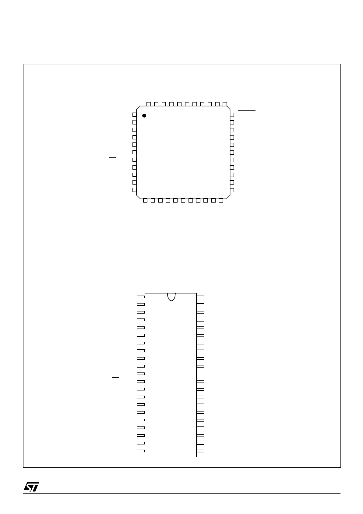
2 PIN DESCRIPTION
Figure 2. 44-pin TQFP and 42-Pin SDIP Package Pinouts
44 43 42 41 40 39 38 37 36 35 34
33
32
31
30
29
28
27
26
25
24
23
12 13 14 15 16 17 18 19 20 21 22
1
2
3
4
5
6
7
8
9
10
11
38
37
36
35
34
33
32
31
30
29
28
27
16
15
1
2
3
4
5
6
7
8
9
10
11
12
13
14
39
40
41
42
PD6
PD5
OSCOUT
OSCIN
IT9 / PC2
IT10 / SCK / PC3
IT11 / SS
/ PC4
IT12 / MISO / PC5
MOSI / PC6
PD1
V
PP
PD2
PD3
PD4
PC7
PD0
V
DDA
USBVCC
PB1 (HS) / RDI
PB0 (HS) / MC O
PA7 / AIN7
PA6 / AIN6
PA5 / AIN5
PA4 / AIN4
PA3 / AIN3 / IT4
PA0 / AIN0 / IT1 / USBOE
RESET
V
SSA
USBDM
USBDP
PA1 / AIN1 / IT2
PA2 / AIN2 / IT3
21
20
17
18
19
IT8 / PWM1 / PB7 (HS)
PC0
PC1
V
DD
V
SS
26
25
24
23
22
PB6 (HS) / PWM0 / IT7 / ICCDATA
PB5 (HS) / ARTIC2 / IT6 / ICCCLK
PB4 (HS) / ARTIC1 / IT5
PB3 (HS) / ARTCLK
PB2 (HS) / TDO
OSCOUT
OSCIN
IT9 / PC2
IT10 / SCK / PC3
IT11 / SS
/ PC4
IT12 / MISO / PC5
MOSI / PC6
PD1
V
PP
PC7
PD0
IT8 / PWM1 / PB7
PC0
PC1
V
DD
V
SS
ARTCLK / PB3 (HS)
IT5 / ARTIC1 / PB4 (HS)
ICCCLK / IT6 / ARTIC2 / PB5 (HS)
ICCDATA /IT7 / PWM0 / PB6 (HS)
N.C.
TDO / PB2 (HS)
PB1 (HS) / RDI
PB0 (HS) / MCO
PA7 / AIN7
PA6 / AIN6
PA5 / AIN5
PA4 / AIN4
PA3 / AIN3 / IT4
PA0 / AIN0 / IT1 / USBOE
RESET
PA1 / AIN1 / IT2
PA2 / AIN2 / IT3
V
DDA
USBVCC
V
SSA
USBDM
USBDP
PD3
PD4
Reserved*
PD6
PD5
PD2
* Pin 39 of the T QFP44 package
must be lef t unconnected.

ST7262
6/132
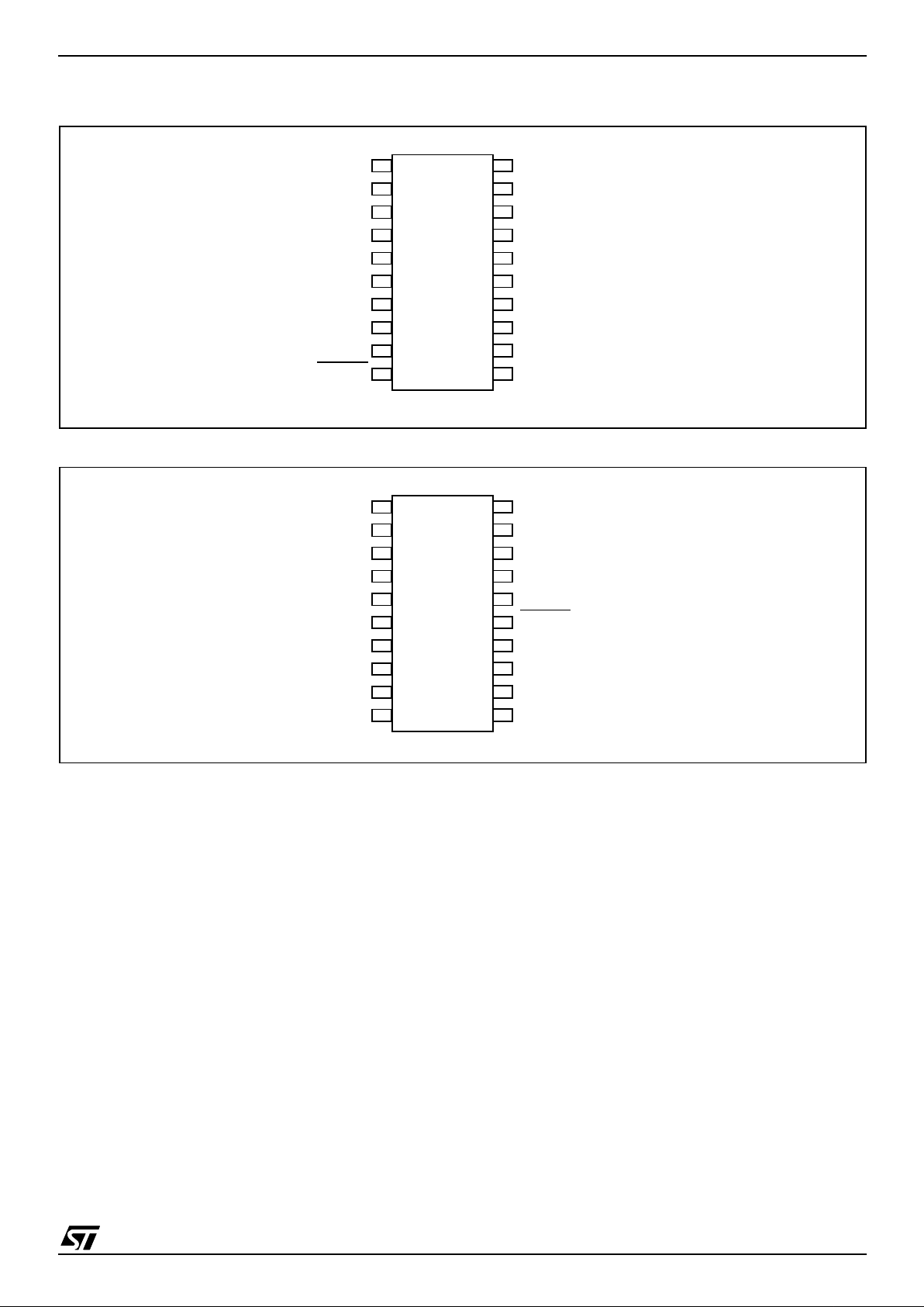
PIN DESCRIPTION (Cont’d)
Figure 3. 34-Pin SO and 32-Pin SDIP Package Pinouts
28
27
26
25
24
23
22
21
20
19
18
29
30
31
32
PC4 / SS / INT11
PC5 / MISO / IT12
PA4 / AIN4
PA3 / AIN3 / IT4
PA2 / AIN2 / IT3
PA1 / AIN1 / IT2
PA0 / AIN0 / IT1 / USBOE
V
SSA
USBDM
USBVCC
V
DDA
V
PP
RESET
PC6 / MOSI
USBDP
PC7
16
15
1
2
3
4
5
6
7
8
9
10
11
12
13
14
IT10 / SCK / PC3
IT9 / PC2
AIN7 / PA7
MCO / PB0 (HS)
RDI / PB1 (HS)
TDO / PB2 (HS)
ARTCLK / PB3 (HS)
IT5 / ARTIC1 / PB4 (HS)
ICCCLK / IT6 /ARTIC2 / PB5 (HS)
IT8 / PWM1 / PB7 (HS)
V
DD
V
SS
OSCOUT
OSCIN
ICCDATA / IT7 / PWM0 / PB6 (HS)
PA5 / AIN5
AIN6 / PA6
33
34
17
28
27
26
25
24
23
22
21
20
19
18
17
16
15
1
2
3
4
5
6
7
8
9
10
11
12
13
14
29
30
31
32
IT10 / SCK / PC3
IT9 / PC2
AIN7 / PA7
MCO / PB0 (HS)
RDI / PB1 (HS)
TDO / PB2 (HS)
ARTCLK / PB3 (HS)
IT5 / ARTIC1 / PB4 (HS)
ICCCLK / IT6 / ARTIC2 / PB5 (HS)
IT8 / PWM1 / PB7 (HS)
V
DD
V
SS
OSCOUT
OSCIN
ICCDATA / IT7 / PWM0 / PB6 (HS)
AIN6 / PA6
PC4 / SS
/ INT11
PC5 / MISO / IT12
PA4 / AIN4
PA3 / AIN3 / IT4
PA2 / AIN2 / IT3
PA1 / AIN1 / IT2
PA0 / AIN0 / IT1 / USBOE
V
SSA
USBDM
USBVCC
V
DDA
V
PP
RESET
PC6 / MOSI
USBDP
PA5 / AIN5
PC1
ST7262
7/132
Figure 4. 20-pin SO20 Package Pinout
Figure 5. 20-pin DIP20 Package Pinout
14
13
12
11
15
16
17
18
OSCIN
OSCOUT
PB7 (HS) / PWM1 / IT8
PB6 (HS) / PWM0 / IT7/ ICCDATA
USBVCC
V
DD
V
PP
USBDP
1
2
3
4
5
6
7
8
9
10
IT3 / AIN2 / PA2
PB0 (HS) / MCO
PB1 (HS)
PB2 (HS)
PB3 (HS) / ARTCLK
PB4 (HS) / ARTIC1 / IT5
RESET
IT2 / AIN1 / PA1
19
20
USBOE/ IT1 / AIN0/ PA0
V
SS
USBDM
PB5 (HS) / ARTIC2 / IT6 / ICCCLK
14
13
12
11
15
16
17
18
OSCIN
OSCOUT
PB7 (HS) / PWM1 / IT8
PB6 (HS) / PWM0 / IT7/ICCDATA
USBVCC
V
DD
V
PP
USBDP
1
2
3
4
5
6
7
8
9
10
IT5 / ARTIC1 / PB4 (HS)
MCO / PB0 (HS)
PB1 (HS)
PB2 (HS)
RESET
IT2 / AIN1/ PA1
19
20
USBOE / IT1 / AIN0 / PA0
V
SS
USBDM
PB5 (HS) / ARTIC2 / IT6 / ICCCLK
IT3 / AIN2 / PA2
ARTCLK / PB3 (HS)
ST7262
8/132
PIN DESCRIPTION (Cont’d)
Legend / Abbreviations:
Type: I = Input, O = Output, S = Supply
Input level: A = Dedicated analog input
Input level: C = CMOS 0.3V
DD
/0.7VDD,
C
T
= CMOS 0.3VDD/0.7VDD with input trigger
Output level: HS = High Sink (on N-buffer only)
Port configuration capabilities:
– Input:float = floatin g, wpu = weak pull-up, int = interrupt (\ =falling edge, / =rising edge
),
ana = analog
– Output: OD = open drain, T = true open drain (N buffer 8mA@0.4 V), PP = push-pull
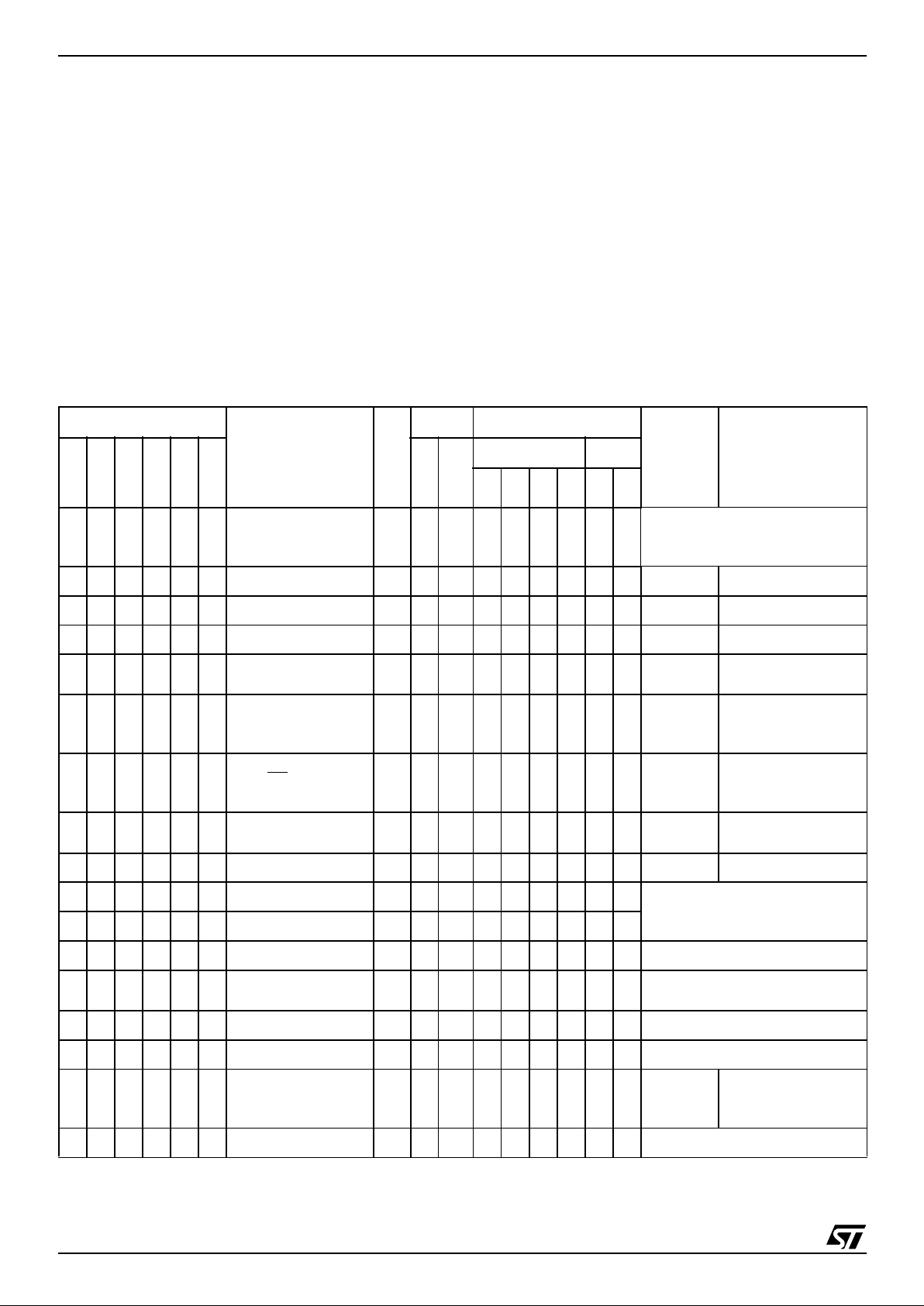
Table 1. Device Pin Description
Pin n°
Pin Name
Type
Level Port / Control
Main
Function
(after
reset)
Alternate Function
TQFP44
DIP42
SO34
DIP32
SO20
DIP20
Input
Output
Input Output
float
wpu
int
ana
OD
PP
1 6 29 28 9 14 V
PP
Sx
FLASH programming voltage
(12V), must be tied low in user
mode.
2 7 - - - - PD1 I/O C
T
xxPort D1
3 8 - - - - PD0 I/O C
T
xxPort D0
4 9 31 - - - PC7 I/O C
T
xxPort C7
5 10 32 30 - - PC6/MOSI I/O C
T
xxPort C6
SPI Master Out /
Slave In
1)
6 11 33 31 - - PC5/MISO/IT12 I/O C
T
xx xPort C5
SPI Master In /
Slave Out 1) /
Interrupt 12 input
7 12 34 32 - - PC4/SS
/IT11 I/O C
T
xx xPort C4
SPI Slave Select
(active low) 1)/
Interrupt 11 input
8 13 1 1 - - PC 3/SCK /IT10 I/O C
T
xx xPort C3
SPI Serial Clock
1)
/
Interrupt 10 input
9 14 2 2 - - PC2/IT9 I/O C
T
xx xPort C2 Interrupt 9 input
10 15 3 3 11 16 OSCIN
These pins are used connect an
external clock source to the onchip main oscillator.
11 16 4 4 12 17 OSCOUT
12175549V
SS
S Digital Ground Voltage
13 18 6 6 8 13 V
DD
S
Digital Main Power Supply Voltage
14 19 7 - - - PC1 I/O C
T
xTPort C1
15 20 - - - - PC0 I/O C
T
xTPort C0
16 21 8 7 13 18
PB7/PWM1/IT8/
RX_SEZ/DATAOUT/DA9
I/O C
T
HS x \ x Port B7
ART PWM output 1/
Interrupt 8 input
17 - - N.C. Not Connected

ST7262
9/132
18 22 9 8 14 19
PB6/PWM0/IT7/
ICCDATA
I/O CTHS x \ x Port B6
ART PWM output 0/
Interrupt 7 input/InCircuit Communication Data
19 23 10 9 15 20
PB5/ARTIC2/IT6/
ICCCLK
I/O C
T
HS x / x Port B5
ART Input Capture 2/
Interrupt 6 input/
In-Circuit Communication Clock
20 24 11 10 16 1 PB4/ARTIC1/IT5 I/O C
T
HS x / x Port B4
ART Input Capture
1/Interrupt 5 input
21 25 12 11 17 2 PB3/ARTCLK I/O C
T
HS x x Port B3 ART Clock input
22 26 13 12 18 3 PB2/TDO I/O C
T
HS x x Port B2
SCI Transmit Data
Output
1)
23 27 14 13 19 4 PB1/RDI I/O CTHS x x Port B1
SCI Receive Data
Input
1)
24 28 15 14 20 5 PB0/MCO I/O CTHS x x Port B0 CPU clock output
25 29 16 15 - - PA7/AIN7 I/O C
T
xxxPort A7 ADC Analog Input 7
26 30 17 16 - - PA6/AIN6 I/O C
T
xxxPort A6 ADC Analog Input 6
27 31 18 17 - - PA5/AIN5 I/O C
T
xxxPort A5 ADC Analog Input 5
28 32 19 18 - - PA4/AIN4 I/O C
T
xxxPort A4 ADC Analog Input 4
29 33 20 19 - - PA3/AIN3/IT4 I/O C
T
x\xxPort A3
ADC Analog Input 3/
Interrupt 4 input
30 34 21 20 1 6 PA2/AIN 2/IT3 I/O C
T
x\xxPort A2
ADC Analog Input 2/
Interrupt 3 input
31 35 22 21 2 7 PA1/AIN 1/IT2 I/O C
T
x\xxPort A1
ADC Analog Input 1/
Interrupt 2 input
32 36 23 22 3 8
PA0/AIN0/IT1 /
USBOE
I/O C
T
x\xxPort A0
ADC Analog Input 0/
Interrupt 1 input/
USB Output Enable
33 37 30 29 10 15 RESET
I/O C
Top priority non maskable interrupt (active low)
34 38 24 23 - - V
SSA
S
Analog Ground Voltage, must
be connected externally to V
SS
.
35 39 25 24 5 10 USBDM I/O USB bidirectional data (data -)
36 40 26 25 6 11 USBDP I/O USB bidirectional data (data +)
37 41 27 26 7 12 USBVCC S USB power supply 3.3V output
38 42 28 27 - - V
DDA
S
Analog Power Supply Voltage,
must be connected externally to
V
DD
.
39 - - - - - Reserved Must be left unconnected.
40 1 - - - - PD6 I/O C
T
xxPort D6
41 2 - - - - PD5 I/O C
T
xxPort D5
42 3 - - - - PD4 I/O C
T
xxPort D4
Pin n°
Pin Name
Type
Level Port / Control
Main
Function
(after
reset)
Alternate Function
TQFP44
DIP42
SO34
DIP32
SO20
DIP20
Input
Output
Input Output
float
wpu
int
ana
OD
PP
ST7262
10/132
Note 1: Peripheral not present on all devices. Refer to “Device Summary” on page 1.
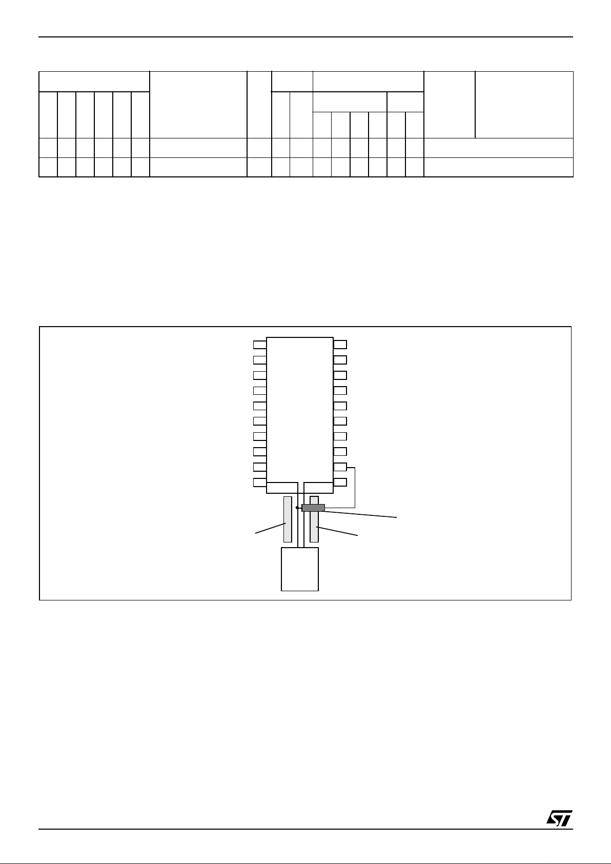
2.1 PCB LAYOUT RECOMMENDATION
In the case of DIP20 de vices the user s hould layout the PCB so that the DIP20 ST7262 device and
the USB connector are centered on the same axis
ensuring that the D- and D+ lines are of equal
length. Refer to Figure 6
Figure 6. Recommended PCB Layout for USB Interface with DIP20 package
43 4 - - - - PD3 I/O C
T
xxPort D3
44 5 - - - - PD2 I/O C
T
xxPort D2
Pin n°
Pin Name
Type
Level Port / Control
Main
Function
(after
reset)
Alternate Function
TQFP44
DIP42
SO34
DIP32
SO20
DIP20
Input
Output
Input Output
float
wpu
int
ana
OD
PP
14
13
12
11
15
16
17
18
USBVCC
USBDP
1
2
3
4
5
6
7
8
9
10
19
20
USBDM
USB Connect o r
Ground
Ground
ST7262
1.5KOhm pull-up resistor
ST7262
11/132
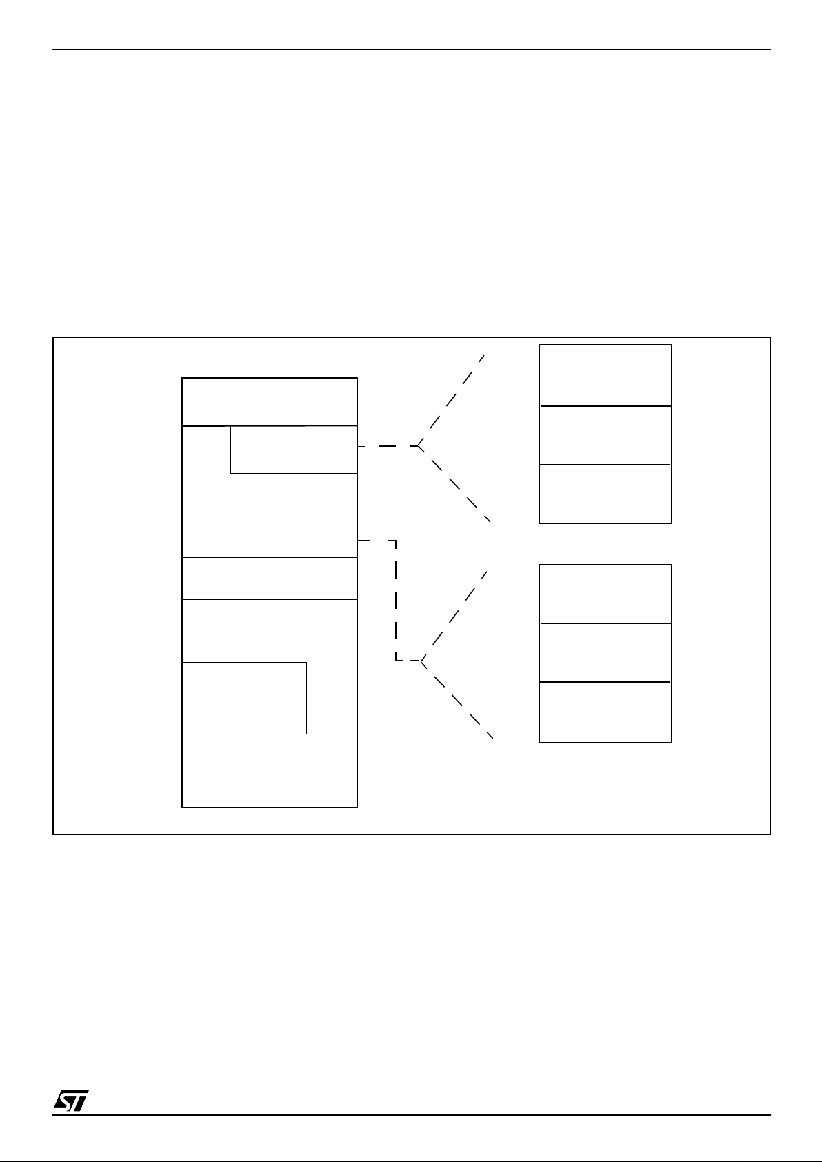
3 REGISTER & MEMORY MAP
As shown in the Figure 7, the MCU i s capable of
addressing 64K bytes of memories and I/O registers.
The available memory locations consist of 64
bytes of register locations, 768 bytes of RA M and
up to 16 Kbytes of user program memory. The
RAM space includes u p to 128 by t es fo r the stack
from 0100h to 017Fh.
The highest address b ytes contain the user res et
and interrupt vectors.
IMPORTANT: Memory locations marked as “Reserved” must ne ver be accessed. A ccessi ng a reseved area can have u npredict able effects on the
device.
Figure 7. Me m ory M a p
0000h
Program Memory
Interrupt & Reset Vectors
HW Registers
BFFFh
0040h
003Fh
(see Table 2)
C000h
FFDFh
FFE0h
FFFFh
(see Table 6)
0340h
Reserved
033Fh
Short Addressing
RAM (zero page)
or Stack
017Fh
0040h
00FFh
768 Bytes RAM
E000h
8 KBytes
(128 Bytes)
16 KBytes
384 Bytes RAM
64 Bytes
01BFh
16-bit Addressing
RAM
Short Addressing
RAM (zero page)
017Fh
0040h
00FFh
448 Bytes
033Fh
16-bit Addressing
RAM
16-bit Addressing
RAM
or Stack
(128 Bytes)
16-bit Addressing
RAM
192 Bytes
192 Bytes
ST7262
12/132
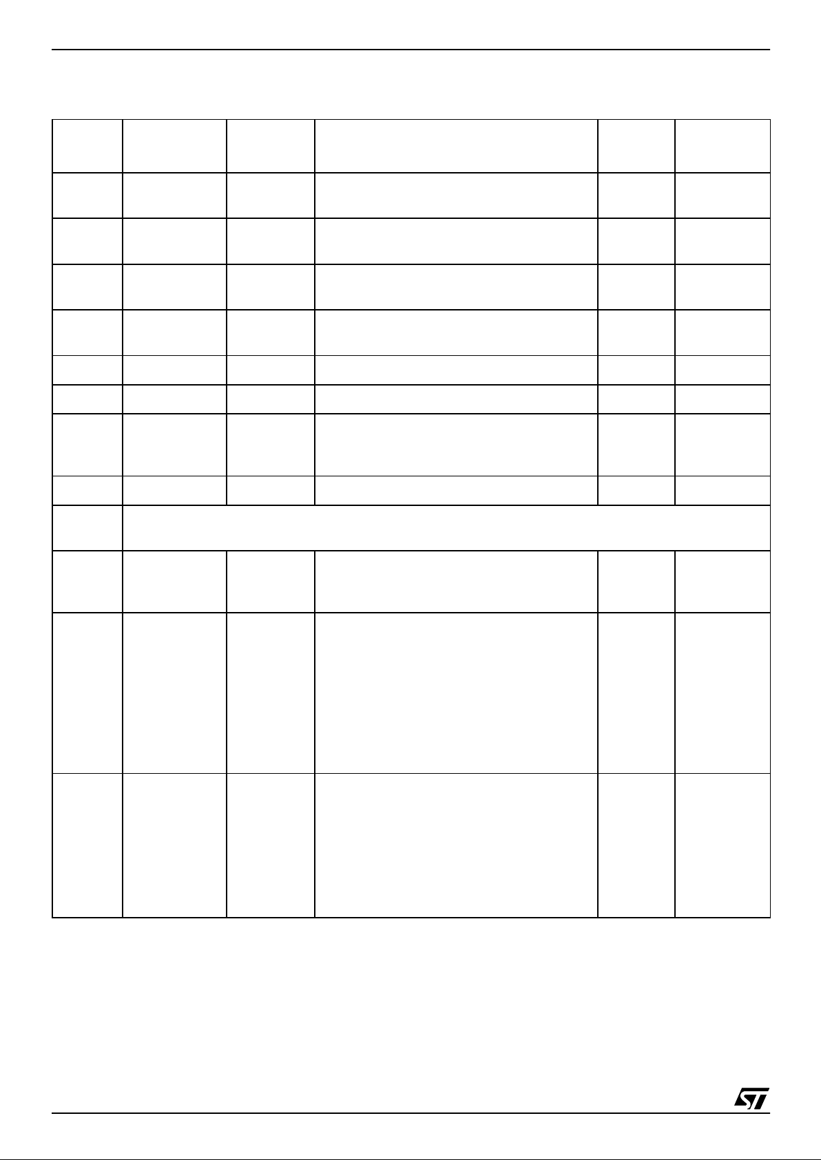
Table 2. Hardware Register M ap
Address Block
Register
Label
Register Name
Reset
Status
Remarks
0000h
0001h
Port A
PADR
PADDR
Port A Data Register
Port A Data Direction Register
00h
1)
00h
R/W
2)
R/W
2)
0002h
0003h
Port B
PBDR
PBDDR
Port B Data Register
Port B Data Direction Register
00h
1)
00h
R/W
2)
R/W
2)
0004h
0005h
Port C
PCDR
PCDDR
Port C Data Register
Port C Data Direction Register
00h
1)
00h
R/W
2)
R/W
2)
0006h
0007h
Port D
PDDR
PDDDR
Port D Data Register
Port D Data Direction Register
00h
1)
00h
R/W
2)
R/W
2)
0008h ITRFRE1 Interrupt Register 1 00h R/W
0009h MISC Miscellaneous Register 00h R/W
000Ah
000Bh
000Ch
ADC
ADCDRMSB
ADCDRLSB
ADCCSR
ADC Data Register (bit 9:2)
ADC Data Register (bit 1:0)
ADC Control Status Register
00h
00h
00h
Read Only
Read Only
R/W
000Dh WDG WDGCR Watchdog Control Register 7Fh R/W
000Eh
0010h
Reserved Area (3 Bytes)
0011h
0012h
0013h
SPI
SPIDR
SPICR
SPICSR
SPI Data I/O Register
SPI Control Register
SPI Control Status Register
xxh
0xh
00h
R/W
R/W
Read Only
0014h
0015h
0016h
0017h
0018h
0019h
001Ah
001Bh
001Ch
PWM ART
PWMDCR1
PWMDCR0
PWMCR
ARTCSR
ARTCAR
ARTARR
ARTICCSR
ARTICR1
ARTICR2
PWM AR Timer Duty Cycle Register 1
PWM AR Timer Duty Cycle Register 0
PWM AR Timer Control Register
Auto-Reload Timer Control/Status Register
Auto-Reload Timer Counter Access Register
Auto-Reload Timer Auto-Reload Register
ART Input Capture Control/Status Register
ART Input Capture Register 1
ART Input Capture Register 2
00h
00h
00h
00h
00h
00h
00h
00h
00h
R/W
R/W
R/W
R/W
R/W
R/W
R/W
Read Only
Read Only
001Dh
001Eh
001Fh
0020h
0021h
0022h
0023h
0024h
SCI
SCIERPR
SCIETPR
SCISR
SCIDR
SCIBRR
SCICR1
SCICR2
SCI Extended Receive Prescaler register
SCI Extended Transmit Prescaler Register
Reserved Area
SCI Status register
SCI Data register
SCI Baud Rate Register
SCI Control Register 1
SCI Control Register 2
00h
00h
--
C0h
xxh
00h
x000 0000b
00h
R/W
R/W
Read Only
R/W
R/W
R/W
R/W

ST7262
13/132
Legend: x=undefined, R/W=read/write
Notes:
1. The contents of the I/O port DR regist ers are readable only in out put conf iguration. I n i nput conf iguration, the values of the I/O pins are returned instead of the DR register contents.
2. The bits associated with unavailable pins must always be kept at their reset value.
0025h
0026h
0027h
0028h
0029h
002Ah
002Bh
002Ch
002Dh
002Eh
002Fh
0030h
0031h
USB
USBPIDR
USBDMAR
USBIDR
USBISTR
USBIMR
USBCTLR
USBDADDR
USBEP0RA
USBEP0RB
USBEP1RA
USBEP1RB
USBEP2RA
USBEP2RB
USB PID Register
USB DMA Address register
USB Interrupt/DMA Register
USB Interrupt Status Register
USB Interrupt Mask Register
USB Control Register
USB Device Address Register
USB Endpoint 0 Register A
USB Endpoint 0 Register B
USB Endpoint 1 Register A
USB Endpoint 1 Register B
USB Endpoint 2 Register A
USB Endpoint 2 Register B
x0h
xxh
x0h
00h
00h
06h
00h
0000 xxxxb
80h
0000 xxxxb
0000 xxxxb
0000 xxxxb
0000 xxxxb
Read Only
R/W
R/W
R/W
R/W
R/W
R/W
R/W
R/W
R/W
R/W
R/W
R/W
0032h
to
0035h
Reserved Area (4 Bytes)
0032h
0033h
0034h
0035h
ITC
ITSPR0
ITSPR1
ITSPR2
ITSPR3
Interrupt Software Priority Register 0
Interrupt Software Priority Register1
Interrupt Software Priority Register 2
Interrupt Software Priority Register 3
FFh
FFh
FFh
FFh
R/W
R/W
R/W
R/W
0036h
0037h
TBU
TBUCV
TBUCSR
TBU Counter Value Register
TBU Control/Status Register
00h
00h
R/W
R/W
0038h FLASH FCSR Flash Control/Status Register 00h R/W
0039h ITRFRE2 Interrupt Register 2 00h R/W
003Ah
to
003Fh
Reserved Area (6 Bytes)
Address Block
Register
Label
Register Name
Reset
Status
Remarks

ST7262
14/132
4 FLASH PROGRAM MEMORY
4.1 Introduction
The ST7 dual voltage High Density Flash
(HDFlash) is a non-volatile memory that can be
electrically erased as a single block or by individual sectors and programmed on a Byte-by-Byte basis using an external V
PP
supply.
The HDFlash devices can be programmed and
erased off-board (plugge d in a programm ing tool)
or on-board using ICP (In-Circuit Programming) or
IAP (In-Application Programming).
The array matrix organ isation allows each sector
to be erased and reprogramm ed without affecting
other sectors.
4.2 Main Features
■ Three Flash programming modes :
– Insertion in a programming tool. In this m ode,
all sectors including option bytes can be programmed or erased.
– ICP (In-Circuit Programming). In this mode, all
sectors including option bytes can be programmed or erased without removing the device from the application board.
– IAP (In-Application Programming) In this
mode, all sectors except Sector 0, can be programmed or erased without removing the device from the application board a nd wh ile the
application is running.
■ ICT (In-Circuit Testing) for downloading and
executing user application test patterns in RAM
■ Read-out protection against piracy
■ Register Access Security System (RASS) to
prevent accidental programming or erasing
4. 3 S truct u re
The Flash memory is organised in sectors and can
be used for both code and data storage.
Depending on the overall Flash memory size in the
microcontroller device, there are up to three user
sectors (see Tab le 3). Each of these sectors can
be erased independently to avoid unnecessary
erasing of the whole Flas h memory when only a
partial erasing is required.
The first two sectors have a fixed siz e of 4 Kby tes
(see Figure 8). They are mapped in the upper part
of the ST7 addressing space so t he reset and interrupt vectors are located in Sector 0 (F000hFFFFh).
Table 3. Sectors available in Flash devices
4.3.1 Read-out Protection
Read-out protection, when s elected, makes it impossible to extract the memory content from the
microcontroller, thus preventing piracy. Even ST
cannot access the user code.
In flash devices, this protection is removed by reprogramming the option. In this case, the entire
program memory is first automatically erased and
the device can be reprogrammed.
Read-out protection selection depend s on the device type:
– In Flash devices it is enabled and removed
through the FMP_R bit in the option byte.
– In ROM devices it is enabled by mask option
specified in the Option List.
Figure 8. Me m ory M a p and Sector A dd r ess
Flash Size (bytes) Available Sectors
4K Sector 0
8K Sectors 0,1
> 8K Sectors 0,1, 2
4 Kbytes
4 Kbytes
2Kbytes
SECTOR 1
SECTOR 0
16 Kbytes
SECTOR 2
8K 16K 32K 60K
FLASH
FFFFh
EFFFh
DFFFh
3FFFh
7FFFh
1000h
24 Kbytes
MEMORY SIZE
8Kbytes 40 Kbytes
52 Kbytes
9FFFh
BFFFh
D7FFh
4K 10K 24K 48K

ST7262
15/132
FLASH PROGRAM MEMORY (Cont’d)
4.4 ICC Interface
ICC needs a m inimum of 4 and up to 6 pins to b e
connected to the programming tool (see Figure 9).
These pins are:
– RESET
: device reset
–V
SS
: device power supply ground
– ICCCLK: ICC output serial clock pin
– ICCDATA: ICC input/output serial data pin
– ICCSEL/V
PP
: programming voltage
– OSC1(or OSCIN): main clock in put for exter-
nal source (optional)
–V
DD
: application board power su pply (option-
al, see Figure 9, Note 3)
Figure 9. Typical ICC Interface
Notes:
1. If the ICCCLK or ICCDATA pins are only u sed
as outputs in t he ap plication, n o s ign al iso lation is
necessary. As soon as the Programming Tool is
plugged to the board, even if an ICC session is not
in progress, the ICCCLK and ICCDATA pins are
not available for the application. If they are used as
inputs by the application, isolation such as a serial
resistor has to implemented in case another device forces the signal. Refer to the Programming
Tool documentation for recommended resistor values.
2. During the ICC session, the programming tool
must control the RESET
pin. This can lead to conflicts between the programming tool and the application reset circuit if it drives more than 5mA at
high level (push pull output or pull-up resistor<1K).
A schottky diode can be us ed to iso late the application RESET circuit in this case. When using a
classical RC network with R>1K or a reset man-
agement IC with open drain ou tput and pu ll-up resistor>1K, no additional com ponents are needed.
In all cases the user must ensure that no external
reset is generated by the application during the
ICC session.
3. The use of Pin 7 of the ICC con nector de pends
on the Programming Tool architecture. This pin
must be connected when using most ST Programming Tools (it is used to monitor the application
power supply). Please refer to the Programming
Tool manual.
4. Pin 9 has to be co nnected to the OS C1 or OSCIN pin of the ST7 when the clock is not available
in the application or if the sel ected clock opt ion is
not programmed in t he option byte. ST7 devices
with multi-oscillator capability need to have OSC2
grounded in this case.
ICC CONNECTOR
ICCDATA
ICCCLK
RESET
V
DD
HE10 CONNECTOR TYPE
APPLICATION
POWER SUPPLY
1
246810
975 3
PROGRAMMING TOOL
ICC CONNECTOR
APPLICATION BOARD
ICC Cab le
OPTIONAL
(See No te 3)
10k
Ω
V
SS
ICCSEL/VPP
ST7
C
L2
C
L1
OSC1
OSC2
OPTIONAL
See Note 1
See Note 2
APPLICATION
RESET SOURCE
APPLICATI ON
I/O
(See No te 4)

ST7262
16/132
FLASH PROGRAM MEMORY (Cont’d)
4.5 ICP (In-Circuit Programming)
To perform ICP the microcontroller must be
switched to ICC (In-Circuit Communication) mode
by an external controller or programming tool.
Depending on the ICP code dow nloaded in RAM,
Flash memory programming can be fully customized (number of bytes to prog ram, program locations, or selection serial communication interface
for downloading).
When using an STMicroelectronics or third-party
programming tool that supp orts ICP and the specific microcontroller device, the user needs only to
implement the ICP hardware interface on the application board (see Figure 9). For more details on
the pin locations, refer to the device pinout description.
4.6 IA P ( I n-Application Programming)
This mode uses a BootLoader program previously
stored in Sector 0 by the us er (in ICP mode or by
plugging the device in a programming tool).
This mode is fully controlled by user software. This
allows it to be adapted to the user application, (user-defined strategy for entering programming
mode, choice of comm unications protocol used to
fetch the data to be stored, etc.). For example, it is
possible to download code from the SPI, SCI, USB
or CAN interface and program it in the Fl ash. IAP
mode can be used to program any of the Flash
sectors except Sector 0, which i s write/erase protected to allow recovery in case errors occur during the programming operation.
4.7 Related Documentation
For details on Flash program ming and ICC protocol, refer to the ST7 Flash Programming Reference Manual and to the ST7 ICC Protocol Re ference Manual
.
4.8 Register Description
FLASH CONTROL/STATUS REGISTER (FCSR)
Read/Write
Reset Value: 0000 0000 (00h)
This register is reserved for use by Programming
Tool software. It controls the Flash programming
and erasing operations.
70
00000000
ST7262
17/132
5 CENTRAL PRO CESSING UNIT
5.1 INTRODUCTION
This CPU has a full 8-bit architecture and contains
six internal registers allowing efficient 8-bit data
manipulation.
5.2 MAIN FEATURES
■ Enable executing 63 basic instructions
■ Fast 8-bit by 8-bit multiply
■ 17 main addressing modes (with indirect
addressing mode)
■ Two 8-bit index registers
■ 16-bit stack pointer
■ Low power HALT and WAIT modes
■ Priority maskable hardware interrupts
■ Non-maskable software/hardware interrupts
5.3 CPU REGISTERS
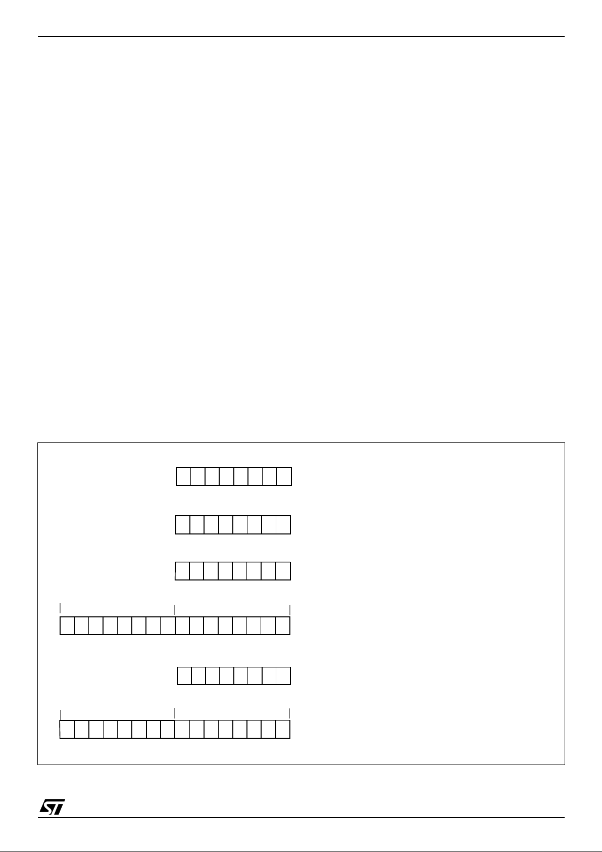
The 6 CPU registers shown in Figure 10 are not
present in the memory mapping and are accessed
by spec ifi c ins t ru c tio n s .
Accumulator (A)
The Accumulator is an 8-bit general purpose register used to hold operands and the res ults of the
arithmetic and logic calculations and to manipulate
data.
Index Registers (X and Y)
These 8-bit registers are used to create effective
addresses or as tempo rary storage areas f or data
manipulation. (The Cross -Assembler generates a
precede instruction (PRE) to indicate that the following instruction refers to the Y register.)
The Y register is not affected by the interrupt automatic procedures.
Program Counter (PC)
The program counter is a 16-bit register containing
the address of the next instruction to be executed
by the CPU. It is made of two 8-bit registers PCL
(Program Counter Low which is the LSB) and PCH
(Program Counter High which is the MSB).
Figure 10. CPU Registers
ACCUMULATOR
X INDEX REGISTER
Y INDEX REGISTER
STACK POINTER
CONDITION CODE REGISTER
PROGRAM COUNTER
70
1C1I1HI0NZ
RESET VALUE = RESET VECTOR @ FFFEh-FFFFh
70
70
70
0
7
15 8
PCH
PCL
15
8
70
RESET VALUE = STACK HIGHER ADDRESS
RESET VALUE =
1X11X1XX
RESET VALUE = XXh
RESET VALUE = XXh
RESET VALUE = XXh
X = Undefined Value

ST7262
18/132
CENTRAL PROC ESSING UNIT (Cont’d)
Condition Code Reg ister (CC)
Read/Write
Reset Value: 111x1xxx
The 8-bit Condition Code regist er contains the i nterrupt masks and four flags representative of the
result of the instruction just executed. This register
can also be handled by the PUSH and POP instructions.
These bits can be individually tested and/or controlled by specific instructions.
Arithmetic Management Bits
Bit 4 = H
Half carry
.
This bit is set by hardware when a carry occurs between bits 3 and 4 of t he ALU during an ADD or
ADC instructions. It is reset by hardware during
the same instructio n s.
0: No half carry has occurred.
1: A half carry has occurred.
This bit is tested using the JRH or JRNH in struction. The H bit is useful in BCD arithmetic subroutine s .
Bit 2 = N
Negative
.
This bit is set and cleared by hardware. It is representative of the result sign of the last arithmetic,
logical or data manipulation. I t’s a copy of the result 7
th
bit.
0: The result of the last operation is positive or null.
1: The result of the last operation is negative
(i.e. the most significant bit is a logic 1).
This bit is accesse d by the JRMI and JRPL instructions.
Bit 1 = Z
Zero
.
This bit is set and cleared by hardware. This bit indicates that the result of the last arithme tic, logical
or data manipulation is zero.
0: The result of the last operation is dif ferent from
zero.
1: The result of the last operation is zero.
This bit is accessed by the JREQ and JRNE test
instructions.
Bit 0 = C
Carry/borrow.
This bit is set and cleared b y hardware and software. It indicates an overflow or an un derflow has
occurred during the last arithmetic operation.
0: No overflow or underflow has occurred.
1: An overflow or underflow has occurred.
This bit is driven by th e SCF and RCF instructions
and tested by the JRC and JRNC instructions. It i s
also affected by the “bit test and branch”, shift and
rotate instructions.
Interrupt Managem e nt B i ts
Bit 5,3 = I1, I0
Interrupt
The combination of the I1 and I0 bits gives the current interrupt software priority.
These two bits are set/cleared by hardware when
entering in interrupt. The loaded value is given by
the corresponding bits in the interrupt software priority registers (IxSPR). They can be also set/
cleared by software with the RIM, SIM, IRET,
HALT, WFI and PUSH/POP instructions.
See the interrupt management chapter for more
details.
70
11I1HI0NZ
C
Interrupt Software Priorit y I1 I0
Level 0 (main) 1 0
Level 1 0 1
Level 2 0 0
Level 3 (= interrupt disable) 1 1

ST7262
19/132
CPU REGISTERS (Cont’d)
STACK POINTER (SP)
Read/Write
Reset Value: 017Fh
The Stack Pointer is a 16-bit register which is always pointing to the next free location in the stack.
It is then decremented after data has been pushed
onto the stack and incremented before data is
popped from the stack (see Figure 11).
Since the stack is 128 bytes deep, the 9 most significant bits are forced by hard ware. Following a n
MCU Reset, or after a Reset Stack Pointer instruction (RSP), the Stack Pointer contains its reset value (the SP6 to SP0 bits are set) which is the stack
higher address.
The least significant byte of the Stack Pointer
(called S) can be directly accessed by a LD instruction.
Note: When the lower limit is exceeded, the Stack
Pointer wraps around to the stack upper limit, without indicating the stack overflow. The previously
stored information is then o verwritten and therefore lost. The stack also wraps in case of an underflow.
The stack is used to sav e the return address during a subroutine call and the CPU context during
an interrupt. The user may also directly manipulate
the stack by means of the PUSH and POP instructions. In the case of an interrupt, the PCL is stored
at the first location po inted t o by t he SP. Th en t he
other registers are stored in the next locations as
shown in Figure 11.
– When an interrupt is received, the SP is decre-
mented and the context is pushed on the stack.
– On return from interrupt, the SP is incremented
and the context is popped from the stack.
A subroutine call occupies two locations and an interrupt five locat ion s i n the stack ar ea.
Figure 11. Stack Manipulation Examp le
15 8
00000001
70
1 SP6 SP5 SP4 S P3 SP2 S P1 SP0
PCH
PCL
SP
PCH
PCL
SP
PCL
PCH
X
A
CC
PCH
PCL
SP
PCL
PCH
X
A
CC
PCH
PCL
SP
PCL
PCH
X
A
CC
PCH
PCL
SP
SP
Y
CALL
Subroutine
Interrupt
Event
PUSH Y POP Y IRET
RET
or RSP
@ 017Fh
@ 0100h
Stack Higher Address = 017Fh
Stack Lower Address =
0100h
ST7262
20/132
6 CLOCKS AND RESET
6.1 CLOCK SYSTEM
6.1.1 General Description
The MCU accepts either a Crystal or Ceramic resonator, or an external clock signal to drive the internal oscillator. The internal clock (f
CPU
) is de-
rived from the external oscillator frequency (f
OSC
),
by dividing by 3 and multiplying by 2. By setting the
OSC12/6 bit in the option byte, a 12 MHz ex ternal
clock can be used giving an internal frequency of 8
MHz while maintaining a 6 MHz clock for USB (refer to Figure 14).
The internal clock signal (f
CPU
) consists of a
square wave with a duty cycle of 50%.
It is further divided by 1, 2, 4 or 8 depending on the
Slow Mode Selection bits in the Miscellaneous
register ( SMS[1:0 ])
The internal oscillat or is designed to operate with
an AT-cut parallel resonant quartz or ceramic resonator in the frequency range specified for f
osc
.
The circuit shown in Figure 13 is recommended
when using a crystal, and Table 4 lists the recommended capacitors. The crystal and associated
components shoul d be m ounted as close as possible to the input pins in o rder to minimize output
distortion and start-up stabilization time.
Table 4. Recommended Values for 12 MHz
Crystal Resonator
Note: R
SMAX
is the equivalent serial resistor of the
crystal (see crystal specification).
6.1.2 External Clock input
An external clock may be applied to the OSCIN input with the OSCOUT pin not connected, as
shown on Figure 12. The t
OXOV
specifications
does not apply when using an external clock input.
The equivalent specification of the external clock
source should be used instead of t
OXOV
(see Elec-
tr ical Characte ristics).
6.1.3 Clock Output Pin (MCO)
The internal clock (f
CPU
) can be output on Port B0
by setting the MCO bit in the Misce llaneous register.
Figure 12. External Clock Source Connections
Figure 13. Crystal/Ceramic Resonator
Figure 14. Clock block diagram
R
SMAX
20
Ω
25
Ω
70
Ω
C
OSCIN
56pF 47pF 22pF
C
OSCOUT
56pF 47pF 22pF
R
P
1-10 M
Ω
1-10 M
Ω
1-10 M
Ω
OSCIN OSCOUT
EXTERNAL
CLOCK
NC
OSCIN
OSCOUT
C
OSCIN
C
OSCOUT
to CPU and
f
CPU
8/4/2/1 MHz
6 MHz (USB)
12 or
peripherals
%2
0
1
OSC12/6
6 MHz
Crystal
x2
Slow
Mode
%
SMS[1:0]
1/2/4/8
%3
(or 4/2/1/0.5 MHz)
MCO pin

ST7262
21/132
6.2 RESET
The Reset procedure is used to provide an orderly
software start-up or to exit low power modes.
Three reset modes are provided: a low voltage reset, a watchdog reset and an ext ernal reset at the
RESET
pin.
A reset causes the reset vector to be fetched from
addresses FFFEh and FFFFh in order to be loaded
into the PC and with program execution starting
from this point.
An internal circuitry provides a 5 14 CPU clock cycle delay from the time that the oscillator becomes
active.
6.2.1 Low Voltage Reset
Low voltage reset circuitry generates a reset when
V
DD
is:
■ below V
IT+
when VDD is rising,
■ below V
IT-
when VDD is falling.
During low voltage reset, the RESET
pin is held low,
thus permitting the MCU to reset other devices.
The Low Voltage Detector can be disabled by setting the LVD bit of the Option byte.
6.2.2 Watchdog Reset
When a watchdo g reset occ urs, t he RESET
pin is
pulled low permitting the MCU to reset other devices as when low voltage reset (Figure 15 ).
6.2.3 External Reset
The external reset is an active low input signal applied to the RESET
pin of the MCU.
As shown in Figure 18, the RESET
signal must
stay low for a minimum of one and a half CPU
clock cycles.
An internal Schmitt trigger at the RESET
pin is pro-
vided to improve noise immunity.
Figure 15. Low Voltage Reset functional Diagram
Figure 16. Low Voltage Reset Signal Output
Note: Typical hysteresis (V
IT+-VIT-
) of 250 mV is
expected
Figure 17. Temporization Timing Diagram after an internal Reset
LOW VOLTAGE
V
DD
FROM
WATCHDOG
RESET
RESET
INTERNAL
RESET
RESET
RESET
V
DD
V
IT+
V
IT-
V
DD
Addresses
$FFFE
Temporization
V
IT+
(514 CPU clock cycles)
ST7262
22/132
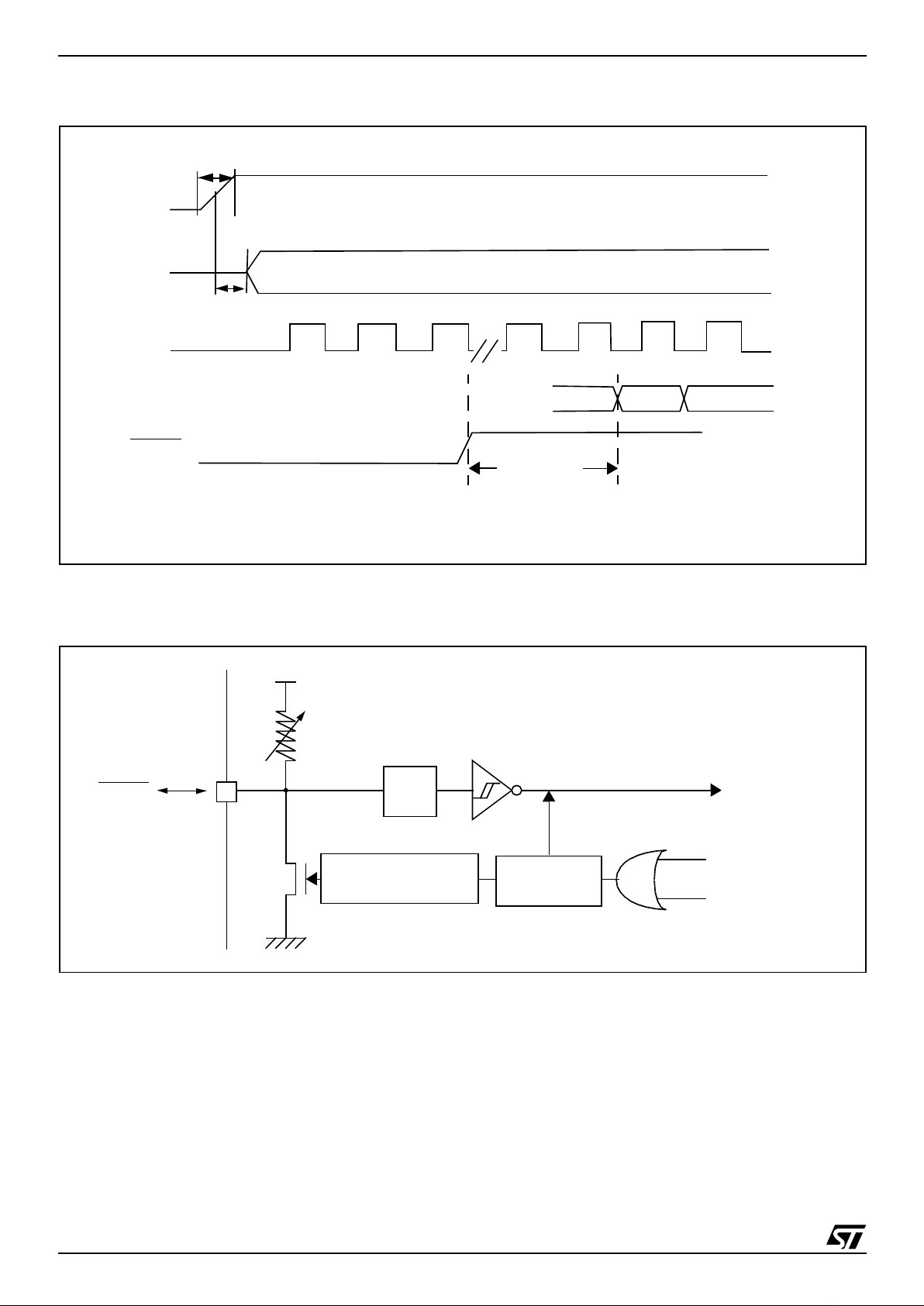
Figure 18. Reset Timing Diagra m
Note: Refer to Electrical Characteristics for values of t
DDR
, t
OXOV
, V
IT+
and V
IT-.
Figure 19. Reset Block Diagram
Note: The output of the external reset circuit must have an open-drain output to drive the ST7 reset pad.
Otherwise the device can be damaged when the ST7 generates an internal reset (LVD or watchdog).
V
DD
OSCIN
f
CPU
FFFF
FFFE
PC
RESET
t
DDR
t
OXOV
514 CPU
CLOCK
CYCLES
DELAY
RESET
R
ON
V
DD
WATCHDOG RESET
LVD RESET
INTERNAL
RESET
PULSE
GENERATOR
200ns
Filter
t
w(RSTL)out
+ 128 f
OSC
delay

ST7262
23/132
7 INTERRUP T S
7.1 INTRODUCTION
The CPU enhanced interrupt management provides the following features:
■ Hardware interrupts
■ Software interrupt (TRAP)
■ Nested or concurrent interrupt management
with flexible interrupt priority and level
management:
– Up to 4 software programmable nesting levels
– Up to 16 interrupt vectors fixed by hardware
– 3 non maskable events: RESET, TRAP, TLI
This interrupt management is based on:
– Bit 5 and bit 3 of the CPU CC register (I1:0),
– Interrupt software priority registers (ISPRx),
– F ixed interrupt vecto r addresses locat ed at the
high addresses of the memory map (FFE0h to
FFFFh) sorted by hardware priority order.
This enhanced interrupt cont roller guarantees full
upward compatibility with the standard (not nested) CPU interrupt controller.
7.2 MASKING AND PROC ESSING FLOW
The interrupt masking is managed by the I1 and I0
bits of the CC register and the ISPRx registers
which give the interrupt software priority level of
each interrupt vector (see Table 5 ). The processing flow is shown in Fi gure 20.
When an interrupt request has to be serviced:
– Normal processing is suspended at the end of
the current instruction execution.
– The PC, X, A and CC registers are saved onto
the stack.
– I1 and I0 bits of CC register are set according to
the corresponding values in the ISPRx registers
of the serviced interrupt vector.
– The PC is then loaded with the interrupt vector of
the interrupt to service and the first instruction of
the interrupt service routine is fetched (refer to
“Interrupt Mapping” table for vector addresses).
The interrupt service routine should end with the
IRET instruction which c auses the contents of t he
saved registers to be recovered from the stack.
Note: As a cons equence of the IRET instruction,
the I1 and I0 bits will be restored from the stack
and the program in the previous level will resume.
Table 5. Interrupt Software Priority Levels
Figure 20. Int errupt Processing Flowchart
Interrupt software priority Le vel I1 I0
Level 0 (main) Low
High
10
Level 1 0 1
Level 2 0 0
Level 3 (= interrupt disable) 1 1
“IRET”
RESTORE PC, X, A, CC
STACK PC, X, A, CC
LOAD I1:0 FRO M INTER RUPT SW REG.
FETCH NEX T
RESET
TLI
PENDING
INSTRUCTION
I1:0
FROM STACK
LOAD PC FROM INTERRUPT VECTOR
Y
N
Y
N
Y
N
Interrupt has the same or a
lower software priority
THE INTERRUPT
STAYS PENDING
than c u rrent one
Interrupt has a higher
softwarepriority
than current one
EXECUTE
INSTRUCTION
INTERRUPT
ST7262
24/132
INTERRUPTS (Cont’d)
Servicing Pending In te rrupts
As several interrupts can b e pen ding at the s ame
time, the interrupt to be taken into account is determined by the following two-step process:
– the highest software priority interrupt is serviced,
– i f several interrupts have the same software pri-
ority then the interrupt with the highest hardware
priority is serviced first.
Figure 21 describes this decision process.
Figure 21. Priority Decision Process
When an interrupt request is not serviced immediately, it is latched and then processed when its
software priority combined with the hardware priority becomes the highest one.
Note 1: The hardware priority is exclusive while
the software one i s not. This allows the prev ious
process to succeed with only one interrupt.
Note 2: RESET, TRAP and TLI can be considered
as having the highest softwa re priority in the d ecision process.
Different Interrupt Vector Sources
Two interrupt source types are managed by the
CPU interrupt controller: the non-maskable type
(RESET, TLI, TRAP) and the maskable type (external or from internal peripherals).
Non-Maskable Sources
These sources are processed regardless of the
state of the I1 and I0 bits of the CC register (see
Figure 20). After stacking the PC, X, A and CC
registers (except for RESET), the corresponding
vector is loaded in the PC register and t he I1 and
I0 bits of the CC are set to disable interrupts (level
3). These sources allow the processor to exit
HALT mode.
■ TLI (Top Level Hardware Interrupt)
This hardware interrupt occurs when a specific
edge is detected on the dedicated TLI pin.
Caution: A TRAP instruction must not be used in a
TLI service routine.
■ TRAP (Non Maskable Software Interrupt)
This software interrupt is serviced when the TRAP
instruction is executed. It will be serviced according to the flowchart in Figure 20 as a TLI.
Caution: TRAP can be interrupted by a TLI.
■ RESET
The RESET source has the highe st priority in the
CPU. This means that the first current routine has
the highest software priority (level 3) and the highest hardware priority.
See the RESET chapter for more details.
Maskable Sources
Maskable interrup t vector sourc es can be servi ced
if the corresponding in terrupt is enabled and if its
own interrupt software priority (in ISPRx registers)
is higher than the one currently being serviced (I1
and I0 in CC register). If any of these two co nditions is false, the interrupt is la tched and thus remains pending.
■ External Interrupts
External interrupts allow the processor to exit from
HALT low power mode.
External interrupt sensitivity is software selectable
through the ITRFRE2 register.
External interrupt triggered on edge will be latched
and the interrupt request automatically cleared
upon entering the interrupt service routine.
If several input pins of a group connected to the
same interrupt line are selected simultaneously,
these w ill be log i cally NANDed.
■ Peripheral Interrupts
Usually the peripheral interrupts cause the Device
to exit from HALT mode except those mentioned in
the “Interrupt Mapping” table.
A peripheral interrupt occurs when a specific flag
is set in the peripheral status registers and if the
corresponding enable bit is set in the peripheral
control register.
The general sequence for clearing an interrupt is
based on an access to the status register followed
by a read or write to an associated register.
Note: The clearing sequence resets the internal
latch. A pending interrupt (i.e. waiting for being
serviced) will therefore be lost if the clear sequence is executed.
PENDING
SOFTWARE
Different
INTERRUPTS
Same
HIGHEST HARDWARE
PRIORITY SERVICED
PRIORITY
HIGHEST SOFTWARE
PRIORITY SERVICED
ST7262
25/132
INTERRUPTS (Cont’d)
7.3 INTERRUPTS AND LOW POWER MODES
All interrupts allow the processor to exit the WAIT
low power mode. On the contrary, only external
and other specified interrupt s allow the processor
to exit from the HALT modes (see column “Exit
from HALT” in “Interrupt Mapping” table). When
several pending interrupts are present whi le exiting HALT mode, the first one serviced can only be
an interrupt with e xit from HALT mode c apability
and it is selected through the same decision proc ess shown in Figure 21.
Note: If an interrupt, that is not able to Exit from
HALT mode, is pending with the highest priority
when exiting HALT mode, this interrupt is serviced
after the first one serviced.
7.4 CONCURRENT & NESTED MANAGEMENT
The following Figure 22 and Figure 23 show two
different interrupt management modes. The first is
called concurrent mode and do es not allow an interrupt to be interrupted, unlike the nested mode in
Figure 23. The interrupt hardware priority is given
in this order from the l owes t to the hi ghest: M A IN,
IT4, IT3 , IT2, IT1, IT0, TLI. The software priority is
given for each interrupt.
Warning: A stack overflow may occur without notifying the software of the failure.
Figure 22. Concurrent Interru pt Manage m ent
Figure 23. Nested Interrupt Management
MAIN
IT4
IT2
IT1
TLI
IT1
MAIN
IT0
I1
HARDWARE PRIORITY
SOFTWARE
3
3
3
3
3
3/0
3
11
11
11
11
11
11 / 10
11
RIM
IT2
IT1
IT4
TLI
IT3
IT0
IT3
I0
10
PRIORITY
LEVEL
USED STACK = 10 BYTES
MAIN
IT2
TLI
MAIN
IT0
IT2
IT1
IT4
TLI
IT3
IT0
HARDWARE PRIORITY
3
2
1
3
3
3/0
3
11
00
01
11
11
11
RIM
IT1
IT4
IT4
IT1
IT2
IT3
I1 I0
11 / 10
10
SOFTWARE
PRIORITY
LEVEL
USED STACK = 20 BYTES
ST7262
26/132
INTERRUPTS (Cont’d)
7.5 INTERRUPT REGISTER DESCRIPTION
CPU CC REGISTER INTERRUPT BITS
Read/Write
Reset Value: 111x 1010 (xAh)
Bit 5, 3 = I1, I0
Soft w a re In te r rupt Prio rity
These two bits indicate the current interrupt software priority.
These two bits are set/cle ared by hardware whe n
entering in interrupt. The loaded value is given by
the corresponding bits in the interrupt software priority registers (ISPRx).
They can be also s et/cleared by s oft ware wi th the
RIM, SIM, HALT, WFI, IRET and PUSH/POP instructions (see “Interrupt Dedicated Instruction
Set” table).
*Note: TLI, TRAP and RESET events ca n in terru pt
a level 3 program.
INTERRUPT SOFTWARE PRIORITY REGISTERS (ISPRX)
Read/Write (bit 7:4 of ISPR3 are read only)
Reset Value: 1111 1111 (FFh)
These four registers contain the interrupt software
priority of each interrupt vector.
– Each interrupt vector (except RESET and TRAP)
has corresponding bits in these registers where
its own software priority is stored. This correspondance is shown in the following table.
– Each I1_x and I0_x bit value in the ISPRx regis-
ters has the same meaning as the I1 and I0 bits
in the CC register.
– Level 0 can not be written (I1_x=1, I0_x=0). In
this case, the previously stored value is kept. (example: previous=CFh, write=64h, result=44h)
The RESET, TRAP a nd TLI vectors have no s oftware priorities. When one is serviced, the I1 and I0
bits of the CC register are both set.
*Note: Bits in the ISPRx registers which correspond to the TLI can be read and written but they
are not significant in the interrupt process management.
Caution: If the I1_x and I0_x bits are modified
while the interrupt x is execu ted the following behaviour has to be considered: If the interrupt x is
still pending (new interrupt or flag not cleared) and
the new software priority is highe r than the previous one, the interrupt x is re-ent ered. Otherwise,
the software priority stays unchanged up to the
next interrupt request (after the IRET of the interrupt x).
70
11I1 H I0 NZC
Interrupt Software Priority Level I1 I0
Level 0 (main)
Low
High
10
Level 1 0 1
Level 2 0 0
Level 3 (= interrupt disable*) 1 1
70
ISPR0 I1_3 I0_3 I1_2 I0_2 I1_1 I0_1 I1_0 I0_0
ISPR1 I1_7 I0_7 I1_6 I0_6 I1_5 I0_5 I1_4 I0_4
ISPR2 I1_11 I0_11 I1_10 I0_10 I1_9 I0_9 I1_8 I0_8
ISPR3 1 1 1 1 I1_13 I0_13 I1_12 I0_12
Vector address ISPRx bits
FFFBh-FFFAh I1_0 and I0_0 bits*
FFF9h-FFF8h I1_1 and I0_1 bits
... ...
FFE1h-FFE0h I1_13 and I0_13 bits
ST7262
27/132
7.6 Interrupt Register
INTERRUPT REGISTER 1 (ITRFRE1)
Address: 0008h - Read/Write
Reset Value: 0000 0000 (00h)
Bit 7:0 = ITiE
Interrupt Enable
0: I/O pin free for general purpose I/O
1: ITi external interrupt enabled.
Note: The corresponding interrupt is generated
when:
– a rising edge occurs on the IT5/IT6 pins
– a falling edge occurs on the IT1, 2, 3, 4, 7 and 8
pins
INTERRUPT REGISTER 2 (ITRFRE2)
Address: 0039h - Read/Write
Reset Value: 0000 0000 (00h)
Bit 7:6 = CTL[3:2]
IT[12:11] Interrupt Sensitivity
These bits are set and cleared by software. They
are used to configure the edge and level sensitivity
of the IT12 and IT11 external interrupt pins (this
means that both must have the same sensitivity).
Bit 5:4 = CTL[1:0]
IT[10:9]1nterrupt Sensitivity
These bits are set and cleared by software. They
are used to configure the edge and level sensitivity
of the IT10 and IT9 external interrupt pins (this
means that both must have the same sensitivity).
Bit 3:0 = ITiE
Interrupt Enable
0: I/O pin free for general purpose I/O
1: ITi external interrupt enabled.
70
IT8E IT7E IT6E IT5E IT4E IT 3E IT2E IT1E
70
CTL3 CTL2 CTL1 CTL0 IT12E IT11E IT10E IT9E
CTL3 CTL2 IT[12:11] Sensitivity
0 0 Falling edge and low level
0 1 Rising edge only
1 0 Falling edge only
1 1 Rising and falling edge
CTL1 CTL0 IT[10:9] Sensitivity
0 0 Falling edge and low level
0 1 Rising edge only
1 0 Falling edge only
1 1 Rising and falling edge

ST7262
28/132
INTERRUPTS (Cont’d)
Table 6. I nte rrupt Mapping
Table 7. Nested Interrupts Register Map and Reset Values
N°
Source
Block
Description
Register
Label
Priority
Order
Exit
from
HALT
Address
Vector
Reset
Highest
Priority
Lowest
Priority
Yes FFFEh-FFFFh
TRAP software interrupt No FFFCh-FFFDh
0 ICP FLASH Start programming NMI interrupt Yes FFFAh-FFFBh
1 USB USB End Suspend interrupt USBISTR Yes FFF8h-FFF9h
2
I/O Ports
Port A external interrupts IT[4:1] ITRFRE1 Yes FFF6h-FFF7h
3 Port B external interrupts IT[8:5] ITRFRE1 Yes FFF4h-FFF5h
4 Port C external interrupts IT[12:9] ITRFRE2 Yes FFF2h-FFF3h
5 TBU Timebase Unit interrupt TBUCSR No FFF0h-FFF1h
6 ART ART/PWM Timer interrupt ICCSR Yes FFEEh-FFEFh
7 SPI SPI interr upt vector SPISR Yes FFECh-FFEDh
8 SC I SCI interrupt vector SCISR No FFEAh-FFEBh
9 USB USB interrupt vector USBISTR No FFE8h-FFE9h
10 ADC A/D End of conversion interrupt ADCCSR No FFE6h-FFE7h
Reserved area FFE0h-FFE5h
Address
(Hex.)
Register
Label
76543210
0032h
ISPR0
Reset Value
Ext. Interrupt Port B Ext. Interrupt Port A USB END SUSP Not Used
I1_3
1
I0_3
1
I1_2
1
I0_2
1
I1_1
1
I0_1
111
0033h
ISPR1
Reset Value
SPI ART TBU Ext. Interrupt Port C
I1_7
1
I0_7
1
I1_6
1
I0_6
1
I1_5
1
I0_5
1
I1_4
1
I0_4
1
0034h
ISPR2
Reset Value
Not Used ADC USB SCI
I1_11
1
I0_11
1
I1_10
1
I0_10
1
I1_9
1
I0_9
1
I1_8
1
I0_8
1
0035h
ISPR3
Reset Value1111
Not Used Not Used
I1_13
1
I0_13
1
I1_12
1
I0_12
1

ST7262
29/132
8 POWER SAVING MODES
8.1 INTRODUCTION
There are three Power Saving modes. Slow Mode
is selected by setting the SMS bits in the Miscellaneous register. Wait and Halt modes may be entered using the WFI and HALT instructions.
After a RESET the normal operat ing mode is selected by default (RUN mode). This mode drives
the device (CPU and embedded peripherals) by
means of a master clock which is based on the
main oscillator f re quency divided by 3 and multiplied by 2 (f
CPU
).
From Run mode, the different power saving
modes may be selected by setting the relevant
register bits or by calling the specific ST7 software
instruction whose action depends on the oscillator
status.
8.1.1 Slow Mode
In Slow mode, the osc illator frequency can be d ivided by a value defined in the Miscellaneous
Register. The CPU and peripherals are clocked at
this lower frequency. Slow mode is used to reduce
power consumption, and enables the user to adapt
clock frequency to available supply voltage.
8.2 WAIT MODE
WAIT mode places the MCU in a low power c onsumption mode by stopping the CPU.
This pow e r s a v ing mo de is se lected b y ca llin g the
“WFI” ST7 software instruction.
All peripherals remain active. During WAIT mode,
the I bit of the CC register is forced to 0, to enable
all interrupts. All other registers and memory remain unchanged. The MCU remains in WAIT
mode until an interrupt or Res et oc curs, where upon the Program Counter branches to the starting
address of the interrupt or Reset service routine.
The MCU w ill re mai n in W AIT mo de unt il a Res et
or an Interrupt occurs, causing it to wake up.
Refer to Figure 24.
Figure 24. WAIT Mode Flow Chart
WFI INSTRUCTION
RESET
INTERRUPT
Y
N
N
Y
CPU CLOCK
OSCILLATOR
PERIPH. CLOCK
I-BIT
ON
ON
CLEARED
OFF
CPU CLOCK
OSCILLATOR
PERIPH. CLOCK
I-BIT
ON
ON
SET
ON
FETCH RESET VECTOR
OR SERVICE INTERRUPT
514 CPU CLOCK
CYCLES DELAY
IF RESET
Note: Before servicing an interrupt, the CC register is
pushed on the sta ck. The I-Bit is s et d uring the inte rrupt routine and cleared when the CC register is
popped.
ST7262
30/132
POWER SAVING MODES (Cont’d)
8.3 HALT MODE
The HALT mode is the MCU lowest power consumption mode. The HALT mode is entered by executing the HALT instruction. The internal oscillator is then turned off, causing all internal processing to be stopped, including the operation of the
on-chip peripherals.
When entering HALT mode, the I bit in the Condition Code Register is cleared. Thus, any of the external interrupts (ITi or US B end suspend mode),
are allowed and if an interrupt occurs, the CPU
clock becomes active.
The MCU can e xit HAL T mode on reception of either an external interrupt on ITi, an end suspen d
mode interrupt coming from USB peripheral, or a
reset. The osc illato r is t hen t ur ned on and a stabilization time is provided before rele as ing CPU operation. The stabilization time is 514 CPU clock cycles.
After the start up delay, the CPU continues operation by servicing the interrupt which wakes it up or
by fetching the reset vector if a reset wakes it up.
Figure 25. HALT Mod e Flo w C ha r t
N
N
EXTERNAL
INTERRUPT*
RESET
HALT INSTRUCTION
514 CPU CLOCK
FETCH RESET VECTOR
OR SERVICE INTERRUPT
CYCLES DELAY
CPU CLOCK
OSCILLATOR
PERIPH. CLOCK
I-BIT
ON
ON
SET
ON
CPU CLOCK
OSCILLATOR
PERIPH. CLOCK
I-BIT
OFF
OFF
CLEARED
OFF
Y
Y
Note: Before servicing an interrupt, the CC register is
pushed on the stac k. T he I -Bit i s se t du ring the interrupt routine and cleared when the CC register is
popped.
 Loading...