

LM158,A-LM258,A
®
LOW POWER DUAL OPERATIONAL AMPLIFIERS
.INTERNALLY FREQUENCY COMPENSATED
.LARGE DC VOLTAGE GAIN : 100dB
.WIDE BANDWIDTH (unity gain) : 1.1MHz
(temperature compensated)
.VERY LOW SUPPL Y CU RRENT/ OP (5 00µ A) -
ESSENTIALLY INDEPENDENT OF SUPPLY
VOLTAGE
.LOW INPUT BIAS CURRENT : 20nA
(temperature compensated)
.LOW INPUT OFFSET VOLTAGE : 2mV
.LOW INPUT OFFSET CURRENT : 2nA
.INPUT COMMON-MODE VOLTAGE RANGE
INCLUDES GROUND
.DIFFERENTIAL INPUT VOLTAGE RANGE
EQUAL TO THE POWER SUPPLY VOLTAGE
.LARGE OUTPUT VOLTAGE SWING 0V TO
– 1.5V)
(V
CC
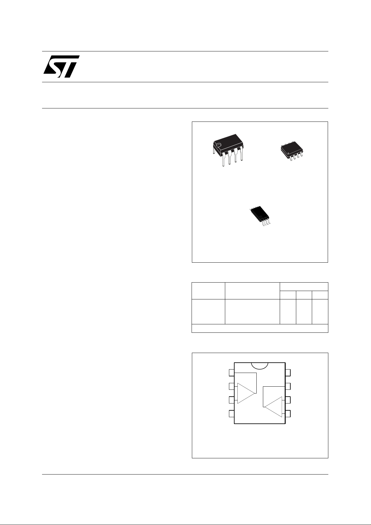
LM358,A
N
DIP8
(Plast ic Pac kag e)
(Thin Shrink Small Outline Package)
(Plastic Micropackage)
P
TSSOP8
D
SO8
DESCRIPTION
These circuits co nsist of two independent, high ga in,
internally frequency compensated which were
designed spec ifically to opera te from a single p ower
supply over a wide range of volt ages. The low power
supply drain is in dependent of the magnit ude o f the
power supply voltage.
Application areas include transducer amplifiers, dc
gain blo cks and all the conv entiona l op-amp c ircuit s
which now can be mor e easily implemented in s ingle
power supply systems. For example, these circuits
can be directly supplied with the standard + 5V
which is used in logic systems and will easily provide
the required interface electronics without requiring
any additional pow er su pply .
In the linear mode the input common-mode voltage
range includes ground and the output voltage can
also swing to ground, even though operated from
only a sin gle po wer supp l y volt ag e.
ORDER CODES
Part
Number
LM158,A –55
LM258,A –40
LM358,A 0
Example : LM258N
PIN CONNECTIONS (top view)
1 - Output 1
2 - Inverting input 1
3 - Non-inver ti ng inpu t 1
-
4 - V
CC
Temperature
Range
o
C, +125oC •••
o
C, +105oC •••
o
C, +70oC •••
1
2
-
+
3
45
-
+
5 - Non-inverting input 2
6 - Inverting input 2
7 - Ouput 2
8 - V
CC
Package
NDP
8
7
6
+
June 1998
1/12
LM158,A - L M258,A - L M358,A
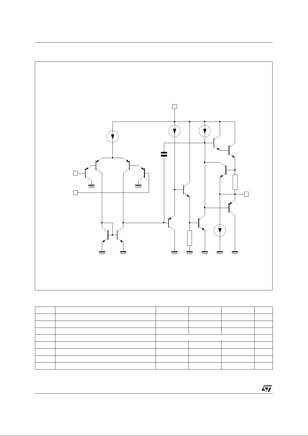
SCHEMATIC DIAGRAM (1/2 LM158)
V
CC
Inverting
input
Non-inverting
input
Q2
Q8 Q9
6µA
Q3
4µA
C
C
Q4Q1
100µA
Q5
Q7
Q6
R
SC
Q11
Output
Q13
Q10
Q12
50µA
GND
ABSOLUTE MAXIMUM RATINGS
Symbol Parameter LM158,A LM258,A LM358,A Unit
V
T
2/12
Supply Voltage +32 +32 +32 V
CC
Input Voltage –0.3 to +32 –0.3 to +32 –0.3 to +32 V
V
i
Differential Input Voltage +32 +32 +32 V
V
id
Output Short-circuit Duration - (note 2) Infinite
Power Dissipation 500 500 500 mW
P
tot
I
Input Current - (note 1) 50 50 50 mA
in
Operating Free-air Temperature Range –55 to +125 –40 to +105 0 to +70
oper
Storage Temperature Range –65 to +150 –65 to +150 –65 to +150
T
stg
o
C
o
C
ELECTRICAL CHARACTERISTICS
V
CC
+
= +5V, V
–
= Ground, VO = 1.4V, T
CC
Symbol Parameter
V
A
SVR Supply Voltage Rejection Ratio (R
I
V
Input Offset Voltage - (note 3)
I
I
CC
io
io
ib
vd
icm
T
= 25oC
amb
≤ T
≤ T
T
min.
amb
max
.
Input Offset Current
= 25oC
T
amb
T
≤ T
≤ T
min.
amb
max
.
Input Bias Current - (note 4)
T
= 25oC
amb
T
≤ T
≤ T
min.
amb
max
.
Large Signal Voltage Gain
(VCC = +15V, RL = 2kΩ, VO = 1.4V to 11.4V)
T
= 25oC
amb
≤ T
≤ T
≤ T
max
max
.
.
(V
CC
T
min.
+
= 5 to 30V)
T
= 25oC
amb
T
≤ T
min.
amb
amb
Supply Current, all Amp, no Load
VCC = +5V, T
VCC = +30V, T
min.
min.
≤ T
≤ T
amb
amb
Input Common Mode Voltage Range
(VCC = +30V) - (note 6)
= 25oC
T
amb
T
. ≤ T
≤ T
min
amb
max
.
CMR Common-mode Rejection Ratio (R
= 25oC
T
amb
T
≤ T
≤ T
min.
I
source
I
V
V
V
Output Current Source
(VCC = +15V, Vo = 2V, Vid = +1V) 20 40 60 20 40 60
Output Current Sink (Vid = -1V)
sink
OPP
OH
OL
= +15V, VO = 2V
V
CC
VCC = +15V, VO = +0.2V
Output Voltage Swing (RL = 2kΩ)
T
= 25oC
amb
≤ T
T
min.
High Level Output Voltage (V
T
= 25oCR
amb
T
. ≤ T
min
= 25oCR
T
amb
T
≤ T
min.
Low Level Output Voltage (RL = 10kΩ)
T
= 25oC
amb
. ≤ T
T
min
SR Slew Rate (V
2kΩ, CL = 100pF, unity gain) 0.3 0.6 0.3 0.6
amb
amb
amb
amb
amb
CC
.
max
≤ T
.
max
≤ T
.
max
≤ T
.
max
≤ T
max.
= 15V, VI = 0.5 to 3V, RL =
GBP Gain Bandwidth Product
(V
= 30V, f = 100kHz,
CC
= 10mV, RL = 2kΩ, CL = 100pF) 0.7 1.1 0.7 1.1
V
in
THD Total Harmonic Distortion
(f = 1kHz, A
= 100pF, VO = 2 PP)
C
L
e
Equivalent Input Noise voltage
n
(f = 1kHz, R
= 20dB, RL = 2kΩ, VCC = 30V,
v
= 100Ω, VCC = 30V) 55 55
s
amb
LM158, LM258
LM158A
LM158, LM258
= 10kΩ)
S
≤ T
.
max
≤ T
.
max
= 10kΩ)
S
+
= 30V)
CC
= 2kΩ
L
= 10kΩ
L
LM158,A - LM258,A - LM358,A
= 25oC (unless otherwise specified)
LM158A-LM258A
LM358A
Min. Typ. Max. Min. Typ. Max.
13
2
4
210
30
20 50
100
5025100 5025100
6565100 6565100
0.7 1.2
2
0
0
V
CC
V
CC
+
–1.5
+
–200
706085 706085
101220
50
V
CC
V
CC
+
–1.5
+
–200
26
0
0
27
26
27
28
27
520
20
0.02 0.02
LM158-LM258
101220
26
26
27
27
LM358
27
5
9
7
230
40
20 150
200
0.7 1.2
2
+
V
–1.5
CC
+
V
–2
CC
50
+
V
–1.5
CC
+
–2
V
CC
27
28
520
20
Unit
mV
nA
nA
V/mV
dB
mA
V
dB
mA
mA
µA
V
V
mV
V/µs
MHz
%
nV
√Hz
3/12
LM158,A - L M258,A - L M358,A
ELECTRICAL CHARACTERISTICS (continued)
LM158A
Symbol Parameter
LM258A
LM358A
Min. Typ. Max. Min. Typ. Max.
DV
DI
V
O1/VO2
Notes : 1. This input current only exist when the voltage at any of the input leads is driven negative. It is due to the collec-
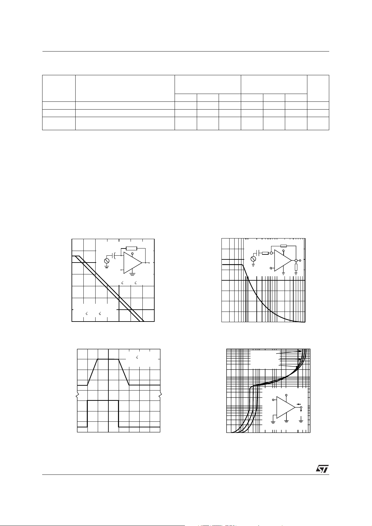
OPEN LOOP FREQUENCY RESPONSE
Input Offset Voltage Drift 7 15 7 30 µV/oC
io
Input Offset Current Drift 10 200 10 300 pA/oC
io
Channel Separation (note 5)
1kHz ≤ f ≤ 20kHz 120 120
tor-base junction of the i nput PNP transi stor becoming fo rward biased and thereby acti ng as input d iode clamps.
In addition to this di ode action, there is also NPN parasitic action on the IC chip. This transistor action can cause
the output voltages of the Op-amps to go to the V
duration that an input is driven negative.
This is not destructive and normal output will set up again for input voltage higher than –0.3V.
2. Short-circuits from the output to V
can cause excessive heating if V
CC
approximatively 40mA independent of the magnitude of V
short-circuits on all amplifiers.
3. V
= 1.4V, RS = 0Ω, 5V < V
O
+
< 30 V, 0 < Vic < V
CC
4. The direction of the input current is out of the IC. This current is essentially constant, independent of the state of
the output so no loading change exists on the input lines.
5. Due to the proximity of external components insure that coupling is not originating via stray capacitance between
these external parts. T his typically can be detec ted as this typ e of capacitan ce increases at higher freque nces.
6. The input common-mode voltage of either input signal voltage should not be allowed to go negative by more than
0.3V. The upper end of the common-mode voltage range is V
But either or both inputs can go to +32V without damage.
(NOTE 3)
140
10M
120
100
0.1mF
V
I
VCC/2
80
VCC = 30V &
60
-55°C
W
V
-
CC
V
O
+
T
+125°C
amb
voltage level (or to ground for a large overdrive) for the time
CC
+
> 15V. The maximum output current is
+
– 1.5V.
CC
+
– 1.5V.
CC
. Destructive dissipation can result from simultaneous
CC
CC
LARGE SIGNAL FREQUENCY RESPONSE
20
15
10
V
LM158
LM258
LM358
Unit
dB
100k
1k
W
I
+7V
W
+15V
-
+
VO
2k
W
40
VOLTAGE GAIN (dB)
20
0
1.0 10 100 1k 10k 100k 1M 10M
VOLAGE FOLLOWER PULSE RESPONSE
4
3
2
OUTPUT
1
VOLTAGE (V)
0
3
2
1
INPUT
VOLTAGE (V)
4/12
VCC = +10 to + 15V &
T
amb
+125°C
-55°C
FREQUENCY (Hz)
RL 2 k
W
VCC = +15V
010203040
TIME (ms)
5
OUTPUT SWING (Vpp)
0
1k 10k 100k 1M
FREQUENCY (Hz)
OUTPUT CHARACTERISTICS
10
1
0.1
OUTPUT VOLTAGE (V)
0.01
0,001 0,01 0,1 1 10 100
VCC = +5V
VCC = +15V
VCC = +30V
vcc/2
T
-
+
amb
v
cc
= +25°C
OUTPUT SINK CURRENT (mA)
I
O
V
O
 Loading...