

SGS Thomson Microelectronics LM317P, LM317K, LM317D2T, LM217T, LM217K Datasheet
...
LM117/217
LM317
1.2V TO 37V VOLTAGE REGULATOR
November 1999
■ OUTPUT VOLTAGERANGE: 1.2TO 37V
■ OUTPUT CURRENT INEXCESS OF 1.5A
■ 0.1%LINE AND LOADREGULATION
■ FLOATINGOPERATION FOR HIGH
VOLTAGES
■ COMPLETESERIESOF PROTECTIONS:
CURRENTLIMITING,THERMAL
SHUTDOWNANDSOA CONTROL
DESCRIPTION
The LM117/LM217/LM317 are monolithic
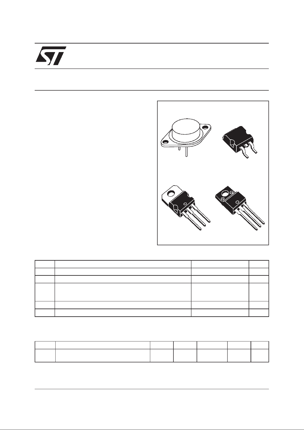
integrated circuit in TO-220, ISOWATT220, TO-3
and D
2
PAK packages intended for use as
positiveadjustable voltageregulators.
They are designed to supply more than 1.5A of
load current with an output voltage adjustable
overa 1.2 to 37V range.
The nominal output voltage is selected by means
of only a resistive divider, making the device
exceptionally easy to use and eliminating the
stockingof manyfixed regulators.
TO-3
TO-220
D
2
PAK
ABSOLUTE MAXIMUMRATING
Symbol Parameter Value Unit
V
i-o
Input-output Differential Voltage 40 V
I
O
OutputCurrent Intenrally Limited
T
op
OperatingJunction Temperaturefor:LM117
LM217
LM317
-55 to 150
-25 to 150
0 to 125
o
C
o
C
o
C
P
tot
PowerDissipation Internally Limited
T
stg
StorageTemperature - 65 to 150
o
C
THERMALDATA
Symbol Parameter TO-3 TO-220 ISOWATT220 D2PAK Unit
R
thj-cas e
R
thj-amb
Thermal Resistance Junction-case Max
Thermal Resistance Junction-ambient Max
4
35
3
50
4
60
3
62.5
o
C/W
o
C/W
ISOWATT220
1/11
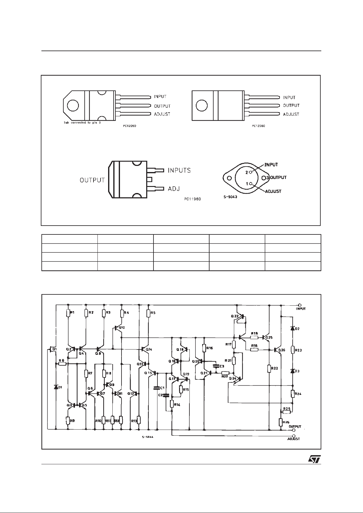
CONNECTION DIAGRAM ANDORDERING NUMBERS
(top view)
TO-220
D
2
PAK TO-3
Type TO-3 TO-220 ISOWATT220 D
2
PAK
LM117 LM117K
LM217 LM217K LM217T LM217D2T
LM317 LM317K LM317T LM317P LM317D2T
SCHEMATIC DIAGRAM
ISOWATT220
LM117/217/317
2/11
BASIC ADJUSTABLE REGULATOR
ELECTRICAL CHARACTERISTICS (V
i-Vo
= 5V, Io=500 mA, I
MAX
= 1.5Aand P
MAX
= 20W,unless
otherwisespecified)
Symbol Parameter Test Conditions LM117/LM217 LM317 Unit
Min. Typ. Max. Min. Typ. Max.
∆V
o
LineRegulation Vi-Vo= 3 to40 V Tj=25oC 0.01 0.02 0.01 0.04 %/V
0.02 0.05 0 . 02 0. 07 %/V
∆V
o
LoadRegulation
V
o
≤ 5V
I
o
=10mAtoI
MAX
Tj=25oC515 525mV
20 50 20 70 mV
V
o
≥
5V
I
o
=10mAtoI
MAX
Tj=25oC 0.1 0.3 0.1 0 .5 %
0.3 1 0.3 1.5 %
I
ADJ
Adjustment Pin Current 50 100 50 100
µ
A
∆
I
ADJ
Adjustment Pin Current Vi-Vo= 2.5 to 40V
I
o
=10mAtoI
MAX
0.2 5 0.2 5
µ
A
V
REF
Reference Voltage
(between pin3 andpin
1)
Vi-Vo= 2.5 to 40V
I
o
=10mAtoI
MAX
P
D
≤
P
MAX
1.21.251.3 1.21.251.3 V
∆
V
o
V
o
OutputVoltage
Temperature Stability
11%
I
o(min)
MinimumLoad Current Vi-Vo= 40V 3.5 5 3.5 10 mA
I
o(max)
Maximum Load
Current
V
i-Vo
≤
15 V
P
D<PMAX
1.52.2 1.52.2 A
V
i-Vo
=40V
P
D<PMAX
Tj=25oC
0.4 0.4 A
e
N
OutputNoise Voltage
(percentance of V
O
)
B= 10Hz to 10KHz
Tj=25oC
0.003 0.003 %
SVR Supply Voltage
Rejection(*)
T
j
=25oC
f =120 Hz
C
ADJ
=0 65 65 dB
C
ADJ
=10µF
66 80 66 80 dB
(*) CADJ is connected between pin 1 and ground.
Note:
(1) Unless otherwisespecified the above specs, apply over the following conditions :LM 117 T
j
= –55 to 150°C;
LM 217 T
j
= –25 to 150°C ; LM317 Tj= 0to 125°C.
LM117/217/317
3/11
APPLICATION INFORMATION
The LM117/217/317 provides an internal
reference voltage of 1.25V between the output
and adjustments terminals. This is used to set a
constant current flow across an external resistor
divider(see fig. 4),giving an outputvoltage V
O
of:
V
O=VREF
(1 +
R
2
R
1
) +I
ADJR2
The device was designed to minimize the term
I
ADJ
(100µA max) and to maintainit very constant
with line and load changes. Usually, the error
term I
ADJ
⋅ R2can be neglected. To obtain the
previous requirement, all the regulator quiescent
current is returned to the output terminal,
imposinga minimum load current condition.If the
load is insufficient, the output voltagewill rise.
Since the LM117/217317 is a floating regulator
and ”sees” only the input-to-output differential
voltage,supplies of very highvoltage withrespect
to ground can be regulated as long as the
maximum input-to-output differential is not
exceeded. Furthermore, programmable regulator
are easily obtainable and, by connecting a fixed
resistor between the adjustment and output, the
device can be used as a precision current
regulator.
In order to optimise the load regulation, the
current set resistor R1 (see fig. 4) should be tied
as close as possible to the regulator, while the
ground terminal of R2 should be near the ground
of theload to provideremote ground sensing.
Performance may be improved with added
capacitanceas follow:
Aninput bypass capacitorof 0.1µF
An adjustment terminal to ground 10µF capacitor
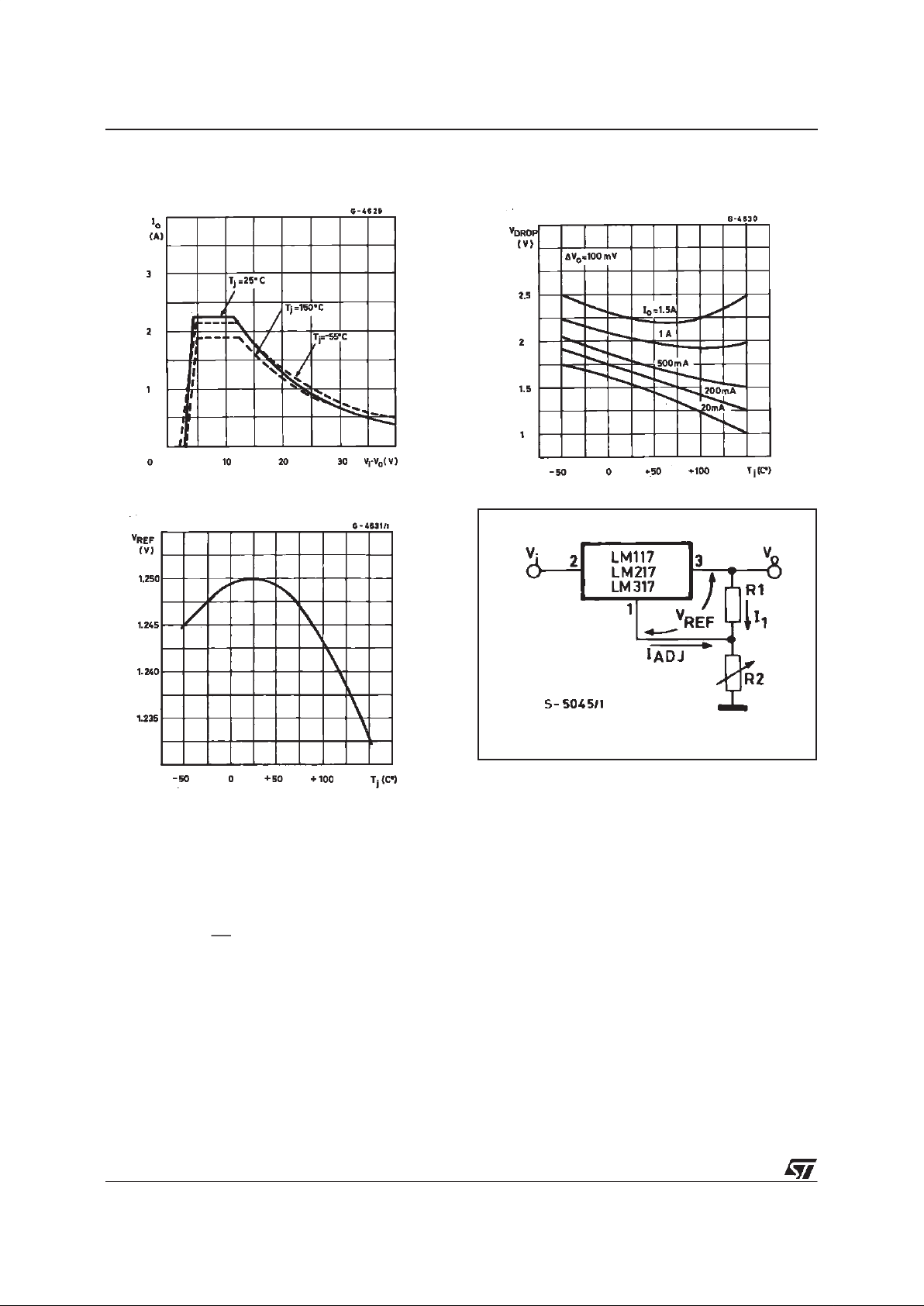
Figure4 : Basic AdjustableRegulator.
Figure1 :
OutputCurrent vs. Input-output
DifferentialVoltage.
Figure2 :
DropoutVoltage vs. Junction
Temperature.
Figure3 : ReferenceVoltage vs.Junction
LM117/217/317
4/11
 Loading...