


Ordering number : ENN7070
Thick-Film Hybrid IC
STK402-240
Three-Channel Class AB Audio Power Amplifier IC 25 W + 25 W + 25 W
Overview
The STK402-200 series products are audio power amplifier hybrid ICs that consist of optimally-designed discrete component power amplifier circuits that have been miniaturized using SANYO's unique insulated metal substrate technology (IMST). SANYO has adopted a new low thermal resistance substrate in these products to reduce the package size by about 60% as compared to the earlier SANYO STK408-000 series.
Features
•Series of pin compatible power amplifiers ranging from 20 W × 3 channels to 60 W × 3 channels (10%/1 kHz)
devices. The same printed circuit board can be used depending on the output power grade.
•The pin arrangement is compatible with that of the 2- channel STK402-000 series. This means that 3-channel printed circuit boards can also be used for 2-channel products.
•Miniature packages
—15 W/ch to 40 W/ch (THD = 0.4%, f = 20 Hz to 20 kHz); 59.2 mm × 31.0 mm × 8.5 mm *
*: Not including the pins.
•Achieves superlative heat dissipation due to the adoption of SANYO's Insulated Metal Substrate Technology (IMST).
•Output load impedance: RL = 6 Ω
•Allowable load shorted time: 0.3 seconds
•Supports the use of standby, muting, and load shorting protection circuits.
Package Dimensions
unit: mm
4191-SIP19 |
[STK402-240] |
SANYO: SIP19 |
 Any and all SANYO products described or contained herein do not have specifications that can handle applications that require extremely high levels of reliability, such as life-support systems, aircraft’s control systems, or other applications whose failure can be reasonably expected to result in serious physical and/or material damage. Consult with your SANYO representative nearest you before using any SANYO products described or contained herein in such applications.
 SANYO assumes no responsibility for equipment failures that result from using products at values that exceed, even momentarily, rated values (such as maximum ratings, operating condition ranges, or other parameters) listed in products specifications of any and all SANYO products described or contained herein.
SANYO Electric Co.,Ltd. Semiconductor Company
TOKYO OFFICE Tokyo Bldg., 1-10, 1 Chome, Ueno, Taito-ku, TOKYO, 110-8534 JAPAN
N1102AS (OT) No. 7070-1/4
STK402-240
Series Organization
These products are organized as a series based on their output capacity.
Item |
|
|
Type No. |
|
|
|
|
|
|
|
|
||
STK402-220 |
STK402-230 |
STK402-240 |
STK402-250 |
STK402-270 |
||
|
||||||
|
|
|
|
|
|
|
Output 1 (10%/1 kHz) |
20 W + 20 W + 20 W |
30 W + 30 W + 30 W |
40 W + 40 W + 40 W |
45 W +45 W +45 W |
60 W + 60 W + 60 W |
|
|
|
|
|
|
|
|
Output 2 (0.4%/20 Hz to 20 kHz) |
15 W + 15 W + 15 W |
20 W + 20 W + 20 W |
25 W + 25 W + 25 W |
30 W + 30 W + 30 W |
40 W + 40 W + 40 W |
|
|
|
|
|
|
|
|
Maximum supply voltage |
±30 V |
±34 V |
±38 V |
±40 V |
±50 V |
|
(No signal) |
||||||
|
|
|
|
|
||
|
|
|
|
|
|
|
Maximum supply voltage |
±28 V |
±32 V |
±36 V |
±38 V |
±44 V |
|
(6 Ω ) |
||||||
|
|
|
|
|
||
|
|
|
|
|
|
|
Recommended supply voltage |
±19 V |
±22 V |
±25 V |
±26.5 V |
±30 V |
|
(6 Ω ) |
||||||
|
|
|
|
|
||
|
|
|
|
|
|
|
Package |
|
59.2 mm × 31.0 mm × 8.5 mm |
|
|||
|
|
|
|
|
|
|
Specifications
Maximum Ratings at Ta = 25°C
Parameter |
|
Symbol |
|
|
|
Conditions |
|
|
Ratings |
|
Unit |
||||
|
|
|
|
|
|
|
|
|
|
|
|
|
|
|
|
Maximum supply voltage (No signal) |
|
VCC max(1) |
|
|
|
|
|
|
|
±38 |
|
V |
|||
Maximum supply voltage |
|
VCC max(2) |
RL = 6 Ω , 8 Ω |
|
|
|
|
|
±36 |
|
V |
||||
Thermal resistance |
|
θj-c |
|
Per power transistor |
|
|
|
3.5 |
|
°C/W |
|||||
|
|
|
|
|
|
|
|
|
|
|
|
|
|
|
|
Junction temperature |
|
Tj max |
Both the Tj max and the Tc max conditions must be met. |
|
150 |
|
°C |
||||||||
|
|
|
|
|
|
|
|
|
|
||||||
Operating IC substrate temperature |
|
Tc max |
|
125 |
|
°C |
|||||||||
|
|
|
|
|
|
|
|
|
|||||||
|
|
|
|
|
|
|
|
|
|
|
|
|
|
|
|
Storage temperature |
|
Tstg |
|
|
|
|
|
|
|
–30 to +125 |
|
°C |
|||
|
|
|
|
|
|
|
|
|
|
|
|
|
|
|
|
Allowable load shorted time *2 |
|
ts |
|
VCC = ±25 V, RL = 6 Ω , Tc = 25°C, f = 50 Hz, PO = 25 W, 1ch drive |
|
0.3 |
|
s |
|||||||
Operating Characteristics at Tc = 25°C, RL = 6 Ω (noninductive load), Rg = 600 Ω , VG = 30 dB |
|
|
|
||||||||||||
|
|
|
|
|
|
|
|
|
|
|
|
|
|
|
|
Parameter |
|
Symbol |
|
|
|
|
Conditions*1 |
|
|
Ratings |
|
|
Unit |
||
|
|
VCC (V) |
f (Hz) |
PO (W) |
THD (%) |
|
min |
typ |
max |
|
|||||
|
|
|
|
|
|
|
|
||||||||
|
|
PO (1) |
|
±25.0 |
20 to 20 k |
|
0.4 |
|
25 |
|
|
|
|
||
Output power |
|
PO (2) |
|
±25.0 |
1 k |
|
10 |
|
|
40 |
|
|
W |
||
|
|
PO (3) |
|
±25.0 |
20 to 20 k |
|
0.4 |
at 8 Ω |
|
23 |
|
|
|
||
Total harmonic distortion |
|
THD (1) |
|
±25.0 |
20 to 20 k |
1.0 |
|
|
|
|
0.4 |
|
% |
||
|
|
|
|
|
|
|
|
|
|
|
|
|
|
||
|
THD (2) |
|
±25.0 |
1 k |
5.0 |
|
|
|
0.01 |
|
|
||||
|
|
|
|
|
|
|
|
|
|||||||
|
|
|
|
|
|
|
|
|
|
|
|
|
|
||
Frequency characteristics |
|
fL, fH |
|
±25.0 |
|
1.0 |
|
+0 –3 dB |
|
20 to 50 k |
|
|
Hz |
||
Input impedance |
|
ri |
|
±25.0 |
1 k |
1.0 |
|
|
|
55 |
|
|
kΩ |
||
|
|
|
|
|
|
|
|
|
|
|
|
|
|
||
Output noise voltage *3 |
|
VNO |
|
±30.0 |
|
|
|
Rg = 2.2 kΩ |
|
|
1.2 |
|
mVrms |
||
Quiescent current |
|
ICCO |
|
±30.0 |
|
|
|
|
10 |
60 |
110 |
|
mA |
||
Neutral voltage |
|
VN |
|
±30.0 |
|
|
|
|
–70 |
0 |
+70 |
|
mV |
||
Notes: 1. Unless otherwise noted, use a constant-voltage supply for the power supply used during inspection.
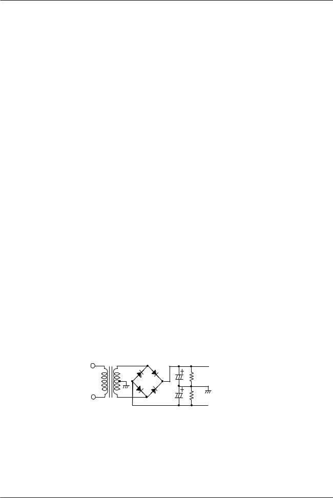
2.Use the transformer power supply circuit stipulated in the figure below for allowable load shorted time measurement and output noise voltage measurement.
DBA40G |
4700 µF |
 +VCC
+VCC
500 Ω
500 Ω
 --VCC
--VCC
4700 µF
Stipulated Transformer Power Supply (RP-25 equivalent)
3.The output noise voltage values shown are peak values read with a VTVM. However, an AC stabilized (50 Hz) power supply should be used to minimize the influence of AC primary side flicker noise on the reading.
No. 7070-2/4
 Loading...