


Ordering number:ENN5170
Thick Film Hybrid IC
STK392-110
3-Channel Convergence Correction Circuit
(IC max = 3A)
Overview
The STK392-110 is a convergence correction circuit IC for video projectors. It incorporates three output amplifiers in a single package, making possible the construction of CRT horizontal and vertical convergence correction output circuits for each of the RGB colors using ust two hybrid ICs. The output circuit use a class-B configuration, in comparison with the STK392-010, realizing a more compact package and lower cost.
Applications
• Video projectors
Features
•3 output amplifier circuits in a single package
•High maximum supply voltage (VCC max = ±38V)
•Low thermal resistance (θj-c=3.0°C/W)
•High temperature stability (TC max=125°C)
•Separate predriver and output stage supplies
•Output stage supply switching for high-performance designs
•Low inrush current when power is applied
Package Dimensions
unit:mm |
|
|
|
|
|
|
4083 |
|
|
|
|
|
|
|
|
[STK392-110] |
|
|
|
|
|
|
64.0 |
|
|
|
|
|
|
55.6 |
|
|
|
8.5 |
3.6 |
|
|
|
31.0 |
|
|
|
|
16.5 |
21.0 |
25.8 |
|
|
1 |
|
18 |
|
|
|
2.9 |
|
|
|
|
|
|
|
(6.21) |
2.54 |
0.5 |
|
|
4.0 |
0.4 |
17×2.54=43.18 |
|
|
|
5.5 |
||
|
|
|
|
|
SANYO : SIP18 |
|
Series Organization
The following devices form a series with varying output capacity and application grade. Some of the devices below are under development, so contact your nearest sales representative for details.
Type No. |
|
Maximum ratings |
|
Maximum horizontal frequency |
Application grade |
|
|
VCC max |
IC max |
|
θj-c |
fH max |
|
STK392-110 |
±38V |
3A |
|
3.0˚C/W |
15kHz |
General projection TVs |
|
|
|
|
|
|
|
STK392-010 |
±38V |
5A |
|
2.6˚C/W |
15kHz |
General projection TVs |
|
|
|
|
|
|
|
STK392-020 |
±44V |
6A |
|
2.1˚C/W |
35kHz |
HD, VGA |
|
|
|
|
|
|
|
STK392-040 |
±50V |
7A |
|
1.8˚C/W |
100kHz |
XGA, CAD, CAM |
|
|
|
|
|
|
|
STK392-210 |
±65V |
8A |
|
1.5˚C/W |
130kHz |
CAD, CAM |
|
|
|
|
|
|
|
STK392-220 |
±75V |
10A |
|
1.3˚C/W |
160kHz |
CAD, CAM |
|
|
|
|
|
|
|
 Any and all SANYO products described or contained herein do not have specifications that can handle applications that require extremely high levels of reliability, such as life-support systems, aircraft’s control systems, or other applications whose failure can be reasonably expected to result in serious physical and/or material damage. Consult with your SANYO representative nearest you before using any SANYO products described or contained herein in such applications.
 SANYO assumes no responsibility for equipment failures that result from using products at values that exceed, even momentarily, rated values (such as maximum ratings, operating condition ranges,or other parameters) listed in products specifications of any and all SANYO products described or contained herein.
SANYO Electric Co.,Ltd. Semiconductor Company
TOKYO OFFICE Tokyo Bldg., 1-10, 1 Chome, Ueno, Taito-ku, TOKYO, 110-8534 JAPAN
93099TH (KT)/80995HA (ID) No.5170–1/4

STK392-110
Specifications
Maximum Ratings at Ta = 25˚C
Parameter |
Symbol |
Conditions |
Ratings |
Unit |
|
|
|
|
|
Maximum supply voltage |
VCC max |
|
±38 |
V |
Maximum collector current |
IC |
Tr6, 7, 13, 14, 20, 21 |
3.0 |
A |
Thermal resistance |
θ j-c |
Tr6, 7, 13, 14, 20, 21 (per transistor) |
3.0 |
˚C/W |
Junction temperature |
Tj |
|
150 |
˚C |
|
|
|
|
|
Operating temperature |
Tc |
|
125 |
˚C |
|
|
|
|
|
Storage temperature |
Tstg |
|
–30 to +125 |
˚C |
|
|
|
|
|
Operating Characteristics at Ta = 25˚C, Rg=50Ω, VCC=±30V, specified test circuit
Parameter |
Symbol |
Conditions |
|
Ratings |
|
Unit |
|
|
|
||||
|
|
|
min |
typ |
max |
|
|
|
|
|
|
|
|
Output noise voltage |
VNO |
|
|
|
0.2 |
mVrms |
Quiescent current |
ICCO |
|
15 |
22 |
30 |
mA |
Neutral voltage |
VN |
|
–50 |
0 |
+50 |
mV |
Output delay time |
tD |
f=15.75kHz, triangular wave input, VOUT=1.5Vp-p |
|
|
1 |
µs |
Note :
All tests are conducted using a constant-voltage regulated supply unless otherwise specified.
The output noise voltage is the peak value of an average-reading meter with an rms value scale (VTVM).
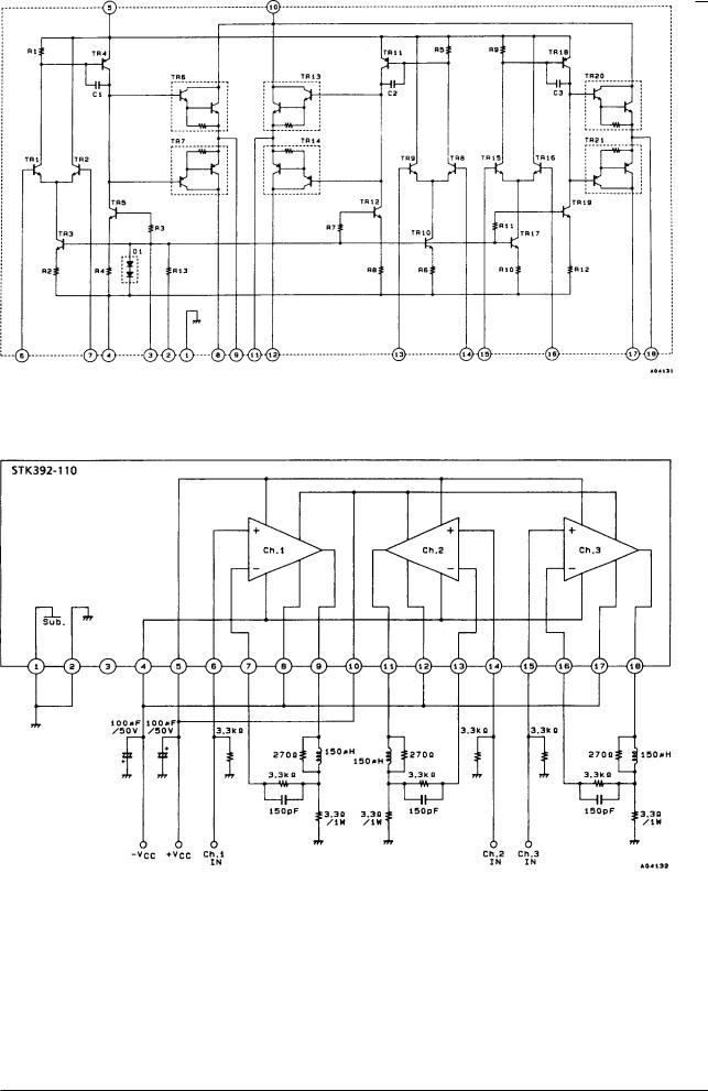
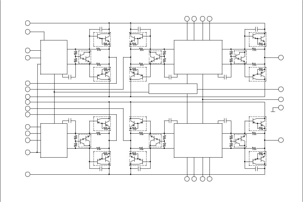
Block Diagram
No.5170–2/4
STK392-110
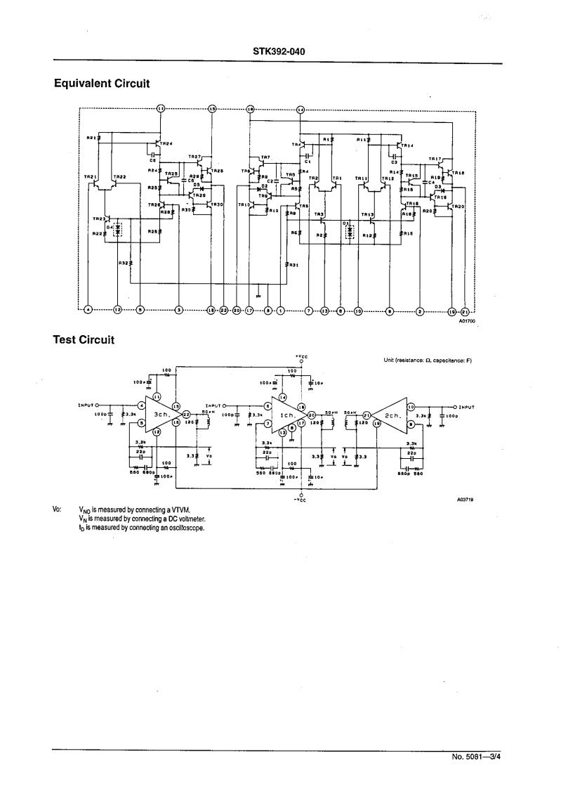
Equivalent Circuit
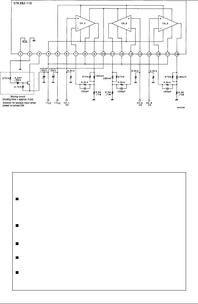
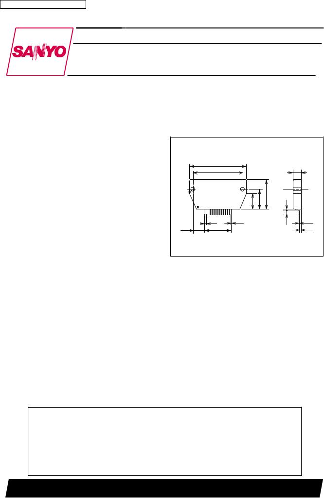
Test Circuit
No.5170–3/4
STK392-110
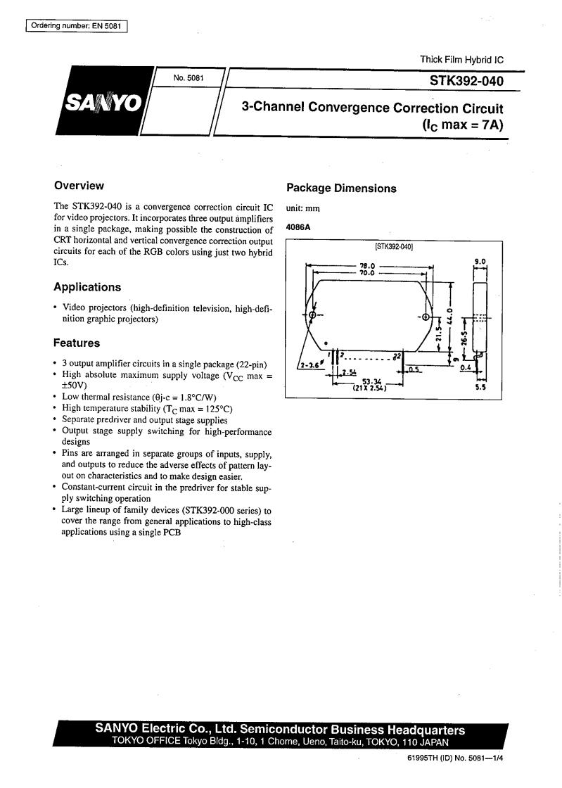
Sample Application Circuit
 Specifications of any and all SANYO products described or contained herein stipulate the performance, characteristics, and functions of the described products in the independent state, and are not guarantees of the performance, characteristics, and functions of the described products as mounted in the customer's products or equipment. To verify symptoms and states that cannot be evaluated in an independent device, the customer should always evaluate and test devices mounted in the customer's products or equipment.
SANYO Electric Co., Ltd. strives to supply high-quality high-reliability products. However, any and all semiconductor products fail with some probability. It is possible that these probabilistic failures could give rise to accidents or events that could endanger human lives, that could give rise to smoke or fire, or that could cause damage to other property. When designing equipment, adopt safety measures so that these kinds of accidents or events cannot occur. Such measures include but are not limited to protective circuits and error prevention circuits for safe design, redundant design, and structural design.
In the event that any or all SANYO products(including technical data,services) described or contained herein are controlled under any of applicable local export control laws and regulations, such products must not be exported without obtaining the export license from the authorities concerned in accordance with the above law.
No part of this publication may be reproduced or transmitted in any form or by any means, electronic or mechanical, including photocopying and recording, or any information storage or retrieval system, or otherwise, without the prior written permission of SANYO Electric Co., Ltd.
Any and all information described or contained herein are subject to change without notice due to product/technology improvement, etc. When designing equipment, refer to the "Delivery Specification" for the SANYO product that you intend to use.
Information (including circuit diagrams and circuit parameters) herein is for example only ; it is not guaranteed for volume production. SANYO believes information herein is accurate and reliable, but no guarantees are made or implied regarding its use or any infringements of intellectual property rights or other rights of third parties.
This catalog provides information as of September, 1999. Specifications and information herein are
subject to change without notice.
PS No.5170–4/4

Ordering number : ENN7065A
Thick-Film Hybrid IC
STK402-090
Two-Channel Class AB Audio Power Amplifier IC 50 W + 50 W
Overview
The STK402-000 series products are audio power amplifier hybrid ICs that consist of optimally-designed discrete component power amplifier circuits that have been miniaturized using SANYO's unique insulated metal substrate technology (IMST). SANYO has adopted a new low thermal resistance substrate in these products to reduce the package size by about 60% as compared to the earlier SANYO STK407-000 series.
Features
•Series of pin compatible power amplifiers ranging from 20 W × 2 channels to 120 W × 2 channels (10%/1 kHz)
devices. The same printed circuit board can be used depending on the output power grade.
•The pin arrangement is compatible with that of the 3- channel STK402-200 series. This means that 3-channel printed circuit boards can also be used for 2-channel products.
•Miniature packages
—15 W/ch to 40 W/ch (THD = 0.4%, f = 20 Hz to 20 kHz); 46.6 mm × 25.5 mm × 8.5 mm *
—50 W/ch to 80 W/ch (THD = 0.4%, f = 20 Hz to 20 kHz); 59.2 mm × 31.0 mm × 8.5 mm *
*: Not including the pins.
•Output load impedance: RL = 6 Ω
•Allowable load shorted time: 0.3 seconds
•Supports the use of standby, muting, and load shorting protection circuits.
Package Dimensions
unit: mm
4190-SIP15 |
|
|
|
|
|
|
|
|
[STK402-090] |
|
|
|
|
|
59.2 |
|
|
|
|
|
|
52.0 |
|
|
|
|
8.5 |
ø3.6 |
|
|
|
31.0 |
|
|
|
|
16.5 |
21.0 |
1.0 |
|
|
1 |
|
15 |
|
|
|
|
|
2.0 |
0.5 |
|
|
4.0 |
0.4 |
(12) |
14X2=28 |
|
|
|
|
2.9 |
|
|
|
|
|
SANYO: SIP15 |
|
 Any and all SANYO products described or contained herein do not have specifications that can handle applications that require extremely high levels of reliability, such as life-support systems, aircraft’s control systems, or other applications whose failure can be reasonably expected to result in serious physical and/or material damage. Consult with your SANYO representative nearest you before using any SANYO products described or contained herein in such applications.
 SANYO assumes no responsibility for equipment failures that result from using products at values that exceed, even momentarily, rated values (such as maximum ratings, operating condition ranges, or other parameters) listed in products specifications of any and all SANYO products described or contained herein.
SANYO Electric Co.,Ltd. Semiconductor Company
TOKYO OFFICE Tokyo Bldg., 1-10, 1 Chome, Ueno, Taito-ku, TOKYO, 110-8534 JAPAN
D0102AS (OT) No. 7065-1/5
STK402-090
Series Organization
These products are organized as a series based on their output capacity.
Item |
|
|
|
Type No. |
|
|
|
||
|
|
|
|
|
|
|
|
||
STK402-020 |
STK402-030 |
STK402-040 |
STK402-050 |
STK402-070 |
STK402-090 |
STK402-100 |
STK402-120 |
||
|
|||||||||
|
|
|
|
|
|
|
|
|
|
Output 1 (10%/1 kHz) |
20 W + 20 W |
30 W + 30 W |
40 W + 40 W |
45 W +45 W |
60 W + 60 W |
80 W + 80 W |
100 W + 100 W |
120 W + 120 W |
|
|
|
|
|
|
|
|
|
|
|
Output 2 (0.4%/20 Hz to 20 kHz) |
15 W + 15 W |
20 W + 20 W |
25 W + 25 W |
30 W + 30 W |
40 W + 40 W |
50 W + 50 W |
60 W + 60 W |
80 W + 80 W |
|
|
|
|
|
|
|
|
|
|
|
Maximum supply voltage |
±30 V |
±34 V |
±38 V |
±40 V |
±50 V |
±54 V |
±57 V |
±65 V |
|
(No signal) |
|||||||||
|
|
|
|
|
|
|
|
||
|
|
|
|
|
|
|
|
|
|
Maximum supply voltage |
±28 V |
±32 V |
±36 V |
±38 V |
±44 V |
±47 V |
±50 V |
±57 V |
|
(6 Ω ) |
|||||||||
|
|
|
|
|
|
|
|
||
|
|
|
|
|
|
|
|
|
|
Recommended supply voltage |
±19 V |
±22 V |
±25 V |
±26.5 V |
±30 V |
±32 V |
±35 V |
±39 V |
|
(6 Ω ) |
|||||||||
|
|
|
|
|
|
|
|
||
|
|
|
|
|
|
|
|
|
|
Package |
|
46.6 mm × 25.5 mm × 8.5 mm |
|
59.2 mm × 31.0 mm × 8.5 mm |
|||||
|
|
|
|
|
|
|
|
|
|
Specifications
Maximum Ratings at Ta = 25°C
Parameter |
|
Symbol |
|
|
|
|
Conditions |
|
Ratings |
|
Unit |
||||
|
|
|
|
|
|
|
|
|
|
|
|
|
|
|
|
Maximum supply voltage (No signal) |
|
VCC max(0) |
|
|
|
|
|
|
|
|
±54 |
|
V |
||
Maximum supply voltage |
|
VCC max(1) |
RL = 6 Ω |
|
|
|
|
|
|
±47 |
|
V |
|||
Thermal resistance |
|
θj-c |
|
Per power transistor |
|
|
|
|
2.2 |
|
°C/W |
||||
|
|
|
|
|
|
|
|
|
|
|
|
|
|
|
|
Junction temperature |
|
Tj max |
|
Both the Tj max and the Tc max conditions must be met. |
|
|
150 |
|
°C |
||||||
|
|
|
|
|
|
|
|
|
|
||||||
Operating IC substrate temperature |
|
Tc max |
|
|
|
125 |
|
°C |
|||||||
|
|
|
|
|
|
|
|
|
|
|
|||||
|
|
|
|
|
|
|
|
|
|
|
|
|
|
|
|
Storage temperature |
|
Tstg |
|
|
|
|
|
|
|
|
–30 to +125 |
|
°C |
||
|
|
|
|
|
|
|
|
|
|
|
|
|
|
|
|
Allowable load shorted time *2 |
|
ts |
|
VCC = ±32.0 V, RL = 6 Ω , f = 50 Hz, PO = 50 W |
|
|
0.3 |
|
s |
||||||
Operating Characteristics at Tc = 25°C, RL = 6 Ω (noninductive load), Rg = 600 Ω , VG = 30 dB |
|
|
|
||||||||||||
|
|
|
|
|
|
|
|
|
|
|
|
|
|
|
|
Parameter |
|
Symbol |
|
|
|
|
Conditions*1 |
|
|
|
Ratings |
|
|
Unit |
|
|
VCC (V) |
|
f (Hz) |
|
PO (W) |
THD (%) |
|
min |
typ |
max |
|
||||
|
|
|
|
|
|
|
|
||||||||
Output power |
|
PO (1) |
±32.0 |
20 to 20 k |
|
|
0.4 |
|
47 |
50 |
|
|
W |
||
|
PO (2) |
±32.0 |
|
1 k |
|
|
10 |
|
|
|
80 |
|
|
||
|
|
|
|
|
|
|
|
|
|
|
|||||
Total harmonic distortion |
|
THD (1) |
±32.0 |
20 to 20 k |
|
1.0 |
|
VG = 30 dB |
|
|
|
0.4 |
|
% |
|
|
|
|
|
|
|
|
|
|
|
|
|
|
|
||
|
THD (2) |
±32.0 |
|
1 k |
|
5.0 |
|
VG = 30 dB |
|
|
0.01 |
|
|
||
|
|
|
|
|
|
|
|
|
|||||||
|
|
|
|
|
|
|
|
|
|
|
|
|
|
|
|
Frequency characteristics |
|
fL, fH |
±32.0 |
|
|
|
1.0 |
|
+0 –3 dB |
|
|
20 to 50 k |
|
|
Hz |
Input impedance |
|
ri |
±32.0 |
|
1 k |
|
1.0 |
|
|
|
|
55 |
|
|
kΩ |
|
|
|
|
|
|
|
|
|
|
|
|
|
|
|
|
Output noise voltage *3 |
|
VNO |
±39.0 |
|
|
|
|
|
Rg = 2.2 kΩ |
|
|
|
1.2 |
|
mVrms |
Quiescent current |
|
ICCO |
±39.0 |
|
|
|
|
|
|
10 |
40 |
80 |
|
mA |
|
Neutral voltage |
|
VN |
±39.0 |
|
|
|
|
|
|
–70 |
0 |
+70 |
|
mV |
|
Notes: 1. Unless otherwise noted, use a constant-voltage supply for the power supply used during inspection.
2.Use the transformer power supply circuit stipulated in the figure below for allowable load shorted time measurement and output noise voltage measurement.
DBA40C |
10000 µF |
 +VCC
+VCC
500 Ω
500 Ω
 --VCC
--VCC
10000 µF
Stipulated Transformer Power Supply (MG-200 equivalent)
3.The output noise voltage values shown are peak values read with a VTVM. However, an AC stabilized (50 Hz) power supply should be used to minimize the influence of AC primary side flicker noise on the reading.
No. 7065-2/5
STK402-090
Internal Equivalent Circuit
|
|
|
|
|
|
|
|
|
|
|
8 |
4 |
|
|
|
|
|
|
|
|
|
|
|
R1 |
|
TR7 |
|
|
|
|
TR9 |
|
|
R13 |
|
|
|
|
|
|
|
|
|
|
|
||
|
|
TR4 |
|
|
|
|
|
TR11 |
|
|
|
|
C1 |
R6 |
|
|
|
|
|
R8 |
C2 |
|
|
|
|
|
|
|
|
|
|
|
|
||
|
R3 |
TR5 |
|
|
|
|
|
TR12 |
R11 |
|
|
|
|
|
|
|
|
|
|
|
|
||
1 TR1 |
TR2 |
|
|
|
|
|
|
|
TR14 |
TR15 |
|
2 |
R4 |
TR8 |
|
|
|
|
TR10 |
|
R12 |
|
|
|
|
|
|
|
|
|
|
|
|||
|
|
R5 |
|
|
|
|
|
R10 |
|
|
|
TR3 |
|
TR6 |
|
|
|
|
TR13 |
|
|
TR16 |
|
R2 |
D1 |
R7 |
|
|
|
|
R9 |
|
|
R14 |
|
13 |
|
|
|
|
|
|
|
|
|
|
9 |
|
|
|
|
|
|
|
|
|
|
|
|
SUB |
5 |
12 |
7 |
6 |
10 |
11 |
|
|
|
14 |
15 |
|
|
|
|
||||||||
Sample Application Circuit
Ch.1 IN
Ch.1 OUT
|
|
Ch.1 |
Ch.1 |
|
|
IN |
NF |
|
|
1 |
2 |
1kΩ |
2.2µF |
220pF |
|
|
|
|
|
|
470pF |
Ω56k |
Ω8k .1 |
|
|
µF33 |
|
|
|
3µH |
|
|
µF |
4.7Ω |
|
|
0.1 |
|
|
|
Ω7. 4 |
|
|
|
Ch.1 |
|
|
|
|
|
|
Ch.2 |
|
|
|
Pre |
|
|
|
|
|
|
SUB |
|
|
|
|
|
Ch.1 |
Ch.1 |
|
|
Ch.2 |
Ch.2 |
Pre |
SUB |
Ch.2 |
Ch.2 |
|
+VCC BIAS |
|
-VCC |
|||||||||
+VE |
-VE +VCC |
+VE |
-VE |
-V |
GND |
NF |
IN |
||||
|
|
|
|
|
|
|
|
CC |
|
|
|
4 |
5 |
6 |
7 |
8 |
9 |
10 |
11 |
12 |
13 |
14 |
15 |
100
 µF
µF
Ω10k |
Ω22 .0 |
|
Ω22 .0 |
|
3pF |
|
|
|
56kΩ |
|
|
100Ω |
µF10 |
|
|
|
|
|
|
Ω22 .0 |
Ω22 .0 |
|
|
220pF 2.2µF |
1kΩ |
|
|
|
3pF |
Ω8k .1 |
Ω56k |
470pF |
|
|
|||
56kΩ |
µF100 |
µ33F |
|
|
µ10F |
100Ω |
|
||
|
|
|
|
|
|
|
|
3µH |
|
|
|
|
4.7Ω |
µF |
|
|
|
|
0.1 |
.4 Ω7
+VCC |
-VCC |
 Ch.2 IN
 Ch.2 OUT
No. 7065-3/5

STK402-090
Thermal Design Example
The thermal resistance, θc-a of the required heat sink for the power dissipation, Pd, within the hybrid IC is determined as follows.
Condition 1: The IC substrate temperature, Tc, must not exceed 125°C.
Pd × θc – a + Ta < 125°C . . . . . . . . . (1)
Ta: Guaranteed ambient temperature for the end product.
Condition 2: The junction temperature, Tj, of each power transistor must not exceed 150°C.
Pd × θc – a + Pd/N× θj – c + Ta < 150°C . . . . . . . . . (2)
N: Number of power transistors
θc-a: Thermal resistance per power transistor
However, the power dissipation, Pd, for the power transistors shall be allocated equally among the N transistors. The following inequalities results from solving equations (1) and (2) for θc-a.
θ
. . . . . . . . . . . . . . . . . .
c – a < (125 – Ta) /Pd (1)’ θc – a < (150 – Ta) /Pdθ–j– c/N. . . . . . . . . (2)’
Values that satisfy these two inequalities at the same time represent the required heat sink thermal resistance.
When the following specifications have been stipulated, the required heat sink thermal resistance can be determined from formulas (1)’ and (2)’.
•Supply voltage — V CC
•Load resistance value — RL
•Guaranteed ambient temperature — Ta
[Example]
When the IC supply voltage, VCC, is ±32 V and RL is 6 Ω , the IC internal power dissipation, Pd, will be a maximum of
72 W for a continuous sine wave signal at 1 kHz, according to the Pd – P characteristics.
O
For the music signals normally handled by audio amplifiers, a value of 1/8 PO max is generally used for Pd as an estimate of the power dissipation based on this type of continuous signal. (Note that the factor used may differ depending on the safety standards used.)
That is:
Pd = 48 W (When 1/8 PO max = 6.25 W)
The number of power transistors in the audio amplifier block of these hybrid ICs, N, is 4, and the thermal resistance per transistor is 2.2°C/W. Therefore, the required heat sink thermal resistance for a guaranteed ambient temperature of 50°C will be as follows.
From formula (1)’ |
θc – a < (125 |
– 50) |
/48 |
|
< 1.56 |
|
|
From formula (2)’ |
θc – a < (150 |
– 50) |
/48 – 2.2/4 |
|
< 1.53 |
|
|
Therefore, 1.53°C/W is the required heat sink thermal resistance.
Note that this thermal design example assumes the use of a constant-voltage power supply, and is therefore not a verified design for any particular user's end product.
No. 7065-4/5

|
|
|
|
|
|
|
|
|
|
|
|
|
|
|
|
|
STK402-090 |
|
|
|
|
|
|
|
|
|
|
|
|
|
|
|
|
|
80 |
|
|
|
|
|
|
|
Pd -- PO |
|
|
|
|
|
100 |
|
|
|
|
|
|
THD -- PO |
|
|
|
|
|
||||||
|
RL = 6 Ω |
|
|
|
|
|
|
|
|
|
|
|
|
|
Tc = 25 °C |
|
|
|
|
|
|
|
|
|
|
|
|
||||||
W |
|
|
|
|
|
|
|
|
|
|
|
|
|
|
57 |
|
|
|
|
|
|
|
|
|
|
|
|
||||||
70 |
VCC = ±32 V |
|
|
|
|
|
|
|
|
|
|
% |
3 VCC = ±32 V |
|
|
|
|
|
|
|
|
|
|
|
|||||||||
-- |
|
f = 1kHz |
|
|
|
|
|
|
|
|
|
|
|
|
-- |
2 |
VG = 30 dB |
|
|
|
|
|
|
|
|
|
|
|
|||||
Total device power dissipation Pd |
|
VG = 30 dB |
|
|
|
|
|
|
|
|
|
|
|
|
10 |
RL = 6 Ω |
|
|
|
|
|
|
|
|
|
|
|
|
|||||
60 |
|
|
|
|
|
|
|
|
|
|
|
Total harmonic distortion, THD |
7 |
|
|
|
|
|
|
|
|
|
|
|
|
||||||||
|
Rg = 600 Ω |
|
|
|
|
|
|
|
|
|
|
|
|
35 |
Rg = 600 Ω |
|
|
|
|
|
|
|
|
|
|
|
|
||||||
50 |
2ch drive |
|
|
|
|
|
|
|
|
|
|
|
|
2 |
|
|
|
|
|
|
|
|
|
|
|
|
|
|
|
||||
|
|
|
|
|
|
|
|
|
|
|
|
1.0 |
|
|
|
|
|
|
|
|
|
|
|
|
|
|
|
||||||
|
|
|
|
|
|
|
|
|
|
|
|
|
|
|
|
|
|
|
|
|
|
|
|
|
|
|
|
|
|
|
|||
|
|
|
|
|
|
|
|
|
|
|
|
|
|
|
|
7 |
|
|
|
|
|
|
|
|
|
|
|
|
|
|
|
||
40 |
|
|
|
|
|
|
|
|
|
|
|
|
|
|
|
5 |
|
|
|
|
|
|
|
|
|
|
|
|
|
|
|
||
|
|
|
|
|
|
|
|
|
|
|
|
|
|
|
3 |
|
|
|
|
|
|
|
|
|
|
|
|
|
|
|
|||
|
|
|
|
|
|
|
|
|
|
|
|
|
|
|
|
2 |
|
|
|
|
|
|
|
|
|
|
|
|
|
|
|
||
30 |
|
|
|
|
|
|
|
|
|
|
|
|
|
|
|
0.1 |
|
|
|
|
|
|
|
|
|
|
|
|
|
|
|
||
|
|
|
|
|
|
|
|
|
|
|
|
|
|
|
7 |
|
|
|
|
|
|
|
|
|
20 kHz |
|
|
|
|
||||
|
|
|
|
|
|
|
|
|
|
|
|
|
|
|
|
5 |
|
|
|
|
|
|
|
|
|
|
|
|
|
||||
|
|
|
|
|
|
|
|
|
|
|
|
|
|
|
|
3 |
|
|
|
|
|
|
|
|
|
|
|
|
|
|
|
||
20 |
|
|
|
|
|
|
|
|
|
|
|
|
|
|
|
2 |
|
|
|
|
|
|
|
|
|
|
|
|
|
|
|
||
|
|
|
|
|
|
|
|
|
|
|
|
|
|
|
|
|
|
|
|
|
|
|
|
|
|
|
|
|
|
|
|||
|
|
|
|
|
|
|
|
|
|
|
|
|
|
|
|
0.01 |
|
|
|
|
|
|
|
|
|
20 Hz |
|
|
|
|
|||
|
|
|
|
|
|
|
|
|
|
|
|
|
|
|
|
7 |
|
|
|
|
|
|
|
|
|
|
|
|
|
|
|
||
10 |
|
|
|
|
|
|
|
|
|
|
|
|
|
|
|
5 |
|
|
|
|
|
|
|
|
|
|
|
kHz |
|
|
|||
|
|
|
|
|
|
|
|
|
|
|
|
|
|
|
|
3 |
|
|
|
|
|
|
|
|
|
|
1 |
|
|
||||
|
|
|
|
|
|
|
|
|
|
|
|
|
|
|
|
|
|
2 |
|
|
|
|
|
|
|
|
|
|
|
|
|
|
|
|
0 |
|
2 |
3 |
5 |
7 |
|
|
2 |
3 |
5 |
7 |
|
2 |
3 |
5 |
7 100 |
0.001 |
|
2 |
3 |
5 |
7 |
|
2 |
3 |
5 |
7 |
|
2 |
3 |
5 |
7 100 |
|
0.1 |
1.0 |
|
10 |
0.1 |
1.0 |
10 |
||||||||||||||||||||||||||
|
|
|
|
|
|
Output power, PO / ch -- W |
|
|
ITF02168 |
|
|
|
|
|
Output power, PO -- W |
|
|
ITF02155 |
|||||||||||||||
|
100 |
|
|
|
|
|
|
|
PO -- |
f |
|
|
|
|
|
|
|
|
|
|
|
|
|
|
|
|
|
|
|
|
|
|
|
|
|
|
|
|
|
|
|
|
|
|
|
|
|
|
|
|
|
|
|
|
|
|
|
|
|
|
|
|
|
|
|
|
|
|
90 |
|
|
RL = 6 |
Ω , VCC = ±32 V, THD = 10 % |
|
|
|
|
|
|
|
|
|
|
|
|
|
|
|
|
|
|
||||||||||
|
80 |
|
|
|
|
|
|
|
|
|
|
|
|
|
|
|
|
|
|
|
|
||||||||||||
|
|
|
|
|
|
|
|
|
|
|
|
|
|
|
|
|
|
|
|
|
|
|
|
|
|
|
|
|
|
|
|
|
|
-- W |
70 |
|
|
RL = 6 |
Ω , VCC = ±32 V, THD = 0.4 % |
|
|
|
|
|
|
|
|
|
|
|
|
|
|
|
|
|
|
||||||||||
|
|
|
|
|
|
|
|
|
|
|
|
|
|
|
|
|
|
|
|
|
|||||||||||||
O |
60 |
|
|
|
|
|
|
|
|
|
|
|
|
|
|
|
|
|
|
|
|
|
|
|
|
|
|
|
|
|
|
|
|
P |
|
|
|
|
|
|
|
|
|
|
|
|
|
|
|
|
|
|
|
|
|
|
|
|
|
|
|
|
|
|
|
|
|
|
|
|
|
|
|
|
|
|
|
|
|
|
|
|
|
|
|
|
|
|
|
|
|
|
|
|
|
|
|
|
|
|
|
power, |
50 |
|
|
|
|
|
|
|
|
|
|
|
|
|
|
|
|
|
|
|
|
|
|
|
|
|
|
|
|
|
|
|
|
40 |
|
|
|
|
|
|
|
|
|
|
|
|
|
|
|
|
|
|
|
|
|
|
|
|
|
|
|
|
|
|
|
|
|
Output |
|
|
|
|
|
|
|
|
|
|
|
|
|
|
|
|
|
|
|
|
|
|
|
|
|
|
|
|
|
|
|
|
|
30 |
|
|
|
|
|
|
|
|
|
|
|
|
|
|
|
|
|
|
|
|
|
|
|
|
|
|
|
|
|
|
|
|
|
|
|
|
|
|
|
|
|
|
|
|
|
|
|
|
|
|
|
|
|
|
|
|
|
|
|
|
|
|
|
|
|
|
|
|
20 |
|
|
|
|
|
|
|
|
|
|
|
|
Tc = 25 °C |
|
|
|
|
|
|
|
|
|
|
|
|
|
|
|
|
|||
|
|
|
|
|
|
|
|
|
|
|
|
|
|
|
|
|
|
|
|
|
|
|
|
|
|
|
|
|
|
||||
|
10 |
|
|
|
|
|
|
|
|
|
|
|
|
VG = 30 dB |
|
|
|
|
|
|
|
|
|
|
|
|
|
|
|
|
|||
|
0 |
|
|
|
|
|
|
|
|
|
|
|
|
Rg = 600 Ω |
|
|
|
|
|
|
|
|
|
|
|
|
|
|
|
|
|||
|
2 |
3 |
5 7 100 |
2 |
3 |
5 7 1k |
2 |
3 |
5 710k |
2 |
3 |
5 7100k |
|
|
|
|
|
|
|
|
|
|
|
|
|
|
|
|
|||||
|
10 |
|
|
|
|
|
|
|
|
|
|
|
|
|
|
|
|
||||||||||||||||
Frequency, f - Hz |
ITF02157 |
 Specifications of any and all SANYO products described or contained herein stipulate the performance, characteristics, and functions of the described products in the independent state, and are not guarantees of the performance, characteristics, and functions of the described products as mounted in the customer’s products or equipment. To verify symptoms and states that cannot be evaluated in an independent device, the customer should always evaluate and test devices mounted in the customer’s products or equipment.
 SANYO Electric Co., Ltd. strives to supply high-quality high-reliability products. However, any and all semiconductor products fail with some probability. It is possible that these probabilistic failures could give rise to accidents or events that could endanger human lives, that could give rise to smoke or fire, or that could cause damage to other property. When designing equipment, adopt safety measures so that these kinds of accidents or events cannot occur. Such measures include but are not limited to protective circuits and error prevention circuits for safe design, redundant design, and structural design.
 In the event that any or all SANYO products (including technical data, services) described or contained herein are controlled under any of applicable local export control laws and regulations, such products must not be exported without obtaining the export license from the authorities concerned in accordance with the above law.
 No part of this publication may be reproduced or transmitted in any form or by any means, electronic or mechanical, including photocopying and recording, or any information storage or retrieval system, or otherwise, without the prior written permission of SANYO Electric Co., Ltd.
 Any and all information described or contained herein are subject to change without notice due to product/technology improvement, etc. When designing equipment, refer to the “Delivery Specification” for the SANYO product that you intend to use.
 Information (including circuit diagrams and circuit parameters) herein is for example only; it is not guaranteed for volume production. SANYO believes information herein is accurate and reliable, but no guarantees are made or implied regarding its use or any infringements of intellectual property rights or other rights of third parties.
This catalog provides information as of December, 2002. Specifications and information herein are subject to change without notice.
PS No. 7065-5/5

Ordering number : ENN7374
Thick-Film Hybrid IC
STK403-430
Six-Channel Class AB Audio Power Amplifier IC
20 W × 6 Channels
Overview
The STK403-400 series products are audio power amplifier hybrid ICs that consist of optimally-designed discrete component power amplifier circuits that have been miniaturized using SANYO's unique insulated metal substrate technology (IMST). The adoption of a newlydeveloped low thermal resistance substrate allows this product to integrate six power amplifier channels in a single compact package. The adoption of a standby circuit in this device allows it to reduce impulse noise significantly as compared to earlier Sanyo products, in particular, the STK402-*00 series products.
Features
•Series of pin compatible power amplifiers ranging from 30 W/ch to 45 W/ch (10%/1 kHz) devices. The same printed circuit board can be used depending on the output power grade.
•Miniature packages
—78.0 mm × 32.0 mm × 9.0 mm *
*: Not including the pins.
•Output load impedance: RL = 6 Ω
•Allowable load shorted time: 0.3 seconds
•Supports the use of standby and muting circuits.
Package Dimensions
unit: mm
4202-SIP28
[STK403-430]
SANYO: SIP28
 Any and all SANYO products described or contained herein do not have specifications that can handle applications that require extremely high levels of reliability, such as life-support systems, aircraft’s control systems, or other applications whose failure can be reasonably expected to result in serious physical and/or material damage. Consult with your SANYO representative nearest you before using any SANYO products described or contained herein in such applications.
 SANYO assumes no responsibility for equipment failures that result from using products at values that exceed, even momentarily, rated values (such as maximum ratings, operating condition ranges, or other parameters) listed in products specifications of any and all SANYO products described or contained herein.
SANYO Electric Co.,Ltd. Semiconductor Company
TOKYO OFFICE Tokyo Bldg., 1-10, 1 Chome, Ueno, Taito-ku, TOKYO, 110-8534 JAPAN
D2503TN (OT) No. 7374-1/8
STK403-430
Series Organization
These products are organized as a series based on their output capacity.
Item |
|
Type No. |
|
|
|
|
|
||
STK403-430 |
STK403-440 |
STK403-450 |
||
|
||||
|
|
|
|
|
Output 1 (10%/1 kHz) |
30 W × 6 ch |
40 W × 6 ch |
45 W × 6 ch |
|
Output 2 (0.6%/20 Hz to 20 kHz) |
20 W × 6 ch |
25 W × 6 ch |
30 W × 6 ch |
|
Maximum supply voltage (No signal) |
±36 V |
±38 V |
±40 V |
|
|
|
|
|
|
Maximum supply voltage (6 Ω ) |
±34 V |
±36 V |
±38 V |
|
Recommended supply voltage (6 Ω ) |
±23 V |
±26 V |
±28 V |
|
Package |
|
78.0 mm × 32.0 mm × 9.0 mm |
|
Specifications
Maximum Ratings at Ta = 25°C
Parameter |
|
Symbol |
|
|
|
Conditions |
|
|
Ratings |
|
Unit |
||||
|
|
|
|
|
|
|
|
|
|
|
|
|
|
|
|
Maximum supply voltage (No signal) |
|
VCC max(0) |
|
|
|
|
|
|
|
±36 |
|
V |
|||
Maximum supply voltage |
|
VCC max(1) |
RL ≥ 6 Ω |
|
|
|
|
|
±34 |
|
V |
||||
Minimum operating supply voltage |
|
VCC min |
|
|
|
|
|
|
|
±10 |
|
V |
|||
Maximum operation flow-in current (pin 23) |
IST OFF max |
|
|
|
|
|
|
|
1.2 |
|
mA |
||||
Thermal resistance |
|
θ j -c |
|
Per power transistor |
|
|
|
3.6 |
|
°C/W |
|||||
|
|
|
|
|
|
|
|
|
|
|
|
|
|
|
|
Junction temperature |
|
Tj max |
Both the Tj max and the Tc max conditions must be met. |
|
|
150 |
|
°C |
|||||||
|
|
|
|
|
|
|
|
|
|
|
|||||
Operating IC substrate temperature |
|
Tc max |
|
|
125 |
|
°C |
||||||||
|
|
|
|
|
|
|
|
|
|||||||
|
|
|
|
|
|
|
|
|
|
|
|
|
|
|
|
Storage temperature |
|
Tstg |
|
|
|
|
|
|
|
–30 to +125 |
|
°C |
|||
|
|
|
|
|
|
|
|
|
|
|
|
|
|
|
|
Allowable load shorted time *4 |
|
ts |
|
VCC = ±23.0 V, RL = 6 Ω , f = 50 Hz, PO = 20 W, 1ch drive |
|
|
0.3 |
|
s |
||||||
Operating Characteristics at Tc = 25°C, RL = 6 Ω (noninductive load), Rg = 600 Ω , VG = 30 dB |
|
|
|
||||||||||||
|
|
|
|
|
|
|
|
|
|
|
|
|
|
|
|
Parameter |
|
Symbol |
|
|
|
|
Conditions*1 |
|
|
Ratings |
|
|
Unit |
||
|
|
|
|
|
VCC (V) |
f (Hz) |
PO (W) |
THD (%) |
|
min |
typ |
max |
|
|
|
Output power *1 |
|
PO (1) |
|
±23.0 |
20 to 20 k |
|
0.6 |
|
18 |
20 |
|
|
W |
||
|
PO (2) |
|
±23.0 |
1 k |
|
10 |
|
|
30 |
|
|
||||
|
|
|
|
|
|
|
|
|
|||||||
Total harmonic distortion *1 |
|
THD (1) |
|
±23.0 |
20 to 20 k |
5.0 |
|
VG = 30 dB |
|
|
0.6 |
|
% |
||
|
|
|
|
|
|
|
|
|
|
|
|
|
|
||
|
THD (2) |
|
±23.0 |
1 k |
5.0 |
|
VG = 30 dB |
|
0.03 |
|
|
||||
|
|
|
|
|
|
|
|
||||||||
|
|
|
|
|
|
|
|
|
|
|
|
|
|
||
Frequency characteristics |
|
fL, fH |
|
±23.0 |
|
1.0 |
|
+0 –3 dB |
|
20 to 50 k |
|
|
Hz |
||
Input impedance |
|
ri |
|
±23.0 |
1 k |
1.0 |
|
|
|
55 |
|
|
kΩ |
||
|
|
|
|
|
|
|
|
|
|
|
|
|
|
||
Output noise voltage *2 |
|
VNO |
|
±28.0 |
|
|
|
Rg = 2.2 kΩ |
|
|
1.0 |
|
mVrms |
||
Quiescent current |
|
ICCO |
|
±28.0 |
|
|
|
No loading |
60 |
110 |
180 |
|
mA |
||
Neutral voltage |
|
VN |
|
±28.0 |
|
|
|
|
–70 |
0 |
+70 |
|
mV |
||
Current flowing into pin 23 |
|
IST ON |
|
±23.0 |
|
|
|
V23 = 5 V, current Limiting |
|
|
0 |
|
mA |
||
in standby mode *6 |
|
|
|
|
|
resistance: 6.2 kΩ |
|
|
|
||||||
|
|
|
|
|
|
|
|
|
|
|
|
|
|
||
Current flowing into pin 23 |
|
IST OFF |
|
±23.0 |
|
|
|
|
0.4 |
|
1.2 |
|
mA |
||
in operating mode *6 |
|
|
|
|
|
|
|
|
|||||||
Notes: 1. 1ch drive
2.Unless otherwise noted, use a constant-voltage supply for the power supply used during inspection.
3.Use the transformer power supply circuit shown in the figure below for allowable load shorted time measurement and output noise voltage measurement.
4.The output noise voltage values shown are peak values read with a VTVM. However, an AC stabilized (50 Hz) power supply should be used to minimize the influence of AC primary side flicker noise on the reading.
5.Design applications so that the minus pre-VCC line (pin 17) is the lowest potential applied to the IC at all times.
6.A limiting resistor that assures that the maximum operating current flowing into the standby pin (pin 23) does not exceed the maximum rating must be included in application circuits. This IC operates when a voltage higher than VBE (about 0.6 V) is applied to the standby pin.
DBA30C 4700µF
 +VCC
+VCC
+
500Ω
+  500Ω
500Ω
--VCC
4700µF
Designated Transformer Power Supply (RP-25 equivalent)
No. 7374-2/8
TRTR
3/8-7374 .No
|
|
|
|
|
|
|
|
|
|
|
|
|
Internal |
|
|
|
|
|
|
5 |
6 |
7 |
8 |
|
|
|
Equivalent |
11 |
|
|
|
|
|
|
|
|
|
|
|
|
|
2 |
|
|
C11 |
C12 |
|
|
|
|
|
|
C13 |
|
|
|
|
|
|
|
|
|
|
|
|
|
|
||
|
|
|
|
|
|
|
|
|
|
|
|
|
|
|
|
|
TR1 |
|
|
|
|
|
|
|
TR7 |
|
Circuit |
3 |
|
R1 |
R20 |
|
R22 |
R3 |
|
|
R5 |
R24 |
|
|
|
|
|
|
|
|
|
|
|||||||
|
Pre Driver IC |
|
Pre Driver IC |
|
|
|
|||||||
4 |
|
TR3 |
|
TR6 |
|
|
TR9 |
|
9 |
|
|||
(CH1) |
R2 |
|
R4 |
(CH2 / CH3) |
R6 |
|
|
||||||
|
R21 |
|
R23 |
R25 |
|
|
|
||||||
|
|
|
|
|
|
|
|
||||||
|
|
|
|
|
|
|
|
|
|
|
|||
|
|
|
TR2 |
|
|
|
|
|
|
|
TR8 |
|
|
|
|
C1 |
|
14 |
|
C2 |
|
|
C3 |
|
|
|
|
1 |
|
|
|
13 |
|
|
|
|
|
|
|
||
|
|
|
R |
|
|
|
|
|
|
|
|
|
|
10 |
|
|
|
|
Bias Circuit |
|
|
|
|
|
23 |
-STK403 |
|
12 |
|
|
|
|
|
|
|
|
|
|
19 |
||
13 |
|
|
|
|
|
|
|
|
|
|
|||
|
|
|
|
|
|
|
|
|
|
|
|||
|
|
|
|
|
|
|
|
|
|
|
|
||
16 |
|
|
|
|
|
|
|
|
|
|
18 |
430 |
|
15 |
|
|
|
|
|
|
|
|
|
SUB |
|
||
|
C4 |
|
|
C5 |
|
|
C6 |
|
|
|
|||
|
|
|
|
|
|
|
|
|
|
||||
|
|
|
TR11 |
|
|
|
|
|
|
TR17 |
|
|
|
|
|
|
T |
|
|
|
|
|
|
|
|
||
20 |
|
|
|
R |
|
|
|
|
|
|
|
|
|
21 |
|
|
R27 |
|
|
|
|
|
|
|
|
|
|
22 |
Pre Driver IC |
R8 |
R29 |
R10 |
Pre Driver IC |
R12 |
R31 |
|
28 |
|
|||
|
TR12 |
TR15 |
|
|
TR18 |
|
|
||||||
(CH4) |
|
|
(CH5 / CH6) |
|
|
|
|||||||
|
R7 |
|
|
R9 |
R11 |
|
|
|
|
||||
|
|
R26 |
R28 |
|
|
R30 |
|
|
|
||||
17 |
|
|
|
|
|
|
|
|
|
|
|
|
|
|
|
|
TR10 |
|
|
|
|
|
|
TR16 |
|
|
|
|
|
|
T |
|
|
|
|
|
|
|
|
||
|
|
|
C14 |
C15 |
|
|
|
|
|
|
C16 |
|
|
14 |
|
|
|
|
|
|
|
|
|
|
|
|
|
|
|
|
|
|
|
24 |
25 |
26 |
27 |
|
ITF02247 |
|
|
|
|
|
|
|
|
|
|
|
|
|
|
|
|
45

STK403-430
Sample Application Circuit
|
Ch6Ch6 |
OUTNF |
2827 |
|
|
Ch6 |
IN |
|
3pF2.2µF 1kΩ |
|
Ch5 IN |
|
|
|
2.2 |
|
Ch4 IN |
|
|
|
|
|
Ch6 |
OUT |
ITF02248 |
maximumrating. |
|||
|
|
1kΩ |
+ Ω56k |
|
|
+ |
|
|
+ |
|
|
+ |
|
|
|
|
|
|
|
||||||||||
|
|
|
|
|
470pF |
|
|
470pF |
|
|
Ω 1k |
470pF |
|
|
|
|
|
|
|
|
|
||||||||
|
|
|
|
|
µ F |
|
|
|
|
|
|
|
|
|
|
µ F |
|
|
|
F |
3 |
|
Ω |
7.4 |
|
|
|
|
|
|
|
|
|
|
2.2 |
56k Ω |
|
|
|
56k Ω |
|
|
|
|
|
|
56k Ω |
µ |
|
|
|
|
|
|
|
||||
|
|
|
|
|
|
|
|
|
|
|
|
|
|
|
|
|
|
|
|
|
7.4Ω |
F |
1.0 |
|
|
|
|
|
|
|
|
|
|
|
|
|
|
|
|
|
|
|
|
|
|
|
|
|
|
|
|
|
µ |
|
|
|
|
|
|
|
|
|
|
|
|
|
|
|
|
|
Ω |
8k.1 |
|
F |
10 |
|
|
|
|
|
|
|
|
|
|
|
|
|
|
|
|
|
|
3kΩ |
|
|
|
|
|
|
|
|
µ |
|
|
|
|
|
|
|
|
|
|
|
|
|
|
||
|
Ch5Ch5BIASCh6 |
INNFBY)-(STIN |
25242326 |
220pF |
*1)( |
|
|
|
|
|
|
+ |
|
|
|
|
|
by-Stand |
Control |
|
|
|
|
|
|
|
exceednotdoesthe |
||
|
|
|
|
|
|
|
|
|
|
|
|
|
|
|
|
|
|
|
|
|
|
|
|
|
|
|
|
||
|
|
|
|
220pF |
|
|
|
|
|
|
|
|
|
|
|
|
|
|
|
|
|
|
|
|
|
|
|
|
|
|
|
|
|
|
|
|
|
|
|
|
Ω |
8k.1 |
|
F |
10 |
|
|
|
|
|
|
|
|
|
|
|
|
|
|
|
|
|
|
|
|
|
|
|
|
|
|
|
|
µ |
|
|
|
|
|
|
|
|
|
|
|
|
|
|
|
|
|
|
|
3kΩ |
|
|
|
|
|
|
|
|
|
|
|
|
|
|
|
|
|
|
|
|
|
|
|
|
|
|
|
|
|
|
2k.6Ω |
|
|
|
|
|
|
|
|
|
|
|
|
|
|
|
|
|
|
|
|
|
|
|
|
|
|
|
|
|
|
|
|
|
|
|
Ω |
8k.1 |
|
F |
10 |
|
|
|
|
|
|
|
|
|
|
|
|
|
|
|
Ch4 |
NF |
22 |
3kΩ |
|
|
|
|
|
|
|
|
µ |
|
|
|
|
|
|
|
|
|
|
|
|
|
23) |
||
|
|
|
|
|
|
|
|
+ |
|
|
|
|
|
|
|
|
|
|
|
|
|
|
|||||||
|
|
|
|
|
|
|
|
|
|
|
|
|
|
|
|
|
|
|
|
|
|
|
|
||||||
|
Ch4 |
IN |
21 |
220pF |
|
|
|
|
|
|
|
|
|
|
|
|
|
|
|
|
|
|
|
|
|
|
|
(pin |
|
|
|
GND GND +PRE |
|
|
|
|
|
|
|
|
|
|
|
|
|
|
|
|
|
|
|
|
|
|
|
|
the standby pin |
||
SUB |
SUB |
18 19 20 |
|
|
3pF |
|
56kΩ 56kΩ |
|
3pF |
|
|
|
|
|
|
|
|
|
|
|
|
|
|
|
|
||||
|
|
PRE-- |
17 |
|
|
|
|
|
|
|
|
|
|
|
|
|
|
|
|
|
F |
3 |
|
Ω |
7.4 |
|
|
|
into |
STK403-400 series |
Ch2 Ch4 Ch5 |
OUT |
1312111014 15 16 |
|
|
Ω100 |
|
|
|
|
|
|
|
|
|
|
|
|
|
|
µ |
|
|
|
+VCh2 |
OUTOUT OUT |
|
currentoperatingmaximumflowing |
|
|
|
|
|
|
|
|
|
|
|
|
|
|
+ |
|
|
7.4Ω |
F |
1.0 |
|
|
|||||||||
|
|
OUT |
|
|
|
|
|
|
|
|
|
|
|
|
|
|
|
|
|
|
|
|
µ |
|
|
Ch5 |
|
|
|
|
|
OUT |
|
|
|
|
|
|
|
|
|
|
|
|
|
|
|
F |
470 |
|
7.4 Ω |
|
7.4 Ω |
Ch4 |
|
|
|
||
|
|
CC |
|
|
|
|
|
|
|
|
|
|
|
|
|
|
|
µ |
|
|
|
|
|
|
|
|
|
|
|
|
|
+V |
|
|
|
|
|
|
|
|
|
|
|
|
|
|
|
|
|
|
µ |
3 |
F |
1.0 |
|
|
|
|
|
|
|
|
|
|
|
|
|
|
|
|
|
|
|
|
|
|
|
|
+ |
|
F |
µ |
|
|
CC |
|
|
|
|
|
|
CC |
|
|
|
|
|
|
|
|
|
|
|
|
|
|
|
|
|
|
|
|
|
|
|
|
|||
|
|
|
|
|
|
|
|
|
|
|
|
|
|
|
|
|
|
|
|
|
|
|
|
|
|
|
|||
|
|
--V |
|
|
|
|
+ |
|
|
|
|
|
|
|
|
|
|
|
|
|
|
|
|
|
|
V-- |
|
|
|
|
|
V-- |
|
|
|
|
µ |
|
|
|
|
|
|
|
|
|
|
|
|
|
|
|
|
|
CC |
|
|
|
|
|
|
CC |
|
|
|
|
100F |
|
|
|
|
|
|
|
|
|
|
|
|
|
|
|
|
|
|
|
|
||
|
|
|
|
|
|
|
|
|
|
|
|
|
|
|
470F |
|
|
|
|
|
|
|
|
|
|
||||
|
|
|
|
|
|
|
|
|
|
|
|
|
|
|
|
|
|
|
|
|
|
|
|
|
|
|
|
||
|
|
CC |
|
|
|
|
|
|
|
|
|
|
|
|
|
|
|
µ |
|
|
F |
3 |
|
Ω |
7.4 |
|
|
|
|
|
|
+V |
|
|
|
|
|
|
|
|
|
|
|
|
|
|
|
|
|
|
µ |
|
|
|
|
|
|
|
|
|
|
|
|
|
|
|
|
|
|
|
|
|
|
|
|
|
|
|
|
7.4Ω |
|
|
|
|
|
|
|
||
|
|
|
|
|
|
|
|
|
|
|
|
|
|
|
|
|
|
|
|
|
F |
1.0 |
|
|
|
|
|
||
|
Ch1Ch1Ch1 Ch2 Ch2 Ch3 Ch3 Ch3 |
NFINOUT+PRENF IN IN NF OUT |
4321 5 6 7 8 9 |
|
|
|
|
|
3pF 3pF |
F2.2µ 3pF |
|
|
|
|
|
|
|
|
|
|
|
|
µ |
|
|
Ch1 Ch3 |
OUT OUT |
|
resistorlimitingtheforvalue that assures that the |
|
|
|
µF2.2 + |
Ω |
+ |
|
|
|
|
F2.2µ |
+ |
|
7.4Ω |
µ |
|
7.4 |
|
||||||||||||
|
|
|
|
|
|
|
56k |
|
|
|
Ω |
8k.1 |
F |
10 |
|
|
|
|
Ω |
|
|
|
|
||||||
|
|
|
|
Ω |
3k |
|
|
|
|
|
|
|
+ |
|
|
|
|
|
|
|
|
|
|
|
|
|
|||
|
|
|
|
|
|
|
|
|
|
|
|
|
|
|
|
|
|
|
|
|
F |
3 |
1.0 µ F |
|
|
|
|
|
|
|
|
|
|
|
|
|
|
|
|
|
|
|
|
|
|
|
|
|
|
|
µ |
|
|
|
|
|
|
||
|
|
|
|
220pF |
|
|
|
|
|
|
|
|
|
|
|
|
|
|
|
|
|
|
|
|
|
|
|
|
|
|
|
|
|
220pF |
|
|
|
|
|
|
|
|
|
|
|
|
|
|
|
|
|
|
|
|
|
|
|
|
|
|
|
|
|
|
|
Ω |
|
|
|
|
|
|
8k.1 |
F |
10 |
|
|
|
|
|
|
|
|
|
|
|
|
||
|
|
|
|
|
|
56k |
|
|
|
|
|
Ω |
|
|
|
µ |
|
|
|
|
|
|
|
|
|
|
|
|
|
|
|
|
|
3k Ω |
|
|
|
|
|
|
|
|
|
+ |
|
|
|
|
|
|
|
|
|
|
|
|
|
||
|
|
|
|
3kΩ |
|
|
|
|
|
|
Ω |
|
|
|
µ |
|
|
|
|
|
|
|
|
|
|
|
|
|
|
|
|
|
|
Ω |
|
|
|
|
|
|
|
|
+ |
|
|
|
|
|
|
|
|
|
|
|
|
|
|||
|
|
|
|
|
|
56k |
|
|
|
|
|
|
|
|
|
|
|
|
|
|
|
|
|
|
|
|
|
|
|
|
|
|
|
220pF |
|
|
|
|
|
|
|
|
|
|
|
|
|
|
|
|
|
|
|
|
|
|
|
|
|
|
|
|
|
|
|
|
Ω |
56k |
|
|
|
Ω |
56k |
|
|
|
Ω |
56k |
7.4Ω |
|
7.4Ω |
|
|
|
|
||||
|
|
|
|
|
|
|
|
|
|
|
|
|
|
|
|
|
|
|
|
|
|
|
|||||||
|
|
|
|
|
|
|
|
|
|
|
|
|
|
|
|
|
|
|
|
|
F |
3 |
F |
1.0 |
|
|
|
|
|
|
|
|
|
|
|
|
|
|
|
|
|
|
|
|
|
|
|
|
|
|
µ |
|
|
|
|
|
a |
||
|
|
|
|
|
|
1kΩ |
|
|
|
1kΩ |
|
|
|
|
|
|
1kΩ |
|
|
|
|
|
|
|
|
|
|
|
|
|
|
|
|
|
|
470pF |
|
470pF |
|
|
470pF |
|
|
|
|
|
|
|
Use |
||||||||||
|
|
|
|
|
|
|
|
|
|
|
|
|
|
|
|
|
|
|
|
|
|
|
|
|
|
||||
|
|
|
|
|
|
|
Ch1 |
|
IN |
|
|
Ch2 |
IN |
|
|
|
Ch3 |
IN |
|
|
|
|
|
|
|
|
*1. |
||
No. 7374-4/8

STK403-430
Thermal Design Example
The heat sink thermal resistance, θc-a, required to handle the total power dissipated within this hybrid IC is determined as follows.
Condition 1: The IC substrate temperature Tc must not exceed 125°C.
Pd × θc – a + Ta < 125°C ... (1)
Ta: Guaranteed ambient temperature for the end product.
Condition 2: The junction temperature of each individual transistor must not exceed 150°C. Pd × θc – a + Pd/N× θj – c + Ta < 150°C ... (2)
N: Number of power transistors
θj-c: Thermal resistance per power transistor
We take the power dissipation in the power transistors to be Pd evenly distributed across those N power transistors. If we solve for θc-a in equations (1) and (2), we get the following inequalities.
θc – a < (125 – Ta)/Pd ... (1)’
θc – a < (150 – Ta)/Pdθ–j-c/N ... (2)’
Values that satisfy both these inequalities at the same time are the required heat sink thermal resistance values.
Determining the following specifications allows us to determine the required heat sink thermal resistance from inequalities (1)’ and (2)’.
•Supply voltage: VCC
•Load resistance: RL
•Guaranteed ambient temperature: Ta
Example:
Assume that the IC supply voltage, VCC, is ±23 V, RL is 6 Ω , and that the signal is a continuous sine wave. In this case,
from the Pd – P characteristics, the maximum power will be 103 W for a signal with a frequency of 1 kHz.
O
For actual music signals, it is usual to use a Pd of 1/8 of POmax, which is the power estimated for continuous signals in this manner. (Note that depending on the particular safety standard used, a value somewhat different from the value of 1/8 used here may be used.)
That is:
Pd = 65 W (when 1/8 POmax is 2.5 W)
The number, N, of power transistors in the hybrid IC's audio amplifier block is 12. Since the thermal resistance,θc-a, per transistor is 3.6°C/W, the required heat sink thermal resistance, θc-a, for a guaranteed ambient temperature of 50°C will be as follows.
From inequality (1)’: θc – a < (125 – 50)/65
< 1.15
From inequality (2)’: θc – a < (150 – 50)/65 – 3.6/12
< 1.23
Therefore, the thermal resistance that satisfies both these expressions at the same time is 1.15°C/W.
Note that this thermal design example assumes the use of a constant-voltage power supply, and is only provided as an example for reference purposes. Thermal designs must be tested in an actual end product.
No. 7374-5/8

6/8-7374 .No
|
|
|
|
|
|
|
|
|
STK403-400 series |
|
|
|
|
|
|
|
|
|
|
|
|
|
|
|
|
|
|
|
|
|
|
|
|
SUB |
|
|
|
|
|
|
|
|
|||||
|
|
|
|
|
|
|
|
|
|
|
|
|
|
|
|
|
|
|
|
||||
Ch1 |
Ch1 |
Ch1 |
Ch2 |
Ch2 |
Ch3 |
Ch3 |
Ch3 |
Ch2 |
Ch4 |
Ch5 |
SUB |
Ch4 |
Ch4 |
BIAS |
Ch5 |
Ch5 |
Ch6 |
Ch6 |
Ch6 |
||||
OUT +PRE |
IN |
NF |
NF |
IN |
IN |
NF |
OUT |
OUT |
+VCC --VCC --VCC +VCC OUT |
OUT --PRE |
GND GND +PRE |
IN |
NF |
(ST-BY) |
NF |
IN |
IN |
NF |
OUT |
||||
|
|
1 |
2 |
3 |
4 |
5 |
6 |
7 |
8 |
9 |
10 |
11 |
12 |
13 |
14 |
15 |
16 |
17 |
18 |
19 |
20 |
21 |
22 |
23 |
24 |
25 |
26 |
27 |
28 |
|
|
|
|
|
|
|
|
|
|
|
|
|
|
|
|
|
|
|
|
|
|
|
|
|
|
|
|
|
+ |
Ch1 |
+ |
|
|
|
|
|
|
|
|
|
|
+ |
|
|
|
|
|
|
|
|
|
|
|
|
|
|
|
|
|
|
|
|
|
|
|
|
|
|
|
|
|
|
|
|
|
|
|
|
|
|
|
|
|
|
|
|
|||
IN |
10kΩ |
|
|
|
|
|
|
|
|
|
|
|
|
|
|
|
|
|
|
|
|
|
|
|
|
|
|
|
|
|
|
|
|
|
|
|
|
|
|
|
|
|
|
|
|
|
|
|
|
|
|
|
|
|
|
|
|
|
+ |
Ch2 |
+ |
|
|
|
|
|
|
|
|
|
|
|
|
|
|
|
|
|
|
|
|
|
|
|
|
|
|
|
|
|
|
|
|
|
|
|
|
|
|
|
|
|
|
|
|
|
|
|
|
|
+ |
|
+ |
|
|
+ |
|
||
IN |
10kΩ |
|
|
|
|
|
|
|
|
|
|
|
|
|
|
|
|
|
|
|
|
|
|
|
|
|
|||
|
|
|
+ |
+ |
|
|
+ |
|
|
|
|
|
|
|
|
|
|
|
|
|
|
|
|
|
|
|
|
||
|
|
|
|
|
|
|
|
|
|
|
|
|
|
|
|
|
|
|
|
|
|
|
|
|
|
|
|||
|
|
+ |
|
|
|
|
|
|
|
|
|
|
+ |
|
|
|
|
|
|
|
|
|
|
|
|
|
|
|
+ |
Ch3 |
|
|
|
|
|
|
|
|
|
|
|
+ |
|
|
|
|
|
|
|
|
|
|
|
|
|
|
|
||
|
|
|
|
|
|
|
|
|
|
|
|
|
|
|
|
|
|
|
|
|
|
|
|
|
|
|
|||
IN |
10kΩ |
|
|
|
|
|
|
|
|
|
|
|
|
|
|
|
|
|
|
|
|
|
Ω |
|
|
|
|
|
|
|
|
|
|
|
|
|
|
|
|
|
|
|
|
|
|
|
|
|
|
|
|
6.2k |
|
|
|
|
|
||
|
|
|
|
|
|
|
|
|
|
|
|
|
|
|
|
|
|
|
|
|
|
|
|
|
|
|
|
|
|
|
|
|
|
|
|
|
|
|
|
|
|
|
|
|
|
|
|
|
|
|
|
|
(*1) |
|
|
|
|
|
|
|
10kΩ |
|
|
|
|
|
|
|
|
|
|
|
|
|
|
|
|
|
|
|
|
|
3kΩ |
|
|
|
|
|
|
|
|
|
|
|
|
|
|
|
|
|
|
|
|
|
|
|
|
|
|
|
|
|
|
|
|
|
|
|
|
|
|
|
|
|
|
|
|
|
|
|
|
|
|
|
|
|
|
|
|
|
|
|
33kΩ |
|
Stand-by |
|
|
|
|
|
|
|
|
|
|
|
|
|
|
|
|
|
|
|
|
|
|
|
|
|
|
|
|
Control |
|
|
|
||
|
2.2kΩ |
|
|
|
|
|
|
|
|
|
|
|
|
|
|
|
|
|
|
|
33µF |
+ |
|
|
H : Operation |
|
|
||
|
|
|
|
|
|
|
|
|
|
|
|
|
|
|
|
|
|
|
|
|
2kΩ |
L : Stand-by |
|
|
|||||
|
|
|
|
|
|
|
|
|
|
|
|
|
|
|
|
|
|
|
|
|
|
|
|
||||||
|
|
|
|
|
|
|
|
|
|
|
|
|
|
|
|
|
|
|
|
|
|
|
|
|
|
||||
|
Mute Control |
Ch1 |
|
|
|
|
|
|
|
Ch3 |
Ch2 |
|
+VCC |
--VCC |
|
Ch4 |
Ch5 |
|
|
|
|
|
|
|
|
|
|
|
Ch6 |
|
H : Single Mute |
|
|
|
|
|
|
|
|
|
|
|
|
|
|
|
|
|
|
|
|
||||||||
|
L : Normal |
OUT |
|
|
|
|
|
|
|
OUT OUT |
|
|
|
|
OUT OUT |
|
|
|
|
|
|
|
|
|
|
|
OUT |
||
|
|
|
|
|
|
|
|
|
|
|
|
|
|
|
|
|
|
|
|
|
|
|
|
|
|
|
|
|
|
|
Stand-by |
+5 |
|
|
|
|
|
|
|
|
|
|
|
|
|
|
|
|
|
||
|
Control |
|
|
|
|
|
|
|
|
|
*1. Use a value for the limiting resistor that assures that the maximum operating current |
Mute |
|
|
|
|
|
+5 |
|
|
|
|
|
|
|
|
|
|
|
|
||
flowing into the standby pin (pin 23) does not exceed the maximum rating. |
|
|
|
|
|
|
|
|
|
|
Control |
|
|
|
|
|
|
|
|
|
|
|
|
|
|
MUTE |
|
|
|
|||
|
|
|
|
|
|
|
|
|
||
|
|
|
|
|
|
|
|
|
|
|
ST-BY |
PLAY MUTE ST-BY |
|
Ch6 |
10kΩ |
IN |
|
Ch5 |
10kΩ |
IN |
|
Ch4 |
10kΩ |
IN |
10kΩ |
|
2.2kΩ |
|
Mute Control
H : Single Mute
L : Normal
ITF02249
430-STK403
Circuit Application Sample Mute & by-Stand
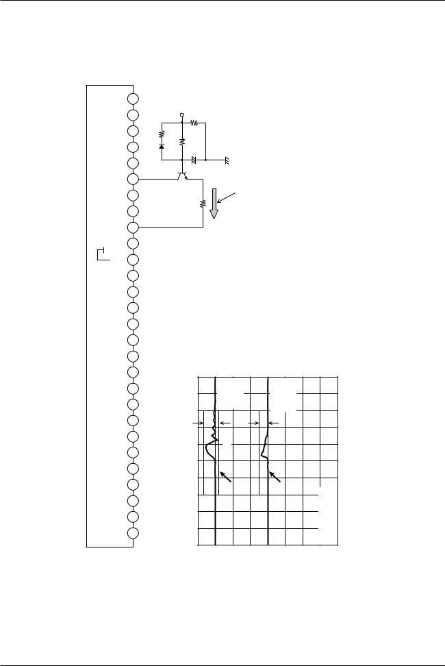
STK403-430
Standby Mode Control
|
Ch6 |
OUT |
28 |
|
|
Ch6 |
NF |
27 |
|
|
Ch6 |
IN |
26 |
3kΩ |
|
Ch5 |
IN |
25 |
|
|
Ch5 |
NF |
24 |
|
|
BIAS |
(ST-BY) |
23 |
|
|
Ch4 |
NF |
22 |
|
|
Ch4 |
IN |
21 |
|
|
|
+PRE |
20 |
|
SUB |
SUB |
GND GND |
18 19 |
|
|
|
PRE |
17 |
|
400 series |
Ch4 Ch5 |
CC OUT OUT -- |
15 16 |
|
STK403- |
|
CC |
13 14 |
|
|
|
+V |
|
|
|
|
CC |
|
|
|
|
--V |
|
|
|
|
--V |
12 |
|
|
|
CC |
11 |
|
|
|
+V |
|
|
|
Ch2 |
OUT |
10 |
|
|
Ch3 |
OUT |
9 |
|
|
Ch3 |
NF |
8 |
|
|
Ch3 |
IN |
7 |
|
|
Ch2 |
IN |
6 |
|
|
Ch2 |
NF |
5 |
|
|
Ch1 |
NF |
4 |
|
|
Ch1 |
IN |
3 |
|
|
|
+PRE |
2 |
|
|
Ch1 |
OUT |
1 |
|
Stand-by Control H : Operation Mode (+5 V) L : Stand-by Mode (0 V) |
ITF02250 |
|
Ω |
2kΩ |
|
|
|
|
33k |
/10V |
|
|
33F |
|
|
µ |
|
|
+ |
|
|
R1 |
|
|
Ω |
|
|
*(1) 6.2k |
I |
|
|
ST |
|
|
Current flowing in |
´2) / R1 |
|
BE |
|
=(applied voltage–V |
=(5--0.6´2) / 6.2kΩ ≈0.63(mA) |
ST |
|
I |
|
An internal transistor turns on when a voltage over 0.6 V is applied and the IC transitions to operating mode. |
23 IST ... Use a value for the limiting resistor that assures that the maximum operating current flowing into this pin due to the control voltage applied by the microcontroller or other circuit does not exceed the maximum rating. |
ST |
pin |
... |
|
• Applied voltage V |
• Current flowing into |
OFF (Stand-by |
Mode) |
ON |
(Operation |
Mode) |
ITF02263 |
0.16V |
|
0.1V |
|
|
|
|
|
|
|
V : 200mV / 1div |
T : 100ms / 1div |
•Impulse noise that occurs at power on and power off can be reduced significantly by using a standby circuit.
•End product design is made easier by using a limiting resistor *1 to match the control voltage provided by the microcontroller or other control circuit.
•Standby control can be applied by controlling the current (IST) flowing into the standby pin (pin 23).
No. 7374-7/8
STK403-430
|
2 |
|
|
|
|
|
|
THD — PO |
|
|
|
|
|
|
|
|||||||
|
|
VCC=±23V |
|
|
|
|
|
|
|
|
|
|
|
|
|
|
|
|
|
|||
% |
10 |
RL=6Ω |
|
|
|
|
|
|
|
|
|
|
|
|
|
|
|
|
|
|
|
|
|
|
|
|
|
|
|
|
|
|
|
|
|
|
|
|
|
|
|
||||
7 |
VG=30dB |
|
|
|
|
|
|
|
|
|
|
|
|
|
|
|
|
|
||||
— |
|
|
|
|
|
|
|
|
|
|
|
|
|
|
|
|
|
|||||
5 |
Rg=600Ω |
|
|
|
|
|
|
|
|
|
|
|
|
|
|
|
|
|
||||
|
|
|
|
|
|
|
|
|
|
|
|
|
|
|
|
|
||||||
THD |
3 |
Tc=25°C |
|
|
|
|
|
|
|
|
|
|
|
|
|
|
|
|
|
|||
|
|
|
|
|
|
|
|
|
|
|
|
|
|
|
|
|
|
|||||
distortion, |
2 |
6ch Drive |
|
|
|
|
|
|
|
|
|
|
|
|
|
|
|
|
|
|||
|
|
|
|
|
|
|
|
|
|
|
|
|
|
|
|
|
||||||
5 |
|
|
|
|
|
|
|
|
|
|
|
|
|
|
|
|
|
|
|
|
|
|
|
1.0 |
|
|
|
|
|
|
|
|
|
|
|
|
|
|
|
|
|
|
|
|
|
|
|
|
|
|
|
|
|
|
|
|
|
|
|
|
|
|
|
|
|
|
|
|
|
7 |
|
|
|
|
|
|
|
|
|
|
|
|
|
|
|
|
|
|
|
|
|
|
|
|
|
|
|
|
|
|
|
|
|
|
|
|
|
|
|
|
|
|
|
|
|
|
|
|
|
|
|
|
|
|
|
|
|
|
|
|
|
|
|
|
|
|
|
harmonic |
|
|
|
|
|
|
|
|
|
|
f=20kHz |
|
|
|
|
|
|
|
|
|
||
3 |
|
|
|
|
|
|
|
|
|
|
|
|
|
|
|
|
|
|
|
|
|
|
|
|
|
|
|
|
|
|
|
|
|
|
|
|
|
|
|
|
|
|
|
|
|
|
2 |
|
|
|
|
|
|
|
|
|
|
|
|
|
|
|
|
|
|
|
|
|
|
|
|
|
|
|
|
|
|
|
|
|
|
|
|
|
|
|
|
|
|
|
|
Total |
0.1 |
|
|
|
|
|
|
|
|
|
|
|
|
|
|
|
|
|
|
|
|
|
|
|
|
|
|
|
|
|
f=1kHz |
|
|
|
|
|
|
|
|
|
|||||
5 |
|
|
|
|
|
|
|
|
|
|
|
|
|
|
|
|
|
|||||
|
7 |
|
|
|
|
|
|
|
|
|
|
|
|
|
|
|
|
|
|
|
|
|
|
3 |
|
|
|
|
|
|
|
|
|
|
|
|
|
|
|
|
|
|
|
|
|
|
|
|
|
|
|
|
|
|
|
|
|
|
|
|
|
|
|
|
|
|
|
|
|
|
|
|
|
|
|
|
|
|
|
|
|
|
|
|
|
|
|
|
|
|
|
|
|
|
|
|
|
|
|
|
|
|
|
|
|
|
|
|
|
|
|
|
|
|
|
2 |
|
|
|
|
|
|
|
|
|
|
|
|
|
|
|
|
|
|
|
|
|
|
0.1 |
2 |
3 |
5 |
7 |
1.0 |
2 |
3 |
|
5 |
7 |
10 |
2 |
3 |
5 |
|||||||
|
|
|
|
|
|
|
Output power, PO — W |
|
|
|
ITF02251 |
|||||||||||
|
80 |
RL=6Ω |
|
PO — VCC |
|
|
|
||
|
70 |
f=1kHz |
|
|
|
|
|
|
|
|
|
VG=30dB |
|
|
|
|
|
|
|
W |
60 |
Rg=600Ω |
|
|
|
|
|
|
|
|
Tc=25°C |
|
|
|
|
|
|
|
|
— |
50 |
6ch Drive |
|
|
|
|
|
|
|
O |
|
|
|
|
|
|
|
|
|
P |
|
|
|
THD=10% |
|
|
.6% |
|
|
power, |
|
|
|
|
|
|
|||
40 |
|
|
.6% |
THD=0 |
|
||||
|
|
|
|
||||||
|
|
|
|
|
|||||
|
|
|
|
|
|
|
|||
|
30 |
|
|
|
|
|
|
||
Output |
|
|
|
THD=0 f=20kHz, |
|
|
|
||
|
|
|
|
|
|
|
|||
20 |
|
|
|
|
|
|
|
|
|
|
|
|
|
|
|
|
|
|
|
|
10 |
|
|
|
|
|
|
|
|
|
0 |
|
|
|
|
|
|
|
|
|
10 |
14 |
18 |
22 |
26 |
30 |
34 |
38 |
42 |
Supply voltage, ±VCC — V |
ITF02253 |
Total device power dissipation, Pd — W
Output power, PO — W
Pd — PO
120
VCC=±23V RL=6Ω
100 f=1kHz VG=30dB Rg=600Ω
80Tc=25°C 6ch Drive
60 (same output rating)
40 |
|
|
|
|
|
|
|
|
|
|
|
|
|
20 |
|
|
|
|
|
|
|
|
|
|
|
|
|
0 |
2 |
3 |
5 |
7 |
|
2 |
3 |
5 |
7 |
|
2 |
3 |
5 |
0.1 |
1.0 |
10 |
|||||||||||
|
|
|
|
Output power, PO — W |
|
|
ITF02252 |
||||||
PO — f
40
VCC=±23V, RL=6Ω
VG=30dB, Rg=600Ω Tc=25°C
35 6ch drive
THD=10%
30
25
THD=0.6%
20
15 |
|
|
|
|
|
|
|
|
|
|
|
|
|
|
|
|
|
10 |
2 |
3 |
5 |
7 100 |
2 |
3 |
5 |
7 |
1k |
2 |
3 |
5 |
7 10k |
2 |
3 |
||
|
|
|
|
|
Frequency, f — Hz |
|
|
|
ITF02254 |
||||||||
 Specifications of any and all SANYO products described or contained herein stipulate the performance, characteristics, and functions of the described products in the independent state, and are not guarantees of the performance, characteristics, and functions of the described products as mounted in the customer’s products or equipment. To verify symptoms and states that cannot be evaluated in an independent device, the customer should always evaluate and test devices mounted in the customer’s products or equipment.
 SANYO Electric Co., Ltd. strives to supply high-quality high-reliability products. However, any and all semiconductor products fail with some probability. It is possible that these probabilistic failures could give rise to accidents or events that could endanger human lives, that could give rise to smoke or fire, or that could cause damage to other property. When designing equipment, adopt safety measures so that these kinds of accidents or events cannot occur. Such measures include but are not limited to protective circuits and error prevention circuits for safe design, redundant design, and structural design.
 In the event that any or all SANYO products (including technical data, services) described or contained herein are controlled under any of applicable local export control laws and regulations, such products must not be exported without obtaining the export license from the authorities concerned in accordance with the above law.
 No part of this publication may be reproduced or transmitted in any form or by any means, electronic or mechanical, including photocopying and recording, or any information storage or retrieval system, or otherwise, without the prior written permission of SANYO Electric Co., Ltd.
 Any and all information described or contained herein are subject to change without notice due to product/technology improvement, etc. When designing equipment, refer to the “Delivery Specification” for the SANYO product that you intend to use.
 Information (including circuit diagrams and circuit parameters) herein is for example only; it is not guaranteed for volume production. SANYO believes information herein is accurate and reliable, but no guarantees are made or implied regarding its use or any infringements of intellectual property rights or other rights of third parties.
This catalog provides information as of December, 2003. Specifications and information herein are subject to change without notice.
PS No. 7374-8/8

Ordering number : ENN*7375
Thick-Film Hybrid IC
STK403-440
Six-Channel Class AB Audio Power Amplifier IC
25 W × 6 Channels
Preliminary
Overview
The STK403-400 series products are audio power amplifier hybrid ICs that consist of optimally-designed discrete component power amplifier circuits that have been miniaturized using SANYO’s unique insulated metal substrate technology (IMST). The adoption of a newlydeveloped low thermal resistance substrate allows this product to integrate six power amplifier channels in a single compact package. The adoption of a standby circuit in this device allows it to reduce impulse noise significantly as compared to earlier Sanyo products, in particular, the STK402-*00 series products.
Features
•Series of pin compatible power amplifiers ranging from 30 W/ch to 45 W/ch (10%/1 kHz) devices. The same printed circuit board can be used depending on the output power grade.
•Miniature packages
—78.0 mm × 32.0 mm × 9.0 mm *
*: Not including the pins.
•Output load impedance: RL = 6 Ω
•Allowable load shorted time: 0.3 seconds
•Supports the use of standby and muting circuits.
Package Dimensions
unit: mm
4202-SIP28
[STK403-440]
SANYO: SIP28
 Any and all SANYO products described or contained herein do not have specifications that can handle applications that require extremely high levels of reliability, such as life-support systems, aircraft’s control systems, or other applications whose failure can be reasonably expected to result in serious physical and/or material damage. Consult with your SANYO representative nearest you before using any SANYO products described or contained herein in such applications.
 SANYO assumes no responsibility for equipment failures that result from using products at values that exceed, even momentarily, rated values (such as maximum ratings, operating condition ranges, or other parameters) listed in products specifications of any and all SANYO products described or contained herein.
SANYO Electric Co.,Ltd. Semiconductor Company
TOKYO OFFICE Tokyo Bldg., 1-10, 1 Chome, Ueno, Taito-ku, TOKYO, 110-8534 JAPAN
21604TN (OT) No. 7375-1/8

STK403-440
Series Organization
These products are organized as a series based on their output capacity.
Item |
|
Type No. |
|
|
|
|
|
||
STK403-430 |
STK403-440 |
STK403-450 |
||
|
||||
|
|
|
|
|
Output 1 (10%/1 kHz) |
30 W × 6 ch |
40 W × 6 ch |
45 W × 6 ch |
|
Output 2 (0.6%/20 Hz to 20 kHz) |
20 W × 6 ch |
25 W × 6 ch |
30 W × 6 ch |
|
Maximum supply voltage (No signal) |
±36 V |
±38 V |
±40 V |
|
|
|
|
|
|
Maximum supply voltage (6 Ω ) |
±34 V |
±36 V |
±38 V |
|
Recommended supply voltage (6 Ω ) |
±23 V |
±26 V |
±28 V |
|
Package |
|
78.0 mm × 32.0 mm × 9.0 mm |
|
Specifications
Maximum Ratings at Ta = 25°C
Parameter |
|
Symbol |
|
|
|
Conditions |
|
|
Ratings |
|
Unit |
||||
|
|
|
|
|
|
|
|
|
|
|
|
|
|
|
|
Maximum supply voltage (No signal) |
|
VCC max(0) |
|
|
|
|
|
|
|
±38 |
|
V |
|||
Maximum supply voltage |
|
VCC max(1) |
RL ≥ 6 Ω |
|
|
|
|
|
±36 |
|
V |
||||
Minimum operating supply voltage |
|
VCC min |
|
|
|
|
|
|
|
±10 |
|
V |
|||
Maximum operation flow-in current (pin 23) |
IST OFF max |
|
|
|
|
|
|
|
1.2 |
|
mA |
||||
Thermal resistance |
|
θ j -c |
|
Per power transistor |
|
|
|
3.6 |
|
°C/W |
|||||
|
|
|
|
|
|
|
|
|
|
|
|
|
|
|
|
Junction temperature |
|
Tj max |
Both the Tj max and the Tc max conditions must be met. |
|
|
150 |
|
°C |
|||||||
|
|
|
|
|
|
|
|
|
|
|
|||||
Operating IC substrate temperature |
|
Tc max |
|
|
125 |
|
°C |
||||||||
|
|
|
|
|
|
|
|
|
|||||||
|
|
|
|
|
|
|
|
|
|
|
|
|
|
|
|
Storage temperature |
|
Tstg |
|
|
|
|
|
|
|
–30 to +125 |
|
°C |
|||
|
|
|
|
|
|
|
|
|
|
|
|
|
|
|
|
Allowable load shorted time *4 |
|
ts |
|
VCC = ±26.0 V, RL = 6 Ω , f = 50 Hz, PO = 25 W, 1ch drive |
|
|
0.3 |
|
s |
||||||
Operating Characteristics at Tc = 25°C, RL = 6 Ω (noninductive load), Rg = 600 Ω , VG = 30 dB |
|
|
|
||||||||||||
|
|
|
|
|
|
|
|
|
|
|
|
|
|
|
|
Parameter |
|
Symbol |
|
|
|
|
Conditions*1 |
|
|
Ratings |
|
|
Unit |
||
|
|
|
|
|
VCC (V) |
f (Hz) |
PO (W) |
THD (%) |
|
min |
typ |
max |
|
|
|
Output power *1 |
|
PO (1) |
|
±26.0 |
20 to 20 k |
|
0.6 |
|
23 |
25 |
|
|
W |
||
|
PO (2) |
|
±26.0 |
1 k |
|
10 |
|
|
40 |
|
|
||||
|
|
|
|
|
|
|
|
|
|||||||
Total harmonic distortion *1 |
|
THD (1) |
|
±26.0 |
20 to 20 k |
5.0 |
|
VG = 30 dB |
|
|
0.6 |
|
% |
||
|
|
|
|
|
|
|
|
|
|
|
|
|
|
||
|
THD (2) |
|
±26.0 |
1 k |
5.0 |
|
VG = 30 dB |
|
0.03 |
|
|
||||
|
|
|
|
|
|
|
|
||||||||
|
|
|
|
|
|
|
|
|
|
|
|
|
|
||
Frequency characteristics |
|
fL, fH |
|
±26.0 |
|
1.0 |
|
+0 –3 dB |
|
20 to 50 k |
|
|
Hz |
||
Input impedance |
|
ri |
|
±26.0 |
1 k |
1.0 |
|
|
|
55 |
|
|
kΩ |
||
|
|
|
|
|
|
|
|
|
|
|
|
|
|
||
Output noise voltage *2 |
|
VNO |
|
±31.0 |
|
|
|
Rg = 2.2 kΩ |
|
|
1.0 |
|
mVrms |
||
Quiescent current |
|
ICCO |
|
±31.0 |
|
|
|
No loading |
60 |
110 |
180 |
|
mA |
||
Neutral voltage |
|
VN |
|
±31.0 |
|
|
|
|
–70 |
0 |
+70 |
|
mV |
||
Current flowing into pin 23 |
|
IST ON |
|
±26.0 |
|
|
|
V23 = 5 V, current limiting |
|
|
0 |
|
mA |
||
in standby mode *6 |
|
|
|
|
|
resistance: 6.2 kΩ |
|
|
|
||||||
|
|
|
|
|
|
|
|
|
|
|
|
|
|
||
Current flowing into pin 23 |
|
IST OFF |
|
±26.0 |
|
|
|
|
0.4 |
|
1.2 |
|
mA |
||
in operating mode *6 |
|
|
|
|
|
|
|
|
|||||||
Notes: 1. 1ch drive
2.Unless otherwise noted, use a constant-voltage supply for the power supply used during inspection.
3.The output noise voltage values shown are peak values read with a VTVM. However, an AC stabilized (50 Hz) power supply should be used to minimize the influence of AC primary side flicker noise on the reading.
4.Use the transformer power supply circuit shown in the figure below for allowable load shorted time measurement and output noise voltage measurement.
5.Design applications so that the minus pre-VCC line (pin 17) is at the lowest potential at all times.
6.A limiting resistor that assures that the maximum operating current flowing into the standby pin (pin 23) does not exceed the maximum rating must be included in application circuits. This IC operates when a voltage higher than VBE (about 0.6 V) is applied to the standby pin.
DBA30C |
4700 µF |
 +VCC
+VCC
+
500 Ω
+  500 Ω
500 Ω
--VCC
4700 µF
Designated Transformer Power Supply (RP-25 equivalent)
No. 7375-2/8

TRTR
3/8-7375 .No
|
|
|
|
|
|
|
|
|
|
|
|
|
Internal |
|
|
|
|
|
|
5 |
6 |
7 |
8 |
|
|
|
Equivalent |
11 |
|
|
|
|
|
|
|
|
|
|
|
|
|
2 |
|
|
C11 |
C12 |
|
|
|
|
|
|
C13 |
|
|
|
|
|
|
|
|
|
|
|
|
|
|
||
|
|
|
TR1 |
|
|
|
|
|
|
|
TR7 |
|
|
|
|
|
|
|
|
|
|
|
|
|
Circuit |
||
3 |
|
R1 |
R20 |
|
R22 |
R3 |
|
|
R5 |
R24 |
|
|
|
|
Pre driver IC |
|
Pre driver IC |
|
|
|
|||||||
4 |
|
TR3 |
|
TR6 |
|
|
TR9 |
|
9 |
|
|||
(CH1) |
R2 |
|
R4 |
(CH2 / CH3) |
R6 |
|
|
||||||
|
R21 |
|
R23 |
R25 |
|
|
|
||||||
|
|
|
|
|
|
|
|
||||||
|
|
|
|
|
|
|
|
|
|
|
|||
|
|
|
TR2 |
|
|
|
|
|
|
|
TR8 |
|
|
|
|
C1 |
|
4 |
|
C2 |
|
|
C3 |
|
|
|
|
|
|
|
1 |
|
|
|
|
|
|
|
|||
1 |
|
|
|
13 |
|
|
|
|
|
|
|
|
|
|
|
|
R |
|
|
|
|
|
|
|
|
|
|
10 |
|
|
|
|
Bias circuit |
|
|
|
|
|
23 |
-STK403 |
|
12 |
|
|
|
|
|
|
|
|
|
|
19 |
||
13 |
|
|
|
|
|
|
|
|
|
|
|||
|
|
|
|
|
|
|
|
|
|
|
|||
|
|
|
|
|
|
|
|
|
|
|
|
||
16 |
|
|
|
|
|
|
|
|
|
|
18 |
440 |
|
15 |
|
|
|
|
|
|
|
|
|
SUB |
|
||
|
C4 |
|
|
C5 |
|
|
C6 |
|
|
|
|||
|
|
|
|
|
|
|
|
|
|
||||
|
|
|
TR11 |
|
|
|
|
|
|
TR17 |
|
|
|
|
|
|
T |
|
|
|
|
|
|
|
|
||
20 |
|
|
|
R |
|
|
|
|
|
|
|
|
|
21 |
|
|
R27 |
|
|
|
|
|
|
|
|
|
|
22 |
Pre driver IC |
R8 |
R29 |
R10 |
Pre driver IC |
R12 |
R31 |
|
28 |
|
|||
|
TR12 |
TR15 |
|
|
TR18 |
|
|
||||||
(CH4) |
|
|
(CH5 / CH6) |
|
|
|
|||||||
|
R7 |
|
|
R9 |
R11 |
|
|
|
|
||||
|
|
R26 |
R28 |
|
|
R30 |
|
|
|
||||
17 |
|
|
|
|
|
|
|
|
|
|
|
|
|
|
|
|
TR10 |
|
|
|
|
|
|
TR16 |
|
|
|
|
|
|
T |
|
|
|
|
|
|
|
|
||
|
|
|
C14 |
C15 |
|
|
|
|
|
|
C16 |
|
|
14 |
|
|
|
|
|
|
|
|
|
|
|
|
|
|
|
|
|
|
|
24 |
25 |
26 |
27 |
|
ITF02247 |
|
|
|
|
|
|
|
|
|
|
|
|
|
|
|
|
45
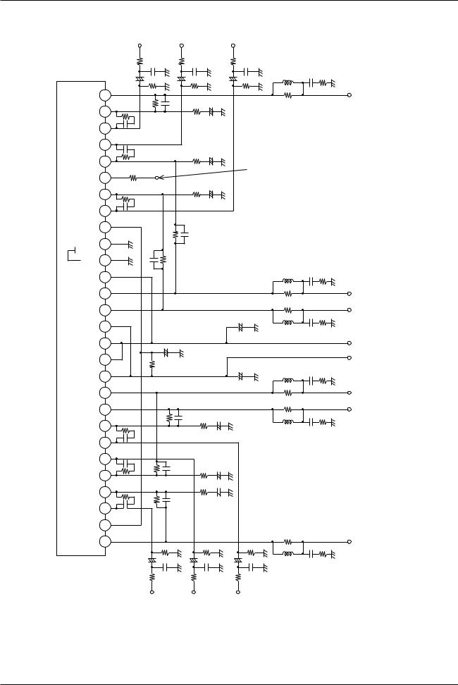
STK403-440
Sample Application Circuit
|
|
|
|
|
µF2.21 kΩ |
|
Ch6 |
IN |
|
µF2.21 kΩ |
|
Ch5 IN |
|
|
µF2.21 kΩ |
|
|
Ch4 |
IN |
|
|
|
|
|
|
|
|
ITF02248 |
rating. |
|||
|
|
|
|
|
+ |
|
|
|
+ |
|
|
|
|
|
+ |
470pF |
|
|
|
|
|
|
|
|
||||||||
|
|
|
|
|
|
470 pF |
|
|
470 pF |
|
|
|
|
|
|
|
|
|
|
|
|
|
|
|
||||||||
|
|
|
|
|
|
|
|
|
|
|
|
|
|
|
|
|
|
|
|
|
|
|
|
F |
|
3 |
|
Ω |
7.4 |
|
|
|
|
|
|
|
|
|
|
56kΩ |
|
|
|
56kΩ |
|
|
|
|
|
|
56kΩ |
|
µ |
|
|
|
|
|
|
||||||
|
|
|
|
|
|
|
|
|
|
|
|
|
|
|
|
|
|
7.4 |
|
|
|
|
|
maximum |
||||||||
|
Ch6Ch6 |
OUTNF |
2827 |
|
|
Ωk56 |
|
|
pF3 |
|
|
|
+ |
|
|
|
|
|
|
|
Ω |
F |
1.0 |
|
Ch6 |
OUT |
||||||
|
|
|
|
|
|
|
|
|
|
|
|
|
|
|
|
|
|
µ |
|
|
||||||||||||
|
|
|
|
|
|
|
|
|
|
|
|
|
|
|
|
|
|
|
|
|
|
|
|
|
|
|
|
|
|
|
|
|
|
|
|
|
|
|
|
|
|
|
|
|
Ω |
8.1k |
F |
10 |
|
|
|
|
|
|
|
|
|
|
|
|
|
|
|
||
|
|
|
|
3kΩ |
|
|
|
|
|
|
|
|
|
µ |
|
|
|
|
|
|
|
|
|
|
|
|
|
|
|
|
||
|
|
|
|
|
|
|
|
|
|
|
|
|
|
|
|
|
|
|
|
|
|
|
|
|
|
|
|
|
|
|
||
|
Ch6 |
IN |
26 |
220pF |
|
|
|
|
|
|
|
|
|
|
|
|
|
|
|
|
|
|
|
|
|
|
|
|
|
|
the |
|
|
Ch5BIASCh5 |
NFBY)-(ST IN |
2423 25 |
|
|
|
|
|
|
|
8.1k |
F |
10 |
|
|
|
|
by-Stand |
control |
|
|
|
|
|
|
|
|
exceednotdoes |
||||
|
* |
|
|
|
|
|
|
|
|
|
|
|
|
|
|
|
|
|
|
|
|
|||||||||||
|
|
|
|
220 pF |
|
|
|
|
|
|
|
|
|
|
|
|
|
|
|
|
|
|
|
|
|
|
|
|
|
|
|
|
|
|
|
|
|
|
|
|
|
|
|
|
Ω |
8.1 k |
F |
10 |
|
|
|
|
|
|
|
|
|
|
|
|
|
|
|
||
|
|
|
|
|
|
|
|
|
|
|
|
|
|
|
µ |
|
|
|
|
|
|
|
|
|
|
|
|
|
|
|
|
|
|
|
|
|
3kΩ |
|
|
|
|
|
|
|
|
+ |
|
|
|
|
|
|
|
|
|
|
|
|
|
|
|
|
|||
|
|
|
|
|
|
|
|
|
|
|
|
|
|
|
|
|
|
|
|
|
|
|
|
|
|
|
|
|
|
|
||
|
|
|
|
|
2.6kΩ |
|
|
|
|
|
|
|
|
|
|
|
|
|
|
|
|
|
|
|
|
|
|
|
|
|
|
|
|
Ch4 |
NF |
22 |
3kΩ |
|
|
|
|
|
|
Ω |
|
|
|
µ |
|
|
|
|
|
|
|
|
|
|
|
|
|
|
|
23) |
|
|
|
|
|
|
|
|
|
|
+ |
|
|
|
|
|
|
|
|
|
|
|
|
|
|
|
||||||||
|
|
|
|
|
|
|
|
|
|
|
|
|
|
|
|
|
|
|
|
|
|
|
|
|
|
|||||||
|
Ch4 |
IN |
21 |
220pF |
|
|
|
|
|
|
|
|
|
|
|
|
|
|
|
|
|
|
|
|
|
|
|
|
|
|
(pin |
|
|
|
GND GND +PRE |
|
|
|
|
|
|
|
|
|
|
|
|
|
|
|
|
|
|
|
|
|
|
|
|
|
|
|
the standby pin |
||
|
SUB SUB |
18 19 20 |
|
|
3 pF |
|
|
56 kΩ 56 kΩ |
|
3 pF |
|
|
|
|
|
|
|
|
|
|
|
|
|
|
|
|
|
|
||||
series400-STK403 |
Ch5Ch4Ch2 |
--PRE |
1716151413121110 |
|
|
Ω100 |
|
|
|
|
|
|
|
|
|
|
|
+ |
|
|
|
F |
|
3 |
|
Ω |
7.4 |
+VCh2 |
OUTOUTOUT |
intoflowingcurrentoperatingmaximum |
||
OUT |
|
|
|
|
|
|
|
|
|
|
|
|
|
|
|
|
|
|
||||||||||||||
|
|
|
|
|
|
|
|
|
|
|
|
|
|
|
|
|
|
|
|
|
|
|
|
µ |
|
|
|
|
|
|
||
|
|
OUT |
|
|
|
|
|
|
|
|
|
|
|
|
|
|
|
|
|
|
|
|
|
Ω |
7.4 |
F |
1.0 |
|
Ch5 |
|
|
|
|
|
|
|
|
|
|
|
|
|
|
|
|
|
|
|
|
|
|
|
|
|
|
|
|
|
µ |
|
|
|
|
||
|
|
|
|
|
|
|
|
|
|
|
|
|
|
|
|
|
|
|
|
|
|
|
|
|
|
|
|
|
|
|
||
|
|
OUT |
|
|
|
|
|
|
|
|
|
|
|
|
|
|
|
|
F |
|
470 |
|
Ω |
7.4 |
|
Ω |
7.4 |
Ch4 |
|
|
||
|
|
|
|
|
|
|
|
|
|
|
|
|
|
|
|
|
|
|
|
|
|
|
|
|
||||||||
|
|
CC |
|
|
|
|
|
|
|
|
|
|
|
|
|
|
|
|
µ |
|
|
|
|
|
|
|
|
|
|
|
|
|
|
|
|
|
|
|
|
|
|
|
|
|
|
|
|
|
|
|
|
|
|
|
|
µ |
|
F |
1.0 |
|
|
|
|
||
|
|
+V |
|
|
|
|
|
|
|
|
|
|
|
|
|
|
|
|
|
|
|
|
|
3 |
|
|
|
|
||||
|
|
|
|
|
|
|
|
|
|
|
|
|
|
|
|
|
|
|
|
|
+ |
|
|
F |
|
µ |
|
|
CC |
|
|
|
|
|
CC |
|
|
|
|
|
|
|
|
|
|
|
|
|
|
|
|
|
|
|
|
|
|
|
|
|
|
|
|||
|
|
|
|
|
|
|
|
|
|
|
|
|
|
|
|
|
|
|
|
|
|
|
|
|
|
|
|
|
|
|||
|
|
--V |
|
|
|
|
|
+ |
|
|
|
|
|
|
|
|
|
|
|
|
|
|
|
|
|
|
|
|
V-- |
|
|
|
|
|
V-- |
|
|
|
|
|
µ |
|
|
|
|
|
|
|
|
|
|
|
|
|
|
|
|
|
|
|
|
CC |
|
|
|
|
|
CC |
|
|
|
|
|
F |
|
100 |
|
|
|
|
|
|
|
|
|
|
|
|
|
|
|
|
|
|
|
|
|
|
|
|
|
|
|
|
|
|
|
|
|
|
|
|
|
|
|
F |
|
470 |
|
|
|
|
|
|
|
|
|
|
|||
|
|
|
|
|
|
|
|
|
|
|
|
|
|
|
|
|
|
|
|
|
|
|
|
|
|
|
|
|
|
|||
|
|
CC |
|
|
|
|
|
|
|
|
|
|
|
|
|
|
|
|
µ |
|
|
|
F |
|
3 |
|
Ω |
7.4 |
|
|
|
|
|
|
+V |
|
|
|
|
|
|
|
|
|
|
|
|
|
|
|
|
|
|
|
|
|
µ |
|
|
|
|
|
|
||
|
|
|
|
|
|
|
|
|
|
|
|
|
|
|
|
|
|
|
|
|
|
|
Ω |
7.4 |
|
|
|
|
|
|
||
|
|
|
|
|
|
|
|
|
|
|
|
|
|
|
|
|
|
|
|
|
|
|
|
F |
1.0 |
|
|
|
|
|||
|
Ch3Ch3 |
NFOUT |
|
|
|
|
|
|
|
|
|
|
|
|
|
|
|
|
|
|
|
|
|
|
|
|
µ |
|
|
|
|
thatthe |
|
8 9 |
|
|
|
|
56kΩ |
3 pF |
|
|
|
|
+ |
|
|
|
|
|
|
Ω |
7.4 |
|
|
7.4 |
Ch3 |
OUT |
|||||||
|
|
|
|
|
|
|
|
|
|
|
|
|
Ω |
8.1 k |
F |
10 |
|
|
|
|
|
|
Ω |
|
|
|
||||||
|
|
|
|
3kΩ |
|
|
|
|
|
|
|
|
|
|
µ |
|
|
|
|
|
|
|
|
|
|
|
|
|
|
|||
|
|
|
|
|
|
|
|
|
|
|
|
|
|
|
|
|
|
|
|
|
|
F |
|
3 |
µF |
1.0 |
|
|
|
|
||
|
Ch2Ch2Ch1Ch3 |
INNFNFIN |
654 7 |
|
|
|
ΩΩk56k |
|
|
pF3pF |
|
|
|
|
|
|
|
|
|
|
|
|
|
µ |
|
|
|
|
assuresthatresistor |
|||
|
220pF |
|
|
|
|
|
|
|
|
+ |
|
|
|
|
|
|
|
|
|
|
|
|
|
|
||||||||
|
|
|
|
|
|
|
|
|
|
|
|
|
|
|
|
|
|
|
|
|
|
|
|
|
|
|
|
|
|
|
||
|
|
|
|
220pF |
|
|
|
|
|
|
|
|
|
|
|
|
|
|
|
|
|
|
|
|
|
|
|
|
|
|
|
|
|
|
|
|
|
|
|
|
|
|
|
|
|
Ω |
8.1k |
F |
10 |
|
|
|
|
|
|
|
|
|
|
|
|
|
|
||
|
|
|
|
|
|
|
|
|
|
|
|
|
|
|
|
µ |
|
|
|
|
|
|
|
|
|
|
|
|
|
|
|
|
|
|
|
|
3kΩ |
|
|
|
|
|
|
|
|
|
|
+ |
|
|
|
|
|
|
|
|
|
|
|
|
|
|
|
||
|
|
|
|
|
|
|
|
|
|
|
Ω |
8.1k |
F |
10 |
|
|
|
|
|
|
|
|
|
|
|
|
|
|
||||
|
|
|
|
3kΩ |
|
|
|
|
|
|
|
|
|
|
µ |
|
|
|
|
|
|
|
|
|
|
|
|
|
|
|
||
|
Ch1 Ch1 |
OUT+PRE IN |
21 3 |
|
|
|
|
|
|
|
|
|
|
|
|
|
|
|
|
|
|
|
|
|
|
|
|
Ch1 |
OUT |
theforlimiting |
||
|
|
|
|
56 |
|
56k |
|
|
|
|
56k |
|
|
|
|
|
56k |
|
|
|
|
|
|
|||||||||
|
|
|
|
|
|
|
|
|
|
3 |
|
|
|
|
|
|
|
|
|
|
|
|
|
|
|
|
|
|
|
|
|
|
|
|
|
|
220pF |
|
|
|
|
|
|
|
|
|
|
|
|
|
|
|
|
|
|
|
|
|
|
|
|
|
|
|
|
|
|
|
|
|
|
2.2µF |
|
Ω |
|
|
2.2µF |
|
|
Ω |
|
|
|
2.2µF |
|
|
Ω |
|
|
Ω |
7.4 |
|
Ω |
7.4 |
|
|
value |
|
|
|
|
|
|
|
+ |
|
|
|
|
+ |
|
|
|
|
|
+ |
|
|
F |
|
3 |
µ |
|
|
|
|
|||||
|
|
|
|
|
|
|
|
|
|
|
|
|
|
|
|
|
|
|
|
|
|
|
|
µ |
|
F |
1.0 |
|
|
|
|
|
|
|
|
|
|
|
Ω |
|
470pF |
Ω |
|
470pF |
|
Ω |
|
|
470pF |
|
|
|
|
|
|
|
|
a |
|||||||
|
|
|
|
|
|
1 k |
|
1 k |
|
|
1 k |
|
|
|
|
|
|
|
|
|
|
Use |
||||||||||
|
|
|
|
|
|
|
Ch1 |
|
|
|
Ch2 |
|
|
|
|
Ch3 IN |
|
|
|
|
|
|
|
|
|
|||||||
|
|
|
|
|
|
|
|
IN |
|
|
|
IN |
|
|
|
|
|
|
|
|
|
|
|
|
|
*: |
||||||
No. 7375-4/8

STK403-440
Thermal Design Example
The heat sink thermal resistance, θc-a, required to handle the total power dissipated within this hybrid IC is determined as follows.
Condition 1: The IC substrate temperature Tc must not exceed 125°C.
Pd × θc-a + Ta < 125°C ... (1)
Ta: Guaranteed ambient temperature for the end product.
Condition 2: The junction temperature of each transistor must not exceed 150°C.
Pd × θc-a + Pd/N × θj-c + Ta < 150°C ... (2)
N: Number of power transistors
θj-c: Thermal resistance per power transistor
We take the power dissipation in the power transistors to be Pd evenly distributed across those N power transistors. If we solve for θc-a in equations (1) and (2), we get the following inequalities.
θc-a < (125 – Ta)/Pd ... (1)’
θc-a < (150 – Ta)/Pd –θj-c/N ... (2)’
Values that satisfy both these inequalities at the same time are the required heat sink thermal resistance values.
Determining the following specifications allows us to obtain the required heat sink thermal resistance from inequalities (1)’ and (2)’.
•Supply voltage: VCC
•Load resistance: RL
•Guaranteed ambient temperature: Ta
Example:
Assume that the IC supply voltage, VCC, is ±26 V, RL is 6 Ω , and that the signal is a continuous sine wave. In this case,
from the Pd – P characteristics, the maximum power will be 134 W for a signal with a frequency of 1 kHz.
O
For actual music signals, it is usual to use a Pd of 1/8 of POmax, which is the power estimated for continuous signals in this manner. (Note that depending on the particular safety standard used, a value somewhat different from the value of 1/8 used here may be used.)
That is:
Pd = 85 W (when 1/8 POmax is 3.1 W)
The number, N, of power transistors in the hybrid IC's audio amplifier block is 12. Since the thermal resistance, θj-c, per transistor is 3.6°C/W, the required heat sink thermal resistance, θc-a, for a guaranteed ambient temperature of 50°C will be as follows.
From inequality (1)’: θc-a < (125 – 50)/85
< 0.88
From inequality (2)’: θc-a < (150 – 50)/85 – 3.6/12
< 0.87
Therefore, the thermal resistance that satisfies both these expressions at the same time is 0.87°C/W.
Note that this thermal design example assumes the use of a constant-voltage power supply, and is only provided as an example for reference purposes. Thermal designs must be tested in an actual end product.
No. 7375-5/8
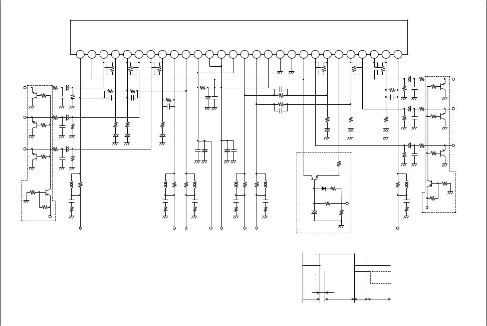
6/8-7375 .No
|
|
|
|
|
|
|
|
|
STK403-400 series |
|
|
|
|
|
|
|
|
|
|
|
|
|
|
|
|
|
|
|
|
|
|
|
|
SUB |
|
|
|
|
|
|
|
|
|||||
Ch1 |
Ch1 |
Ch1 |
Ch2 |
Ch2 |
Ch3 |
Ch3 |
Ch3 |
Ch2 |
Ch4 |
Ch5 |
SUB |
Ch4 |
Ch4 |
BIAS |
Ch5 |
Ch5 |
Ch6 |
Ch6 |
Ch6 |
||||
OUT +PRE |
IN |
NF |
NF |
IN |
IN |
NF |
OUT |
OUT |
+VCC --VCC --VCC +VCC OUT |
OUT --PRE |
GND GND +PRE |
IN |
NF |
(ST-BY) |
NF |
IN |
IN |
NF |
OUT |
||||
|
|
1 |
2 |
3 |
4 |
5 |
6 |
7 |
8 |
9 |
10 |
11 |
12 |
13 |
14 |
15 |
16 |
17 |
18 |
19 |
20 |
21 |
22 |
23 |
24 |
25 |
26 |
27 |
28 |
|
|
|
|
|
|
|
|
|
|
|
|
|
|
|
|
|
|
|
|
|
|
|
|
|
|
|
|
|
+ |
Ch1 |
+ |
|
|
|
|
|
|
|
|
|
|
+ |
|
|
|
|
|
|
|
|
|
|
|
|
|
|
|
|
|
|
|
|
|
|
|
|
|
|
|
|
|
|
|
|
|
|
|
|
|
|
|
|
|
|
|
|
|||
IN |
10 kΩ |
|
|
|
|
|
|
|
|
|
|
|
|
|
|
|
|
|
|
|
|
|
|
|
|
|
|
|
|
|
|
|
|
|
|
|
|
|
|
|
|
|
|
|
|
|
|
|
|
|
|
|
|
|
|
|
|
|
+ |
Ch2 |
+ |
|
|
|
|
|
|
|
|
|
|
|
|
|
|
|
|
|
|
|
|
|
|
|
|
|
|
|
|
|
|
|
|
|
|
|
|
|
|
|
|
|
|
|
|
|
|
|
|
|
+ |
|
+ |
|
|
+ |
|
||
IN |
10 kΩ |
|
|
|
|
|
|
|
|
|
|
|
|
|
|
|
|
|
|
|
|
|
|
|
|
|
|||
|
|
|
+ |
+ |
|
|
+ |
|
|
|
|
|
|
|
|
|
|
|
|
|
|
|
|
|
|
|
|
||
|
|
|
|
|
|
|
|
|
|
|
|
|
|
|
|
|
|
|
|
|
|
|
|
|
|
|
|||
|
|
+ |
|
|
|
|
|
|
|
|
|
|
+ |
|
|
|
|
|
|
|
|
|
|
|
|
|
|
|
+ |
Ch3 |
|
|
|
|
|
|
|
|
|
|
|
+ |
|
|
|
|
|
|
|
|
|
|
|
|
|
|
|
||
|
|
|
|
|
|
|
|
|
|
|
|
|
|
|
|
|
|
|
|
* |
|
|
|
|
|
||||
IN |
10 kΩ |
|
|
|
|
|
|
|
|
|
|
|
|
|
|
|
|
|
|
|
|
|
|
|
|
|
|
||
|
|
|
|
|
|
|
|
|
|
|
|
|
|
|
|
|
|
|
|
|
Ω |
|
|
|
|
|
|||
|
|
|
|
|
|
|
|
|
|
|
|
|
|
|
|
|
|
|
|
|
|
k |
|
|
|
|
|
||
|
|
|
|
|
|
|
|
|
|
|
|
|
|
|
|
|
|
|
|
|
|
|
6.2 |
|
|
|
|
|
|
|
10 kΩ |
|
|
|
|
|
|
|
|
|
|
|
|
|
|
|
|
|
|
|
|
|
3 kΩ |
|
|
|
|
|
|
|
|
|
|
|
|
|
|
|
|
|
|
|
|
|
|
|
|
|
|
|
|
|
|
|
|
|
|
|
|
|
|
|
|
|
|
|
|
|
|
|
|
|
|
|
|
|
|
|
|
|
|
|
33 kΩ |
|
Stand-by |
|
|
|
|
|
|
|
|
|
|
|
|
|
|
|
|
|
|
|
|
|
|
|
|
|
|
|
|
control |
|
|
|
||
|
2.2 kΩ |
|
|
|
|
|
|
|
|
|
|
|
|
|
|
|
|
|
|
|
33 µF |
+ |
|
|
H : Operation |
|
|
||
|
|
|
|
|
|
|
|
|
|
|
|
|
|
|
|
|
|
|
|
|
2 kΩ |
L : Stand-by |
|
|
|||||
|
|
|
|
|
|
|
|
|
|
|
|
|
|
|
|
|
|
|
|
|
|
|
|
||||||
|
|
|
|
|
|
|
|
|
|
|
|
|
|
|
|
|
|
|
|
|
|
|
|
|
|
|
|
||
|
Mute control |
Ch1 |
|
|
|
|
|
|
|
Ch3 |
Ch2 |
|
+VCC |
--VCC |
|
Ch4 |
Ch5 |
|
|
|
|
|
|
|
|
|
|
|
Ch6 |
|
H : Single mute |
|
|
|
|
|
|
|
|
|
|
|
|
|
|
|
|
|
|
|
|
||||||||
|
L : Normal |
OUT |
|
|
|
|
|
|
|
OUT OUT |
|
|
|
|
OUT OUT |
|
|
|
|
|
|
|
|
|
|
|
OUT |
||
|
|
|
|
|
|
|
|
|
|
|
|
|
|
|
|
|
|
|
|
|
|
|
|
|
|
|
|
|
|
*: Use a value for the limiting resistor that assures that the maximum operating current flowing into the standby pin (pin 23) does not exceed the maximum rating.
Stand-by +5 control


 +5 Mute
control 


 Mute
Mute
ST-BY |
Play |
Mute ST-BY |
|
Ch6 |
10 kΩ |
IN |
|
Ch5 |
10 kΩ |
IN |
|
Ch4 |
10 kΩ |
IN |
10 kΩ |
|
2.2 kΩ |
|
Mute control
H : Single mute L : Normal
ITF02249
440-STK403
Circuit Application Sample Mute & by-Stand
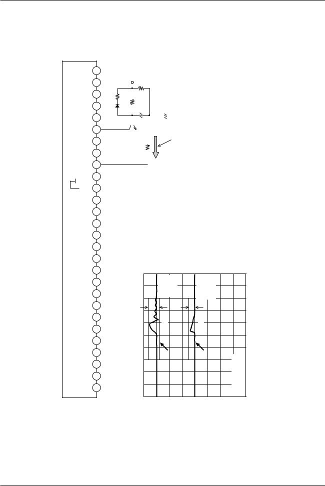
STK403-440
Standby Mode Control
|
Ch6 |
OUT |
28 |
|
|
Ch6 |
NF |
27 |
|
|
Ch6 |
IN |
26 |
kΩ |
|
Ch5 |
IN |
|
3 |
|
25 |
|
||
|
Ch5 |
NF |
24 |
|
|
BIAS |
(ST-BY) |
23 |
|
|
Ch4 |
NF |
22 |
|
|
Ch4 |
IN |
21 |
|
|
|
+PRE |
20 |
|
SUB |
SUB |
GND GND |
18 19 |
|
|
|
PRE |
17 |
|
400 series |
Ch4 Ch5 |
CC OUT OUT -- |
15 16 |
|
STK403- |
|
CC |
13 14 |
|
|
|
+V |
|
|
|
|
CC |
|
|
|
|
--V |
|
|
|
|
--V |
12 |
|
|
|
CC |
11 |
|
|
|
+V |
|
|
|
Ch2 |
OUT |
10 |
|
|
Ch3 |
OUT |
9 |
|
|
Ch3 |
NF |
8 |
|
|
Ch3 |
IN |
7 |
|
|
Ch2 |
IN |
6 |
|
|
Ch2 |
NF |
5 |
|
|
Ch1 |
NF |
4 |
|
|
Ch1 |
IN |
3 |
|
|
|
+PRE |
2 |
|
|
Ch1 |
OUT |
1 |
|
33 kΩ Stand-by control R1 H : Operation mode (+5 V) + |
k6.2*Ω |
|
|
|
IinflowingCurrent |
I |
0.6--(5= ≈0.63(mA) |
..................whenonturnstransistorinternalAn a voltage over 0.6 V is applied operatingintoentersICtheandmode. |
(I23 thisintoflowingcurrentoperatingpin due to the control voltage applied |
circuitotherormicrocontrollertheby does not exceed the maximum rating. |
||||||
|
|
|
|
V) (0 mode by - Stand |
|
|
|
|
|
|
ITF02250 |
R1 / 2) |
|
|
maximum the |
|
|
|
|
|
: L |
|
|
|
|
|
|
|
BE |
|
that |
|
|
|
|
|
|
|
|
|
|
|
|
|
|
× |
|
|
|
|
|
|
|
|
2 k Ω |
V – voltage Ω k 6.2 / 2) |
|
assures that |
|
||||||||
|
|
10 V |
/ |
|
|
|
|
|
|
|
|
|||||
|
|
F |
|
33 |
|
|
|
|
|
|
|
|
||||
|
|
µ |
|
|
|
|
|
|
(applied |
× |
|
resistor |
|
|||
|
|
|
|
|
|
|
|
|
|
|
|
|
|
|
||
|
|
|
|
|
|
|
|
|
|
|
|
|
|
|
||
|
|
|
|
|
|
|
|
|
|
|
|
ST |
|
limiting |
|
|
|
|
|
|
|
|
|
|
|
|
|
ST |
= |
|
|
for the |
|
|
|
|
|
|
|
|
|
|
|
|
|
|
|
|
||
|
|
|
|
|
|
|
|
|
|
|
|
|
|
|
||
|
|
|
|
|
|
|
|
|
|
|
|
|
||||
|
|
|
|
|
|
|
|
|
|
|
|
|
|
|
) ... Use a value |
|
|
|
|
|
|
|
|
|
|
|
|
|
|
|
|
|
|
|
|
|
|
|
|
|
|
|
|
|
|
|
|
|
ST |
|
|
|
|
|
|
|
|
|
|
|
|
|
|
|
ST |
pin |
|
|
|
|
|
|
|
|
|
|
|
|
|
|
|
) |
|
|
|
|
|
|
|
|
|
|
|
|
|
|
|
|
Applied voltage (V |
Current flowing into |
|
|
|
|
• |
• |
|
OFF (Stand-by |
mode) |
ON |
(Operation mode) |
|
ITF02263 |
0.16 V |
|
0.1 V |
|
|
|
|
|
|
|
V : 200 mV / 1div |
T : 100 ms / 1div |
•Impulse noise that occurs at power on and power off can be reduced significantly by using a standby circuit.
•End product design is made easier by using a limiting resistor (*) to match the control voltage provided by the microcontroller or other control circuit.
•Standby control is available by controlling the current (IST) flowing into the standby pin (pin 23).
No. 7375-7/8
STK403-440
|
2 |
|
|
|
|
|
|
|
THD — PO |
|
|
|
|
|
|
|
|
|
||||||
|
|
VCC = ±26 V |
|
|
|
|
|
|
|
|
|
|
|
|
|
|
|
|
|
|
||||
% |
10 |
RL = 6 Ω |
|
|
|
|
|
|
|
|
|
|
|
|
|
|
|
|
|
|
|
|
||
|
|
|
|
|
|
|
|
|
|
|
|
|
|
|
|
|
|
|
|
|||||
57 |
|
|
|
|
|
|
|
|
|
|
|
|
|
|
|
|
|
|
|
|
||||
VG = 30 dB |
|
|
|
|
|
|
|
|
|
|
|
|
|
|
|
|
|
|
|
|
||||
— |
|
|
|
|
|
|
|
|
|
|
|
|
|
|
|
|
|
|
|
|
||||
3 |
Rg = 600 Ω |
|
|
|
|
|
|
|
|
|
|
|
|
|
|
|
|
|
|
|
|
|||
THD |
|
|
|
|
|
|
|
|
|
|
|
|
|
|
|
|
|
|
|
|
||||
2 |
Tc = 25°C |
|
|
|
|
|
|
|
|
|
|
|
|
|
|
|
|
|
|
|
|
|||
|
|
|
|
|
|
|
|
|
|
|
|
|
|
|
|
|
|
|
|
|
||||
distortion, |
1.0 |
6ch drive |
|
|
|
|
|
|
|
|
|
|
|
|
|
|
|
|
|
|
|
|
||
|
|
|
|
|
|
|
|
|
|
|
|
|
|
|
|
|
|
|
|
|
|
|
|
|
|
|
|
|
|
|
|
|
|
|
|
|
|
|
|
|
|
|
|
|
|
|
|
|
|
|
7 |
|
|
|
|
|
|
|
|
|
|
|
|
|
|
|
|
|
|
|
|
|
|
|
|
|
|
|
|
|
|
|
|
|
|
|
|
|
|
|
|
|
|
|
|
|
|
|
|
|
5 |
|
|
|
|
|
|
|
|
|
|
|
|
|
|
|
|
|
|
|
|
|
|
|
|
|
|
|
|
|
|
|
|
f = 20 |
kHz |
|
|
|
|
|
|
|
|
|
|
|
|||
|
3 |
|
|
|
|
|
|
|
|
|
|
|
|
|
|
|
|
|
|
|||||
harmonic |
|
|
|
|
|
|
|
|
|
|
|
|
|
|
|
|
|
|
|
|
|
|
|
|
2 |
|
|
|
|
|
|
|
|
|
|
|
|
|
|
|
|
|
|
|
|
|
|
|
|
|
|
|
|
|
|
|
|
|
|
|
|
|
|
|
|
|
|
|
|
|
|
|
|
|
|
0.1 |
|
|
|
|
|
|
|
|
|
|
|
|
|
|
|
|
|
|
|
|
|
|
|
|
|
|
|
|
|
|
|
|
|
|
|
|
|
|
|
|
|
|
|
|
|
|
|
|
|
7 |
|
|
|
|
|
|
|
|
|
|
|
|
|
|
|
|
|
|
|
|
|
|
|
Total |
5 |
|
|
|
|
|
|
|
|
|
f = 1 kHz |
|
|
|
|
|
|
|
|
|
|
|||
|
|
|
|
|
|
|
|
|
|
|
|
|
|
|
|
|
|
|
||||||
3 |
|
|
|
|
|
|
|
|
|
|
|
|
|
|
|
|
|
|
|
|
|
|
|
|
|
|
|
|
|
|
|
|
|
|
|
|
|
|
|
|
|
|
|
|
|
|
|
|
|
|
2 |
|
|
|
|
|
|
|
|
|
|
|
|
|
|
|
|
|
|
|
|
|
|
|
|
|
|
|
|
|
|
|
|
|
|
|
|
|
|
|
|
|
|
|
|
|
|
|
|
|
0.01 |
|
|
|
|
|
|
|
|
|
|
|
|
|
|
|
|
|
|
|
|
|
|
|
|
0.1 |
2 |
3 |
5 |
7 |
1.0 |
2 |
3 |
5 |
7 |
10 |
2 |
3 |
5 |
7 |
|||||||||
|
|
|
|
|
|
|
Output power, PO — W |
|
|
ITF02255 |
||||||||||||||
|
70 |
RL = 6 Ω |
PO — VCC |
|
|
|
|
|||||||
|
|
|
|
|
|
|
|
|
|
|
|
|
||
|
|
|
|
|
|
|
|
|
|
|
|
|
|
|
|
60 |
f = 1 kHz |
|
|
|
|
|
|
|
|
|
|
|
|
|
VG = 30 dB |
|
|
|
|
|
|
|
|
|
|
|
|
|
W |
|
Rg = 600 Ω |
|
|
|
|
|
|
|
|
|
|
|
|
50 |
Tc = 25°C |
|
|
|
|
|
|
|
|
|
|
|
|
|
— |
|
6ch drive |
|
|
|
|
|
|
|
|
|
|
|
|
O |
|
|
|
|
|
|
|
|
|
|
|
|
% |
|
P |
|
|
|
|
|
|
|
|
|
|
|
|
|
|
40 |
|
|
|
|
|
|
% |
|
|
|
|
.6 |
|
|
|
|
|
|
|
|
|
|
|
|
|
0 |
|
||
power, |
|
|
|
|
|
|
0 |
|
|
|
|
= |
|
|
|
|
|
|
|
|
1 |
|
|
% |
|
|
D |
|
|
|
|
|
|
|
= |
|
|
|
.6 |
|
|
H |
|
|
|
|
|
|
|
|
|
|
0 |
|
|
|
|||
|
|
|
|
D |
|
|
|
|
|
|
, |
|
|
|
|
|
|
H |
|
|
|
= |
|
|
z |
|
|
||
30 |
|
|
|
|
|
|
|
|
H |
|
|
|||
|
T |
|
|
|
D |
|
|
k |
|
|
||||
|
|
|
|
|
|
|
|
0 |
|
|
|
|||
Output |
|
|
|
|
|
|
H |
|
2 |
|
|
|
|
|
|
|
|
|
|
|
|
= |
|
|
|
|
|||
|
|
|
|
|
T |
|
|
|
|
|
|
|||
|
|
|
|
|
|
|
|
f |
|
|
|
|
||
20 |
|
|
|
|
|
|
|
|
|
|
|
|
|
|
|
|
|
|
|
|
|
|
|
|
|
|
|
|
|
|
10 |
|
|
|
|
|
|
|
|
|
|
|
|
|
|
0 |
|
|
|
|
|
|
|
|
|
|
|
|
|
|
10 |
14 |
18 |
22 |
|
|
|
26 |
|
30 |
34 |
38 |
||
|
|
|
Supply voltage, ±VCC — V |
ITF02257 |
||||||||||
Total device power dissipation, Pd — W
Output power, PO — W
Pd — PO
160
VCC = ±26 V
140RL = 6 Ω f = 1 kHz
120VG = 30 dB Rg = 600 Ω
100Tc = 25°C 6ch drive
80 (same output rating)
60 |
|
|
|
|
|
|
|
|
|
|
|
|
|
|
|
|
|
|
|
|
|
|
|
|
|
|
|
|
|
|
|
|
|
|
|
|
|
|
|
|
|
40 |
|
|
|
|
|
|
|
|
|
|
|
|
|
|
|
|
|
|
|
|
|
|
|
|
|
|
|
|
|
|
|
|
|
|
|
|
|
|
|
|
|
20 |
|
|
|
|
|
|
|
|
|
|
|
|
|
|
|
|
|
|
|
|
|
|
|
|
|
|
|
|
|
|
|
|
|
|
|
|
|
|
|
|
|
0 |
|
|
|
|
|
|
|
|
|
|
|
|
|
|
|
|
|
|
|
|
0.1 |
2 |
3 |
5 |
7 |
1.0 |
2 |
3 |
|
5 |
7 |
10 |
2 |
3 |
5 |
7 |
|||||
|
|
|
|
|
|
Output power, PO — W |
|
ITF02256 |
||||||||||||
50 |
|
|
|
|
|
|
|
PO — |
f |
|
|
|
|
|
|
|
|
|||
|
VCC = |
±26 V, RL = 6 |
Ω |
|
|
|
|
|
|
|
|
|
|
|
||||||
|
|
|
|
|
|
|
|
|
|
|
|
|
||||||||
|
|
VG = 30 dB, Rg = 600 Ω |
|
|
|
|
|
|
|
|
|
|
|
|||||||
|
|
Tc = 25°C |
|
|
|
|
|
|
|
|
|
|
|
|
|
|
|
|
||
|
|
6ch drive |
|
|
|
|
THD = 10% |
|
|
|
|
|
|
|
||||||
40 |
|
|
|
|
|
|
|
|
|
|
|
|
|
|
|
|
|
|
|
|
|
|
|
|
|
|
|
|
|
|
|
|
|
|
|
|
|
|
|
|
|
|
|
|
|
|
|
|
|
|
|
|
|
|
|
|
|
|
|
|
|
|
THD = 0.6%
30
20 |
|
|
|
|
|
|
|
|
|
|
|
|
|
|
|
|
|
10 |
2 |
3 |
5 |
7 100 |
2 |
3 |
5 |
7 |
1k |
2 |
3 |
5 |
7 10k |
2 |
3 |
||
|
|
|
|
|
|
Frequency, f — Hz |
|
|
ITF02258 |
||||||||
 Specifications of any and all SANYO products described or contained herein stipulate the performance, characteristics, and functions of the described products in the independent state, and are not guarantees of the performance, characteristics, and functions of the described products as mounted in the customer’s products or equipment. To verify symptoms and states that cannot be evaluated in an independent device, the customer should always evaluate and test devices mounted in the customer’s products or equipment.
 SANYO Electric Co., Ltd. strives to supply high-quality high-reliability products. However, any and all semiconductor products fail with some probability. It is possible that these probabilistic failures could give rise to accidents or events that could endanger human lives, that could give rise to smoke or fire, or that could cause damage to other property. When designing equipment, adopt safety measures so that these kinds of accidents or events cannot occur. Such measures include but are not limited to protective circuits and error prevention circuits for safe design, redundant design, and structural design.
 In the event that any or all SANYO products (including technical data, services) described or contained herein are controlled under any of applicable local export control laws and regulations, such products must not be exported without obtaining the export license from the authorities concerned in accordance with the above law.
 No part of this publication may be reproduced or transmitted in any form or by any means, electronic or mechanical, including photocopying and recording, or any information storage or retrieval system, or otherwise, without the prior written permission of SANYO Electric Co., Ltd.
 Any and all information described or contained herein are subject to change without notice due to product/technology improvement, etc. When designing equipment, refer to the “Delivery Specification” for the SANYO product that you intend to use.
 Information (including circuit diagrams and circuit parameters) herein is for example only; it is not guaranteed for volume production. SANYO believes information herein is accurate and reliable, but no guarantees are made or implied regarding its use or any infringements of intellectual property rights or other rights of third parties.
This catalog provides information as of February, 2004. Specifications and information herein are subject to change without notice.
PS No. 7375-8/8
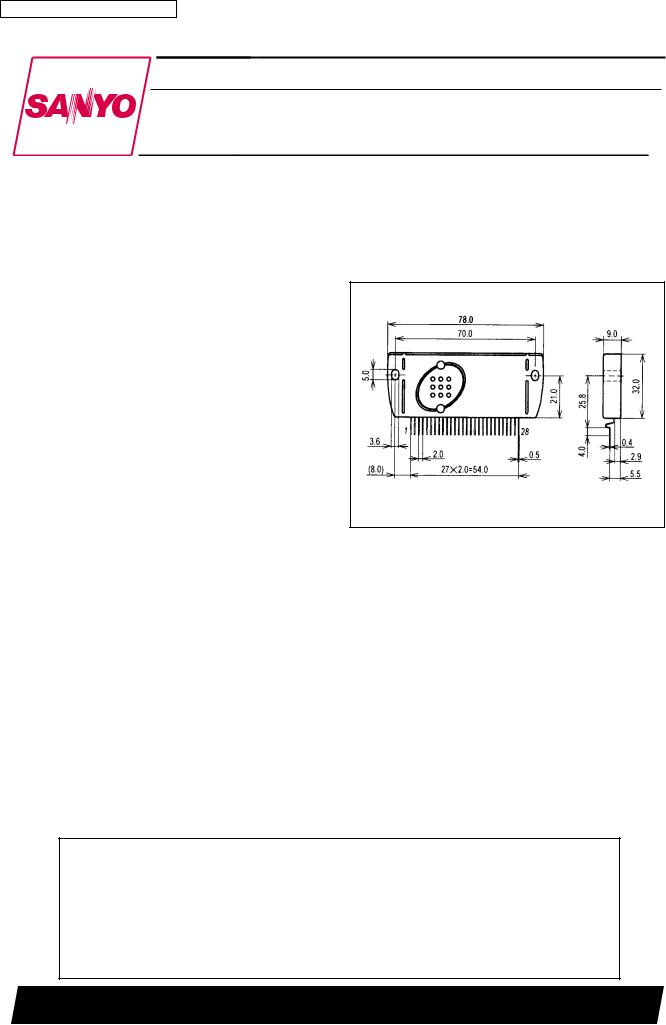
Ordering number : ENN*7376
Thick-Film Hybrid IC
STK403-450
Six-Channel Class AB Audio Power Amplifier IC
30 W ×6 Channels
Preliminary
Overview
The STK403-400 series products are audio power amplifier hybrid ICs that consist of optimally-designed discrete component power amplifier circuits that have been miniaturized using SANYO’s unique insulated metal substrate technology (IMST). The adoption of a newlydeveloped low thermal resistance substrate allows this product to integrate six power amplifier channels in a single compact package. The adoption of a standby circuit in this device allows it to reduce impulse noise significantly as compared to earlier Sanyo products, in particular, the STK402-*00 series products.
Features
•Series of pin compatible power amplifiers ranging from 30 W/ch to 45 W/ch (10%/1 kHz) devices. The same printed circuit board can be used depending on the output power grade.
•Miniature packages
—78.0 mm × 32.0 mm × 9.0 mm *
*: Not including the pins.
•Output load impedance: RL = 6 Ω
•Allowable load shorted time: 0.3 seconds
•Supports the use of standby and muting circuits.
Package Dimensions
unit: mm
4202-SIP28
[STK403-450]
SANYO: SIP28
 Any and all SANYO products described or contained herein do not have specifications that can handle applications that require extremely high levels of reliability, such as life-support systems, aircraft’s control systems, or other applications whose failure can be reasonably expected to result in serious physical and/or material damage. Consult with your SANYO representative nearest you before using any SANYO products described or contained herein in such applications.
 SANYO assumes no responsibility for equipment failures that result from using products at values that exceed, even momentarily, rated values (such as maximum ratings, operating condition ranges, or other parameters) listed in products specifications of any and all SANYO products described or contained herein.
SANYO Electric Co.,Ltd. Semiconductor Company
TOKYO OFFICE Tokyo Bldg., 1-10, 1 Chome, Ueno, Taito-ku, TOKYO, 110-8534 JAPAN
21604TN (OT) No. 7376-1/8
 Loading...