

Samsung S3C8837, S3C8835, S3P8837 Datasheet

S3C8835/C8837/P8837 PRODUCT OVERVIEW
1 PRODUCT OVERVIEW
SAM87 PRODUCT FAMILY
Samsung's SAM87 family of 8-bit single-chip CMOS microcontrollers offers a fast and efficient CPU, a wide
range of integrated peripherals, and various mask-programmable ROM sizes. Important CPU features include:
— Efficient register-oriented architecture
— Selectable CPU clock sources
— Release by interrupt of Idle and Stop power-down modes
— Built-in basic timer circuit with watchdog function
A sophisticated interrupt structure recognizes up to eight interrupt levels. Each level can have one or more
interrupt sources and vectors. Fast interrupt processing (within a minimum six CPU clocks) can be assigned to
specific interrupt levels.
S3C8835/C8837/P8837
The S3C8835 microcontroller has 16 K bytes of on-chip program memory and the S3C8837 has 24 K bytes. Both
chips have a 272-byte general-purpose internal register file. The interrupt structure has seven interrupt sources
with six interrupt vectors. The CPU recognizes six interrupt priority levels.
Using a modular design approach, the following peripherals were integrated with the SAM87 core to make the
S3C8835/C8837/P8837 suitable for use in color television and other types of screen display applications:
— Four programmable I/O ports (26 pins total: 16 general-purpose I/O pins; 8 n-channel, open-drain output pins)
— 2 channel A/D converter (4-bit resolution)
— 14-bit PWM output (one channels: push-pull type)
— Basic timer (BT) with watchdog timer function
— One 8-bit timer/counter (T0) with interval timer
— One 8-bit general-purpose timer/counter (TA) with prescalers
— On-screen display (OSD) with a wide range of programmable features including halftone control signal output
The S3C8835/C8837 are available in a versatile 42-pin SDIP package.
OTP
The S3C8835/C8837 microcontroller is also available in OTP (One Time Programmable) version, S3P8837.
S3P8837 microcontroller has an on-chip 24K-byte one-time-programmable EPROM instead of masked ROM.
The S3P8837 is comparable to S3C8835/C8837, both in function and in pin configuration.
1-1

PRODUCT OVERVIEW S3C8835/C8837/P8837
FEATURES
CPU
• SAM87 CPU core
Memory
• 16-K byte (S3C8835) or 24K- byte (S3C8837)
internal program memory
• 272-byte general-purpose register area
Instruction Set
• 78 instructions
• IDLE and STOP instructions added for powerdown modes
Instruction Execution Time
• 750 ns (minimum) with an 8-MHz CPU clock
Interrupts
• 7 interrupt sources with 6 vectors
• 6 interrupt levels
• Fast interrupt processing for select levels
General I/O
Pulse Width Modulation Module
• 14-bit PWM with one-channel output (push-pull
type)
• PWM counter and data capture input pin
• Frequency: 5.859 kHz to 23.437 kHz with a
6-MHz CPU clock
On-Screen Display (OSD)
• Video RAM: 252 × 12 bits
• Character generator ROM: 256 × 18 × 16 bits
(256 display characters: fixed: 2, variable: 254)
• 252 display positions (12 rows × 21 columns)
• 16-dot × 18-dot character resolution
• 16 different character sizes
• Eight character colors
• Vertical direction fade-in/fade-out control
• Eight colors for character and frame background
• Halftone control signal output; selectable for
individual characters
• Synchronous polarity selector for H-sync and
V-sync input
• Four I/O ports (26 pins total)
• Six open-drain pins for up to 6-volt loads
• Two open-drain pins for up to 5-volt loads
8-Bit Basic Timer
• Three selectable internal clock frequencies
• Watchdog or oscillation stabilization function
Timer/Counters
• One 8-bit timer/counter (T0) with three internal
clocks and interval timer mode.
• One general-purpose 8-bit timer/counters with
interval timer mode (timer A)
A/D Converter
• Two analog input pins; 4-bit resolution
• 3.125 µs conversion time (8-MHz CPU clock)
Oscillator Frequency
• 5-MHz to 8-MHz external crystal oscillator
• Maximum 8-MHz CPU clock
Operating Temperature Range
• – 20°C to + 85°C
Operating Voltage Range
• 4.5 V to 5.5 V
Package Type
• 42-pin SDIP
1-2
S3C8835/C8837/P8837 PRODUCT OVERVIEW
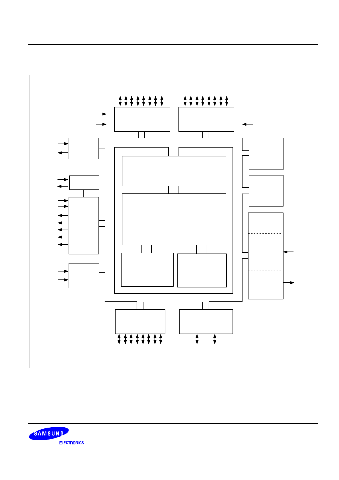
BLOCK DIAGRAM
X
OSC
OSC
H-sync
V-sync
Vgreen
Vblue
Vblank
OSDHT
ADC0
ADC1
X
IN
OUT
IN
OUT
Vred
RESET
INT0 - INT1
MAIN
OSC
L-C OSC
ON-
SCREEN
DISPLAY
4-BIT
ADC
P0.0 - P0.7
PORT 0 PORT 1
SAM87 BUS
PORT I/O and INTERRUPT
CONTROL
SAM87 CPU
16KB ROM (8835)
24KB ROM (8837)
SAM87 BUS
P1.0 - P1.7
272-BYTE
REGISTER FILE
TEST
TIMER A
TIMER 0
PWM
BLOCK
PWM
COUNTER
and DATA
CAPTURE
14-BIT
PWM
CAPA
PWM0
PORT 2
P2.0 - P2.7
Figure 1-1. Block Diagram
PORT 3
P3.0 - P3.1
1-3

PRODUCT OVERVIEW S3C8835/C8837/P8837
PIN ASSIGNMENTS
P2.5/PWM0
P2.1
P2.2(
SCL
P2.3(
SDA
P2.4
P2.0
P2.6
P1.7
P3.0/ADC0
P3.1/ADC1
P0.6
P0.7
TEST
P1.0/INT0
P1.1/INT1
P1.2
P1.3
P1.4
P1.5
P1.6
P2.7/OSDHT
1
2
)
3
)
4
5
6
7
8
9
10
11
12
13
S3C8835
S3C8837
42-PIN SDIP
(Top View)
14
15
16
17
18
19
20
21
42
41
40
39
38
37
36
35
34
33
32
31
30
29
28
27
26
25
24
23
22
P0.0
P0.1
P0.2
P0.3
P0.4
V
SS2
CAPA
P0.5
V
DD
RESET
X
OUT
X
IN
V
SS1
OSC
OUT
OSC
IN
V-sync
H-sync
Vblank
Vred
Vgreen
Vblue
1-4
Figure 1-2. S3C8835/C8837/P8837 Pin Assignment Diagram

S3C8835/C8837/P8837 PRODUCT OVERVIEW
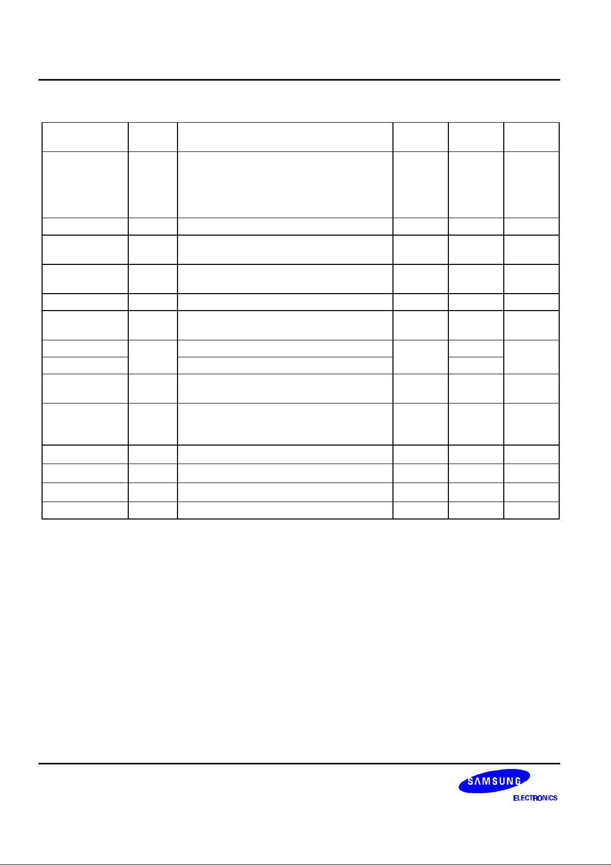
Table 1-1. S3C8835/C8837 Pin Descriptions
Pin Name Pin
Pin Description Circuit
Type
P0.0–P0.7 I/O General I/O port (8-bit), configurable for
digital input or push-pull output.
P1.0–P1.1 I/O General I/O port (2-bit), configurable for
digital input or n-channel open-drain output.
P1.0–P1.1 can withstand up to 6-volt loads.
Multiplexed for alternative use as external
interrupt inputs INT0–INT1.
P1.2–P1.5 General I/O port (4-bit), configurable for
digital input or n-channel open-drain output.
P1.2–P1.5 can withstand up to 6-volt loads.
High current port (10mA).
P1.6–P1.7 General I/O port (2-bit), configurable for
digital input or push-pull output.
P2.0–P2.4,
P2.6
I/O General I/O port (6-bit). I/O mode or
n-channel open-drain, push-pull output
mode is software configurable. Pins can
withstand up to 5-volt loads.
P2.2: OTP serial clock pin
P2.3: OTP serial data pin
P2.5, P2.7 General I/O port (2-bit). I/O mode or
n-channel open-drain, push-pull output
mode is software configurable. Pins can
withstand up to 5-volt loads.
Each pin has an alternative function.
P2.5: PWM0 (14-bit PWM output)
P2.7: OSDHT (Halftone signal output)
Type
Pin
Numbers
Share
Pins
3 11–12, 35,
38–42
7 14–15 INT0–INT1
5 16–19
3 20, 8
2 2–7
2 1, 21 PWM0
OSDHT
1-5
PRODUCT OVERVIEW S3C8835/C8837/P8837
Table 1-1. S3C8835/C8837 Pin Descriptions (Continued)
Pin Name Pin
Type
P3.0–P3.1 I/O General I/O port (2 bits), configurable for
digital input or n-channel open-drain output.
Pin Description Circuit
Type
6 9–10 ADC0
Pin
Numbers
Share
Pins
ADC1
P3.0–P3.1 can withstand up to 5-volt loads.
Multiplexed for alternative use as external
interrupt inputs ADC0–ADC1.
PWM0 O Output pin for 14-bit PWM0 circuit 2 1 P2.5
ADC0–ADC1 I Analog inputs for 4-bit A/D converter 6 9,10 P3.0–
P3.1
INT0–INT1 I External interrupt input pins 7 14,15 P1.0–
P1.1
OSDHT O Halftone control signal output for OSD 2 21 P2.7
Vblue, Vgreen
Vred, Vblank
O Digital blue, green, red, and video blank
signal outputs for OSD
4 22–25 –
H-sync I H-sync input for OSD 8 26 –
V-sync V-sync input for OSD 27
OSC
IN,
OSC
OUT
I, O L-C oscillator pins for OSD clock frequency
– 28,29 –
generation
TEST I
0 V: Normal operation mode
– 13 –
5 V: Factory test mode
12.5 V: OTP write mode
X
IN, XOUT
RESET
V
DD, VSS1, VSS2
I, O System clock pins – 31, 32 –
I System reset input pin 1 33 –
– Power supply pins – 13 –
CAPA I Input for capture A module 8 26 –
1-6
 Loading...