

Samsung S3C8615, S3C8618, S3P8615 Datasheet
S3C8618/C8615/P8615 PRODUCT OVERVIEW
1 PRODUCT OVERVIEW
SAM8 PRODUCT FAMILY
Samsung's SAM8 family of 8-bit single-chip CMOS microcontrollers offers a fast and efficient CPU, a wide range
of integrated peripherals, and various mask-programmable ROM sizes. Important CPU features include:
— Efficient register-oriented architecture
— Selectable CPU clock sources
— Idle and Stop power-down mode release by interrupt
— Built-in basic timer with watchdog function
A sophisticated interrupt structure recognizes up to eight interrupt levels. Each level can have one or more
interrupt sources and vectors. Fast interrupt processing (within a minimum six CPU clocks) can be assigned to
specific interrupt levels.
S3C8618/C8615/P8615 MICROCONTROLLERS
The S3C8618/C8615/P8615 single-chip 8-bit
microcontroller is based on the powerful SAM8 CPU
architecture. The internal register file is logically
expanded to increase the on-chip register space. The
S3C8618/C8615/P8615 have 8/16 K bytes of on-chip
program ROM.
Following Samsung's modular design approach, the
following peripherals were integrated with the SAM8
core:
— Four programmable I/O ports (total 28 pins)
— One 8-bit basic timer for oscillation stabilization
and watchdog functions
— One 8-bit general-purpose timer/counter with
selectable clock sources
— One 8-bit counter with selectable clock sources,
including Hsync or Csync input
— One 8-bit timer for interval mode
— PWM block with seven 8-bit PWM circuits
— Sync processor block (for Vsync and Hsync I/O,
Csync input, and Clamp signal output)
— Multi master IIC-bus with DDC support.
The S3C8618/C8615/P8615 are a versatile
microcontroller that is ideal for use in multi-sync
monitors or in general-purpose applications that
require sophisticated timer/counter, PWM, sync
signal processing, and multi-master IIC-bus support
with DDC. It is available in a 42-pin SDIP or a 44-pin
QFP package.
Figure 1-1. S3C8618/C8615/P8615
Microcontrollers
1-1

PRODUCT OVERVIEW S3C8618/C8615/P8615
FEATURES
CPU
• SAM8 CPU core
Memory
• 8/16-Kbyte internal program memory (ROM)
• 272-byte general-purpose register area
Instruction Set
• 78 instructions
• IDLE and STOP instructions added for powerdown modes
Instruction Execution Time
• 500 ns minimum (with 12 MHz CPU clock)
Interrupts
• Nine interrupt sources
• Nine interrupt vectors
• Six interrupt levels
• Fast interrupt processing for a select level
General I/O
• Four I/O ports (total 28 pins):
8-Bit Basic Timer
• Programmable timer for oscillation stabilization
interval control or watchdog timer functions
• Three selectable internal clock frequencies
Timer/Counters
• One 8-bit general-purpose timer/counter with
programmable operating modes and the following
clock source options:
— Two selectable internal clock frequencies
• One 8-bit timer with interval operating mode
• One 8-bit counter with the following clock source
options:
— Two selectable internal clock frequencies
— Hsync (or Csync) input from the sync
processor block
— External clock source
Pulse Width Modulator
• Seven 8-bit PWM modules:
— 8-bit basic frame
— Four push-pull and three n-channel,
open-drain output channels
— Selectable clock frequencies: 46.875 kHz at
12 MHz fosc.
Sync Processor
• Detection of sync input signals (Vsync-I, Hsync-I,
and Csync-I)
• Sync signal separation and output (Hsync-O,
Vsync-O, and Clamp-O)
• Pseudo sync signal output
• Programmable clamp signal output
DDC and Multi-Master IIC-Bus
• Serial peripheral interface
• Support for display data channel (DDC)
Oscillator Frequency
• 6 MHz to 12 MHz external crystal oscillator
• Interval Max. 12MHz CPU clock
Operating Temperature Range
• – 40°C to + 85°C
Operating Voltage Range
• 4.5 V to 5.5 V
Package Types
• 42-pin SDIP, 44-pin QFP
1-2

S3C8618/C8615/P8615 PRODUCT OVERVIEW
BLOCK DIAGRAM
XIN
X
OUT
PWM0
PWM1
•
•
•
PWM6
Vsync-I
Hsync-I
Csync-I
Vsync-O
Hsync-O
Clamp-O
T0CAP
RESET
INT0-INT2
CESSOR
TIMER 0
MAIN
OSC
8-BIT
PWM
(7-CH)
SYNC
PRO-
P0.0–P0.7/INT0-INT2
PORT 0
INTERNAL BUS
I/O PORT and INTERRUPT
CONTROL
SAM8 CPU
8/16-KBYTE MASK ROM
272-BYTE REGISTER FILE
P2.0–P2.7
PORT 2
TEST
PORT 1
PORT3
DDC and
Multi master
IIC-bus
P1.0–P1.3
P3.0–P3.7
SCL
SDA
8-blt
Counter
(TIMER 1)
T1CK
Interval
timer
(TIMER 2)
Figure 1-2. Block Diagram
1-3

PRODUCT OVERVIEW S3C8618/C8615/P8615
PIN ASSIGNMENTS
P3.1
P3.0
P0.0/INT0
P0.1/INT1
P0.2/INT2
P0.3
P0.4/T0CAP
P0.5/T1CK
VDD
P0.6
P0.7
P1.0
P1.1
P1.2
P1.3
P2.0/PWM0
P2.1/PWM1
P2.2/PWM2
P2.3/PWM3
P2.4/PWM4
P2.5/PWM5
1
2
3
4
5
6
7
8
9
10
11
12
13
14
15
16
17
18
19
20
21
S3C8618/8615
42-SDIP
(Top View)
42
41
40
39
38
37
36
35
34
33
32
31
30
29
28
27
26
25
24
23
22
P3.2
VSS2
P3.3
P3.4
P3.5
P3.6
P3.7
RESET
XOUT
XIN
VSS1
P2.7/Csync-I
Hsync-I
Vsync-I (VCLK)
Clamp-O
Hsync-O
Vsync-O
SCL
SDA
TEST
P2.6/PWM6
1-4
Figure 1-3. Pin Assignment Diagram (42-SDIP Package)

S3C8618/C8615/P8615 PRODUCT OVERVIEW
P2.0/PWM0
P1.3
P1.2
P1.1
P1.0
P0.7
P0.6
VDD
P0.5/T1CK
P0.4/T0CAP
P0.3
4443424140393837363534
P2.1/PWM1
P2.2/PWM2
P2.3/PWM3
P2.4/PWM4
P2.5/PWM5
N.C.
P2.6/PWM6
TEST
SDA
SCL
Vsync-O
34
35
36
37
38
39
40
41
42
43
44
S3C8618/8615
44-QFP
(Top View)
1234567891011
Vsync-I
Hsync-O
Clamp-O
VSS1
Hsync-I
P2.7/Csync-I
XIN
XOUT
P3.7
RESET
P3.6
Figure 1-4. Pin Assignment Diagram (44-QFP Package)
33
32
31
30
29
28
27
26
25
24
23
P0.2/INT2
P0.1/INT1
P0.0/INT0
P3.0
P3.1
NC
P3.2
VSS2
P3.3
P3.4
P3.5
1-5
PRODUCT OVERVIEW S3C8618/C8615/P8615
PIN DESCRIPTIONS
Table 1-1. S3C8618/C8615/P8615 Pin Descriptions
Pin
Names
P0.0
P0.1
P0.2
P0.3
P0.4
Pin
Type
Pin
Description
I/O General-purpose, 8-bit I/O port. Share
functions include three external interrupt
inputs, I/O for timers 0 and 1. You can
selectively configure port 0 pins to input or
output mode.
P0.5
P0.6
P0.7
P1.0–P1.3 I/O General purpose, 8-bit I/O port. You can
selectively configure port 1 pins to input or
push-pull output mode.
P2.0
P2.1
P2.2
P2.3
P2.4
I/O General purpose, 8-bit I/O port. You can
selectively configure port 2 pins to input or
output mode. The port 2 pin circuit are
designed to push-pull PWM output and
Csync signal input.
P2.5
P2.6
P2.7
P3.0–P3.7 I/O General-purpose, 8-bit I/O port. You can
selectively configure port 3 pins to input or
output mode.
Hsync-I
Vsync-I
Clamp-O
Hsync-O
Vsync-O
SCL
SDA
V
DD
V
, V
SS1
XIN, X
OUT
RESET
SS2
I
The pins are sync processor signal I/O and
I
IIC-bus clock and data I/O
O
O
O
I/O
I/O
– Power supply pins – 9
– System clock input and output pins – 33, 34 –
I System reset pin B 35 –
TEST I Factory test pin input
0 V: normal operation
5 V: factory test mode
Circuit
Type
SDIP Pin
Numbers
Functions
D-1 3
4
5
6
7
8
10
11
D-1 12–15 –
D-1
D-1
D-1
D-1
E-1
E-1
E-1
D-1
16
17
18
19
20
21
22
31
E 2, 1, 42,
40–36
A
A
A
A
A
G-3
G-3
30
29
28
27
26
25
24
32, 41
– 23 –
Shared
INT0
INT1
INT2
T0CAP
T1CK
PWM0
PWM1
PWM2
PWM3
PWM4
PWM5
PWM6
Csync-I
–
–
–
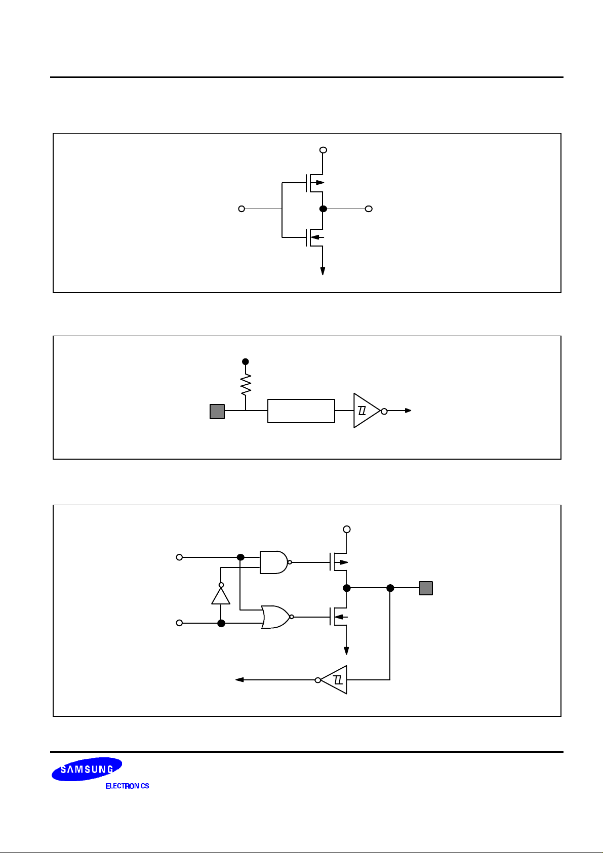
NOTE: See ‘Pin Circuit Diagrams’ on next two pages for detailed information on circuit types A, B, D-1, E, E-1,and G-3.
1-6
S3C8618/C8615/P8615 PRODUCT OVERVIEW
PIN CIRCUITS
Vdd
Vss
Figure 1-5. Pin Circuit Type A
Data or
Other
function
Output
Disable
Vdd
280 K
Ω
Noise Filter
RESET
Figure 1-6. Pin Circuit Type B (RESETRESET)
Vdd
Vss
Output
Digital Input
or TTL Input
Figure 1-7. Pin Circuit Type D-1
1-7
 Loading...