

Page 1

USER’S MANUAL
S3C84I8X/F84I8X/
C84I9X/F84I9X
8-BIT CMOS MICROCONTROLLERS
June, 2007
REV 2.00
Confidential Proprietary of Samsung Electronics Co., Ltd
Copyright © 2007 Samsung Electronics, Inc. All Rights Reserved
Page 2

Important Notice
The information in this publication has been carefully
checked and is believed to be entirely accurate at
the time of publication. Samsung assumes no
responsibility, however, for possible errors or
omissions, or for any consequences resulting from
the use of the information contained herein.
Samsung reserves the right to make changes in its
products or product specifications with the intent to
improve function or design at any time and without
notice and is not required to update this
documentation to reflect such changes.
This publication does not convey to a purchaser of
semiconductor devices described herein any license
under the patent rights of Samsung or others.
Samsung makes no warranty, representation, or
guarantee regarding the suitability of its products for
any particular purpose, nor does Samsung assume
any liability arising out of the application or use of
any product or circuit and specifically disclaims any
and all liability, including without limitation any
consequential or incidental damages.
S3C84I8X/F84I8X/C84I9X/F84I9X 8-Bit CMOS Microcontrollers
User's Manual, Revision 2.00
Publication Number: 22-S3-C84I8X/F84I8X/C84I9X/F84I9X-062007
"Typical" parameters can and do vary in different
applications. All operating parameters, including
"Typicals" must be validated for each customer
application by the customer's technical experts.
Samsung products are not designed, intended, or
authorized for use as components in systems
intended for surgical implant into the body, for other
applications intended to support or sustain life, or for
any other application in which the failure of the
Samsung product could create a situation where
personal injury or death may occur.
Should the Buyer purchase or use a Samsung
product for any such unintended or unauthorized
application, the Buyer shall indemnify and hold
Samsung and its officers, employees, subsidiaries,
affiliates, and distributors harmless against all
claims, costs, damages, expenses, and reasonable
attorney fees arising out of, either directly or
indirectly, any claim of personal injury or death that
may be associated with such unintended or
unauthorized use, even if such claim alleges that
Samsung was negligent regarding the design or
manufacture of said product.
Copyright © 2006-2007 Samsung Electronics Co., Ltd.
All rights reserved. No part of this publication may be reproduced, stored in a retrieval system, or transmitted in
any form or by any means, electric or mechanical, by photocopying, recording, or otherwise, without the prior
written consent of Samsung Electronics.
Samsung Electronics' microcontroller business has been awarded full ISO-14001
certification (BSI Certificate No. FM24653). All semiconductor products are designed
and manufactured in accordance with the highest quality standards and objectives.
Samsung Electronics Co., Ltd.
San #24 Nongseo-Dong, Giheung-Gu
Yongin-City, Gyeonggi-Do, Korea
C.P.O. Box #37, 446-711
TEL: (82)-(31)-209-5238
FAX: (82)-(31)-209-6494
Home Page: http://www.samsung.com
Printed in the Republic of Korea
Page 3

NOTIFICATION OF REVISIONS
ORIGINATOR: Samsung Electronics, LSI Development Group, Gi-Heung, South Korea
PRODUCT NAME: S3C84I8X/F84I8X/C84I9X/F84I9X 8-bit CMOS Microcontroller
DOCUMENT NAME: S3C84I8X/F84I8X/C84I9X/F84I9X User's Manual, Revision 2.00
DOCUMENT NUMBER: 22- S3-C84I8X/F84I8X/C84I9X/F84I9X- 062007
EFFECTIVE DATE: June, 2007
SUMMARY: As a result of additional product testing and evaluation, some specifications
published in S3C84I8X/F84I8X/C84I9X/F84I9X User's Manual, Revision 1.00,
have been changed. These changes for in S3C84I8X/F84I8X/C84I9X/F84I9X
microcontroller, which are described in detail in the
Revision Descriptions section below, are related to the followings:
— Chapter 4. Control Registers
DIRECTIONS: Please note the changes in your copy (copies) of the
S3C84I8X/F84I8X/C84I9X/F84I9X User’s Manual,
Revision 1.00. Or, simply attach the Revision Descriptions of the next page to
S3C84I8X/F84I8X/C84I9X/F84I9X User’s Manual, Revision 1.00.
REVISION HISTORY
Revision Description of Change Refer to
1.00 First edition. T.H. Kim Nov, 2006
2.00 Second edition Page 4-17 T.H. Kim June, 2007
Author(s)
Date
Page 4
REVISION DESCRIPTIONS
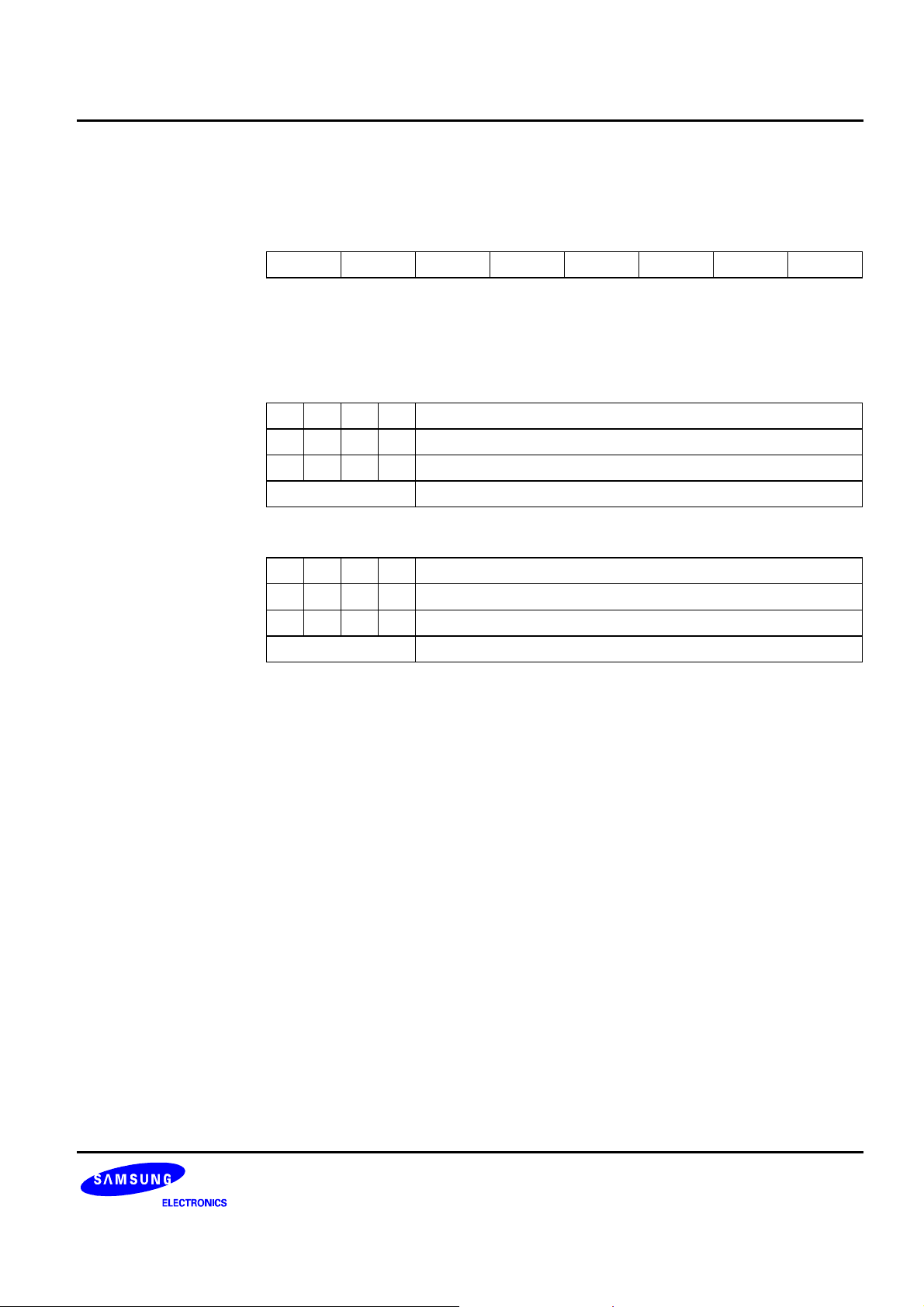
1. Chapter 4. Control Registers
LPOT — LCD Port Control Register F7H Set 1, Bank1
Bit Identifier .7 .6 .5 .4 .3 .2 .1 .0
RESET Value
Read/Write
.7
.6–.4 SEG4-SEG19 and COM0-COM3 Selection Bit
.3 SEG3/P2.7 Selection Bit
.2 SEG2/P2.6 Selection Bit
.1 SEG1/P2.5 Selection Bit
.0 SEG0/P2.4 Selection Bit
– 0 0 0 0 0 0 0
– R/W R/W R/W R/W R/W R/W R/W
Not used for S3C84I8X/F84I8X/C84I9X/F84I9X
SEG4-7 SEG8-11 SEG12-15 SEG16-19/
COM7-COM4
P3.0-P3.3 P3.4-P3.7 P4.0-P4.3 P4.4-P4.7 P0.0-P0.3
0 0 0
0 1 0
1 0 0
1 0 1
1 1 0
1 1 1
0
Normal I/O port
1
SEG port
0
Normal I/O port
1
SEG port
0
Normal I/O port
1
SEG port
0
Normal I/O port
1
SEG port
Port Port Port Port Port
Port Port Port Port COM
SEG SEG SEG SEG/COM COM
Port SEG SEG SEG/COM COM
Port Port SEG SEG/COM COM
Port Port Port SEG/COM COM
COM0-3
Page 5

USER'S MANUAL
ERRATA
This document contains the corrections of errors,
typos and omissions in the following document.
Samsung 8-bit CMOS S3C84I8X/F84I8X/C84I9X/F84I9X
Microprocessor User's Manual
Document Number: 02-2.00-S3-C84I8X/F84I8X/C84I9X/F84I9X-062007
Publication: June 2007
Page 6
S3C84I8X/F84I8X/C84I9X/F84I9X_ERRATA_REV 2.00 USER’S MANUAL ERRATA
ERRATA (VER 2.00)
Samsung 8-bit CMOS S3C84I8X/F84I8X/C84I9X/F84I9X Microprocessor User’s Manual
Document Number: 02-2.00-S3- C84I8X/F84I8X/C84I9X/F84I9X-062007
Publication: June 2007
1. PIN ASSIGNMENT (PAGE 1-4)
INT0/TAOUT/P1.0
INT1/BUZ/TACK/P1.1
SDAT/INT2/TACAP/P1.2
SCLK/INT3/T1OUT1/P1.3
VDD
VSS
Xout
Xin
Vpp/TEST
Xtin
Xtout
P4.1/SEG13
P 4.7/SEG 19/C OM7
P 4.6/SEG 18/C OM6
P4.5/S EG17/C OM5
4443424140393837363534
1
2
3
4
5
6
7
8
9
10
11
S3C84I9X/F84I9X
S3C84I8X/F84I8X
(44-QFP)
1213141516171819202122
RESET
n
P4.2/S EG14
P4.3/S EG15
P4 .4/SEG1 6/C OM 4
Top View
P4.0/SEG12
P3.7/SEG11
P3.5/SEG9
P3.6/SEG10
33
32
31
30
29
28
27
26
25
24
23
P3.4/SEG8
P3.3/SEG7
P3.2/SEG6
P3.1/SEG5
P3.0/SEG4
P0.3/COM3/AD3
P0.2/COM 2/AD2
P0.1/COM 1/AD1
P0.0/COM0/AD0
Avss
Avref
SI/AD 7/P2. 3
Rx/SEG2 /P2.6
SO/S EG0/P2.4
T1CK1/AD5 /P 1.4
T1CAP1/AD6/P1.5
T1OUT0/AD4/P2.2
PWM/T1CAP0/P2.1
TBPWM/T1CK0/P2.0
Figure 1-2. S3C84I8X/F84I8X/C84I9X/F84I9X Pin Assignment (44-pin QFP)
1
TX/S EG3/P2.7
SCK/ S EG1/P2 .5
Page 7
USER’S MANUAL ERRATA S3C84I8X/F84I8X/C84I9X/F84I9X_ERRATA_REV 2.00
2. PIN ASSIGNMENT (PAGE 1-5)
SEG14/P4.2
SEG15P4.3
SEG16/COM4/P4.4
SEG17/COM5/P4.5
COM6/SEG18/P4.6
COM7/SEG19/P4.7
INT0/TAOUT/P1.0
INT1/BUZ/TACK/P1.1
SDAT/INT2/TACAP/P1.2
SCLK/INT3/T1OUT1/P1.3
VDD
VSS
Xout
Xin
Vpp/TEST
XTin
XTout
nRESET
TBPWM/T1CK0/P2.0
PWM/T1CAP0/P2.1
T1OUT0/AD4/P2.2
1
2
3
4
5
6
7
S3C84I9X/F84I9X
8
9
10
11
12
13
14
15
16
17
18
19
20
21
Top View
(42-SDIP)
42
41
40
39
38
37
36
35
34
33
32
31
30
29
28
27
26
25
24
23
22
P4.1/SEG13
P4.0/SEG12
P3.7/SEG11
P3.6/SEG10
P3.5/SEG9
P3.4/SEG8
P3.3/SEG7
P3.2/SEG6
P3.1/SEG5
P3.0/SEG4
AD3/COM3/P0.3
AD2/COM2/P0.2
AD1/COM1/P0.1
AD0/COM0/P0.0
AVss
AVref
P2.7/SEG3/TxD
P2.6/SEG2/RxD
P2.5/SEG1/SCK
P2.4/SEG0/SO
P2.3/AD7/SI
Figure 1-3. S3C84I9X/F84I9X Pin Assignment (42-pin SDIP)
2
Page 8
S3C84I8X/F84I8X/C84I9X/F84I9X_ERRATA_REV 2.00 USER’S MANUAL ERRATA
3. PIN ASSIGNMENT (PAGE 1-14)
V
DD
V
DD
Data
Open Drain EN
Data
LCD Out EN
SEG
Type H-4
Output Disable
Normal Input
P-CH
N-CH
Circuit
Figure 1-12. Pin Circuit Type H-17 (P3.0–P3.7, P4.0–P4.)
VDD
VDD
P-CH
Pull-up
Enable
I/O
Pull-up
Enable
I/O
LCD Out EN
Output Disable
Normal Input
N-CH
SEG
Circuit
Type H-4
Figure 1-13. Pin Circuit Type H-18 (2.4–P2.7)
3
Page 9

USER’S MANUAL ERRATA S3C84I8X/F84I8X/C84I9X/F84I9X_ERRATA_REV 2.00
4. REGISTER ARCHITECTURE (PAGE 2-5)
64
Bytes
32
Bytes
FFH
E0H
DFH
D0H
CFH
C0H
13H
Set1
Bank 1
Bank 0
System and
Peripheral Control Registers
(Register Addressing Mode)
System and
Peripheral Control Registers
(Register Addressing Mode)
General Purpose Register
(Register Addressing Mode)
Page 2
FFH
E0H
192
Bytes
FFH
C0H
BFH
Page 1
Page 0
Set 2
General-Purpose
Data Registers
(Indirect Register, Indexed
Mode, and Stack Operations)
256
Bytes
Prime
Data Registers
(All Addressing Modes)
LCD Display Registers
00H
00H
NOTE: Page2's 00H~13H is used for LCD Display Registers(Write-only).
Figure 2-3. Internal Register File Organization of S3F84I9X/C84I9X
4
Page 10
S3C84I8X/F84I8X/C84I9X/F84I9X_ERRATA_REV 2.00 USER’S MANUAL ERRATA
64
Bytes
32
Bytes
FFH
E0H
DFH
D0H
CFH
C0H
13H
00H
Set1
Bank 1
Bank 0
System and
Peripheral Control Registers
(Register Addressing Mode)
System and
Peripheral Control Registers
(Register Addressing Mode)
General Purpose Register
(Register Addressing Mode)
Page 2
LCD Display Registers
FFH
E0H
192
Bytes
FFH
C0H
BFH
00H
Page 0
Set 2
General-Purpose
Data Registers
(Indirect Register, Indexed
Mode, and Stack Operations)
256
Bytes
Page 0
Prime
Data Registers
(All Addressing Modes)
NOTE: Page2's 00H~13H is used for LCD Display Registers(Write only)
Figure 2-4. Internal Register File Organization of S3F84I8X/C84I8X
5
Page 11

USER’S MANUAL ERRATA S3C84I8X/F84I8X/C84I9X/F84I9X_ERRATA_REV 2.00
5. REGISTER PAGE POINTER (PAGE 2-7)
Register Page Pointer (PP)
DFH ,Set 1, R/W
LSBMSB .7 .6 .5 .4 .3 .2 .1 .0
Destination register page selection bits:
0000 0000
0001
0002
NOTE:
Destination: Page 0
Destination: Page 1 Source: Page 1
Destination: Page 2
In the S3C84I9X/F84I9X microcontroller, page 0,1,2 are implemented.
In the S3C84I8X/F84I8X microcontroller, page 0,2 are implemented.
A hardware reset operation writes the 4-bit destination and source values shown
above to the register page pointer(00H). These values should be modified to
other pages
Source register page selection bits:
Source: Page 0
0001
0002
Source: Page 2
Figure 2-5. Register Page Pointer (PP)
6
Page 12
S3C84I8X/F84I8X/C84I9X/F84I9X_ERRATA_REV 2.00 USER’S MANUAL ERRATA
6. CONTROL REGISTERS (PAGE 4-19)
P0CON — Port 0 Control Register (High Byte) E6H Set 1, Bank0
.7–.6 P0.3/AD3/COM3 Configration Bits
.5–.4 P0.2/AD2/COM2 Configration Bits
.3–.2 P0.1/ AD1/COM1 Configration Bits
.1–.0 P0.0/ AD0/COM0 Configration Bits
0 0 Input mode
0 1 Input mode with pull-up
1 0 Push-pull output mode
1 1 Alternative function mode; AD3 input
0 0 Input mode
0 1 Input mode with pull-up
1 0 Push-pull output mode
1 1 Alternative function mode; AD2 input
0 0 Input mode
0 1 Input mode with pull-up
1 0 Push-pull output mode
1 1 Alternative function mode; AD1 input
0 0 Input mode
0 1 Input mode with pull-up
1 0 Push-pull output mode
1 1 Alternative function mode; AD0 input
NOTE: If you want to use P0 as a LCD port, you must set LPOT register appropriately.(Refer to Ex .2 below)
If you want to use P0 as a Normal I/O or Alternative function(ADC0~ADC3), you must set LPOT register
appropriately. (Refer to Ex. 1 below)
For example,
(1) LD LPOT,#00000000B ; P0.0~P0.3 is Normal I/O or Alternative function(ADC0~ADC3).
(2) LD LPOT,#01001111B ; P0.0~P0.3 is LCD port.
For more detail, please refer to page 9-5
7
Page 13

USER’S MANUAL ERRATA S3C84I8X/F84I8X/C84I9X/F84I9X_ERRATA_REV 2.00
7. CONTROL REGISTERS (PAGE 4-24)
P2CONH — Port 2 Control Register (High Byte) ECH Set 1, Bank0
.7–.6 P2.7/SEG3/TxD Configration Bits
.5-.4 P2.6/SEG2/RxD Configration Bits
.3–.2 P2.5/ SEG1/SCK Configration Bits
.1–.0 P2.4/SEG0/SO Configration Bits
0 0 Input mode
0 1 Alternative function mode: Not used
1 0 Push-pull output mode
1 1 Alternative function mode: TxD output
0 0 Input mode ; RxD input
0 1 Alternative function mode: Not used
1 0 Push-pull output mode
1 1 Alternative function mode: RxD output
0 0 Input mode ; SCK input
0 1 Alternative function mode: Not used
1 0 Push-pull output mode
1 1 Alternative function mode: SCK output
0 0 Input mode
0 1 Alternative function mode: Not used
1 0 Push-pull output mode
1 1 Alternative function mode: SO output
NOTE: If you want to use a P2 as LCD port, you must set LPOT register appropriately. (Refer to Ex. 2 below)
If you want to use a P2 as Normal I/O or Alternative function(SO/SCK/RxD/TxD), you must set LPOT
register appropriately. (Refer to Ex. 1 below)
For example,
(1) LD LPOT,#00000000B ; P2.4~P2.7 is Normal I/O or Alternative function(SO/SCK/RxD/TxD).
(2) LD LPOT,#01001111B ; P2.4~P2.7 is LCD port.
For more detail, please refer to page 9-13
8
Page 14

S3C84I8X/F84I8X/C84I9X/F84I9X_ERRATA_REV 2.00 USER’S MANUAL ERRATA
8. CONTROL REGISTERS (PAGE 4-27)
P3CONH — Port 3 Control Register (High Byte) EEH Set 1, Bank0
.7–.6 P3.7/SEG11 Configration Bits
.5–.4 P3.6/SEG10 Configration Bits
.3–.2 P3.5/ SEG9 Configration Bits
.1–.0 P3.4/ SEG8 Configration Bits
0 0 Input mode
0 1 Input mode with pull-up
1 0 Push-pull output mode
1 1 N-channel open-drain output
0 0 Input mode
0 1 Input mode with pull-up
1 0 Push-pull output mode
1 1 N-channel open-drain output
0 0 Input mode
0 1 Input mode with pull-up
1 0 Push-pull output mode
1 1 N-channel open-drain output
0 0 Input mode
0 1 Input mode with pull-up
1 0 Push-pull output mode
1 1 N-channel open-drain output
NOTE: If you want to use P3 as a LCD port, you must set LPOT register appropriately. (Refer to Ex. 2 below)
If you want to use P3 as a Normal I/O, you must set LPOT register appropriately. (Refer to Ex. 1 below)
For example,
(1) LD LPOT,#00000000B ; P3.4~P3.7 is Normal I/O.
(2) LD LPOT,#01001111B ; P3.4~P3.7 is LCD port.
For more detail, please refer to page 9-16
9
Page 15
USER’S MANUAL ERRATA S3C84I8X/F84I8X/C84I9X/F84I9X_ERRATA_REV 2.00
9. CONTROL REGISTERS (PAGE 4-28)
P3CONL — Port 3 Control Register (Low Byte) EFH Set 1, Bank0
.7–.6 P3.3/ SEG7 Configration Bits
.5–.4 P3.2/ SEG6 Configration Bits
.3–.3 P3.1/ SEG5 Configration Bits
.1–.0 P3.0/ SEG4 Configration Bits
0 0 Input mode
0 1 Input mode with pull-up
1 0 Push-pull output mode
1 1 N-channel open-drain output
0 0 Input mode
0 1 Input mode with pull-up
1 0 Push-pull output mode
1 1 N-channel open-drain output
0 0 Input mode
0 1 Input mode with pull-up
1 0 Push-pull output mode
1 1 N-channel open-drain output
0 0 Input mode
0 1 Input mode with pull-up
1 0 Push-pull output mode
1 1 N-channel open-drain output
NOTE: If you want to use P3 as a LCD port, you must set LPOT register appropriately. (Refer to Ex. 2 below)
If you want to use P3 as a Normal I/O, you must set LPOT register appropriately. (Refer to Ex. 1 below)
For example,
(1) LD LPOT,#00000000B ; P3.0~P3.3 is Normal I/O.
(2) LD LPOT,#01001111B ; P3.0~P3.3 is LCD port.
For more detail, please refer to page 9-16
10
Page 16

S3C84I8X/F84I8X/C84I9X/F84I9X_ERRATA_REV 2.00 USER’S MANUAL ERRATA
10. CONTROL REGISTERS (PAGE 4-29)
P4CONH — Port 4 Control Register (High Byte) F0H Set 1, Bank0
.5–.4 P4.6/ COM6/SEG18 Configration Bits
.3–.3 P4.5/ COM5/SEG17 Configration Bits
.1–.0 P4.4/ COM4/SEG16 Configration Bits
0 0 Input mode
0 1 Input mode with pull-up
1 0 Push-pull output mode
1 1 N-channel open-drain output
0 0 Input mode
0 1 Input mode with pull-up
1 0 Push-pull output mode
1 1 N-channel open-drain output
0 0 Input mode
0 1 Input mode with pull-up
1 0 Push-pull output mode
1 1 N-channel open-drain output
0 0 Input mode
0 1 Input mode with pull-up
1 0 Push-pull output mode
1 1 N-channel open-drain output
NOTE: If you want to use P4 as a LCD port, you must set LPOT register appropriately. (Refer to Ex. 2 below)
If you want to use P4 as a Normal I/O, you must set LPOT register appropriately. (Refer to Ex. 1 below)
For example,
(1) LD LPOT,#00000000B ; P4.4~P4.7 is Normal I/O.
(2) LD LPOT,#01001111B ; P4.4~P4.7 is LCD port.
For more detail, please refer to page 9-19
11
Page 17
USER’S MANUAL ERRATA S3C84I8X/F84I8X/C84I9X/F84I9X_ERRATA_REV 2.00
11. CONTROL REGISTERS (PAGE 4-30)
P4CONL — Port 4 Control Register (Low Byte) F1H Set 1, Bank0
.7–.6 P4.3/ BUZ/SEG15 Configration Bits
.5–.4 P4.2/ SEG14 Configration Bits
.3–.2 P4.1/ SEG13 Configration Bits
.1–.0 P4.0/ SEG12 Configration Bits
0 0 Input mode
0 1 Input mode with pull-up
1 0 Push-pull output mode
1 1 N-channel open-drain output
0 0 Input mode
0 1 Input mode with pull-up
1 0 Push-pull output mode
1 1 N-channel open-drain output
0 0 Input mode
0 1 Input mode with pull-up
1 0 Push-pull output mode
1 1 N-channel open-drain output
0 0 Input mode
0 1 Input mode with pull-up
1 0 Push-pull output mode
1 1 N-channel open-drain output
NOTE: If you want to use P4 as a LCD port, you must set LPOT register appropriately. (Refer to Ex. 2 below)
If you want to use P4 as a Normal I/O, you must set LPOT register appropriately. (Refer to Ex. 1 below)
For example,
(1) LD LPOT,#00000000B ; P4.0~P4.3 is Normal I/O.
(2) LD LPOT,#01001111B ; P4.0~P4.3 is LCD port.
For more detail, please refer to page 9-19
12
Page 18
S3C84I8X/F84I8X/C84I9X/F84I9X_ERRATA_REV 2.00 USER’S MANUAL ERRATA
12. CONTROL REGISTERS (PAGE 4-31)
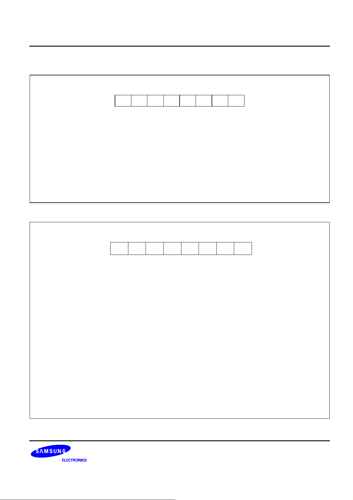
PP — Register Page Pointer DFH Set 1
Bit Identifier .7 .6 .5 .4 .3 .2 .1 .0
RESET Value
Read/Write
Addressing Mode
.7–.4 Destination Register Page Selection Bits
0 0 0 0 Destination: page 0
0 0 0 1 Destination: page 1
0 0 1 0 Destination: page 2
Other values Don’t care
.3–.0 Source Register Page Selection Bits
0 0 0 0 Source: page 0
0 0 0 1 Source: page 1
0 0 1 0 Source: page 2
Other values Don’t care
0 0 0 0 0 0 0 0
R/W R/W R/W R/W R/W R/W R/W R/W
Register addressing mode only
NOTES:
1. In the S3C84I8X/F84I8X microcontroller, the internal register file is configured as two pages (Page 0, Page 2).
The page 0 is used for the general-purpose register file and data register.
2. In the S3C84I9X/F84I9X microcontroller, the internal register file is configured as three pages (Page 0-2)
The page 0 and page 1 are used for the general-purpose register file and data register .
3. The page 2 is used for the LCD display ram and it is a write-only memory.
13
Page 19

USER’S MANUAL ERRATA S3C84I8X/F84I8X/C84I9X/F84I9X_ERRATA_REV 2.00
13. PORT CONTROL REGISTERS (PAGE 9-5)
) PROGRAMMING TIP — To make P0 as Normal I/O or Alternative function
ORG 0100H ; Reset address
START DI
•
•
SB1
LD LPOT,# 00H ; P0 is normal I/O or alternative function
SB0
LD P0CON,#00H ; P0 is input mode
LD P0CON,#055H ; P0 is input pull-up mode
•
LD P0CON,#0AAH ; P0 is Push-pull output mode
LD P0CON,#0FFH ; P0 is ADC input
• SB1
LD LPOT,# 4FH ; P0 is LCD port
SB0
LD P0CON,#0AAH ; If you use P0 as LCD port,P0CON register value doesn’t care
14
Page 20
S3C84I8X/F84I8X/C84I9X/F84I9X_ERRATA_REV 2.00 USER’S MANUAL ERRATA
14. PORT CONTROL REGISTERS (PAGE 9-7)
Port 1 Control Register, High Byte (P1CONH)
E8H, Set1, Bank0, R/W, Reset value="00"
.7 .6 .5 .4 .3 .2 .1 .0MSB LSB
[.7-.4] Not used(must keep always 0)
[.3-.2] P1.5/T1CAP1/AD6 Configuration Bits
0 0 = Input mode; T1CAP1 input
0 1 = Input mode with pull-up; T1CAP1 input
1 0 = Push-pull output mode
1 1 = Alternative function mode: AD6
[.1-.0] P1.4/T1CK1/AD5 Configuration Bits
0 0 = Input mode; T1CK1 input
0 1 = Input mode with pull-up; T1CK1 input
1 0 = Push-pull output mode
1 1 = Alternative function mode: AD5
Figure 9-2. Port 1 High-Byte Control Register (P1CONH)
Port 1 Control Register, Low By te (P 1 CONL)
E9H, Set1, Bank0, R/W, Reset value="00H"
.7 .6 .5 .4 .3 .2 .1 .0MSB LSB
[.7-.6] P1.3/T1OUT1/INT3 Configuration Bits
0 0 = Input mode; Interrupt input (INT3)
0 1 = Input mode with pull-up; Interrupt input (INT3)
1 0 = Push-pull output mode
1 1 = Alternative function mode: T1OUT1 output
[.5-.4] P1.2/TACAP/INT2 Configuration Bits
0 0 = Input mode; Interrupt input (INT2); TACAP
0 1 = Input mode with pull-up; Interrupt input (INT2);TACAP
1 0 = Push-pull output mode
1 1 = Alternative function mode: Not used
[.3-.2] P1.1/TACK/BUZ/INT1 Configuration Bits
0 0 = Input mode; Interrupt input (INT1); TACK
0 1 = Input mode with pull-up ; Interrupt input (INT1); TACK
1 0 = Push-pull output mode
1 1 = Alternative function mode: BUZ output
[.1-.0] P1.0/TAOUT/INT0 Configuration Bits
0 0 = Input mode; Interrupt input (INT0)
0 1 = Input mode with pull-up; Interrupt input (INT0)
1 0 = Push-pull output mode
1 1 = Alternative function mode: TAOUT output
Figure 9-3. Port 1 Low-Byte Control Register (P1CONL)
15
Page 21
USER’S MANUAL ERRATA S3C84I8X/F84I8X/C84I9X/F84I9X_ERRATA_REV 2.00
15. PORT CONTROL REGISTERS (PAGE 9-9)
PORT 2
Port 2 is an 8-bit I/O port with individually configurable pins. Port 2 pins are accessed directly by writing or reading
the port 2 data register, P2 at location E2H in set 1, bank 0. P2.0–P2.7 can serve as digital inputs, outputs (push
pull) or you can configure the following alternative functions:
— General-purpose digital I/O
— Alternative function: SEG0-SEG3, ADC4, ADC7, SI, T1CAP0, T1OUT0, T1CK0, TBPWM, PWM
.
16. PORT CONTROL REGISTERS (PAGE 9-10)
Port 2 Control Register, High Byte (P2CONH)
ECH, Set1, Bank0, R/W, Reset value="00"
.7 .6 .5 .4 .3 .2 .1 .0MSB LSB
[.7-.6] P2.7/SEG3/TxD Configuration Bits
0 0 = Input mode
0 1 = Alternative function mode; Not used
1 0 = Push-pull output mode
1 1 = Alternative function mode; TxD output
[.5-.4] P2.6/SEG2/RxD Configuration Bits
0 0 = Input mode; RxD iput
0 1 = Alternative function mode; Not used
1 0 = Push-pull output mode
1 1 = Alternative function mode; RxD output
[.3-.2] P2.5/SEG1/SCK Configuration Bits
0 0 = Input mode; SCK input
0 1 = Alternative function mode; Not used
1 0 =
Push-pull output mode
1 1 = Alternative function mode; SCK output
[.1-.0] P2.4/SEG0/SO Configuration Bits
0 0 = Input mode
0 1 = Alternative function mode; Not used
1 0 = Push-pull output mode
1 1 = Alternative function mode; SO output
Figure 9-6. Port 2 High-Byte Control Register (P2CONH)
16
Page 22

S3C84I8X/F84I8X/C84I9X/F84I9X_ERRATA_REV 2.00 USER’S MANUAL ERRATA
17. PORT CONTROL REGISTERS (PAGE 9-11)
Port 2 Control Register, Low Byte (P2CONL)
EDH, Set1, Bank0, R/W, Reset value="00"
.7 .6 .5 .4 .3 .2 .1 .0MSB LSB
[.7-.6] P2.3/AD7/SI Configuration Bits
0 0 = Input mode; SI
0 1 = Alternative function mode; Not used
1 0 = Push-pull output mode
1 1 = Alternative function mode; AD7
[.7-.6] P2.2/AD4/T1OUT0 Configuration Bits
0 0 = Input mode
0 1 = Alternative function mode; T1OUT0
1 0 = Push-pull output mode
1 1 = Alternative function mode; AD4
[.7-.6] P2.1/PWM/T1CAP0 Configuration Bits
0 0 = Input mode; T1CAP0
0 1 = Alternative function mode; Not used
1 0 = Push-pull output mode
1 1 = Alternative function mode; PWM
[.7-.6] P2.0/TBPWM/T1CK0 Configuration Bits
0 0 = Input mode;T1CK0
0 1 = Alternative function mode; T1CK0
1 0 = Push-pull output mode
1 1 = Alternative function mode; TBPWM
Figure 9-7. Port 2 Low-Byte Control Register (P2CONL)
17
Page 23

USER’S MANUAL ERRATA S3C84I8X/F84I8X/C84I9X/F84I9X_ERRATA_REV 2.00
18. PORT CONTROL REGISTERS (PAGE 9-13)
) PROGRAMMING TIP — To make P2 as Normal I/O or Alternative function
ORG 0100H ; Reset address
START DI
•
•
SB1
LD LPOT,# 00H ; P2 is normal I/O or alternative function
SB0
LD P2CONH,#00H ; P2 is input mode
LD P2CONH,#0AAH ; P2 is Push-pull output mode
•
LD P2CONH,#0FFH ; P2 is TXOUT,RXOUT,SCK OUT,SO OUT
• SB1
LD LPOT,# 04FH ; P2 is LCD port
SB0
LD P2CONH,#0AAH ; If you use P2 as LCD port,P2CONH register value doesn’t care
LD P2PUR,#00H ; P2PUR is disabled when P2 is used as a LCD port.
18
Page 24

S3C84I8X/F84I8X/C84I9X/F84I9X_ERRATA_REV 2.00 USER’S MANUAL ERRATA
19. PORT CONTROL REGISTERS (PAGE 9-15)
Port 3 Control Register, Low Byte (P3CONL)
EFH, Set1, Bank0, R/W, Reset value="00"
.7 .6 .5 .4 .3 .2 .1 .0MSB LSB
[.7-.6] P3.3/SEG7 Configuration Bits
0 0 = Input mode
0 1 = Input mode with pull-up
1 0 = Push-pull output mode
1 1 = N-channel open-drain output
[.5-.4] P3.2/SEG6 Configuration Bits
0 0 = Input mode
0 1 = Input mode with pull-up
1 0 = Push-pull output mode
1 1 = N-channel open-drain output
[.3-.2] P3.1/SEG5 Configuration Bits
0 0 = Input mode
0 1 = Input mode with pull-up
1 0 = Push-pull output mode
1 1 = N-channel open-drain output
[.1-.0] P3.0/SEG4 Configuration Bits
0 0 = Input mode
0 1 = Input mode with pull-up
1 0 = Push-pull output mode
1 1 = N-channel open-drain output
Figure 9-10. Port 3 Low-Byte Control Register (P3CONL)
19
Page 25

USER’S MANUAL ERRATA S3C84I8X/F84I8X/C84I9X/F84I9X_ERRATA_REV 2.00
20. PORT CONTROL REGISTERS (PAGE 9-16)
) PROGRAMMING TIP — To make P3 as Normal I/O or Alternative function
ORG 0100H ; Reset address
START DI
•
•
SB1
LD LPOT,# 00H ; P3 is normal I/O or alternative function
SB0
LD P3CONH,#00H ; P3 is input mode
LD P3CONL,#00H ; P3 is input mode
•
LD P3CONH,#55H ; P3 is input mode with pull-up
LD P3CONL,#55H ; P3 is input mode with pull-up
LD P3CONH,#0AAH ; P3 is Push-pull output mode
LD P3CONL,#0AAH ; P3 is Push-pull output mode
LD P3CONH,#0FFH ; P3 is N-channel open-drain output
LD P3CONL,#0FFH ; P3 is N-channel open-drain output
• SB1
LD LPOT,# 04FH ; P3 is LCD port
SB0
LD P3CONH,#0AAH ; If you use P3 as LCD port,P3CONH register value doesn’t care
LD P3CONL,#0AAH ; If you use P3 as LCD port,P3CONL register value doesn’t care
20
Page 26

S3C84I8X/F84I8X/C84I9X/F84I9X_ERRATA_REV 2.00 USER’S MANUAL ERRATA
21. PORT CONTROL REGISTERS (PAGE 9-19)
) PROGRAMMING TIP — To make P4 as Normal I/O or Alternative function
ORG 0100H ; Reset address
START DI
•
•
SB1
LD LPOT,#00H ; P4 is normal I/O or alternative function
SB0
LD P4CONH,#00H ; P4 is input mode
LD P4CONL,#00H ; P4 is input mode
•
LD P4CONH,#55H ; P4 is input mode with pull-up
LD P4CONL,#55H ; P4 is input mode with pull-up
LD P4CONH,#0AAH ; P4 is Push-pull output mode
LD P4CONL,#0AAH ; P4 is Push-pull output mode
LD P4CONH,#0FFH ; P4 is N-channel open-drain output
LD P4CONL,#0FFH ; P4 is N-channel open-drain output
• SB1
LD LPOT,# 4FH ; P4 is LCD port
SB0
LD P4CONH,#0AAH ; If you use P4 as LCD port,P3CONH register value doesn’t care
LD P4CONL,#0AAH ; If you use P4 as LCD port,P3CONL register value doesn’t care
21
Page 27

USER’S MANUAL ERRATA S3C84I8X/F84I8X/C84I9X/F84I9X_ERRATA_REV 2.00
22. FUNCTION DESCRIPTION (PAGE 11-2)
Capture Mode
In capture mode, a signal edge that is detected at the TACAP pin opens a gate and loads the current counter
value into the Timer A data register. You can select rising or falling edges to trigger this operation.
Timer A also gives you capture-input source: the signal edge at the TACAP pin. You select the capture input by
setting the value of the Timer A capture input selection bit in the port 1 control register, P1CONL, (set 1, bank 0,
E9H). When P1CONL.5-.4 is ‘00’ or ‘01’, the TACAP input or normal input is selected. When P1CONL.5-.4 is set
to 1X, normal push-pull output is selected.
Both kinds of timer A interrupts can be used in capture mode: the timer A overflow interrupt is generated
whenever a counter overflow occurs; the timer A match/capture interrupt is generated whenever the counter
value is loaded into the Timer A data register.
22
Page 28

S3C84I8X/F84I8X/C84I9X/F84I9X_ERRATA_REV 2.00 USER’S MANUAL ERRATA
23. FUNCTION DESCRIPTION (PAGE 13-1)
PWM
The 10-bit PWM circuits have the following components:
— 8-bit comparator and extension cycle circuit
— 8-bit reference data register (PWMDATAH .7–.0)
— 2-bit extension data register (PWMDATAL .1–.0)
— PWM output pins (P2.1/PWM)
24. PWM CONTROL REGISTER (PAGE 13-5)
PWM Control Register (PWMCON)
F5H, R/W, Re set: 00H
.7 .6 .5 .4 .3 .2 .1 .0 LSBMSB
PWM input clock
selection bits:
OSC
OSC
OSC
OSC
/64
/8
/2
/1
PWM counter clear bit:
0 = No effect
1 = Clear the PWM counter
00 = f
01 = f
10 = f
11 = f
Not used for
S3C84I8X/F84I8X/C84I9X/F84I9X
PWMDATA reload
interval selection bit:
0 = reload from 10bit
up counter overflow
1 = reload from 8bit
up counter overflow
PWM counter enable bit:
0 = Stop counter
1 = Start (resume countering)
PWM OVF interrupt pending bit:
0 = No interrupt pending
0 = Clear pending condition (when write)
1 = Interrupt pending
PWM OVF interrupt enable bit:
0 = Disable interrupt
1 = Enable interrupt
Figure 13-3. PWM Control Register (PWMCON)
23
Page 29
USER’S MANUAL ERRATA S3C84I8X/F84I8X/C84I9X/F84I9X_ERRATA_REV 2.00
25. UART BAUD RATE DATA REGISTER (PAGE 15-7)
Table 15-1. Commonly Used Baud Rates Generated by 16bit BRDATA
Baud Rate Oscillation Clock
76,800 Hz 10 MHz 0 0H 7 7H
38,400 Hz 10 MHz 0 0H 15 FH
19,200 Hz 10 MHz 0 0H 31 1FH
9,600 Hz 10 MHz 0 0H 64 40H
4,800 Hz 10 MHz 0 0H 129 81H
2,400 Hz 10 MHz 1 1H 3 3H
600 Hz 10 MHz 4 4H 16 10H
38,461 Hz 8 MHz 0 0H 12 0CH
12,500 Hz 8 MHz 0 0H 39 27H
19,230 Hz 4 MHz 0 0H 12 0CH
9,615 Hz 4 MHz 0 0H 25 19H
BRDATAH BRDATAL
Decimal Hex Decimal Hex
26. Internal A/D Conversion Procedure (PAGE 16-5)
V
DD
R
AVref
104
V
DD
Analog
Input Pin
101
ADC0-
ADC7
S3C84I9X/F84I9X
S3C84I8X/F84I8X
AVss
Vss
NOTES:
1. The symbol "R" signifies an offset res istor with a value of from50 to 100Ω
2. Avref must be tied to Vdd.
Figure 16-5. Recommended A/D Converter Circuit for Highest Absolute Accuracy
24
Page 30
S3C84I8X/F84I8X/C84I9X/F84I9X_ERRATA_REV 2.00 USER’S MANUAL ERRATA
27. LCD RAM ADDRESS AREA (PAGE 18-3)
RAM addresses of page 2 are used as LCD data memory. It is Write-only memory.
When the bit value of a display segment is "1", the LCD display is turned on; when the bit value is "0", the display
is turned off.
Display RAM data are sent out through segment pins SEG0–SEG19 using a direct memory access (DMA)
method that is synchronized with the f
LCD
signal.
28. TOOL PROGRAM MODE (PAGE 20-1, 20-2)
Table 20-1. Descriptions of Pins Used to Read/Write the Flash ROM
Main Chip During Programming
Pin Name Pin Name Pin No. I/O Function
P1.2 SDAT 3 (44-pin)
9 (42-pin)
P1.3 SCLK 4 (44-pin)
10 (42-pin)
TEST VPP 9 (44-pin)
15 (42-pin)
nRESET nRESET 12 (44-pin)
18 (42-pin)
VDD/VSS VDD/VSS
5/6 (44-pin)
11/12 (42-pin)
I/O Serial data pin (output when reading, Input
when writing) Input and push-pull output port
can be assigned
I Serial clock pin (input only pin)
I Power supply pin for flash ROM cell writing
(indicates that MTP enters into the writing
mode). When 12.5 V (S3F84I8) /
Vdd(S3F84I9) is applied, MTP is in writing
mode.
I
I Logic power supply pin.
Table 21-2. Comparison of S3F84I8X/F84I9X and S3C84I8X/C84I9X Features
Characteristic S3F84I8X/84I9X S3C84I8X/84I9X
Program Memory 8 Kbyte Flash ROM for S3F84I8X
32 Kbyte Flash ROM for S3F84I9X
Operating Voltage (VDD)
2.5 V to 5.5 V (LVR off)
LVR to 5.5 V (LVR on)
= 5 V, VPP = 12.5 V (S3F84I8X)
MTP Programming Mode
V
DD
8 Kbyte Mask ROM for S3C84I8X
32 Kbyte Mask ROM for S3C84I9X
2.5 V to 5.5 V (LVR off)
LVR to 5.5 V (LVR on)
5V (S3F84I9X)
Pin Configuration 44QFP / 42SDIP
EPROM Programmability User Program multi time Programmed at the factory
25
Page 31

USER’S MANUAL ERRATA S3C84I8X/F84I8X/C84I9X/F84I9X_ERRATA_REV 2.00
29. FLASH MEMORY CONTROL REGISTERS (PAGE 20-1,20-2)
Flash Memory Control Register
FMCON register is available only in user program mode to program some data to the flash memory.
Flash Memory Control Register(FMCON)
FCH Set1 Bank1 R/W
MSB
Flash Memory Mode Selection Bits
0101: Programming mode
1010: Erase mode
0110: Hard lock mode
others: Not used for S3F84I9
.7 .6 .5 .4 .3 .2 .1 .0
Flash Operation Start Bit
0 = Operation stop
1 = Operation start
( This bit will be cleared automatically
just after the corresponding operation
completed. )
Sector Erase Fail Flag
0 = Sector Erase success
1 = Sector Erase fail
INT enable bit during sector erase
0 = INT disable
1 = INT enable
LSB
Figure 20-1. Flash Memory Control Register (FMCON)
You can select whether to use interrupt or not during Flash Sector erase process.
If you set FMCON.3 to “0”, you don’t use interrupt during Flash Sector erase process.
If you set FMCON.3 to “1”, you use interrupt during Flash Sector erase process.
If you intended to use some interrupts during Flash Sector erase, you must check Sector Erase Fail Flag after
Flash Sector erase is done. Please refer to page 20-7.
26
Page 32

S3C84I8X/F84I8X/C84I9X/F84I9X_ERRATA_REV 2.00 USER’S MANUAL ERRATA
30. PROGRAMMING TIP OF FLASH MEMORY (PAGE 20-7)
) PROGRAMMING TIP — Sector Erase (Not to use an interrupt)
•
•
SB1
LD FMUSR,#0A5H ; User Program mode enable
LD FMSECH,#2 ; Set Sector 4 (200H–27FH)
LD FMSECL,#00H ; You can set FMSECL from 00H to 7FH.
LD FMCON,#10100001B ; Start sector erase
LD FMUSR,#0 ; User Program mode disable
SB0
) PROGRAMMING TIP — Sector Erase (To use an interrupt)
•
•
SB1
LD FMUSR,#0A5H ; User Program mode enable
LD FMSECH,#2 ; Set Sector 4 (200H–27FH)
LD FMSECL,#00H ; You can set FMSECL from 00H to 7FH.
REPEAT:
LD FMCON,#10101001B ; Start sector erase and enable INT during erasing
NOP
NOP
TM FMCON,#4 ; Sector erase fail flag check
JP NZ,REPEAT ; if failed, repeat Sector erase
LD FMUSR,#0 ; User Program mode disable
SB0
27
Page 33

USER’S MANUAL ERRATA S3C84I8X/F84I8X/C84I9X/F84I9X_ERRATA_REV 2.00
31. ELECTRICAL DATA (PAGE 21-12)
Table 21-11. A/D Converter Electrical Characteristics
= – 25°C to + 85°C, AV
(T
A
= VDD, VSS = 0 V)
REF
Parameter Symbol Test Conditions Min Typ. Max Unit
Resolution
= 5.12 V
Total accuracy
Integral linearity
ILE CPU clock = 10 MHz
error
Differential
DLE
V
AV
AV
DD
= 5.12 V
REF
= 0 V
SS
–
– –
–
–
10 – bit
± 3
LSB
± 2
± 1
linearity error
Offset error of
EOT
± 1 ± 3
top
Offset error of
EOB
± 0.5 ± 2
bottom
Conversion time
(note 1)
Analog input
CON
V
IAN
10-bit conversion
50 x 4/f
= 10 MHz
f
OSC
OSC
(note 3)
–
,
20 – –
AVSS
–
AV
REF
t
voltage
Analog input
R
AN
– 2 1000 –
MΩ
impedance
Analog
AV
REF
– 2.5 –
VDD
reference
voltage
Analog ground
Analog input
current
Analog block
current
(note 2)
AV
I
ADIN
SS
AV
= VDD = 5 V
REF
–
conversion time = 20 µs
I
ADC
AV
= VDD = 5 V
REF
conversion time = 20 µs
AV
= VDD = 3 V
REF
VSS
–
VSS + 0.3
– – 10
1 3
0.5 1.5
mA
conversion time = 20 µs
= VDD = 5 V
AV
REF
100 500 nA
when power down mode
µs
V
V
µA
NOTES:
1. "Conversion time" is the time required from the moment a conversion operation starts until it ends.
2. I
3. f
4. AVref must be tied to Vdd.
28
is operating current during A/D conversion.
ADC
is the main oscillator clock.
OSC
Page 34

S3C84I8X/F84I8X/C84I9X/F84I9X_ERRATA_REV 2.00 USER’S MANUAL ERRATA
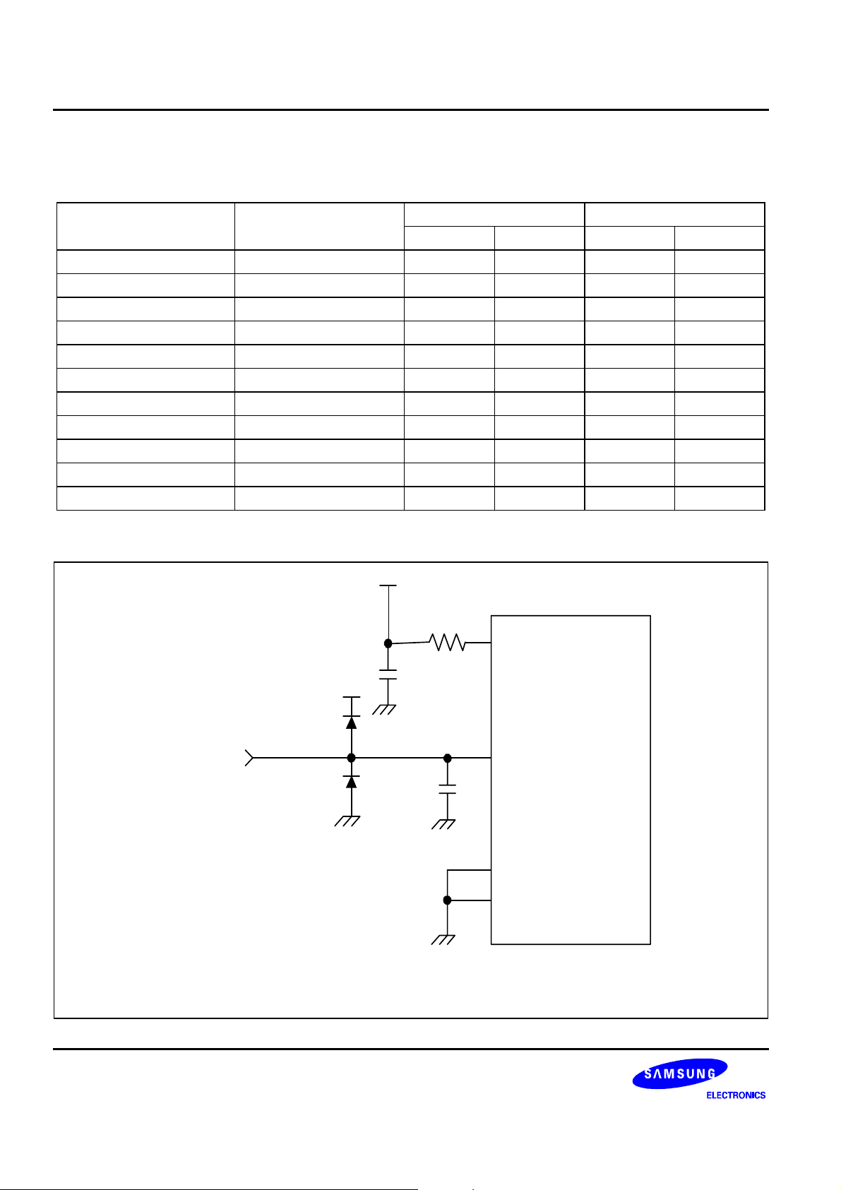
32. ELECTRICAL DATA (PAGE 21-14)
V
DD
V
SS
Test
Reset
S3C84I8X/F84I8X/
C84I9X/F84I9X
Figure 21-9. The Circuit Diagram to Improve EFT Characteristics
NOTE: To improve EFT characteristics, we recommend using capacitor between Vdd and Vss, Test and Vss, Reset and Vss
closely from S3C84I8X/F84I8X/C84I9X/F84I9X. And you’d better also put External crystal closely from
S3C84I8X/F84I8X/C84I9X/F84I9X.
29
Page 35

USER’S MANUAL ERRATA S3C84I8X/F84I8X/C84I9X/F84I9X_ERRATA_REV 2.00
33. CHAPTER 23
OVERVIEW
Samsung provides a powerful and easy-to-use development support system on a turnkey basis. The
development support system is composed of a host system, debugging tools, and supporting software. For a host
system, any standard computer that employs Win95/98/2000/XP as its operating system can be used. A
sophisticated debugging tool is provided both in hardware and software: the powerful in-circuit emulator,
OPENice-i500 and SK-1200, for the S3C7-, S3C9-, and S3C8- microcontroller families. Samsung also offers
supporting software that includes, debugger, an assembler, and a program for setting options.
Target Boards
Target boards are available for all the S3C8/S3F8-series microcontrollers. All the required target system cables
and adapters are included on the device-specific target board. TB84I9/8 is a specific target board for the
development of application systems using S3F84I9X/8X.
programming socket adapter
When you program S3F84I9X/I8X’s flash memory by using an emulator or OTP/MTP writer, you need a specific
programming socket adapter for S3F84I9X/I8X.
30
Page 36

S3C84I8X/F84I8X/C84I9X/F84I9X_ERRATA_REV 2.00 USER’S MANUAL ERRATA
[Development System Configuration]
IBM-PC AT or Compatible
RS-232C / USB
Emulator [ SK-1200(RS-232,USB) or
OPENIce I-500(RS-232) ]
OTP/MTP Writer Block
RAM Break/Display Block
Bus
Trace/Timer Block
SAM8 Base Block
Power Supply Block
POD
Target
Application
System
Probe
Adapter
TB80K9
Target
Board
EVA
Chip
Figure 23-1. Development System Configuration
31
Page 37

USER’S MANUAL ERRATA S3C84I8X/F84I8X/C84I9X/F84I9X_ERRATA_REV 2.00
TB84I9/I8 Target Board
The TB80KB target board can be used for development of S3F80K9X and S3F80KBX together.
But you should be careful to set the memory size to program internal flash memory.
The TB80KB target board is operated as target CPU with Emulator (SK-1200, OPENIce I-500)
In-Circuit Emulator
(SK-1200,OPENIce I-500)
R4
J101
42SDIP
1
5
10
15
21
REV.X
'200X.XX.X
+
C12
44QFP
1
42
40
5
35
10
30
15
25
22
22
X
CC
GND V
J102
44
40
35
30
2520
23
P2
To User_V
OFF ON
Connector
100-Pin
RESET
CN1
100-Pin
Connector
CC
TB84I9/8/84H5
IDLE+STOP
C11
U2
R7
R8
Y1
JP10
C9
C10
30 20 10 1
90 100 110 120
JP1
Y2
+
AR2
C2
C3
CB
C7
160
150
AR1
140
130
C16
SW1
T1T2T3T
R1D1C1
50
60
70
80
4
R5
SMDS2 SMDS2+
Figure 23-2. S3F84I9X/S3F84I8X Target Board Configuration
32
Page 38

S3C84I8X/F84I8X/C84I9X/F84I9X_ERRATA_REV 2.00 USER’S MANUAL ERRATA
Table 23-1. Components of TB84I9/I8
Symbols Usage Description
CN1 100-pin connector Connection between emulator and TB84I9/8 target
board.
J101/J102 50-pin connector Connection between target board and user application
system
RESET Push button Generation low active reset signal to S3F84I9X/8X
EVA-chip
VCC, GND POWER connector External power connector for TB84I9/8
IDLE, STOP LED STOP/IDLE Display Indicate the status of STOP or IDLE of S3F84I9X/8X
EVA-chip on TB8I9/8 target board
Table 23-2. Power Selection Settings for TB84I9
To User_Vcc' Settings Operating Mode Comments
To User_V
Off On
DD
TB84I9
V
DD
V
SS
V
DD
SMDS2+ or SK-1000
To User_V
Off On
DD
V
DD
SMDS2+ or SK-1000
TB84I9
External
DD
V
V
SS
IDLE LED
This LED is ON when the evaluation chip (S3E84I0) is in idle mode.
Target
System
Target
System
SMDS2+ or SK-1000 supplies
to the target board
V
DD
(evaluation chip) and the
target system.
SMDS2+ or SK-1000 supplies
only to the target board
V
DD
(evaluation chip). The target
system must have a power
supply of its own.
STOP LED
This LED is ON when the evaluation chip (S3E84I0) is in stop mode.
33
Page 39

USER’S MANUAL ERRATA S3C84I8X/F84I8X/C84I9X/F84I9X_ERRATA_REV 2.00
ON
OFF
3EH.0 3EH.1 3EH.2 3FH.7
ON
OFF
NOTE: Smart option is determined by DIP switch.
Low
High
Figure 23-3. DIP Switch for Smart Option
Address Switch Function
3EH.1/3EH.0
3EH.1/3EH.0
3EH.1/3EH.0
3EH.1/3EH.0
ON/ON ISP Protection size: 256bytes
ON/OFF ISP Protection size: 512bytes
OFF/ON ISP Protection size: 1024bytes
OFF/OFF ISP Protection size: 2048bytes
ON ISP protection enable
3EH.2
OFF ISP protection disable
ON LVR disable
3FH.7
OFF LVR enable
Table 23-3. Clock Source Selection Setting
Jumper Setting Description
JP10
When to use the external clock from socket(Y2).
JP10
When to use the internal clock from an emulator.
34
Page 40

S3C84I8X/F84I8X/C84I9X/F84I9X_ERRATA_REV 2.00 USER’S MANUAL ERRATA
Table 23-4. PWM Enable/Disable Setting
Jumper Setting Description
JP1
JP1
PWM is disabled during no run.
PWM is always enabled whether run or not.
J102
INT0/TAOUT/P1.0
INT1/BUZ/TACK/P1.1
INT2/TACAP/P1.2
INT3/T1OUT1/P1.3
TBPWM/T1CK0/P2.0
T1CAP0/PWM/P2.1
T1OUT0/AD4/P2.2
AD5/T1CK1/P1.4
T1CAP1/AD6/P1.5
SI/AD7/P2.3
SO/SEG0/P2.4
SCK/SEG1/P2.5
Rx/SEG2/P2.6
TX/SEG3/P2.7
VDD
VSS
X
OUT
X
IN
TEST
Xtin
Xtout
nRESET
10
11
12
13
14
15
16
17
18
19
20
21
22
1
2
3
4
5
6
7
8
9
44-PIN DIP SOCKET
44
43
42
41
40
39
38
37
36
35
34
33
32
31
30
29
28
27
26
25
24
23
P4.7/SEG19/COM7
P4.6/SEG18/COM6
P4.5/SEG17/COM5
P4.4/SEG16/COM4
P4.3/SEG15
P4.2/SEG14
P4.1/SEG13
P4.0/SEG12
P3.7/SEG11
P3.6/SEG10
P3.5/SEG9
P3.4/SEG8
P3.3/SEG7
P3.2/SEG6
P3.1/SEG5
P3.0/SEG4
P0.3/COM3/AD3
P0.2/COM2/AD2
P0.1/COM1/AD1
P0.0/COM0/AD0
Avss
Avref
Figure 23-4. 44-Pin Connector Pin Assignment for TB84I9
35
Page 41

USER’S MANUAL ERRATA S3C84I8X/F84I8X/C84I9X/F84I9X_ERRATA_REV 2.00
J102
SEG14/P4.2
SEG15P4.3
SEG16/COM4/P4.4
SEG17/COM5/P4.5
COM6/SEG18/P4.6
COM7/SEG19/P4.7
INT0/TAOUT/P1.0
INT1/BUZ/TACK/P1.1
INT2/TACAP/P1.2
INT3/T1OUT1/P1.3
VDD
VSS
Xout
Xin
TEST
XTin
XTout
nRESET
TBPWM/T1CK0/P2.0
PWM/T1CAP0/P2.1
T1OUT0/AD4/P2.2
10
11
12
13
14
15
16
17
18
19
20
21
1
2
3
4
5
6
7
8
9
42-PIN DIP SOCKET
42
41
40
39
38
37
36
35
34
33
32
31
30
29
28
27
26
25
24
23
22
P4.1/SEG13
P4.0/SEG12
P3.7/SEG11
P3.6/SEG10
P3.5/SEG9
P3.4/SEG8
P3.3/SEG7
P3.2/SEG6
P3.1/SEG5
P3.0/SEG4
AD3/COM3/P0.3
AD2/COM2/P0.2
AD1/COM1/P0.1
AD0/COM0/P0.0
AVss
AVref
P2.7/SEG3/TxD
P2.6/SEG2/RxD
P2.5/SEG1/SCK
P2.4/SEG0/SO
P2.3/AD7/SI
Figure 23-5. 42-Pin Connector Pin Assignment for TB84I9
Target Board
J101
144
44-Pin Connector
22 23
Part Name: AS20D
Order Cods: SM6304
Target System
144
22 23
44-Pin Connector
Figure 23-6. TB84I9 Adapter Cable for 44pin Connector Package
36
Page 42

S3C84I8X/F84I8X/C84I9X/F84I9X_ERRATA_REV 2.00 USER’S MANUAL ERRATA
Third parties for development tools
SAMSUNG provides a complete line of development tools for SAMSUNG's microcontroller. With long experience
in developing MCU systems, our third parties are leading companies in the tool's technology. SAMSUNG Incircuit emulator solution covers a wide range of capabilities and prices, from a low cost ICE to a complete system
with an OTP/MTP programmer.
In-Circuit Emulator for SAM8 family
— OPENice-i500
— SmartKit SK-1200
OTP/MTP Programmer
— SPW-uni
— AS-pro
— US-pro
— GW-PRO2 (8 - gang programmer)
Development Tools Suppliers
Please contact our local sales offices or the 3rd party tool suppliers directly as shown below for getting
development tools.
8-bit In-Circuit Emulator
OPENice - i500
AIJI System
• TEL: 82-31-223-6611
• FAX: 82-331-223-6613
• E-mail : openice@aijisystem.com
• URL : http://www.aijisystem.com
SK-1200
Seminix
• TEL: 82-2-539-7891
• FAX: 82-2-539-7819
• E-mail: sales@seminix.com
• URL: http://www.seminix.com
37
Page 43

USER’S MANUAL ERRATA S3C84I8X/F84I8X/C84I9X/F84I9X_ERRATA_REV 2.00
OTP/MTP PROGRAMMER (WRITER)
SPW-uni
Single OTP/ MTP/FLASH Programmer
• Download/Upload and data edit function
• PC-based operation with USB port
• Full function regarding OTP/MTP/FLASH MCU
programmer
(Read, Program, Verify, Blank, Protection..)
• Fast programming speed (4Kbyte/sec)
• Support all of SAMSUNG OTP/MTP/FLASH MCU
devices
• Low-cost
• NOR Flash memory (SST,Samsung…)
• NAND Flash memory (SLC)
• New devices will be supported just by adding
device files or upgrading the software.
AS-pro
On-board programmer for Samsung Flash MCU
• Portable & Stand alone Samsung
OTP/MTP/FLASH Programmer for After Service
• Small size and Light for the portable use
• Support all of SAMSUNG OTP/MTP/FLASH
devices
• HEX file download via USB port from PC
• Very fast program and verify time
( OTP:2Kbytes per second, MTP:10Kbytes per
second)
• Internal large buffer memory (118M Bytes)
• Driver software run under various O/S
(Windows 95/98/2000/XP)
• Full function regarding OTP/MTP programmer
(Read, Program, Verify, Blank, Protection..)
• Two kind of Power Supplies
(User system power or USB power adapter)
• Support Firmware upgrade
SEMINIX
• TEL: 82-2-539-7891
• FAX: 82-2-539-7819.
• E-mail:
sales@seminix.com
• URL:
http://www.seminix.com
SEMINIX
• TEL: 82-2-539-7891
• FAX: 82-2-539-7819.
• E-mail:
sales@seminix.com
• URL:
http://www.seminix.com
38
Page 44

S3C84I8X/F84I8X/C84I9X/F84I9X_ERRATA_REV 2.00 USER’S MANUAL ERRATA
US-pro
Portable Samsung OTP/MTP/FLASH Programmer
• Portable Samsung OTP/MTP/FLASH Programmer
• Small size and Light for the portable use
• Support all of SAMSUNG OTP/MTP/FLASH
devices
• Convenient USB connection to any IBM compatible
PC or Laptop computers.
• Operated by USB power of PC
• PC-based menu-drive software for simple operation
• Very fast program and verify time
( OTP:2Kbytes per second, MTP:10Kbytes per
second)
• Support Samsung standard Hex or Intel Hex format
• Driver software run under various O/S
(Windows 95/98/2000/XP)
• Full function regarding OTP/MTP programmer
(Read, Program, Verify, Blank, Protection..)
• Support Firmware upgrade
SEMINIX
• TEL: 82-2-539-7891
• FAX: 82-2-539-7819.
• E-mail:
sales@seminix.com
• URL:
http://www.seminix.com
GW-PRO2
Gang Programmer for OTP/MTP/FLASH MCU
• 8 devices programming at one time
• Fast programming speed (1.2Kbyte/sec)
• PC-based control operation mode or Stand-alone
• Full Function regarding OTP/MTP program
(Read, Program, Verify, Protection, Blank..)
• Data back-up even at power break
After setup in Design Lab, it can be moved to the
factory site.
• Key Lock protecting operator's mistake
• Good/Fail quantity displayed and memorized
• Buzzer sounds after programming
• User friendly single-menu operation (PC)
• Operation status displayed in LCD panel
SEMINIX
• TEL: 82-2-539-7891
• FAX: 82-2-539-7819.
• E-mail:
sales@seminix.com
• URL:
http://www.seminix.com
39
Page 45

Preface
The S3C84I8X/F84I8X/C84I9X/F84I9X Microcontroller User's Manual is designed for application designers and
programmers who are using the S3C84I8X/F84I8X/C84I9X/F84I9X microcontroller for application development. It
is organized in two main parts:
Part I Programming Model Part II Hardware Descriptions
Part I contains software-related information to familiarize you with the microcontroller's architecture, programming
model, instruction set, and interrupt structure. It has six chapters:
Chapter 1 Product Overview
Chapter 2 Address Spaces
Chapter 3 Addressing Modes
Chapter 1, "Product Overview," is a high-level introduction to S3C84I8X/F84I8X/C84I9X/F84I9X with general
product descriptions, as well as detailed information about individual pin characteristics and pin circuit types.
Chapter 2, "Address Spaces," describes program and data memory spaces, the internal register file, and register
addressing. Chapter 2 also describes working register addressing, as well as system stack and user-defined
stack operations.
Chapter 3, "Addressing Modes," contains detailed descriptions of the addressing modes that are supported by the
S3C8-series CPU.
Chapter 4, "Control Registers," contains overview tables for all mapped system and peripheral control register
values, as well as detailed one-page descriptions in a standardized format. You can use these easy-to-read,
alphabetically organized, register descriptions as a quick-reference source when writing programs.
Chapter 5, "Interrupt Structure," describes the S3C84I8X/F84I8X/C84I9X/F84I9X interrupt structure in detail and
further prepares you for additional information presented in the individual hardware module descriptions in Part II.
Chapter 6, "Instruction Set," describes the features and conventions of the instruction set used for all S3C8-series
microcontrollers. Several summary tables are presented for orientation and reference. Detailed descriptions of
each instruction are presented in a standard format. Each instruction description includes one or more practical
examples of how to use the instruction when writing an application program.
A basic familiarity with the information in Part I will help you to understand the hardware module descriptions in
Part II. If you are not yet familiar with the S3C8-series microcontroller family and are reading this manual for the
first time, we recommend that you first read Chapters 1–3 carefully. Then, briefly look over the detailed
information in Chapters 4, 5, and 6. Later, you can reference the information in Part I as necessary.
Chapter 4 Control Registers
Chapter 5 Interrupt Structure
Chapter 6 Instruction Set
Part II "hardware Descriptions," has detailed information about specific hardware components of the
S3C84I8X/F84I8X/C84I9X/F84I9X microcontroller. Also included in Part II are electrical, mechanical, OTP, and
development tools data. It has 17 chapters:
Chapter 7 Clock Circuit
Chapter 8 RESET and Power-Down
Chapter 9 I/O Ports
Chapter 10 Basic Timer
Chapter 11 8-bit Timer A/B
Chapter 12 16-bit Timer 1(0,1)
Chapter 13 10-bit PWM
(pulse width modulation)
Chapter 14 Serial I/O Interface
Chapter 15 UART
S3C84I8X/F84I8X/C84I9X/F84I9X_USER’S MANUAL_REV 2.00 MICROCONTROLLER iii
Chapter 16 A/D Converter
Chapter 17 Watch Timer
Chapter 18 LCD Controller/Driver
Chapter 19 Low Voltage RESET
Chapter 20 Embedded Flash Memory
Interface
Chapter 21 Electrical Data
Chapter 22 Mechanical Data
Chapter 23 Development Tools
Page 46

Table of Contents
Part I — Programming Model
Chapter 1 Product Overview
S3C8-Series Microcontrollers........................................................................................................................1-1
S3C84I8X/F84I8X/C84I9X/F84I9X Microcontroller........................................................................................1-1
Features.........................................................................................................................................................1-2
Block Diagram................................................................................................................................................1-3
Pin Assignment..............................................................................................................................................1-4
Pin Assignment..............................................................................................................................................1-5
Pin Descriptions.............................................................................................................................................1-6
Pin Circuits.....................................................................................................................................................1-9
Chapter 2 Address Spaces
Overview ........................................................................................................................................................2-1
Program Memory (ROM) ...............................................................................................................................2-2
Register Architecture .....................................................................................................................................2-4
Register Page Pointer (PP)..................................................................................................................2-7
Register Set 1.......................................................................................................................................2-9
Register Set 2.......................................................................................................................................2-9
Prime Register Space...........................................................................................................................2-10
Working Registers ................................................................................................................................2-12
Using The Register Pointers.................................................................................................................2-13
Register Addressing.......................................................................................................................................2-15
Common Working Register AREA (C0H–CFH) ...................................................................................2-17
4-Bit Working Register Addressing ......................................................................................................2-18
8-Bit Working Register Addressing ......................................................................................................2-20
System and User Stack .................................................................................................................................2-22
Chapter 3 Addressing Modes
Overview ........................................................................................................................................................3-1
Register Addressing Mode (R).......................................................................................................................3-2
Indirect Register Addressing Mode (IR).........................................................................................................3-3
Indexed Addressing Mode (X) .......................................................................................................................3-7
Direct Address Mode (DA).............................................................................................................................3-10
Indirect Address Mode (IA)............................................................................................................................3-12
Relative Address Mode (RA) .........................................................................................................................3-13
Immediate Mode (IM).....................................................................................................................................3-14
S3C84I8X/F84I8X/C84I9X/F84I9X_USER’S MANUAL_REV 2.00 MICROCONTROLLER v
Page 47

Table of Contents (Continued)
Chapter 4 Control Registers
Overview....................................................................................................................................................... 4-1
Chapter 5 Interrupt Structure
Overview........................................................................................................................................................ 5-1
Interrupt Types..................................................................................................................................... 5-2
S3C84I8X/F84I8X/C84I9X/F84I9X Interrupt Structure........................................................................ 5-4
Interrupt Vector Addresses.................................................................................................................. 5-6
Enable/Disable Interrupt Instructions (EI, DI) ...................................................................................... 5-8
System-Level Interrupt Control Registers............................................................................................ 5-8
Interrupt Processing Control Points..................................................................................................... 5-9
Peripheral Interrupt Control Registers................................................................................................. 5-10
System Mode Register (SYM) ............................................................................................................. 5-11
Interrupt Mask Register (IMR) ............................................................................................................. 5-12
Interrupt Priority Register (IPR)............................................................................................................ 5-13
Interrupt Request Register (IRQ)......................................................................................................... 5-15
Interrupt Pending Function Types........................................................................................................ 5-16
Interrupt Source Polling Sequence...................................................................................................... 5-17
Interrupt Service Routines ................................................................................................................... 5-17
Generating interrupt Vector Addresses ............................................................................................... 5-18
Nesting of Vectored Interrupts............................................................................................................. 5-18
Chapter 6 Instruction Set
Overview....................................................................................................................................................... 6-1
Data Types........................................................................................................................................... 6-1
Register Addressing............................................................................................................................. 6-1
Addressing Modes............................................................................................................................... 6-1
Flags Register (FLAGS)....................................................................................................................... 6-6
Flag Descriptions ................................................................................................................................. 6-7
Instruction Set Notation........................................................................................................................ 6-8
Condition Codes .................................................................................................................................. 6-12
Instruction Descriptions........................................................................................................................ 6-13
vi S3C84I8X/F84I8X/C84I9X/F84I9X_USER’S MANUAL_REV 2.00 MICROCONTROLLER
Page 48

Table of Contents (Continued)
Part II Hardware Descriptions
Chapter 7 Clock Circuit
Overview ........................................................................................................................................................7-1
System Clock Circuit ............................................................................................................................7-1
Clock Status During Power-Down Modes............................................................................................7-2
System Clock Control Register (CLKCON)..........................................................................................7-3
Chapter 8 RESET and Power-Down
System Reset.................................................................................................................................................8-1
Overview...............................................................................................................................................8-1
Normal Mode Reset Operation.............................................................................................................8-1
Hardware Reset Values........................................................................................................................8-2
Power-Down Modes.......................................................................................................................................8-5
Stop Mode ............................................................................................................................................8-5
Idle Mode..............................................................................................................................................8-6
Chapter 9 I/O Ports
Overview ........................................................................................................................................................9-1
Port Data Registers ..............................................................................................................................9-2
Port 0 ....................................................................................................................................................9-3
Port 1 ....................................................................................................................................................9-6
Port 2 ....................................................................................................................................................9-9
Port 3 ....................................................................................................................................................9-14
Port 4 ....................................................................................................................................................9-17
Chapter 10 Basic Timer
Overview ........................................................................................................................................................10-1
Basic Timer (BT)...................................................................................................................................10-1
Basic Timer Control Register (BTCON) ...............................................................................................10-1
Basic Timer Function Description.........................................................................................................10-3
S3C84I8X/F84I8X/C84I9X/F84I9X_USER’S MANUAL_REV 2.00 MICROCONTROLLER vii
Page 49

Table of Contents (Continued)
Chapter 11 8-Bit Timer A/B
8-Bit Timer A.................................................................................................................................................. 11-1
Overview.............................................................................................................................................. 11-1
Function Description............................................................................................................................11-2
Timer A Control Register (TACON)..................................................................................................... 11-3
Block Diagram...................................................................................................................................... 11-4
8-Bit Timer B.................................................................................................................................................. 11-5
Overview.............................................................................................................................................. 11-5
Block Diagram...................................................................................................................................... 11-5
Timer B Control Register (TBCON)..................................................................................................... 11-6
Timer B Pulse Width Calculations ....................................................................................................... 11-7
Chapter 12 16-Bit Timer 1(0, 1)
Overview........................................................................................................................................................ 12-1
Function Description............................................................................................................................12-2
Timer 1(0,1) Control Register (T1CON0, T1CON1)............................................................................ 12-3
Block Diagram...................................................................................................................................... 12-6
Chapter 13 10-bit PWM (Pulse width Modulation)
Overview........................................................................................................................................................ 13-1
Function Description...................................................................................................................................... 13-1
PWM .................................................................................................................................................... 13-1
PWM Control Register (PWMCON)..................................................................................................... 13-5
Chapter 14 Serial I/O Interface
Overview........................................................................................................................................................ 14-1
Programming Procedure...................................................................................................................... 14-1
Serial I/O Control Registers (SIOCON) ............................................................................................... 14-2
SIO Prescaler Register (SIOPS).......................................................................................................... 14-3
viii S3C84I8X/F84I8X/C84I9X/F84I9X_USER’S MANUAL_REV 2.00 MICROCONTROLLER
Page 50

Table of Contents (Continued)
Chapter 15 UART
Overview ........................................................................................................................................................15-1
Programming Procedure ......................................................................................................................15-1
Uart Control Register (UARTCON) ......................................................................................................15-2
Uart Interrupt Pending Register (UARTPND).......................................................................................15-4
Uart Data Register (UDATA)................................................................................................................15-5
Uart Baud Rate Data Register (BRDATAH, BRDATAL)......................................................................15-6
Baud Rate Calculations........................................................................................................................15-6
Block Diagram................................................................................................................................................15-8
Uart Mode 0 Function Description........................................................................................................15-9
Uart Mode 1 Function Description........................................................................................................15-10
Uart Mode 2 Function Description........................................................................................................15-11
Serial Communication for Multiprocessor Configurations....................................................................15-13
Chapter 16 A/D Converter
Overview ........................................................................................................................................................16-1
Function Description ......................................................................................................................................16-1
A/D Converter Control Register (ADCON)...........................................................................................16-2
Internal Reference Voltage Levels .......................................................................................................16-4
Conversion timing.................................................................................................................................16-4
Internal A/D Conversion Procedure......................................................................................................16-5
Chapter 17 Watch Timer
Overview ........................................................................................................................................................17-1
Watch Timer Control Register (WTCON: R/W)....................................................................................17-2
Watch Timer Circuit Diagram ...............................................................................................................17-3
Chapter 18 LCD Controller/Driver
Overview ........................................................................................................................................................18-1
LCD Circuit Diagram.............................................................................................................................18-2
LCD RAM Address Area.......................................................................................................................18-3
LCD Mode Control Register (LMOD) ...................................................................................................18-4
LCD Port Control Register....................................................................................................................18-5
LCD Voltage Dividing Resistors ...........................................................................................................18-6
Common (COM) Signals ......................................................................................................................18-6
Segment (SEG) Signals .......................................................................................................................18-6
Chapter 19 Low Voltage Reset
Overview........................................................................................................................................................19-1
S3C84I8X/F84I8X/C84I9X/F84I9X_USER’S MANUAL_REV 2.00 MICROCONTROLLER ix
Page 51

Table of Contents (Continued)
Chapter 20 Embedded Flash Memory Interface
Overview........................................................................................................................................................ 20-1
Flash Memory Control Registers................................................................................................................... 20-3
Sector Erase.................................................................................................................................................. 20-5
Programming................................................................................................................................................. 20-8
Reading......................................................................................................................................................... 20-11
Hard Lock Protection..................................................................................................................................... 20-12
Chapter 21 Electrical Data
Overview....................................................................................................................................................... 21-1
Chapter 22 Mechanical Data
Overview....................................................................................................................................................... 22-1
Chapter 23 Development Tools
Overview........................................................................................................................................................ 23-1
Target Boards ...................................................................................................................................... 23-1
Programming Socket Adapter.............................................................................................................. 23-1
IDLE LED............................................................................................................................................. 23-4
STOP LED ........................................................................................................................................... 23-4
OTP/MTP Programmer (Writer)........................................................................................................... 23-9
x S3C84I8X/F84I8X/C84I9X/F84I9X_USER’S MANUAL_REV 2.00 MICROCONTROLLER
Page 52

List of Figures
Figure Title Page
Number Number
1-1 S3C84I8X/F84I8X/C84I9X/F84I9X Block Diagram ....................................................1-3
1-2 S3C84I8X/F84I8X/C84I9X/F84I9X Pin Assignment (44-pin QFP).............................1-4
1-3 S3C84I9X/F84I9X Pin Assignment (42-pin SDIP) .....................................................1-5
1-4 Pin Circuit Type B (nRESET) .....................................................................................1-9
1-5 Pin Circuit Type C.......................................................................................................1-9
1-6 Pin Circuit Type D.......................................................................................................1-10
1-7 Pin Circuit Type D-5 (P1.0–P1.3)...............................................................................1-10
1-8 Pin Circuit Type E (P2.2–P2.3)...................................................................................1-11
1-9 Pin Circuit Type H-4 ...................................................................................................1-12
1-10 Pin Circuit Type H-14 (P4.4–P4.7).............................................................................1-13
1-11 Pin Circuit Type H-16 (P0.0–P0.3).............................................................................1-13
1-12 Pin Circuit Type H-17 (2.4–P2.7, P3.0–P3.7, P4.0–P4.3)..........................................1-14
2-1 Program Memory Address Space ..............................................................................2-2
2-2 Smart Option...............................................................................................................2-3
2-3 Internal Register File Organization of S3F84I9X/C84I9X...........................................2-5
2-4 Internal Register File Organization of S3F84I8X/C84I8X...........................................2-6
2-5 Register Page Pointer (PP)........................................................................................2-7
2-6 Set 1, Set 2, Prime Area Register(S3C84I9X/F84I9X)...............................................2-10
2-7 Set 1, Set 2, Prime Area Register (S3C84I8X/F84I8X)..............................................2-11
2-8 8-Byte Working Register Areas (Slices).....................................................................2-12
2-9 Contiguous 16-Byte Working Register Block .............................................................2-13
2-10 Non-Contiguous 16-Byte Working Register Block .....................................................2-14
2-11 16-Bit Register Pair ....................................................................................................2-15
2-12 Register File Addressing ............................................................................................2-16
2-13 Common Working Register Area................................................................................2-17
2-14 4-Bit Working Register Addressing ............................................................................2-19
2-15 4-Bit Working Register Addressing Example .............................................................2-19
2-16 8-Bit Working Register Addressing ............................................................................2-20
2-17 8-Bit Working Register Addressing Example .............................................................2-21
2-18 Stack Operations........................................................................................................2-22
3-1 Register Addressing ...................................................................................................3-2
3-2 Working Register Addressing.....................................................................................3-2
3-3 Indirect Register Addressing to Register File.............................................................3-3
3-4 Indirect Register Addressing to Program Memory.....................................................3-4
3-5 Indirect Working Register Addressing to Register File ..............................................3-5
3-6 Indirect Working Register Addressing to Program or Data Memory..........................3-6
3-7 Indexed Addressing to Register File ..........................................................................3-7
3-8 Indexed Addressing to Program or Data Memory with Short Offset..........................3-8
3-9 Indexed Addressing to Program or Data Memory......................................................3-9
3-10 Direct Addressing for Load Instructions .....................................................................3-10
3-11 Direct Addressing for Call and Jump Instructions......................................................3-11
3-12 Indirect Addressing.....................................................................................................3-12
3-13 Relative Addressing....................................................................................................3-13
3-14 Immediate Addressing................................................................................................3-14
S3C84I8X/F84I8X/C84I9X/F84I9X_USER’S MANUAL_REV 2.00 MICROCONTROLLER xi
Page 53

List of Figures (Continued)
Figure Title Page
Number Number
4-1 Register Description Format...................................................................................... 4-4
5-1 S3C8-Series Interrupt Types ..................................................................................... 5-3
5-2 S3C84I8X/F84I8X/C84I9X/F84I9XInterrupt Structure............................................... 5-5
5-3 ROM Vector Address Area ........................................................................................ 5-6
5-4 Interrupt Function Diagram........................................................................................ 5-9
5-5 System Mode Register (SYM) ................................................................................... 5-11
5-6 Interrupt Mask Register (IMR) ...................................................................................5-12
5-7 Interrupt Request Priority Groups.............................................................................. 5-13
5-8 Interrupt Priority Register (IPR) ................................................................................. 5-14
5-9 Interrupt Request Register (IRQ)............................................................................... 5-15
6-1 System Flags Register (FLAGS) ............................................................................... 6-6
7-1 Main Oscillator Circuit (Crystal or Ceramic Oscillator) .............................................. 7-1
7-2 Sub-System Oscillator Circuit (Crystal Oscillator) ..................................................... 7-1
7-3 System Clock Circuit Diagram................................................................................... 7-2
7-4 System Clock Control Register (CLKCON) ............................................................... 7-3
7-5 Oscillator Control Register (OSCCON) ..................................................................... 7-4
7-6 STOP Control Register (STOPCON)......................................................................... 7-4
9-1 Port 0 Low Byte Control Register (P0CON) .............................................................. 9-4
9-2 Port 1 High-Byte Control Register (P1CONH)........................................................... 9-7
9-3 Port 1 Low-Byte Control Register (P1CONL) ............................................................ 9-7
9-4 Port 1 Interrupt Pending Register (P1INTPND)......................................................... 9-8
9-5 Port 1 Interrupt Enable Register (P1INT) .................................................................. 9-9
9-6 Port 2 High-Byte Control Register (P2CONH)........................................................... 9-10
9-7 Port 2 Low-Byte Control Register (P2CONL) ............................................................ 9-11
9-8 Port 2 Pull-up Control Register (P2PUR) .................................................................. 9-12
9-9 Port 3 High-Byte Control Register (P3CONH)........................................................... 9-14
9-10 Port 3 Low-Byte Control Register (P3CONL)............................................................ 9-15
9-11 Port 4 High-Byte Control Register (P4CONH)........................................................... 9-17
9-12 Port 4 Low-Byte Control Register (P4CONL)............................................................ 9-18
10-1 Basic Timer Control Register (BTCON)..................................................................... 10-2
10-2 Basic Timer Block Diagram .......................................................................................10-4
11-1 Timer A Control Register (TACON)........................................................................... 11-3
11-2 Timer A Functional Block Diagram............................................................................ 11-4
11-3 Timer B Functional Block Diagram............................................................................ 11-5
11-4 Timer B Control Register (TBCON)........................................................................... 11-6
11-5 Timer B Data Registers (TBDATAH, TBDATAL)....................................................... 11-6
11-6 Timer B Output Flip Flop Waveforms in Repeat Mode.............................................. 11-8
xii S3C84I8X/F84I8X/C84I9X/F84I9X_USER’S MANUAL_REV 2.00 MICROCONTROLLER
Page 54

List of Figures (Concluded)
Figure Title Page
Number Number
12-1 Timer 1(0,1) Control Register (T1CON0, T1CON1)...................................................12-4
12-2 Timer A, Timer 1(0,1) Pending Register (TINTPND) .................................................12-5
12-3 Timer 1(0,1) Functional Block Diagram......................................................................12-6
13-1 10-Bit PWM Basic Waveform.....................................................................................13-3
13-2 10-Bit Extended PWM Waveform...............................................................................13-4
13-3 PWM Control Register (PWMCON) ...........................................................................13-5
13-4 PWM Functional Block Diagram.................................................................................13-6
14-1 Serial I/O Interface Control Register (SIOCON).........................................................14-2
14-2 SIO Pre-Scaler Register (SIOPS) ..............................................................................14-3
14-3 SIO Functional Block Diagram ...................................................................................14-3
14-4 Serial I/O Timing in Transmit-Receive Mode (Tx at falling, SIOCON.4 = 0)..............14-4
14-5 Serial I/O Timing in Transmit-Receive Mode (Tx at rising, SIOCON.4 = 1)...............14-4
14-6 Serial I/O Timing in Receive-Only Mode....................................................................14-5
15-1 UART Control Register (UARTCON) .........................................................................15-3
15-2 UART Interrupt Pending Register (UARTPND)..........................................................15-4
15-3 UART Data Register (UDATA)...................................................................................15-5
15-4 UART Baud Rate Data Register (BRDATAH, BRDATAL).........................................15-6
15-5 UART Functional Block Diagram................................................................................15-8
15-6 Timing Diagram for UART Mode 0 Operation............................................................15-9
15-7 Timing Diagram for UART Mode 1 Operation............................................................15-10
15-8 Timing Diagram for UART Mode 2 Operation............................................................15-12
15-9 Connection Example for Multiprocessor Serial Data Communications .....................15-14
16-1 A/D Converter Control Register (ADCON).................................................................16-2
16-2 A/D Converter Data Register (ADDATAH, ADDATAL)..............................................16-3
16-3 A/D Converter Circuit Diagram...................................................................................16-3
16-4 A/D Converter Timing Diagram ..................................................................................16-4
16-5 Recommended A/D Converter Circuit for Highest Absolute Accuracy ......................16-5
17-1 Watch Timer Circuit Diagram .....................................................................................17-3
18-1 LCD Function Diagram...............................................................................................18-1
18-2 LCD Circuit Diagram...................................................................................................18-2
18-3 LCD Display Data RAM Organization ........................................................................18-3
18-4 LCD Mode Control Register (LMOD) .........................................................................18-4
18-5 LCD Port Control Register..........................................................................................18-5
18-6 Internal Voltage Dividing Resistor Connection...........................................................18-6
18-7 LCD Signal Waveforms (1/8 Duty, 1/4 Bias)..............................................................18-7
18-8 LCD Signal Waveforms (1/4 Duty, 1/3 Bias)..............................................................18-8
18-9 LCD Signal Waveforms (1/3 Duty, 1/3 Bias)..............................................................18-9
19-1 Low Voltage Reset Circuit..........................................................................................19-2
S3C84I8X/F84I8X/C84I9X/F84I9X_USER’S MANUAL_REV 2.00 MICROCONTROLLER xiii
Page 55

List of Figures (Concluded)
Figure Title Page
Number Number
20-1 Flash Memory Control Register (FMCON)................................................................ 20-3
20-2 Flash Memory User Programming Enable Register (FMUSR).................................. 20-4
20-3 Sectors in User Program Mode ................................................................................. 20-5
20-4 Flash Memory Sector Address Register (FMSECH)................................................. 20-6
20-5 Flash Memory Sector Address Register (FMSECL).................................................. 20-6
21-1 Input Timing for External Interrupts (Ports 2) ............................................................ 21-6
21-2 Input Timing for nRESET........................................................................................... 21-6
21-3 Clock Timing Measurement at X
21-4 Stop Mode Release Timing initiated by RESET........................................................ 21-9
21-5 Stop Mode (Main) Release Timing Initiated by Interrupts ......................................... 21-10
21-6 Stop Mode (Sub) Release Timing Initiated by Interrupts........................................... 21-10
21-7 Waveform for UART Timing Characteristics.............................................................. 21-11
21-8 Operating Voltage Range .......................................................................................... 21-13
21-9 The Circuit Diagram to Improve EFT Characteristics................................................ 21-14
22-1 42-SDIP-600 Package Dimensions........................................................................... 22-1
22-2 44-QFP-1010 Package Dimensions.......................................................................... 22-2
23-1 Development System Configuration .......................................................................... 23-2
23-2 S3F84I9X/S3F84I8X Target Board Configuration ..................................................... 23-3
23-3 DIP Switch for Smart Option...................................................................................... 23-5
23-4 44-Pin Connector Pin Assignment for TB84I9........................................................... 23-6
23-5 42-Pin Connector Pin Assignment for TB84I9........................................................... 23-7
23-6 TB84I9 Adapter Cable for 44pin Connector Package ............................................... 23-7
............................................................................. 21-8
IN
xiv S3C84I8X/F84I8X/C84I9X/F84I9X_USER’S MANUAL_REV 2.00 MICROCONTROLLER
Page 56

List of Tables
Table Title Page
Number Number
1-1 S3C84I8X/F84I8X/C84I9X/F84I9X Pin Descriptions..................................................1-6
2-1 S3C84I9X/F84I9X Register Type Summary...............................................................2-4
2-2 S3C84I8X/F84I8X Register Type Summary...............................................................2-4
4-1 Set 1 Registers...........................................................................................................4-1
4-2 Set 1, Bank 0 Registers..............................................................................................4-2
4-3 Set 1, Bank 1 Registers..............................................................................................4-3
5-1 Interrupt Vectors.........................................................................................................5-7
5-2 Interrupt Control Register Overview...........................................................................5-8
5-3 Interrupt Source Control and Data Registers.............................................................5-10
6-1 Instruction Group Summary........................................................................................6-2
6-2 Flag Notation Conventions.........................................................................................6-8
6-3 Instruction Set Symbols..............................................................................................6-8
6-4 Instruction Notation Conventions ...............................................................................6-9
6-5 OPCODE Quick Reference........................................................................................6-10
6-6 Condition Codes.........................................................................................................6-12
8-1 S3C84I8X/F84I8X/84I9X/F84I9X Set 1 Register Values After RESET......................8-2
8-2 S3C84I8X/F84I8X/84I9X/F84I9X Set 1, Bank 0 Register Values After RESET ........8-3
8-3 S3C84I8X/F84I8X/84I9X/F84I9X Set 1, Bank 1 Register Values After RESET ........8-4
9-1 S3C84I8X/F84I8X/84I9X/F84I9X Port Configuration Overview.................................9-1
9-2 Port Data Register Summary......................................................................................9-2
13-1 PWM Control and Data Registers..............................................................................13-2
13-2 PWM Output "stretch" Values for Extension Data Register (PWMDATAL .1–.0)......13-3
15-1 Commonly Used Baud Rates Generated by 16bit BRDATA .....................................15-7
17-1 Watch Timer Control Register (WTCON): Set 1, Bank 1, F8H, R/W.........................17-2
18-1 Common and Segment Pins per Duty Cycle..............................................................18-3
S3C84I8X/F84I8X/C84I9X/F84I9X_USER’S MANUAL_REV 2.00 MICROCONTROLLER xv
Page 57

List of Tables
Table Title Page
Number Number
20-1 Descriptions of Pins Used to Read/Write the Flash ROM......................................... 20-1
20-2 Comparison of S3F84I8X/F84I9X and S3C84I8X/C84I9X Features......................... 20-2
21-1 Absolute Maximum Ratings....................................................................................... 21-2
21-2 Input/Output Capacitance.......................................................................................... 21-2
21-3 D.C. Electrical Characteristics ................................................................................... 21-3
21-4 A.C. Electrical Characteristics ...................................................................................21-6
21-5 Main Oscillator Frequency (f
21-6 Main Oscillator Clock Stabilization Time (t
21-7 Sub Oscillator Frequency (f
21-8 Subsystem Oscillator (crystal) Stabilization Time (t
)............................................................................. 21-7
OSC1
).......................................................... 21-7
ST1
).............................................................................. 21-8
OSC2
)............................................ 21-8
ST2
21-9 Data Retention Supply Voltage in Stop Mode ........................................................... 21-9
21-10 UART Timing Characteristics in Mode 0 (10 MHz).................................................... 21-11
21-11 A/D Converter Electrical Characteristics ................................................................... 21-12
21-12 LVR(Low Voltage Reset) Circuit Characteristics .................................................... 21-13
23-1 Components of TB84I9/I8.......................................................................................... 23-4
23-2 Power Selection Settings for TB84I9......................................................................... 23-4
23-3 Clock Source Selection Setting ................................................................................. 23-5
23-4 PWM Enable/Disable Setting..................................................................................... 23-6
xvi S3C84I8X/F84I8X/C84I9X/F84I9X_USER’S MANUAL_REV 2.00 MICROCONTROLLER
Page 58

List of Programming Tips
Description Page
Number
Chapter 2: Address Spaces
Using the Page Pointer for RAM Clear (Page 0, Page 1).............................................................................2-8
Addressing the Common Working Register Area.........................................................................................2-18
Standard Stack Operations Using PUSH and POP......................................................................................2-23
Chapter 11: 8-bit Timer A/B
To Generate 38 kHz, 1/3duty Signal Through P2.0......................................................................................11-9
To Generate a One Pulse Signal Through P2.0...........................................................................................11-10
Using the Timer A..........................................................................................................................................11-11
Using the Timer B..........................................................................................................................................11-12
Chapter 12: 16-bit Timer 1(0,1)
Using the Timer 1(0)......................................................................................................................................12-7
Chapter 13: 10-Bit PWM (Pulse Width Modulation)
Programming the PWM Module to Sample Specifications ...........................................................................13-7
Chapter 14: Serial I/O Interface
SIO ................................................................................................................................................................14-5
Chapter 16: A/D Converter
Configuring A/D Converter............................................................................................................................16-6
Chapter 17: Watch Timer
Using the Watch Timer..................................................................................................................................17-4
Chapter 20: Embedded Flash Memory Interface
Sector Erase (Not to use an interrupt) ..........................................................................................................20-7
Sector Erase (To use an interrupt)................................................................................................................20-7
Programming.................................................................................................................................................20-9
Reading.........................................................................................................................................................20-11
Hard Lock Protection.....................................................................................................................................20-12
S3C84I8X/F84I8X/C84I9X/F84I9X_USER’S MANUAL_REV 2.00 MICROCONTROLLER xvii
Page 59

List of Register Descriptions
Register Full Register Name Page
Identifier Number
ADCON A/D Converter Control Register .................................................................................4-5
BTCON Basic Timer Control Register.....................................................................................4-6
CLKCON System Clock Control Register..................................................................................4-7
FMCON Flash Memory Control Register.................................................................................4-8
FMSECH Flash Memory Sector Register (High byte)................................................................4-9
FMSECL Flash Memory Sector Register (Low byte).................................................................4-9
FMUSR Flash Memory User Programming Enable Register ..................................................4-10
FLAGS System Flags Register...............................................................................................4-11
IMR Interrupt Mask Register..............................................................................................4-12
IPL Instruction Pointer (Low Byte)....................................................................................4-13
IPR Interrupt Priority Register ...........................................................................................4-14
IRQ Interrupt Request Register.........................................................................................4-15
LMOD LCD Mode Control Register.......................................................................................4-16
LPOT LCD Port Control Register .........................................................................................4-17
OSCCON Oscillator Control Register.........................................................................................4-18
P0CON Port 0 Control Register (High Byte)............................................................................4-19
P1CONH Port 1 Control Register (High Byte)............................................................................4-20
P1CONL Port 1 Control Register (Low Byte) ............................................................................4-21
P1INTPND Port 1 Interrupt Pending Register...............................................................................4-22
P1INT Port 1 Interrupt Enable...............................................................................................4-23
P2CONH Port 2 Control Register (High Byte)............................................................................4-24
P2CONL Port 2 Control Register (Low Byte) ............................................................................4-25
P2PUR Port 2 Pull-up Resistor Control Register....................................................................4-26
P3CONH Port 3 Control Register (High Byte)............................................................................4-27
P3CONL Port 3 Control Register (Low Byte) ............................................................................4-28
P4CONH Port 4 Control Register (High Byte)............................................................................4-29
P4CONL Port 4 Control Register (Low Byte) ............................................................................4-30
PP Register Page Pointer................................................................................................4-31
PWMCON PWM Control Register................................................................................................4-32
RP0 Register Pointer 0.......................................................................................................4-33
RP1 Register Pointer 1.......................................................................................................4-33
SIOCON Serial I/O Module Control Registers...........................................................................4-34
SIOPS SIO Prescaler Register ..............................................................................................4-35
SPH Stack Pointer (High Byte)...........................................................................................4-35
SPL Stack Pointer (Low Byte)............................................................................................4-35
STOPCON Stop Control Register.................................................................................................4-36
SYM System Mode Register...............................................................................................4-37
T1CON0 Timer 1(0) Control Register........................................................................................4-38
T1CON1 Timer 1(1) Control Register........................................................................................4-39
TACON Timer A Control Register............................................................................................4-40
TBCON Timer B Control Register............................................................................................4-41
TINTPND Timer A, Timer 1 Interrupt Pending Register.............................................................4-42
UARTCON UART Control Register .............................................................................................4-43
UARTPND UART Pending and Parity Control .............................................................................4-45
WTCON Watch Timer Control Register....................................................................................4-46
S3C84I8X/F84I8X/C84I9X/F84I9X_USER’S MANUAL_REV 2.00 MICROCONTROLLER xix
Page 60

List of Instruction Descriptions
Instruction Full Register Name Page
Mnemonic Number
ADC Add with Carry............................................................................................................6-14
ADD Add.............................................................................................................................6-15
AND Logical AND ...............................................................................................................6-16
BAND Bit AND.......................................................................................................................6-17
BCP Bit Compare ...............................................................................................................6-18
BITC Bit Complement..........................................................................................................6-19
BITR Bit Reset.....................................................................................................................6-20
BITS Bit Set.........................................................................................................................6-21
BOR Bit OR.........................................................................................................................6-22
BTJRF Bit Test, Jump Relative on False ...............................................................................6-23
BTJRT Bit Test, Jump Relative on True.................................................................................6-24
BXOR Bit XOR.......................................................................................................................6-25
CALL Call Procedure............................................................................................................6-26
CCF Complement Carry Flag.............................................................................................6-27
CLR Clear...........................................................................................................................6-28
COM Complement...............................................................................................................6-29
CP Compare.....................................................................................................................6-30
CPIJE Compare, Increment, and Jump on Equal .................................................................6-31
CPIJNE Compare, Increment, and Jump on Non-Equal .........................................................6-32
DA Decimal Adjust ...........................................................................................................6-33
DA Decimal Adjust ...........................................................................................................6-34
DEC Decrement..................................................................................................................6-35
DECW Decrement Word........................................................................................................6-36
DI Disable Interrupts.......................................................................................................6-37
DIV Divide (Unsigned).......................................................................................................6-38
DJNZ Decrement and Jump if Non-Zero..............................................................................6-39
EI Enable Interrupts........................................................................................................6-40
ENTER Enter...........................................................................................................................6-41
EXIT Exit..............................................................................................................................6-42
IDLE Idle Operation.............................................................................................................6-43
INC Increment ..................................................................................................................
INCW Increment Word..........................................................................................................6-45
IRET Interrupt Return..........................................................................................................6-46
JP Jump...........................................................................................................................6-47
JR Jump Relative.............................................................................................................6-48
LD Load............................................................................................................................6-49
LD Load............................................................................................................................6-50
LDB Load Bit ......................................................................................................................6-51
.6-44
S3C84I8X/F84I8X/C84I9X/F84I9X_USER’S MANUAL_REV 2.00 MICROCONTROLLER xxi
Page 61

List of Instruction Descriptions (Continued)
Instruction Full Register Name Page
Mnemonic Number
LDC/LDE Load Memory..............................................................................................................6-52
LDC/LDE Load Memory..............................................................................................................6-53
LDCD/LDED Load Memory and Decrement....................................................................................6-54
LDCI/LDEI Load Memory and Increment......................................................................................6-55
LDCPD/LDEPD Load Memory with Pre-Decrement.............................................................................6-56
LDCPI/LDEPI Load Memory with Pre-Increment..............................................................................6-57
LDW Load Word ..................................................................................................................6-58
MULT Multiply (Unsigned).....................................................................................................6-59
NEXT Next.............................................................................................................................6-60
NOP No Operation ..............................................................................................................6-61
OR Logical OR..................................................................................................................6-62
POP Pop from Stack ...........................................................................................................6-63
POPUD Pop User Stack (Decrementing).................................................................................6-64
POPUI Pop User Stack (Incrementing)..................................................................................6-65
PUSH Push to Stack..............................................................................................................6-66
PUSHUD Push User Stack (Decrementing)...............................................................................6-67
PUSHUI Push User Stack (Incrementing) ................................................................................6-68
RCF Reset Carry Flag.........................................................................................................6-69
RET Return.........................................................................................................................6-70
RL Rotate Left..................................................................................................................6-71
RLC Rotate Left through Carry...........................................................................................6-72
RR Rotate Right................................................................................................................6-73
RRC Rotate Right through Carry.........................................................................................6-74
SB0 Select Bank 0..............................................................................................................6-75
SB1 Select Bank 1..............................................................................................................6-76
SBC Subtract with Carry.....................................................................................................6-77
SCF Set Carry Flag.............................................................................................................6-78
SRA Shift Right Arithmetic..................................................................................................6-7
SRP/SRP0/SRP1 Set Register Pointer....................................................................................................6-80
STOP Stop Operation............................................................................................................6-81
SUB Subtract ......................................................................................................................6-82
SWAP Swap Nibbles..............................................................................................................6-83
TCM Test Complement under Mask ...................................................................................6-84
TM Test under Mask.........................................................................................................6-85
WFI Wate for Interrupt........................................................................................................6-86
XOR Logical Exclusive OR..................................................................................................6-87
9
xxii S3C84I8X/F84I8X/C84I9X/F84I9X_USER’S MANUAL_REV 2.00 MICROCONTROLLER
Page 62

S3C84I8X/F84I8X/C84I9X/F84I9X_USER’S MANUAL_REV 2.00 PRODUCT OVERVIEW
1 PRODUCT OVERVIEW
S3C8-SERIES MICROCONTROLLERS
Samsung's S3C8-series of 8-bit single-chip CMOS microcontrollers offers a fast and efficient CPU, a wide range
of integrated peripherals, and various mask-programmable ROM sizes. The major CPU features are:
— Efficient register-oriented architecture
— Selectable CPU clock sources
— Idle and Stop power-down mode released by interrupt or reset
— Built-in basic timer with watchdog function
A sophisticated interrupt structure recognizes up to eight-interrupt levels. Each level can have one or more
interrupt sources and vectors. Fast interrupt processing (within a minimum of four CPU clocks) can be assigned to
specific interrupt levels.
S3C84I8X/F84I8X/C84I9X/F84I9X MICROCONTROLLER
The S3C84I8X/F84I8X/C84I9X/F84I9X single-chip CMOS microcontrollers are fabricated using the highly
advanced CMOS process technology based on Samsung’s latest CPU architecture.
The S3C84I9X is a microcontroller with a 32K-byte mask-programmable ROM embedded.
The S3F84I9X is a microcontroller with a 32K-byte Full Flash ROM embedded.
The S3C84I8X is a microcontroller with a 8K-byte mask-programmable ROM embedded.
The S3F84I8X is a microcontroller with a 8K-byte Half Flash ROM embedded.
Using a proven modular design approach, Samsung engineers have successfully developed the
S3C84I8X/F84I8X/C84I9X/F84I9X by integrating the following peripheral modules with the powerful SAM8 core:
— Five programmable I/O ports (42SDIP: 32pins, 44QFP: 34pins) including ports shared with segment/common
drive outputs.
— Four bit-programmable pins for external interrupts.
— One 8-bit basic timer for oscillation stabilization and watchdog function (system reset).
— Two 8-bit timer/counter and Two 16-bit timer/counter with selectable operating modes.
— One asynchronous UART and One synchronous SIO
— One 10-bit PWM output
— 10-bit 8-channel A/D converter
— Watch timer for real time
The S3C84I8X/F84I8X/C84I9X/F84I9X is versatile microcontroller for home appliances and ADC applications, etc.
They are currently available in 44-pin QFP and 42-pin SDIP(Only for S3C84I9X/F84I9X) package.
1-1
Page 63

PRODUCT OVERVIEW S3C84I8X/F84I8X/C84I9X/F84I9X_USER’S MANUAL_REV 2.00
FEATURES
CPU
• SAM8RC CPU core
Memory
• 528-bytes internal register
file(S3C84I9X/F84I9X)
• 272-bytes internal register
file(S3C84I8X/F84I8X)
• 8Kbytes program memory (S3C84I8X/F84I8X)
- Half-Flash
• 32Kbytes program memory (S3C84I9X/F84I9X)
- Full-Flash
- User programmable by ‘LDC’ instruction
- Endurance: Min 10,000 Erase/Program cycles
Typ 50,000 Erase/Program cycles
- Sector (128-byte) Erase available
Oscillation Sources
• Main clock oscillator (Crystal, Ceramic)
• CPU clock divider (1/1, 1/2, 1/8, 1/16)
Instruction Set
• 78 instructions
• IDLE and STOP instructions added for power-
down modes
Instruction Execution Time
• 400 ns at 10-MHz f
(minimum)
OSC
Interrupts
• 16 interrupt sources with 16 vectors.
• 8 level, 16 vector interrupt structure
I/O Ports
• Total 34 bit-programmable pins (44QFP)
Total 32 bit-programmable pins (42SDIP)
Timers and Timer/Counters
• One programmable 8-bit basic timer (BT) for
oscillation stabilization control or watchdog timer
function.
• One 8-bit timer/counter (Timer A) with three
operating modes; Interval mode, capture mode
and PWM mode.
• One 8-bit timer (Timer B) with carrier frequency
(or PWM) generator.
• Two 16-bit timer/counter (Timer 10,11) with
three operating modes; Interval mode, Capture
mode, and PWM mode.
Watch Timer
• Real-time and interval time measurement.
• Four frequency output to BUZ pin.
• Clock generation for LCD.
LCD Controller/Driver (Optional)
• 8 COM X 16 SEG
• 3,4 and 8 common selectable
A/D Converter
• 10-bit resolution
• Eight-analog input channels
Asynchronous UART
• One Asynchronous UART
• Programmable baud rate generator
• Supports serial data transmit/receive operations
with 8-bit, 9-bit in UART
PWM module
• One 10-bit programmable PWM output
Serial I/O
• One synchronous serial I/O module
• Selectable transmit and receive rates
Built-in RESET circuit (LVR)
• Low-Voltage check to make system reset
• V
= 2.8V (by smart option)
LVR
Oscillation Frequency
• 1MHz to 10MHz external crystal oscillator
Operating Temperature Range
• –25°C to + 85°C
Operating Voltage Range
• LVR on : LVR to 5.5 V (8MHz)
• LVR off : 2.5 V to 5.5 V(8MHz)
• LVR off/on : 4.5 V to 5.5 V(10MHz)
Package Type
• 42 pin SDIP(Only for S3C84I9X/F84I9X),
• 44 pin QFP(S3C84I8X/F84I8X/C84I9X/F84I9X)
1-2
Page 64

S3C84I8X/F84I8X/C84I9X/F84I9X_USER’S MANUAL_REV 2.00 PRODUCT OVERVIEW
BLOCK DIAGRAM
Xin
Xout
XTin
XTout
nRESET
P1.0/TAOUT
P1.2/TACAP
P1.1/TACK
P2.0/TBPWM
P2.2/T1OUT0
P2.0/T1CK0
P2.1/T1CAP0
P1.3/T1OUT1
P1.4/T1CK1
P1.5/T1CAP1
P2.7/TxD
P2.6/RxD
COM0~COM4(COM8)
SEG0~SEG19(SEG16)
OSC/
nRESET
8-Bit
Basic Timer
8-Bit
Timer/Counter
A, B
16-Bit
Timer/Counter
10, 11
UART
LCD Driver/
Controller
P0.0~P0.3
COM0~COM3
AD0~AD3
Port 0
I/O Port and Interrupt
8/32K-Byte
ROM
P1.0~P1.5
INT0~INT3,TBOUT,PWM,BUZ
TAOUT,TACAP,TACK,AD5,AD6
T1OUT1,T1CK1,T1CAP1
Port 1
Control
SAM8RC
CPU
272/528-Byte
RAM
Port 2
Port 3
Port 4
A/D
P2.0~P2.7/
T1OUT0,T1CK0,T1CAP0
AD4,AD7,SEG0~SEG3,PWM
SI,SO.SCK,RxD,TxD,TBPWM
P3.0~P3.7/
SEG4~SEG11
P4.0~P4.7/
SEG12~SEG19
COM4~COM7
ADC0~ADC7/
P0.0~P0.3
P1.4~P1.5
P2.2~P2.3
AV
REF
SS
AV
PWM SIO
P2.5/
P2.1/PWM
P2.3/
SI
SCK
P2.4/
SO
Figure 1-1. S3C84I8/F84I8/C84I9/F84I9 Block Diagram
1-3
Page 65

PRODUCT OVERVIEW S3C84I8X/F84I8X/C84I9X/F84I9X_USER’S MANUAL_REV 2.00
PIN ASSIGNMENT
INT0/TAOUT/P1.0
INT1/BUZ/TACK/P1.1
SDAT/INT2/TACAP/P1.2
SCLK/INT3/T1OUT1/P1.3
VDD
VSS
Xout
Xin
Vpp/TEST
Xtin
Xtout
P4.7/S EG19/COM 7
4443424140393837363534
1
2
3
4
5
6
7
8
9
10
11
1213141516171819202122
RESETn
P4.4/SE G1 6/C OM4
P4.6/S EG18/COM 6
P4.5/SEG 17/COM5
S3C84I9X/F84I9X
S3C84I8X/F84I8X
Top View
(44-QFP)
SI/AD7/P2.3
T1CK1/AD5/P 1.4
T1CAP 1/AD6/P1.5
T1OUT0/AD 4/P2.2
PWM /T1CAP0/P2.1
TBPWM/T1CK0/P2.0
P4.1/SEG13
P4.2/S EG14
P4.3/SEG15
SO/SEG 0/P2.4
P4.0/SEG12
P3.5/SEG9
P3.6/SEG10
P3.7/SEG11
33
32
31
30
29
28
27
26
25
24
23
Rx /SE G2 /P2.6
TX/SEG3/P2 .7
SCK/SEG1/P2.5
P3.4/SEG8
P3.3/SEG7
P3.2/SEG6
P3.1/SEG5
P3.0/SEG4
P0 .3/COM3/AD3
P0.2/COM 2/AD2
P0.1/COM 1/AD1
P0.0/CO M0/AD0
Avss
Avref
Figure 1-2. S3C84I8X/F84I8X/C84I9X/F84I9X Pin Assignment (44-pin QFP)
1-4
Page 66

S3C84I8X/F84I8X/C84I9X/F84I9X_USER’S MANUAL_REV 2.00 PRODUCT OVERVIEW
PIN ASSIGNMENT
SEG14/P4.2
SEG15P4.3
SEG16/COM4/P4.4
SEG17/COM5/P4.5
COM6/SEG18/P4.6
COM7/SEG19/P4.7
INT0/TAOUT/P1.0
INT1/BUZ/TACK/P1.1
SDAT/INT 2/TACAP/P1.2
SCLK/INT3/T1OUT1/P1.3
VDD
VSS
Xout
Xin
Vpp/TEST
XTin
XTout
nRESET
TBPWM /T1 CK0/P2.0
PWM/T1CAP0/P2.1
T1OUT0/AD4/P2.2
1
2
3
4
5
6
7
8
9
10
11
12
13
14
15
16
17
18
19
20
21
S3C84I9X/F84I9X
Top View
(42-SDIP)
42
41
40
39
38
37
36
35
34
33
32
31
30
29
28
27
26
25
24
23
22
P4.1/SEG13
P4.0/SEG12
P3.7/SEG11
P3.6/SEG10
P3.5/SEG 9
P3.4/SEG 8
P3.3/SEG 7
P3.2/SEG 6
P3.1/SEG 5
P3.0/SEG 4
AD3/COM3/P0.3
AD2/COM2/P0.2
AD1/COM1/P0.1
AD0/COM0/P0.0
AVss
AVref
P2.7/SEG3/TxD
P2.6/SEG2/ RxD
P2.5/SEG1/SCK
P2.4/SEG0/SO
P2.3/AD 7/SI
Figure 1-3. S3C84I9X/F84I9X Pin Assignment (42-pin SDIP)
1-5
Page 67

PRODUCT OVERVIEW S3C84I8X/F84I8X/C84I9X/F84I9X_USER’S MANUAL_REV 2.00
PIN DESCRIPTIONS
Table 1-1. S3C84I8X/F84I8X/C84I9X/F84I9X Pin Descriptions
Pin
Name
P0.0–P0.3 I/O Bit programmable port; input or output mode selected
P1.0–P1.5 I/O Bit programmable port; input or output mode selected
P2.0–P2.3
P2,4–P2.7
P3.0–P3.7 I/O Bit programmable port; input or output mode selected
P4.0–P4.3
P4.4–P4.7
Pin
Type
by software; input or push-pull output. Software
assignable pull-up resistor.
Alternately, can be used as COM0~COM3
AD0~AD3
by software; input or push-pull output. Software
assignable pull-up resistor. Alternatively can be used
as INT0~INT3, TAOUT, TACK,
TACAP, T1CAP1,T1CK1,T1OUT1,AD5,AD6.
I/O Bit programmable port; input or output mode selected
by software; input or push-pull output. Software
assignable pull-up.
Alternately, can be used as ADC4,ADC7,SI,
TBPWM,PWM,T1CAP0,T1CK0
SEG0~SEG3,SO,SCK,RxD,TxD
by software; input or push-pull,N-channel open-drain
output. Software assignable pull-up.Alternately, can be
used as SEG4~SEG11
I/O Bit programmable port; input or output mode selected
by software; input or push-pull,
N-channel open-drain output. Software assignable pullup. Alternatively can be used as
SEG12~SEG15
SEG16~SEG19/COM4~COM7
Pin
Description
Circuit
Type
H-16 29-32
D-5
E
E
D-5
H-18
H-17 33-40
H-17
H-14
Pin
Number
(25-28)
7-10
(1-4)
19-20
(13-14)
24-31
(21,22)
23-26
(19-22)
(29-36)
1,2,41,42
(37-40)
3-6
(41-44)
Share
Pins
COM0/ADC0
COM1/ADC1
COM2/ADC2
COM3/ADC3
INT0~INT3
TAOUT,TACK
TACAP,T1CK1
T1CAP1,AD5
T1OUT1,AD6
ADC4,ADC7
TBWPM,PWM
T1CAP0
T1CK0,SI
SEG0~SEG3
SO,SCK
RxD,TxD
SEG4~SEG11
SEG12~SEG15
SEG16~SEG19
COM4~COM7
NOTE: Pin numbers shown in parentheses "( )" are for the 44-pin QFP package.
1-6
Page 68

S3C84I8X/F84I8X/C84I9X/F84I9X_USER’S MANUAL_REV 2.00 PRODUCT OVERVIEW
Table 1-1. S3C84I8X/F84I8X/C84I9X/F84I9X Pin Descriptions (Continued)
Pin
Name
INT0–INT3 I input pins for external interrupt.
Pin
Type
Pin
Description
Alternatively used as general-purpose digital
Circuit
Type
Pin
Number
D-5 7-10
(1-4)
input/output port 1
ADC0–ADC7 I Analog input pins for A/D converter module.
Alternatively used as general-purpose digital
input/output port 0, port1 and port 2.
E
H-16
29-32,
21,22
(25-28,
15-18)
AV
REF
, AVSS
– A/D converter reference voltage and ground – 27,28
(23,24)
RxD I Serial data RxD pin for receive input and
transmit output (mode 0)
TxD O Serial data TxD pin for transmit output and
shift clock output (mode 0)
H-18 25
(21)
H-18 26
(22)
TACK I External clock input pins for timer A D-5 8(2) P1.1
TACAP I Capture input pins for timer A D-5 9(3) P1.2
TAOUT O Pulse width modulation output pins for timer A D-5 7(1) P1.0
TBPWM O Carrier frequency output pins for timer B D-5 19(13) P2.0
T1CK0 I External clock input pins for timer 1(0) D-5 19(13) P2.0
T1CAP0 I Capture input pins for timer 1(0) D-5 20(14) P2.1
T1OUT0 O Timer 1(0) 16-bit PWM mode output or
D-5 21(15) P2.2
counter match toggle output pins
T1CK1 I External clock input pins for timer 1(1) E (16) P1.4
T1CAP1 I Capture input pins for timer 1(1) E (17) P1.5
T1OUT1 O Timer 1(1) 16-bit PWM mode output or
E 10(4) P1.3
counter match toggle output pins
SEG0–SEG3
SEG4–SEG15
SEG16–SEG19
COM0–COM3
COM4–COM7
O LCD segment display signal output pins H-18
H-17
H-14
O LCD common signal output pins H-16 29-32
23-26
(19-22)
1,2
33-42
(29-40)
3-6,
(41-44)
(25-28)
3-6
(41-44)
Share
Pins
P1.0–P1.3
P0.0–P0.3
P2.2–P2.3
P1.4–P1.5
–
P2.6
P2.7
P2.4–P2.7
P3.0–P3.7
P4.0–P4.7
P0.0–P0.3
P4.4–P4.7
NOTES:
1. Pin numbers shown in parentheses "( )" are for the 44-pin QFP package.
2. 42-SDIP is only available for S3C84I9X/F84I9X.
1-7
Page 69

PRODUCT OVERVIEW S3C84I8X/F84I8X/C84I9X/F84I9X_USER’S MANUAL_REV 2.00
Table 1-1. S3C84I8X/F84I8X/C84I9X/F84I9X Pin Descriptions (Continued)
Pin
Name
Pin
Type
Pin
Description
Circuit
Type
Pin
Number
Share
nRESET I System reset pin B 18(12) –
TEST I Pull-down resistor connected internally – 15(9) –
VDD, VSS
– Power input pins – 11,12
(5,6)
Xin, Xout I,O Main oscillator pins – 13,14
(7,8)
NOTES:
1. Pin numbers shown in parentheses "( )" are for the 44-pin QFP package.
2. 42-SDIP is only available for S3C84I9X/F84I9X.
Pins
–
–
1-8
Page 70

S3C84I8X/F84I8X/C84I9X/F84I9X_USER’S MANUAL_REV 2.00 PRODUCT OVERVIEW
PIN CIRCUITS
V
DD
Pull-Up
Resistor
In
Schmitt Trigger
Figure 1-4. Pin Circuit Type B (nRESET)
V
DD
Data
Output
Disable
P-Channel
Out
N-Channel
Figure 1-5. Pin Circuit Type C
1-9
Page 71

PRODUCT OVERVIEW S3C84I8X/F84I8X/C84I9X/F84I9X_USER’S MANUAL_REV 2.00
V
DD
Pull-up
Enable
Output
Disable
Port Data
Alternative output
Output
Disable
Ext.INT
Normal
Input
Data
Pin Circuit
Type C
Figure 1-6. Pin Circuit Type D
V
DD
V
M
U
X
Noise
Filter
Pin
Circuit
Type C
I/O
DD
Pull-up
enable
I/O
Figure 1-7. Pin Circuit Type D-5 (P1.0–P1.3)
1-10
Page 72

S3C84I8X/F84I8X/C84I9X/F84I9X_USER’S MANUAL_REV 2.00 PRODUCT OVERVIEW
V
DD
Pull-up Resistor
(Typical Value:50kΩ)
Pull-up
Enable
V
DD
Port Data
Alternative
Output
Output
DIsable
Normal
Input
Analog
Input
M
U
X
In/Out
Figure 1-8. Pin Circuit Type E (P2.2–P2.3)
1-11
Page 73

PRODUCT OVERVIEW S3C84I8X/F84I8X/C84I9X/F84I9X_USER’S MANUAL_REV 2.00
V
LC1
V
LC2
V
LC3
OutSEG/COM
Output
Disable
V
LC4
V
LC5
V
SS
Figure 1-9. Pin Circuit Type H-4
1-12
Page 74

S3C84I8X/F84I8X/C84I9X/F84I9X_USER’S MANUAL_REV 2.00 PRODUCT OVERVIEW
V
DD
V
DD
Open Drain EN
Data
LCD Out EN
SEG/COM
Output
Disable
Input
Figure 1-10. Pin Circuit Type H-14 (P4.4–P4.7)
Open Drain EN
Data
Circuit
Type H-4
V
DD
P-CH
N-CH
P-CH
N-CH
Pull-up
Enable
I/O
V
DD
Pull-up
Enable
I/O
LCD Out EN
COM
Output
Circuit
Type H-4
Disable
ADC In EN
Normal In
ADC In
Figure 1-11. Pin Circuit Type H-16 (P0.0–P0.3)
1-13
Page 75

PRODUCT OVERVIEW S3C84I8X/F84I8X/C84I9X/F84I9X_USER’S MANUAL_REV 2.00
V
DD
V
DD
Open Drain EN
P-CH
Data
N-CH
LCD Out EN
SEG
Circuit
Type H-4
Output Disable
Normal Input
Figure 1-12. Pin Circuit Type H-17 (P3.0–P3.7, P4.0–P4.)
VDD
VDD
Pull-up
Enable
I/O
LCD Out EN
Output Disable
Normal Input
Data
SEG
P-CH
N-CH
Circuit
Type H-4
Figure 1-13. Pin Circuit Type H-18 (2.4–P2.7)
Pull-up
Enable
I/O
1-14
Page 76

S3C84I8X/F84I8X/C84I9X/F84I9X_USER’S MANUAL_REV 2.00 ADDRESS SPACES
2 ADDRESS SPACES
OVERVIEW
The S3C84I8X/F84I8X/C84I9X/F84I9X microcontroller has two types of address space:
— Internal program memory (ROM)
— Internal register file (RAM)
A 16-bit address bus supports program memory operations. A separate 8-bit register bus carries addresses and
data between the CPU and the register file.
The S3C84I9X/F84I9X has an internal 32-Kbyte mask-programmable ROM / 32-Kbyte Flash ROM and 528-byte
RAM.
The S3C84I8X/F84I8X has an internal 8-Kbyte mask-programmable ROM / 8-Kbyte Flash ROM and 272-byte
RAM.
2-1
Page 77

ADDRESS SPACES S3C84I8X/F84I8X/C84I9X/F84I9X_USER’S MANUAL_REV 2.00
PROGRAM MEMORY (ROM)
Program memory (ROM) stores program codes or table data. The S3C84I9X/F84I9X has 32Kbytes of internal
mask programmable program memory and the S3C84I8X/F84I8X has 8Kbytes of internal mask programmable
program memory. The program memory address range is therefore 0H-7FFFH and 0H-1FFFH (see Figure 2-1).
The first 256 bytes of the ROM (0H-0FFH) are reserved for interrupt vector addresses. Unused locations in this
address range can be used as normal program memory. If you use the vector address area to store a program
code, be careful not to overwrite the vector addresses stored in these locations.
The ROM address at which a program execution starts after a reset is 0100H.
(Decimal)
32,767
255
Internal Program
Memory (Flash)
ISP Sector
Interrupt Vector Area
Smart Option Rom Cell
0
S3F84I9X
(HEX)
7FFFH
07FFH
100H
03FH
03CH
00H
(Decimal)
S3F84I9X(32Kbyte)
8,192
Internal Program
Memory (Flash)
255
Interrupt Vector Area
Smart Option Rom Cell
0
ISP Sector
S3F84I8X
(HEX)
1FFFH
S3F84I8X(8Kbyte)
07FFH
100H
03FH
03CH
00H
2-2
Figure 2-1. Program Memory Address Space
Page 78

S3C84I8X/F84I8X/C84I9X/F84I9X_USER’S MANUAL_REV 2.00 ADDRESS SPACES
Smart Option
Smart option is the ROM option for starting condition of the chip. The ROM addresses used by smart option are
from 003CH to 003FH. The default value of ROM is FFH.
ROM Address: 003CH
.7 .6 .5 .4 .3 .2 .1 .0MSB LSB
Not used
ROM Address: 003DH
.7 .6 .5 .4 .3 .2 .1 .0MSB LSB
Not used
ROM Address: 003EH
.7 .6 .5 .4 .3 .2 .1 .0MSB LSB
Not used
ROM Address: 003FH
.7 .6 .5 .4 .3 .2 .1 .0MSB LSB
LVR on-off control bit
0 = Disable
1 = Enable
NOTE:
The value of unused bits of 03CH,03DH,03EH and 03FH must be logic "1"
Not used
ISP Protection size selection
00 = 256 bytes
01 = 512 bytes
10 = 1024 bytes
11 = 2048 bytes
ISP Protection enable/disable bit:
0 = Enable (Not erasable by LDC)
1 = Disable (Erasable by LDC)
Figure 2-2. Smart Option
2-3
Page 79

ADDRESS SPACES S3C84I8X/F84I8X/C84I9X/F84I9X_USER’S MANUAL_REV 2.00
REGISTER ARCHITECTURE
In the S3C84I8X/F84I8X/C84I9X/F84I9X implementation, the upper 64-byte area of register files is expanded two
64-byte areas, called set 1 and set 2. The upper 32-byte area of set 1 is further expanded two 32-byte register
banks (bank 0 and bank 1), and the lower 32-byte area is a single 32-byte common area. set 2 is logically
expanded 2 separately addressable register pages, page 0–page 1.
In case of S3C84I9X/F84I9X the total number of addressable 8-bit registers is 594. Of these 594 registers, 16
bytes are for CPU and system control registers, 50 bytes are for peripheral control and data registers, 16 bytes
are used as a shared working registers, 20bytes are LCD data registers and 492 registers are for general-purpose
use.
In case of S3C84I8X/F84I8X the total number of addressable 8-bit registers is 358. Of these 358 registers, 16
bytes are for CPU and system control registers, 50 bytes are for peripheral control and data registers, 16 bytes
are used as a shared working registers, 20bytes are LCD data registers and 256 registers are for general-purpose
use.
You can always address set 1 register location, regardless of which of the 2 register pages is currently selected.
The set 1 locations, however, can only be addressed using direct addressing modes.
The extension of register space into separately addressable areas (sets, banks, and pages) is supported by
various addressing mode restrictions, the select bank instructions, SB0 and SB1, and the register page pointer
(PP).
Specific register types and the area (in bytes) that they occupy in the register file are summarized in Table 2-1
and Table 2-2.
Table 2-1. S3C84I9X/F84I9X Register Type Summary
Register Type Number of Bytes
General-purpose registers (including 16-byte common
working register area, two 192-byte prime register area,
and two 64-byte set 2 area)
LCD data registers (Page2 ’s 00H~13H)
CPU and system control registers
Mapped clock, peripheral, I/O control, and data registers
Total Addressable Bytes
528
20
16
50
614
Table 2-2. S3C84I8X/F84I8X Register Type Summary
Register Type Number of Bytes
General-purpose registers (including 16-byte common
working register area, expanded 2 separately
addressable register pages. LCD data registers (Page2’s
00H~13H)
CPU and system control registers
272
20
16
50
Mapped clock, peripheral, I/O control, and data registers
Total Addressable Bytes
358
2-4
Page 80

S3C84I8X/F84I8X/C84I9X/F84I9X_USER’S MANUAL_REV 2.00 ADDRESS SPACES
64
Bytes
32
Bytes
FFH
E0H
DFH
D0H
CFH
C0H
13H
Set1
Bank 1
Bank 0
System and
Peripheral Control Registers
(Register Addressing Mode)
System and
Peripheral Control Registers
(Register Addressing Mode)
General Purpose Register
(Register Addressing Mode)
Page 2
FFH
E0H
192
Bytes
FFH
C0H
BFH
Page 1
Page 0
Set 2
General-Purpose
Data Registers
(Indirect Register, Indexed
Mode, and Stack Operations)
256
Bytes
Prime
Data Registers
(All Addressing Modes)
LCD Display Regist ers
00H
00H
NOTE: Page2's 00H~13H is used for LCD Display Registers(Write-only).
Figure 2-3. Internal Register File Organization of S3F84I9X/C84I9X
2-5
Page 81

ADDRESS SPACES S3C84I8X/F84I8X/C84I9X/F84I9X_USER’S MANUAL_REV 2.00
64
Bytes
32
Bytes
FFH
E0H
DFH
D0H
CFH
C0H
13H
Set1
Bank 1
Bank 0
System and
Peripheral Control Registers
(Register Addressing Mode)
System and
Peripheral Control Registers
(Register Addressing Mode)
General Purpose Register
(Register Addressing Mode)
Page 2
LCD Display Registers
FFH
E0H
192
Bytes
FFH
C0H
BFH
Page 0
Set 2
General-Purpose
Data Registers
(Indirect Register, Indexed
Mode, and Stack Operations)
256
Bytes
Page 0
Prime
Data Registers
(All Addressing Modes)
00H
NOTE: Page2's 00H~13H is used for LCD Display Registers(Write only)
00H
Figure 2-4. Internal Register File Organization of S3F84I8X/C84I8X
2-6
Page 82

S3C84I8X/F84I8X/C84I9X/F84I9X_USER’S MANUAL_REV 2.00 ADDRESS SPACES
REGISTER PAGE POINTER (PP)
The S3C8-series architecture supports the logical expansion of the physical 512-byte internal register file (using
an 8-bit data bus) into as many as 2 separately addressable register pages. Page addressing is controlled by the
register page pointer (PP, DFH). In the S3C84I8X/F84I8X/C84I9X/F84I9X microcontroller, a paged register file
expansion is implemented for data registers, and the register page pointer must be changed to address other
pages.
After a reset, the page pointer's source value (lower nibble) and the destination value (upper nibble) are always
"0000", automatically selecting page 0 as the source and destination page for register addressing.
Register Page Pointer (PP)
DFH ,Set 1, R/W
LSBMSB .7 .6 .5 .4 .3 .2 .1 .0
Destination register page selection bits:
0000 0000
0001
0002
NOTE:
Destination: Page 0
Destination: Page 1 Source: Page 1
Destination: Page 2
In the S3C84I9X/F84I9X microcontroller, page 0,1,2 are implemented.
In the S3C84I8X/F84I8X microcontroller, page 0,2 are implemented.
A hardware reset operation writes the 4-bit destination and source values shown
above to the register page pointer(00H). These values should be modified to
other pages
Source register page selection bits:
0001
0002
Figure 2-5. Register Page Pointer (PP)
Source: Page 0
Source: Page 2
2-7
Page 83

ADDRESS SPACES S3C84I8X/F84I8X/C84I9X/F84I9X_USER’S MANUAL_REV 2.00
) PROGRAMMING TIP — Using the Page Pointer for RAM clear (Page 0, Page 1)
LD PP,#00H ; Destination ← 0, Source ← 0
SRP #0C0H
LD R0,#0FFH ; Page 0 RAM clear starts
RAMCL0: CLR @R0
DJNZ R0,RAMCL0
CLR @R0 ; R0 = 00H
LD PP,#10H ; Destination ← 1, Source ← 0
LD R0,#0FFH ; Page 1 RAM clear starts
RAMCL1: CLR @R0
DJNZ R0,RAMCL1
CLR @R0 ; R0 = 00H
2-8
Page 84

S3C84I8X/F84I8X/C84I9X/F84I9X_USER’S MANUAL_REV 2.00 ADDRESS SPACES
REGISTER SET 1
The term set 1 refers to the upper 64 bytes of the register file, locations C0H–FFH.
The upper 32-byte area of this 64-byte space (E0H–FFH) is expanded two 32-byte register banks, bank 0 and
bank 1. The set register bank instructions, SB0 or SB1, are used to address one bank or the other. A hardware
reset operation always selects bank 0 addressing.
The upper two 32-byte areas (bank 0 and bank 1) of set 1 (E0H–FFH) contains 64 mapped system and peripheral
control registers. The lower 32-byte area contains 16 system registers (D0H–DFH) and a 16-byte common
working register area (C0H–CFH). You can use the common working register area as a “scratch” area for data
operations being performed in other areas of the register file.
Registers in set 1 locations are directly accessible at all times using Register addressing mode. The 16-byte
working register area can only be accessed using working register addressing (For more information about
working register addressing, please refer to Chapter 3, “Addressing Modes.”)
REGISTER SET 2
The same 64-byte physical space that is used for set 1 locations C0H–FFH is logically duplicated to add another
64 bytes of register space. This expanded area of the register file is called set 2. For
S3C84I8X/F84I8X/C84I9X/F84I9X, the set 2 address range (C0H–FFH) is accessible on pages 0-1.
The logical division of set 1 and set 2 is maintained by means of addressing mode restrictions. You can use only
Register addressing mode to access set 1 locations. In order to access registers in set 2, you must use Register
Indirect addressing mode or Indexed addressing mode.
The set 2 register area is commonly used for stack operations.
2-9
Page 85

ADDRESS SPACES S3C84I8X/F84I8X/C84I9X/F84I9X_USER’S MANUAL_REV 2.00
PRIME REGISTER SPACE
The lower 192 bytes (00H–BFH) of the S3C84I9X/F84I9X's two 256-byte register pages (S3C84I8X/F84I8X's one
256-byte) is called prime register area. Prime registers can be accessed using any of the seven addressing
modes (see Chapter 3, "Addressing Modes.")
The prime register area on page 0 is immediately addressable following a reset. In order to address prime
registers on pages 0, or 1 you must set the register page pointer (PP) to the appropriate source and destination
values.
FFH
F0H
E0H
D0H
C0H
Bank 0
CPU and system control
General-purpose
Peripheral and I/O
Set 1
Bank 1
FFH
C0H
BFH
00H
Page 1
Page 0
Set 2
Page 0
Prime
Space
13H
00H
Figure 2-6. Set 1, Set 2, Prime Area Register(S3C84I9X/F84I9X)
Page 2
LCD DATA
Register
Area
2-10
Page 86

S3C84I8X/F84I8X/C84I9X/F84I9X_USER’S MANUAL_REV 2.00 ADDRESS SPACES
FFH
F0H
E0H
D0H
C0H
Bank 0
CPU and system control
General-purpose
Peripheral and I/O
Set 1
Bank 1
FFH
C0H
BFH
00H
Page 0
Set 2
Prime
Space
Page 2
LCD data
Register Area
Figure 2-7. Set 1, Set 2, Prime Area Register (S3C84I8X/F84I8X)
2-11
Page 87

ADDRESS SPACES S3C84I8X/F84I8X/C84I9X/F84I9X_USER’S MANUAL_REV 2.00
WORKING REGISTERS
Instructions can access specific 8-bit registers or 16-bit register pairs using either 4-bit or 8-bit address fields.
When 4-bit working register addressing is used, the 256-byte register file can be seen by the programmer as one
that consists of 32 8-byte register groups or "slices." Each slice comprises of eight 8-bit registers.
Using the two 8-bit register pointers, RP1 and RP0, two working register slices can be selected at any one time to
form a 16-byte working register block. Using the register pointers, you can move this 16-byte register block
anywhere in the addressable register file, except for the set 2 area.
The terms slice and block are used in this manual to help you visualize the size and relative locations of selected
working register spaces:
— One working register slice is 8 bytes (eight 8-bit working registers, R0–R7 or R8–R15)
— One working register block is 16 bytes (sixteen 8-bit working registers, R0–R15)
All the registers in an 8-byte working register slice have the same binary value for their five most significant
address bits. This makes it possible for each register pointer to point to one of the 24 slices in the register file
other than set 2. The base addresses for the two selected 8-byte register slices are contained in register pointers
RP0 and RP1.
After a reset, RP0 and RP1 always point to the 16-byte common area in set 1 (C0H–CFH).
FFH
F8H
F7H
F0H
CFH
C0H
1 1 1 1 1 X X X
RP1 (Registers R8-R15)
Each register pointer points to
one 8-byte slice of the register
space, selecting a total 16byte working register block.
Slice 32
Slice 31
~ ~
0 0 0 0 0 X X X
RP0 (Registers R0-R7)
Slice 2
Slice 1
10H
FH
8H
7H
0H
Set 1
Only
2-12
Figure 2-8. 8-Byte Working Register Areas (Slices)
Page 88

S3C84I8X/F84I8X/C84I9X/F84I9X_USER’S MANUAL_REV 2.00 ADDRESS SPACES
USING THE REGISTER POINTERS
Register pointers RP0 and RP1, mapped to addresses D6H and D7H in set 1, are used to select two movable
8-byte working register slices in the register file. After a reset, RP# point to the working register common area:
RP0 points to addresses C0H–C7H, and RP1 points to addresses C8H–CFH.
To change a register pointer value, you load a new value to RP0 and/or RP1 using an SRP or LD instruction.
(see Figures 2-6 and 2-7).
With working register addressing, you can only access those two 8-bit slices of the register file that are currently
pointed to by RP0 and RP1. You cannot, however, use the register pointers to select a working register space in
set 2, C0H–FFH, because these locations can be accessed only using the Indirect Register or Indexed
addressing modes.
The selected 16-byte working register block usually consists of two contiguous 8-byte slices. As a general
programming guideline, it is recommended that RP0 point to the "lower" slice and RP1 point to the "upper" slice
(see Figure 2-6). ). In some cases, it may be necessary to define working register areas in different (noncontiguous) areas of the register file. In Figure 2-7, RP0 points to the "upper" slice and RP1 to the "lower" slice.
Because a register pointer can point to either of the two 8-byte slices in the working register block, you can flexibly
define the working register area to support program requirements.
) PROGRAMMING TIP — Setting the Register Pointers
SRP #70H ; RP0 ← 70H, RP1 ← 78H
SRP1 #48H ; RP0 ← no change, RP1 ← 48H,
SRP0 #0A0H ; RP0 ← 0A0H, RP1 ← no change
CLR RP0 ; RP0 ← 00H, RP1 ← no change
LD RP1,#0F8H ; RP0 ← no change, RP1 ← 0F8H
Register File
Contains 32
8-Byte Slices
0 0 0 0 1 X X X
RP1
0 0 0 0 0 X X X
RP0
Figure 2-9. Contiguous 16-Byte Working Register Block
8-Byte Slice
8-Byte Slice
FH (R15)
8H
7H
0H (R0)
16-Byte
Contiguous
Working
Register block
2-13
Page 89

ADDRESS SPACES S3C84I8X/F84I8X/C84I9X/F84I9X_USER’S MANUAL_REV 2.00
F7H (R7)
8-Byte Slice
F0H (R0)
1 1 1 1 0 X X X
RP0
0 0 0 0 0 X X X
RP1
Register File
Contains 32
8-Byte Slices
7H (R15)
8-Byte Slice
0H (R8)
16-byte Non-
contiguous
working
register block
Figure 2-10. Non-Contiguous 16-Byte Working Register Block
) PROGRAMMING TIP — Using the RPs to Calculate the Sum of a Series of Registers
Calculate the sum of registers 80H–85H using the register pointer. The register addresses from 80H through 85H
contain the values 10H, 11H, 12H, 13H, 14H, and 15 H, respectively:
SRP0 #80H ; RP0 ← 80H
ADD R0,R1 ; R0 ← R0 + R1
ADC R0,R2 ; R0 ← R0 + R2 + C
ADC R0,R3 ; R0 ← R0 + R3 + C
ADC R0,R4 ; R0 ← R0 + R4 + C
ADC R0,R5 ; R0 ← R0 + R5 + C
The sum of these six registers, 6FH, is located in the register R0 (80H). The instruction string used in this
example takes 12 bytes of instruction code and its execution time is 36 cycles. If the register pointer is not used to
calculate the sum of these registers, the following instruction sequence would have to be used:
ADD 80H,81H ; 80H ← (80H) + (81H)
ADC 80H,82H ; 80H ← (80H) + (82H) + C
ADC 80H,83H ; 80H ← (80H) + (83H) + C
ADC 80H,84H ; 80H ← (80H) + (84H) + C
ADC 80H,85H ; 80H ← (80H) + (85H) + C
Now, the sum of the six registers is also located in register 80H. However, this instruction string takes 15 bytes of
instruction code rather than 12 bytes, and its execution time is 50 cycles rather than 36 cycles.
2-14
Page 90

S3C84I8X/F84I8X/C84I9X/F84I9X_USER’S MANUAL_REV 2.00 ADDRESS SPACES
REGISTER ADDRESSING
The S3C8-series register architecture provides an efficient method of working register addressing that takes full
advantage of shorter instruction formats to reduce execution time.
With Register (R) addressing mode, in which the operand value is the content of a specific register or register
pair, you can access any location in the register file except for set 2. With working register addressing, you use a
register pointer to specify an 8-byte working register space in the register file and an 8-bit register within that
space.
Registers are addressed either as a single 8-bit register or as a paired 16-bit register space. In a 16-bit register
pair, the address of the first 8-bit register is always an even number and the address of the next register is always
an odd number. The most significant byte of the 16-bit data is always stored in the even-numbered register, and
the least significant byte is always stored in the next (+1) odd-numbered register.
Working register addressing differs from Register addressing as it uses a register pointer to identify a specific
8-byte working register space in the internal register file and a specific 8-bit register within that space.
MSB
Rn
LSB
Rn+1
n = Even address
Figure 2-11. 16-Bit Register Pair
2-15
Page 91

ADDRESS SPACES S3C84I8X/F84I8X/C84I9X/F84I9X_USER’S MANUAL_REV 2.00
Special-Purpose Registers
Bank 1 Bank 0
FFH
Control
Registers
E0H
System
D0H
C0H
BFH
RP1
RP0
Each register pointer (RP) can independently point
to one of the 24 8-byte "slices" of the register file
(other than set 2). After a reset, RP0 points to
locations C0H-C7H and RP1 to locations C8H-CFH
(that is, to the common working register area).
NOTE:
00H
In the S3C84I9X/F84I9X microcontroller ,pages 0-2 are
implemented and S3C84I8X/F84I8X microcon troller,
page0 and page2 are inplemented.
Page0-2 contain all of the add res s able registers
in the internal register file.
Register
Pointers
Registers
General-Purpose Register
FFH
Set 2
CFH
C0H
Prime Registers
LCD Data
Registers
2-16
Page 0-1
Indirect Register,
Indexed
Addressing Modes
Page 2
All
Addressing Modes
Can be pointed by
Register Pointer
Register Addressing Only
Can be pointed by Register Pointer
Page 0-1
All Addressing
Modes
Figure 2-12. Register File Addressing
Page 92

S3C84I8X/F84I8X/C84I9X/F84I9X_USER’S MANUAL_REV 2.00 ADDRESS SPACES
COMMON WORKING REGISTER AREA (C0H–CFH)
After a reset, register pointers RP0 and RP1 automatically select two 8-byte register slices in set 1, locations
C0H–CFH, as the active 16-byte working register block:
RP0 → C0H–C7H
RP1 → C8H–CFH
This 16-byte address range is called common area. That is, locations in this area can be used as working
registers by operations that address any location on any page in the register file. Typically, these working
registers serve as temporary buffers for data operations between different pages.
FFH
F0H
E0H
D0H
C0H
Following a hardware reset, register
pointers RP0 and RP1 point to the
common working register area,
locations C0H-CFH.
RP0 =
RP1 =
Set 1
1 1 0 0 0 0 0 0
1 1 0 0 1 0 0 0
NOTE: There is no page 1in S3F84I8X/C84I8X
FFH
FFH
C0H
BFH
00H
Page 0
Page 0
Prime
~ ~
Space
Page 1
Set 2
~
Page 2
13H
LCD Data
Register Area
00H
Figure 2-13. Common Working Register Area
2-17
Page 93

ADDRESS SPACES S3C84I8X/F84I8X/C84I9X/F84I9X_USER’S MANUAL_REV 2.00
) PROGRAMMING TIP — Addressing the Common Working Register Area
As the following examples show, you should access working registers in the common area, locations C0H–CFH,
using working register addressing mode only.
Examples 1:
LD 0C2H,40H ; Invalid addressing mode!
Use working register addressing instead:
SRP #0C0H
LD R2,40H ; R2 (C2H) ← the value in location 40H
Example 2:
ADD 0C3H,#45H ; Invalid addressing mode!
Use working register addressing instead:
SRP #0C0H
ADD R3,#45H ; R3 (C3H) ← R3 + 45H
4-BIT WORKING REGISTER ADDRESSING
Each register pointer defines a movable 8-byte slice of working register space. The address information stored in
a register pointer serves as an addressing "window" that makes it possible for instructions to access working
registers very efficiently using short 4-bit addresses. When an instruction addresses a location in the selected
working register area, the address bits are concatenated in the following way to form a complete 8-bit address:
— The high-order bit of the 4-bit address selects one of the register pointers ("0" selects RP0, "1" selects RP1).
— The five high-order bits in the register pointer select an 8-byte slice of the register space.
— The three low-order bits of the 4-bit address select one of the eight registers in the slice.
As shown in Figure 2-11, the result of this operation is that the five high-order bits from the register pointer are
concatenated with the three low-order bits from the instruction address to form the complete address. As long as
the address stored in the register pointer remains unchanged, the three bits from the address will always point to
an address in the same 8-byte register slice.
Figure 2-12 shows a typical example of 4-bit working register addressing. The high-order bit of the instruction
"INC R6" is "0", which selects RP0. The five high-order bits stored in RP0 (01110B) are concatenated with the
three low-order bits of the instruction's 4-bit address (110B) to produce the register address 76H (01110110B).
2-18
Page 94

S3C84I8X/F84I8X/C84I9X/F84I9X_USER’S MANUAL_REV 2.00 ADDRESS SPACES
RP0
RP1
Selects
RP0 or RP1
Address OPCODE
Register pointer
provides five
high-order bits
Figure 2-14. 4-Bit Working Register Addressing
RP0
0 1 1 1 0 0 0 0
0 1 1 1 0 1 1 0
Together they create an
8-bit register address
Selects RP0
Register
address
(76H)
4-bit address
provides three
low-order bits
RP1
0 1 1 1 1 0 0 0
R6
0 1 1 0 1 1 1 0
OPCODE
Instruction
'INC R6'
Figure 2-15. 4-Bit Working Register Addressing Example
2-19
Page 95

ADDRESS SPACES S3C84I8X/F84I8X/C84I9X/F84I9X_USER’S MANUAL_REV 2.00
8-BIT WORKING REGISTER ADDRESSING
You can also use 8-bit working register addressing to access registers in a selected working register area. To
initiate 8-bit working register addressing, the upper four bits of the instruction address must contain the value
"1100B." This 4-bit value (1100B) indicates that the remaining four bits have the same effect as 4-bit working
register addressing.
As shown in Figure 2-13, the lower nibble of the 8-bit address is concatenated in much the same way as for 4-bit
addressing. Bit 3 selects either RP0 or RP1, which then supplies the five high-order bits of the final address. The
three low-order bits of the complete address are provided by the original instruction.
Figure 2-14 shows an example of 8-bit working register addressing. The four high-order bits of the instruction
address (1100B) specify 8-bit working register addressing. Bit 3 ("1") selects RP1 and the five high-order bits in
RP1 (10101B) become the five high-order bits of the register address. The three low-order bits of the register
address (011) are provided by the three low-order bits of the 8-bit instruction address. The five-address bits from
RP1 and the three address bits from the instruction are concatenated to form the complete register address,
0ABH (10101011B).
These address
bits indicate 8-bit
working register
addressing
Selects
RP0 or RP1
Address
1100
Register pointer
provides five
high-order bits
8-bit physical address
Three low-order bits
Figure 2-16. 8-Bit Working Register Addressing
RP0
RP1
8-bit logical
address
2-20
Page 96

S3C84I8X/F84I8X/C84I9X/F84I9X_USER’S MANUAL_REV 2.00 ADDRESS SPACES
RP0
0 1 1 0 0 0 0 0
1 1 0 0 1 0 1 1
Specifies working
register addressing
Figure 2-17. 8-Bit Working Register Addressing Example
Selects RP1
R11
8-bit address
form instruction
'LD R11, R2'
RP1
1 0 1 0 1 0 0 0
1 0 1 0 1 0 1 1
Register
address
(0ABH)
2-21
Page 97

ADDRESS SPACES S3C84I8X/F84I8X/C84I9X/F84I9X_USER’S MANUAL_REV 2.00
SYSTEM AND USER STACK
The S3C8-series microcontrollers use the system stack for data storage, subroutine calls and returns. The PUSH
and POP instructions are used to control system stack operations. The S3C84I8X/F84I8X/C84I9X/F84I9X
architecture supports stack operations in the internal register file.
Stack Operations
Return addresses for procedure calls, interrupts, and data are stored on the stack. The contents of the PC are
saved to stack by a CALL instruction and restored by the RET instruction. When an interrupt occurs, the contents
of the PC and the FLAGS register are pushed to the stack. The IRET instruction then pops these values back to
their original locations. The stack address value is always decreased by one before a push operation and
increased by one after a pop operation. The stack pointer (SP) always points to the stack frame stored on the top
of the stack, as shown in Figure 2-15.
High Address
PCL
PCL
Top of
stack
PCH
Top of
stack
PCH
Flags
Stack contents
after a call
instruction
Low Address
Stack contents
after an
interrupt
Figure 2-18. Stack Operations
User-Defined Stacks
You can freely define stacks in the internal register file as data storage locations. The instructions PUSHUI,
PUSHUD, POPUI, and POPUD support user-defined stack operations.
Stack Pointers (SPL, SPH)
Register locations D8H and D9H contain the 16-bit stack pointer (SP) that is used for system stack operations.
The most significant byte of the SP address, SP15–SP8, is stored in the SPH register (D8H), and the least
significant byte, SP7–SP0, is stored in the SPL register (D9H). After a reset, the SP value is undetermined.
Because only internal memory space is implemented in the S3C84I8X/F84I8X/C84I9X/F84I9X, the SPL must be
initialized to an 8-bit value in the range 00H–FFH.
2-22
Page 98

S3C84I8X/F84I8X/C84I9X/F84I9X_USER’S MANUAL_REV 2.00 ADDRESS SPACES
) PROGRAMMING TIP — Standard Stack Operations Using PUSH and POP
The following example shows you how to perform stack operations in the internal register file using PUSH and
POP instructions:
LD SPL,#0FFH ; SPL ← FFH
; (Normally, the SPL is set to 0FFH by the initialization
; routine)
•
•
PUSH PP ; Stack address 0FEH ← PP
PUSH RP0 ; Stack address 0FDH ← RP0
PUSH RP1 ; Stack address 0FCH ← RP1
PUSH R3 ; Stack address 0FBH ← R3
•
•
POP R3 ; R3 ← Stack address 0FBH
POP RP1 ; RP1 ← Stack address 0FCH
POP RP0 ; RP0 ← Stack address 0FDH
POP PP ; PP ← Stack address 0FEH
•
•
2-23
Page 99

S3C84I8X/F84I8X/C84I9X/F84I9X_USER’S MANUAL_REV 2.00 ADDRESSING MODES
3 ADDRESSING MODES
OVERVIEW
Instructions that are stored in program memory are fetched for execution using the program counter. Instructions
indicate the operation to be performed and the data to be operated on. Addressing mode is the method used to
determine the location of the data operand. The operands specified in SAM88RCinstructions may be condition
codes, immediate data, or a location in the register file, program memory, or data memory.
The S3C8-series instruction set supports seven explicit addressing modes. Not all of these addressing modes are
available for each instruction. The seven addressing modes and their symbols are:
— Register (R)
— Indirect Register (IR)
— Indexed (X)
— Direct Address (DA)
— Indirect Address (IA)
— Relative Address (RA)
— Immediate (IM)
3-1
Page 100

ADDRESSING MODES S3C84I8X/F84I8X/C84I9X/F84I9X_USER’S MANUAL_REV 2.00
REGISTER ADDRESSING MODE (R)
In Register addressing mode (R), the operand value is the content of a specified register or register pair
(see Figure 3-1).
Working register addressing differs from Register addressing in that it uses a register pointer to specify an 8-byte
working register space in the register file and an 8-bit register within that space (see Figure 3-2).
Program Memory Register File
8-bit Register
File Address
One-Operand
Instruction
(Example)
Sample Instruction:
dst
OPCODE
Point to One
OPERAND
Register in Register
File
Value used in
Instruction Execution
DEC CNTR ; Where CNTR is the label of an 8-bit register address
4-bit
Working Register
Two-Operand
Instruction
(Example)
Sample Instruction:
ADD R1, R2 ; Where R1 and R2 are registers in the currently
Figure 3-1. Register Addressing
MSB Point to
RP0 ot RP1
Program Memory
dst
OPCODE
src
3 LSBs
Point to the
Working Register
(1 of 8)
selected working register area.
Figure 3-2. Working Register Addressing
Register File
RP0 or RP1
Selected
RP points
to start
of working
register
block
OPERAND
3-2
 Loading...