

Samsung S3C84A4, S3P84A4 Datasheet

S3C84A4/P84A4 PRODUCT OVERVIEW
1 PRODUCT OVERVIEW
SAM88 RC PRODUCT FAMILY
Samsung's new SAM88RC family of 8-bit single-chip CMOS microcontrollers offers a fast and efficient CPU, a
wide range of integrated peripherals, and various mask-programmable ROM sizes. Timer/counters with
selectable operating modes are included to support real-time operations. Many SAM88RC microcontrollers have
an external interface that provides access to external memory and other peripheral devices. The sophisticated
interrupt structure recognizes up to eight interrupt levels. Each level can have one or more interrupt sources and
vectors. Fast interrupt processing (within a minimum six CPU clocks) can be assigned to specific interrupt levels.
S3C84A4X MICROCONTROLLER
The S3C84A4 single-chip microcontroller is fabricated using a highly advanced CMOS process. Its design is
based on the powerful SAM88RC CPU core. Stop and Idle power-down modes were implemented to reduce
power consumption. The size of the internal register file is logically expanded, increasing the addressable on-chip
register space to 784 bytes. A flexible yet sophisticated external interface is used to access up to 64-Kbytes of
program and data memory. The S3C84A4 is a versatile microcontroller that is ideal for use in a wide range of
general-purpose applications such as CD-ROM/DVD-ROM drives.
Using the SAM88RC modular design approach, the following peripherals were integrated with the SAM88RC
CPU core:
— Three configurable 8-bit general I/O ports
— One 5-bit general I/O ports
— Two 8-bit timers with interval timer
— Two 16-bit timers/counters with PWM operating modes 8-bit or capture modes
— Voltage level detector circuit embedded.
— Two embedded chip selection pins (CS0–CS1) or normal I/O ports
— Two programmable 8-bit PWM modules with corresponding output pins
— A/D converter with 4 selectable input pins
OTP
The S3C84A4 microcontroller is also avaiable in OTP(One Time Programmable) version, S3P84A4.
The S3P84A4 microcontroller has an on-chip 4K-byte one-time-programmable EPROM instead of masked ROM.
The S3P84A4 is comparable to S3C84A4, both in function and in pin configuration.
1-1

PRODUCT OVERVIEW S3C84A4/P84A4
FEATURES
CPU
• SAM88RC CPU core
Memory
• 784-byte internal register file
• 4-Kbyte internal program memory
External Interface
• 64K-byte external data memory
• 64K-byte external program memory area
(ROMless)
• 60K-byte external program memory and 4K-byte
internal program memory
• Automatic wait control function by software.
ADC
• Can be used as a general input/output port
• 8-bit resolution four channels
8-bit Timers
• Two 8-bit timers with interval timer mode
(Timer A and B)
Interrupts
• Two edge-driven external interrupts
• Two level-driven external interrupts
• Fast interrupt mode processing
PWM
• Four output channels
(PWM0, PWM1, TCPWM, TDPWM)
• 8-bit resolution with a 4-bit prescaler
(PWM0, PWM1)
• From 8-bit counter (Timer C/D)
(TCPWM, TDPWM)
Embedded chip selection
• To reduce interface glue logic, chip selection
logic is embedded (256 byte address unit)
Voltage level detector
• To prevent MCU from malfunctioning in an
unstable power level, a voltage level detector
circuit is inserted
Operating Voltage Range
16-bit Timer/Counters
• Two programmable 16-bit timer/counters
• Interval, or event counter mode operation
• 16-bit capture and 8-bit PWM mode
• Internal or external clock source
Basic Timer (Watchdog Timer)
• Overflow signal makes a system reset
• 8-bit timer with interval timer mode
General I/O Ports
• Three 8-bit general I/O ports (port 0, 1, 2)
• One 5-bit general I/O port (port 3)
• Port 2 can drive LED directly
• 4.5 V to 5.5 volts (@ 30 MHz)
Operating Temperature Range
• – 40 °C to + 85 °C
Package Types
• 64-pin QFP
Operating frequency
• 30 MHz (4.5 V to 5.5 V)
1-2
S3C84A4/P84A4 PRODUCT OVERVIEW
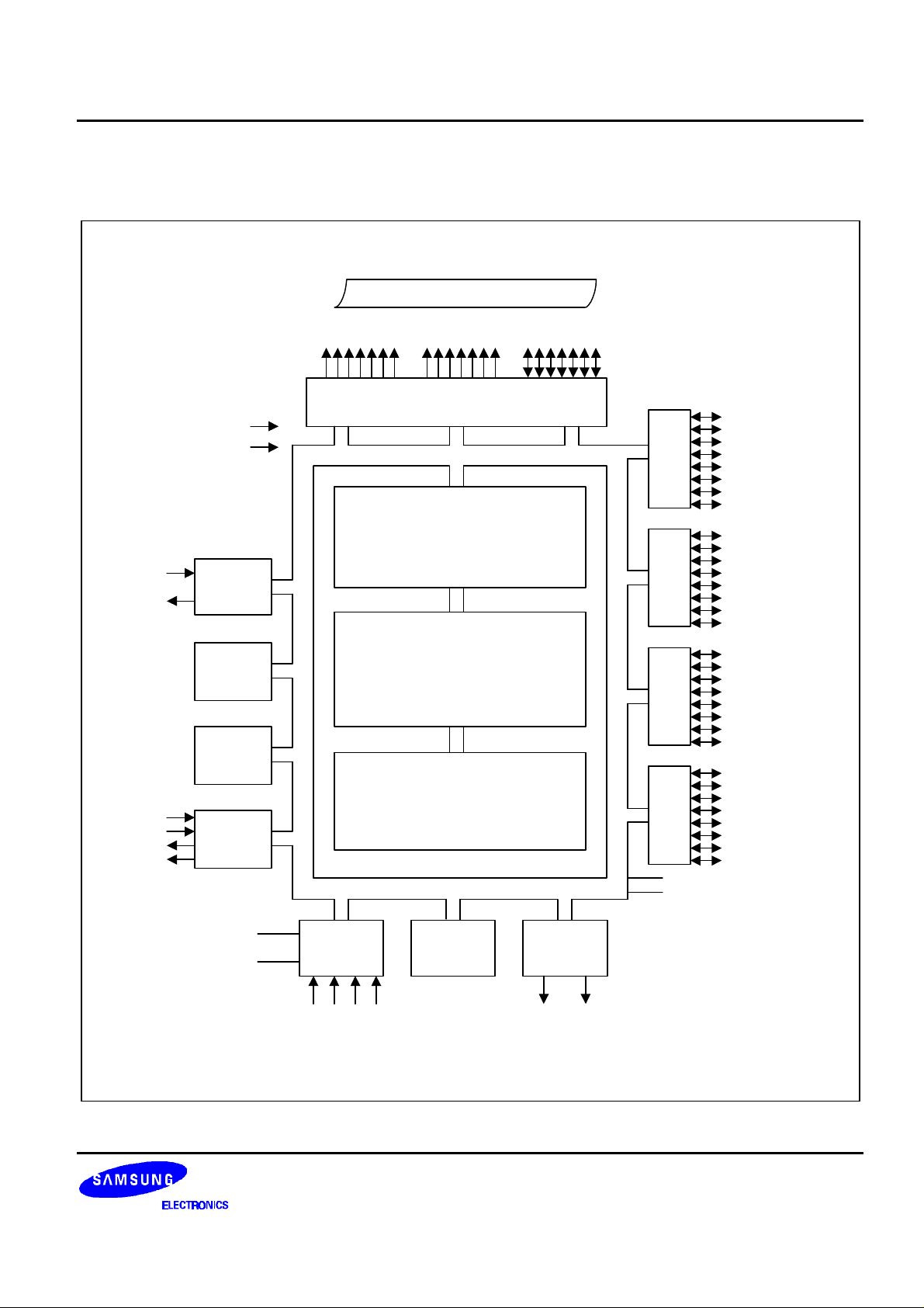
BLOCK DIAGRAM
External Address Data
XIN
XOUT
TCCK
TDCK
TCOUT
TDOUT
RESET
EA
Main
OSC
Timers
A and B
Basic
Timer
Timers
C and D
(A8-A15)
Port I/O
& Interrupt
Control
(A0-A7)
External Interface Block
SAM8 BUS
Watch-dog
Timer
SAM88 RC CPU
784-Byte Register File
SAM8 BUS
(D0-D7)
Port 0
Port 1
Port 2
Port 3
VDD1
VSS1
P0.0-P0.3/
ADC0-ADC3
P0.4-P0.7
P1.0-P1.7
TDCK,TCCK
TDCAP,TCCAP
TCOUT,TDOUT
PWM0,PWM1
P2.0-P2.3/
INT0-INT3
P2.4-P2.6
P2.7/WAIT
P3.0-P3.1/
A16-A17
P3.2, P3.3/
CS0-CS1
P3.4
AVSS (Internally)
AVREF
A/D
Converter
ADC0/P0.0ADC3/P0.3
4-Kbyte
ROM
PWM0 PWM1
Figure 1-1. S3C84A4 Block Diagram
PWM
Module
1-3
PRODUCT OVERVIEW S3C84A4/P84A4
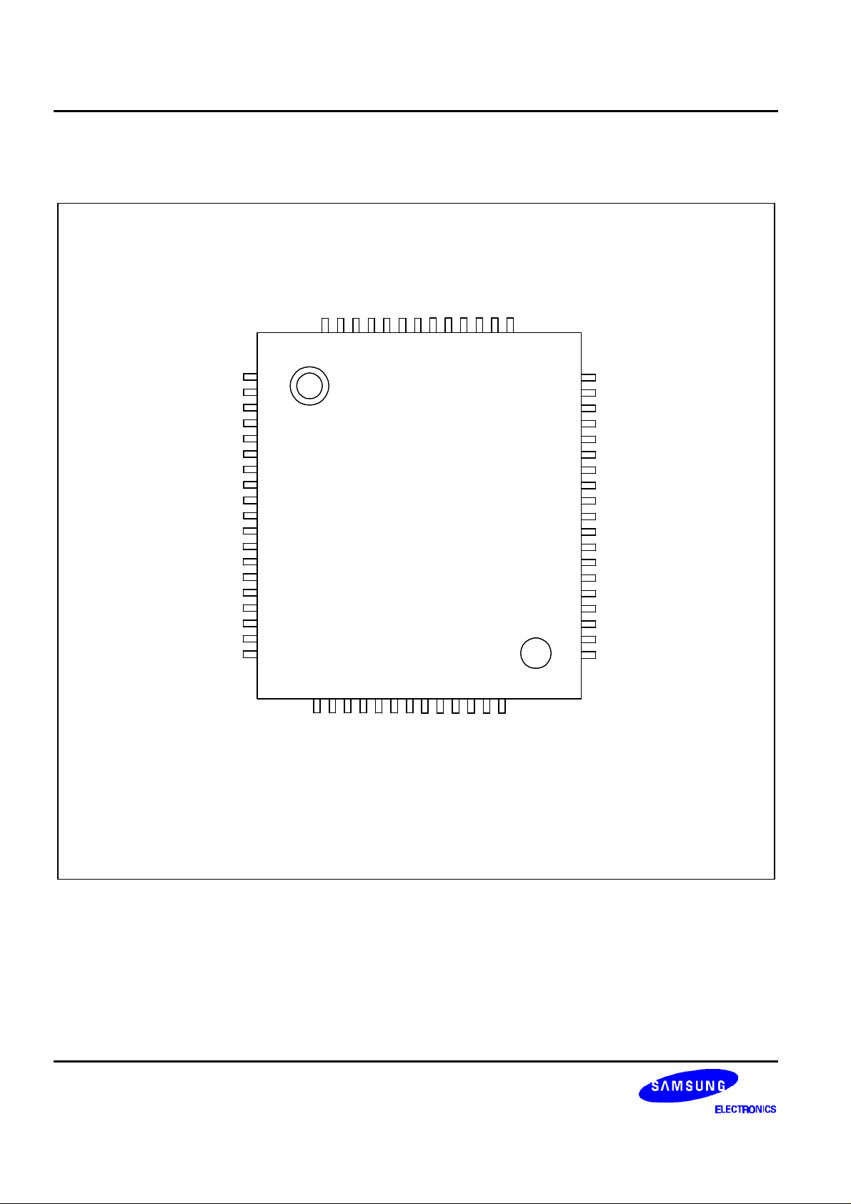
PIN ASSIGNMENT
A10
A11
A12
A13
A14
A15
64
63
62
61
60
59
A9
58
A8
57
A7
56
A6
55
A5
54
A4
53
A3
53
PM
DM
RD
WR
P3.4
CS1/P3.3
CS0/P3.2
A17/P3.1
VDD
VSS
XOUT
XIN
TEST/EA
A16/P3.0
WAIT/P2.7
RESET
P2.6
P2.5
P2.4
1
2
3
4
5
6
7
8
9
10
11
12
13
14
15
16
17
18
19
23
22
21
20
P2.0/INT0
P2.1/INT1
P2.2/INT2
P2.3/INT3
S3C84A4
(64-QFP)
28
27
26
25
24
P1.3/TCCAP
P1.4/TCOUT
P1.5/TDOUT
P1.6/PWM0
P1.7/PWM1
32
31
30
29
P0.7
P1.0/TDCK
P1.1/TCCK
P1.2/TDCAP
51
50
49
48
47
46
45
44
43
42
41
40
39
38
37
36
35
34
33
A2
A1
A0
D7
D6
D5
D4
D3
D2
D1
D0
AVREF
P0.0/ADC0
P0.1/ADC1
P0.2/ADC2
P0.3/ADC3
P0.4
P0.5
P0.6
1-4
Figure 1-2. S3C84A4 Pin Assignments

S3C84A4/P84A4 PRODUCT OVERVIEW
PIN DESCRIPTIONS
Table 1-1. S3C84A4/P84A4 Pin Descriptions
Pin
Name
P0.0–P0.7 I/O Bit programmable port; input or output mode
P1.0–P1.7 I/O Bit programmable port; input or output mode
P2.0–P2.7 I/O General I/O port with normal input or push-pull
P3.0–P3.4 I/O General I/O port with bit programmable pins.
Pin
Type
Pin
Description
selected by software; normal input or push-pull
Software assignable pull-up.
Alternately, P0.0–P0.3 can be use as a ADC input
port with 8-bit resolution.
selected by software ; normal input or push-pull.
Software assignable pull-up. Respectively, each pin
can serve as:
P1.0 / timer D clock input (TDCK)
P1.1 / timer C clock input (TCCK)
P1.2 / timer D capture input (TDCAP)
P1.3 / timer C capture input (TCCAP)
P1.4 / timer C out (TCOUT) / PWM out (TCPWM)
P1.5 / timer D out (TDOUT) / PWM out (TDPWM)
P1.6 / PWM0 output port
P1.7 / PWM1 output port
output. Software assignable pull-up.
Bit programmable;
Alternately, P2.0– P2.3 can be used as inputs for
external interrupts,INT0– INT3( with noise filter and
interrupt control). INT0/INT1 are level interrupts
Normal input or push-pull output with software
assignable pull-up. Input or output mode is
selectable by software. P3.0-P3.1 can alternately be
used as outputs of high address (A16,A17).
P3.2–P3.3 can alternately be used as outputs for
embedded chip selection output.
P3.0 / A16
P3.1 / A17
P3.2 / CS0
P3.3 / CS1
Circuit
Type
2,3 39–32 ADC0–
3,5 31–24 TDCK
3,4,5 23–17
3,5 14,
Pin
Number
15
8–5
Share
Pins
ADC3
TCCK
TDCAP
TCCAP
TCOUT/
TCPWM
TDOUT/
TDPWM
PWM0
PWM1
INT0–INT3
A16, A17
CS0,CS1
1-5
PRODUCT OVERVIEW S3C84A4/P84A4
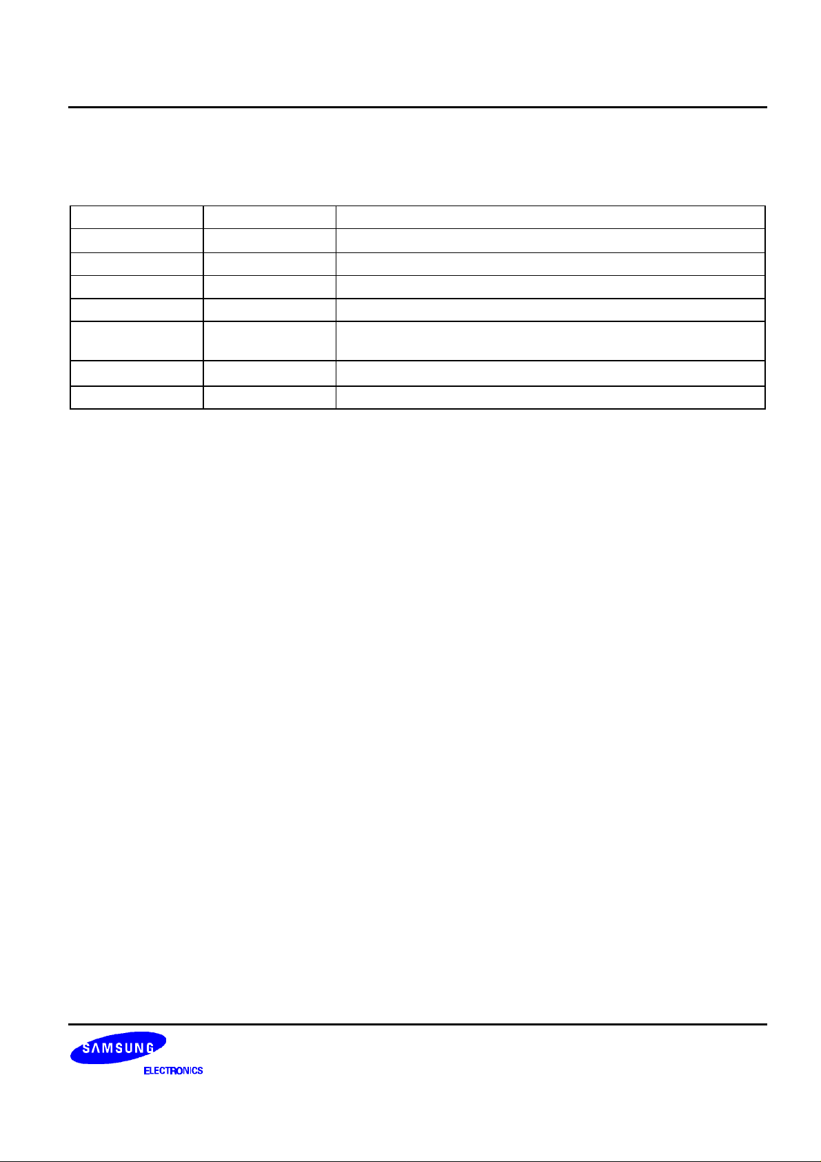
Table 1-1. S3C84A4/P84A4 Pin Descriptions (Continued)
Pin
Name
ADC0-ADC3 I Analog input pins for A/D converter module.
Pin
Type
Pin
Description
Circuit
Type
Pin
Number
Share
2 39–36 P0.0-P0.3
Pins
Alternatively, used as general-purpose I/O
AV
REF
– A/D converter reference voltage
– 40 –
AVSS is connected to ground internally
PWM0,
O Pulse width modulation output pins 5 25,24 P1.6, P1.7
PWM1
INT0-INT3 I External interrupt input pins 4 23-20 P2.0–P2.3
TCCK, TDCK I External clock input for timer C and timer D 3 30,31 P1.1/P1.0
TCCAP,
I Timer C/ Timer D capture input 3 28,29 P1.3/P1.2
TDCAP
TCOUT,
TDOUT
WAIT
O Timer C/D 8-bit PWM mode output or counter
match toggle output
I Input pin for the slow memory timing signal
5 27,26 P1.4, P1.5
5 15 P2.7
from the external interface
I
RESET
System reset pin (pull-up resistor: 50 kΩ)
EA I 5V: ROMless operating
1 16 –
– 13 –
0V: internal 4K and external 60K
addressing mode
VDD, V
XIN, X
SS
OUT
– Power input pins – 9,10 –
– Main oscillator pins – 12,11 –
A0–A15 O Address output for external device 6 49–64 –
D0–D7 I/O Data I/O for external device 7 41–48 –
PM, DM
RD,WR
A16, A17
CS0–CS1
O External memory selection output – 1,2 –
O External memory read/write output – 3, 4 –
O Extended memory high address output 5 14, 8 P3.0, P3.1
O Embedded chip selection output 5 7, 6 P3.2, P3.3
1-6
S3C84A4/P84A4 PRODUCT OVERVIEW
PIN CIRCUITS
Table 1-2. Pin Circuit Assignments for the S3C84A4/P84A4
Circuit Number Circuit Type S3C8414X Assignments
1 Input
2 I/O A/D converter input pins, ADC0–ADC3, P0.0–P0.3
3 I/O Port 0, 2, and 3
4 I/O P2 (INT0–INT3)
5 I/O P1 (TDCK, TCCK, TDCAP, TCCAP, TCOUT, TDOUT, TCPWM,
6 Output
7 I/O D0–D7
RESET pin
TDPWM, PWM0, PWM1)
A0–A15, PM, DM, RD, WR
1-7
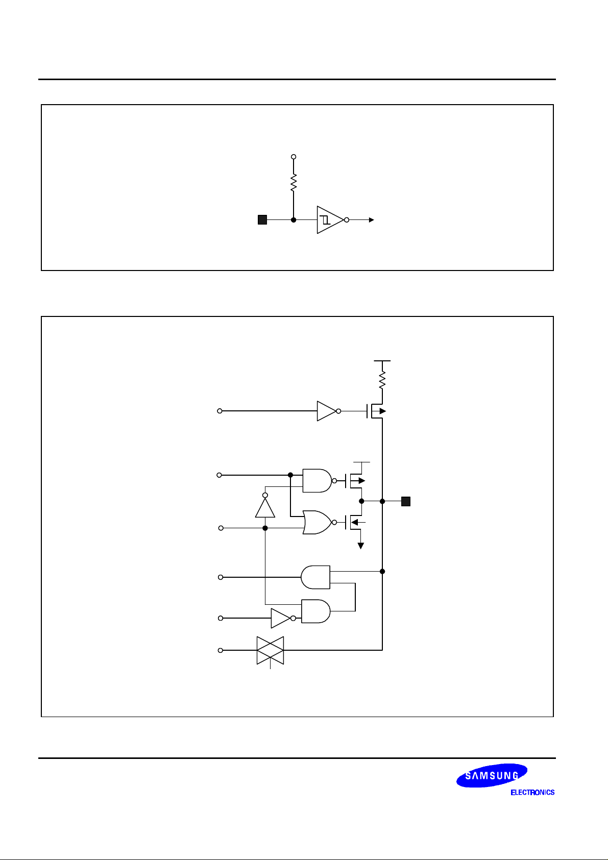
PRODUCT OVERVIEW S3C84A4/P84A4
VDD
Pull-up
Resistor
(Typical 50 kΩ)
Input
Figure 1-4. Pin Circuit Type 1 (RESETRESET)
VDD
Pull-Down
Enable
Data
Output
Disable
Normal
Input
ADC Port
Selection
ADC In
Pull-up
Resistor
VDD
I/O
Vss
1-8
Enable ADC
Figure 1-5. Pin Circuit Type 2 (ADC0–ADC3)
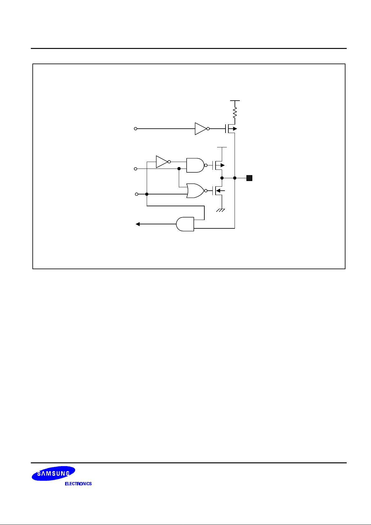
S3C84A4/P84A4 PRODUCT OVERVIEW
VDD
Pull-Up
Enable
VDD
Data
I/O
Output
Disable
Normal
Input
Figure 1-6. Pin Circuit Type 3
1-9
 Loading...