

Samsung S3C8095, S3P8095 Datasheet
S3C8095/P8095 PRODUCT OVERVIEW
1 PRODUCT OVERVIEW
S3C8-SERIES MICROCONTROLLERS
Samsung's S3C8 series of 8-bit single-chip CMOS microcontrollers offers a fast and efficient CPU, a wide range
of integrated peripherals, and various mask-programmable ROM sizes. Important CPU features include:
— Efficient register-oriented architecture
— Selectable CPU clock sources
— Idle and Stop power-down mode release by interrupt
— Built-in basic timer with watchdog function
A sophisticated interrupt structure recognizes up to eight interrupt levels. Each level can have one or more
interrupt sources and vectors. Fast interrupt processing (within a minimum six CPU clocks) can be assigned to
specific interrupt levels.
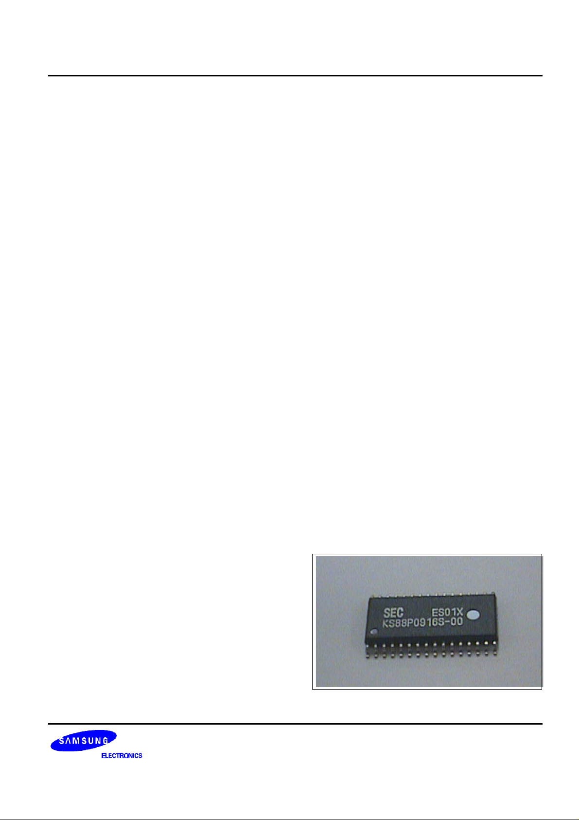
S3C8095/P8095 MICROCONTROLLER
The S3C8095/P8095 single-chip CMOS
microcontroller is fabricated using a highly advanced
CMOS process and is based on Samsung’s newest
CPU architecture.
The S3C8095 is the microcontroller which has 16Kbytes mask-programmable ROM.
The S3P8095 is the microcontroller which has 16Kbytes one-time-programmable EPROM.
Using a proven modular design approach, Samsung
engineers developed the S3C8095/P8095 by
integrating the following peripheral modules with the
powerful SAM87 core:
— Four programmable I/O ports, including three
8-bit ports and one 2-bit port, for a total of 26
pins.
— One 8-bit timer/counter and one 16-bit
timer/counter with selectable operating modes.
— One 8-bit counter with auto-reload function and
one-shot or repeat control.
The S3C8095 is a versatile general-purpose
microcontroller. It is currently available in a 32-pin
SOP and SDIP package.
— Twelve bit-programmable pins for external
interrupts.
— One 8-bit basic timer for oscillation stabilization
and watchdog functions (system reset).
Figure 1-1. S3C8095 Microcontroller
1-1

PRODUCT OVERVIEW S3C8095/P8095
FEATURES
CPU
• SAM87 CPU core
Memory
• 16K-byte internal program memory (ROM)
• 317-byte internal register file
Instruction Set
• 78 instructions
• IDLE and STOP instructions added for powerdown modes
Instruction Execution Time
• 750 ns at 8-MHz f
(minimum)
OSC
Interrupts
• Six interrupt levels and 18 interrupt sources
• 15 vectors (14 sources have a dedicated vector
address and four sources share a single vector)
• Fast interrupt processing feature (for one
selected interrupt level)
Timers and Timer/Counters
• One programmable 8-bit basic timer (BT) for
oscillation stabilization control or watchdog timer
(software reset) function
• One 8-bit timer/counter (Timer 0) with three
operating modes; Interval, Capture and PWM
• One 16-bit timer/counter (Timer 1) with two
operating modes; Interval and Capture
Carrier Frequency Generator
• One 8-bit counter with auto-reload function and
one-shot or repeat control (Counter A)
Operating Temperature Range
• – 20°C to + 85°C
Operating Voltage Range
• 2.0 V to 5.5 V at 4 MHz f
• 2.4 V to 5.5 V at 8 MHz f
OSC
OSC
Package Type
I/O Ports
• Three 8-bit I/O ports (P0–P2) and one 2-bit port
(P3) for a total of 26 bit-programmable pins
• Twelve input pins for external interrupts
• 32-pin SOP
• 32-pin SDIP
1-2
S3C8095/P8095 PRODUCT OVERVIEW
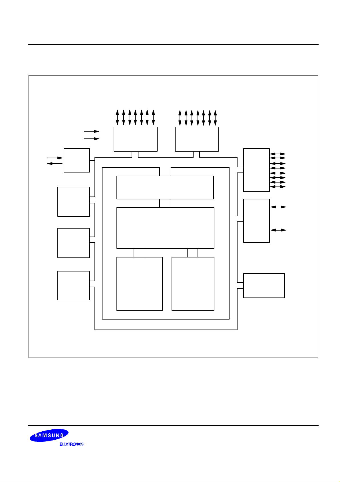
BLOCK DIAGRAM
P0.0–P0.7
P1.0–P1.7
PORT 1
RESET
TEST
(INT0–INT4)
PORT 0
X
X
IN
OUT
MAIN
OSC
8-BIT
BASIC
TIMER
8-BIT
TIMER/
COUNTER
16-BIT
TIMER/
COUNTER
INTERNAL BUS
I/O PORT and INTERRUPT
CONTROL
SAM8 CPU
16-KB ROM
317-BYTES
REGISTER
FILE
PORT2
P3.0/T0PWM/
PORT 3
CARRIER
GENERATOR
(COUNTER A)
T0CAP/T1CAP
P3.1/REM/T0CK
P2.0–P2.3
(INT5–INT8)
P2.4–P2.7
Figure 1-2. Block Diagram
1-3
PRODUCT OVERVIEW S3C8095/P8095
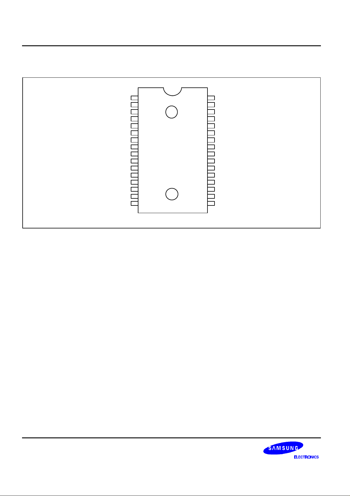
PIN ASSIGNMENTS
V
X
X
OUT
TEST
P2.0 / INT5
P2.1 / INT6
P2.2 / INT7
P2.3 / INT8
P0.0 / INT0
P0.1 / INT1
P0.2 / INT2
P0.3 / INT3
P0.4 / INT4
P0.5 / INT4
P0.6 / INT4
P0.7 / INT4
SS
1
IN
2
3
4
5
6
7
S3C8095
8
32-SOP/SDIP
9
(Top View)
10
11
12
13
14
15
16
32
31
30
29
28
27
26
25
24
23
22
21
20
19
18
17
V
DD
RESET
P3.1 / REM / T0CK
P3.0 / T0PWM / T0CAP / T1CAP
P2.7
P2.6
P2.5
P2.4
P1.7
P1.6
P1.5
P1.4
P1.3
P1.2
P1.1
P1.0
Figure 1-3. Pin Assignment Diagram (32-Pin SOP/SDIP Package)
1-4
S3C8095/P8095 PRODUCT OVERVIEW
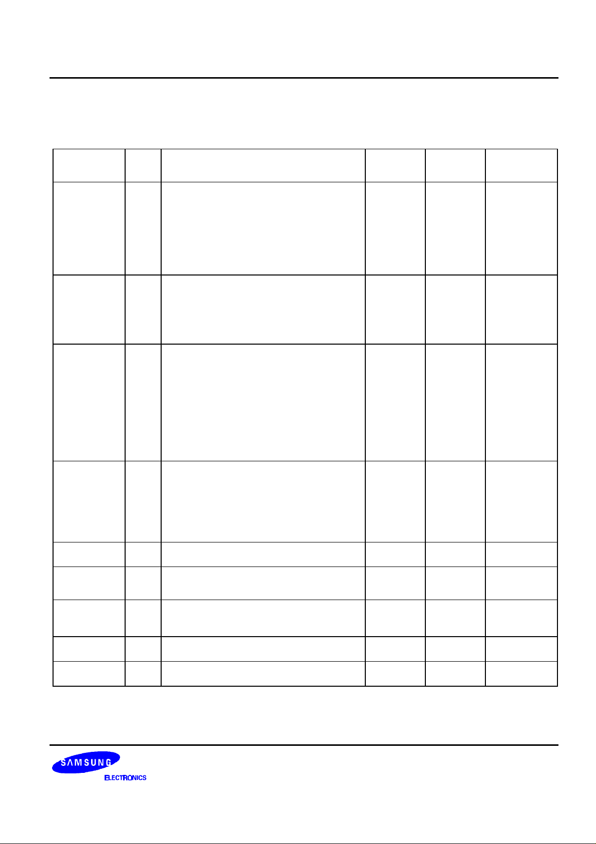
PIN DESCRIPTIONS
Table 1-1. Pin Descriptions
Pin
Names
Pin
Type
Pin
Description
P0.0–P0.7 I/O I/O port with bit-programmable pins.
Configurable to input or push-pull output
mode. Pull-up resistors are assignable by
software. Pins can be assigned individually
as external interrupt inputs with noise filters,
interrupt enable/ disable, and interrupt
pending control.
P1.0–P1.7 I/O I/O port with bit-programmable pins.
Configurable to Schmitt trigger input mode
or output mode. Pin circuits are either pushpull or n-channel open-drain type. Pull-up
resistors are assignable by software.
P2.0–P2.3
P2.4–P2.7
I/O General-purpose I/O port with bit-
programmable pins. Configurable to
Schmitt trigger input mode, push-pull output
mode, or n-channel open-drain output
mode. Pull-up resistors are assignable by
software. Lower nibble pins, P2.3–P2.0, can
be assigned as external interrupt inputs with
noise filters, interrupt enable/disable, and
interrupt pending control.
Circuit
Type
Pin No. Shared
Functions
1 9–16 INT0–INT4
3 17–24 –
2
3
5–8,
25–28
INT5–INT8
–
P3.0
P3.1
I/O 2-bit I/O port with bit-programmable pins.
Configurable to Schmitt trigger input mode,
push-pull output mode, or n-channel opendrain output mode. Pull-up resistors are
assignable by software. The two port 3 pins
have high current drive capability.
XIN, X
RESET
OUT
– System clock input and output pins – 2, 3 –
I System reset signal input pin with schmitt
trigger circuit.
TEST I Test signal input pin (for factory use only;
must be connected to VSS).
V
DD
V
SS
– Power supply input pin – 32 –
– Ground pin – 1 –
4 29
30
T0PWM/
T0CAP/
T1CAP/
REM/T0CK
5 31 –
– 4 –
1-5
PRODUCT OVERVIEW S3C8095/P8095
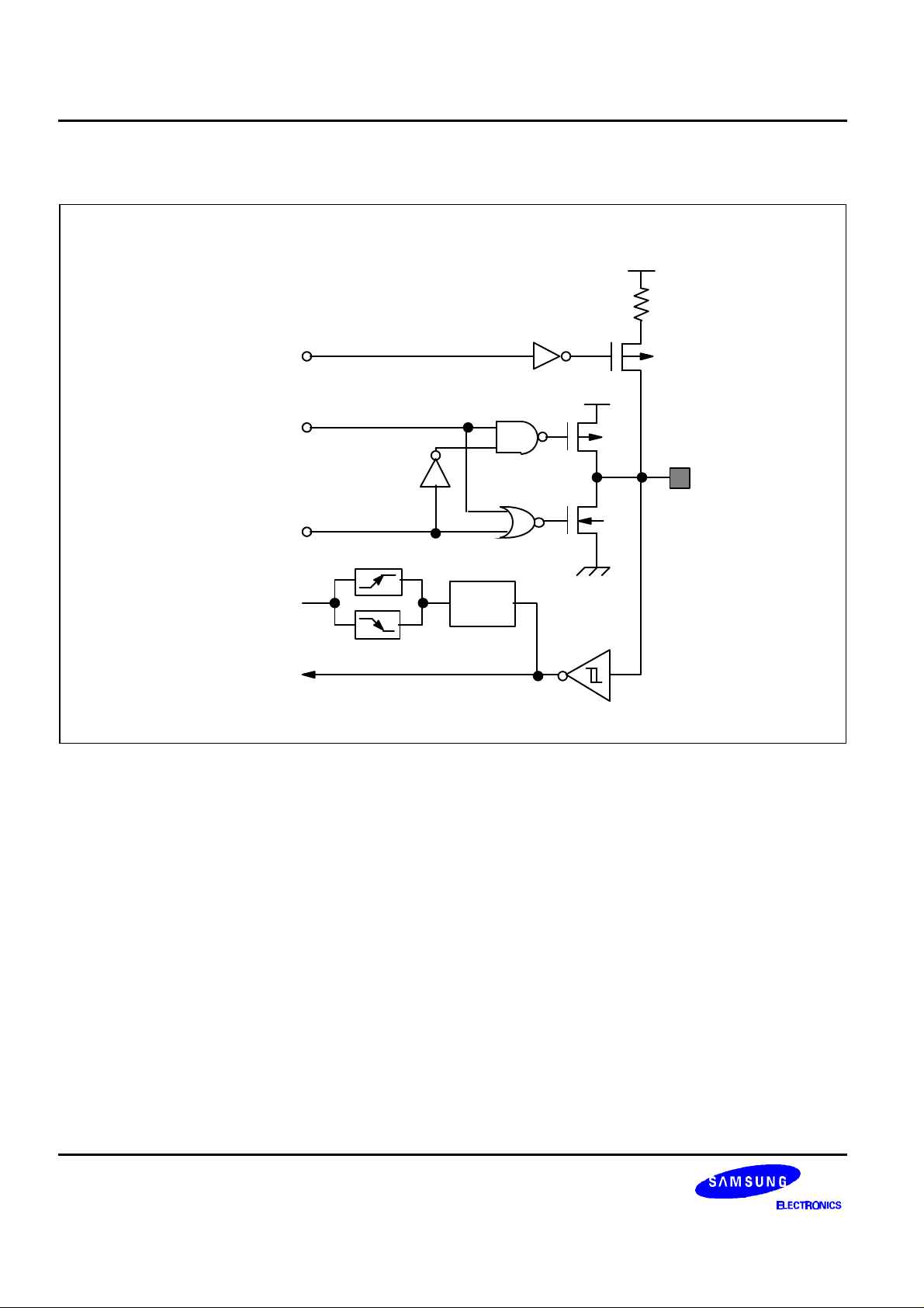
PIN CIRCUITS
V
DD
PULL-UP
RESISTOR
(Typical
PULL-UP
ENABLE
DATA
OUTPUT
DISABLE
V
DD
50 ΚΩ)
INPUT /
OUTPUT
INTERRUPT INPUT
IRQ6,7 (INT0-4)
NORMAL
INPUT
NOISE
FILTER
Figure 1-4. Pin Circuit Type 1 (Port 0)
V
SS
1-6
S3C8095/P8095 PRODUCT OVERVIEW
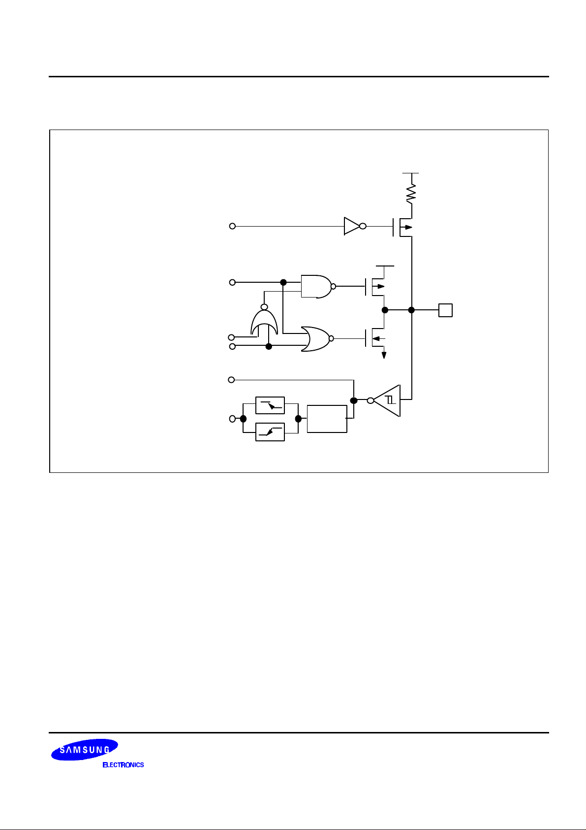
PIN CIRCUITS (Cont.)
V
DD
PULL-UP
RESISTOR
PULL-UP
ENABLE
DATA
OPEN-DRAIN
OUTPUT DISABLE
(Typical 50
V
DD
ΚΩ)
IN / OU T
NORMAL INPUT
EXTERNAL
INTERRUPT
IRQ5 (INT5-8)
Figure 1-5. Pin Circuit Type 2 (Ports 2.0–2.3)
V
SS
NOISE
FILTER
1-7
PRODUCT OVERVIEW S3C8095/P8095
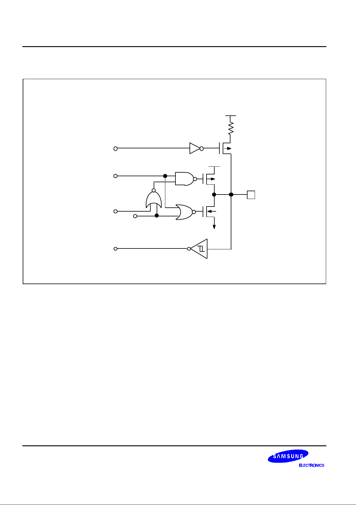
PIN CIRCUITS (Cont.)
V
DD
PULL-UP
RESISTOR
PULL-UP
ENABLE
DATA
(Typical 50
V
DD
ΚΩ)
OPENDRAIN
NORMAL INPUT
Figure 1-6. Pin Circuit Type 3 (Ports 1 and P2.4–P2.7)
OUTPUT
DISABLE
IN / OUT
V
SS
1-8
S3C8095/P8095 PRODUCT OVERVIEW
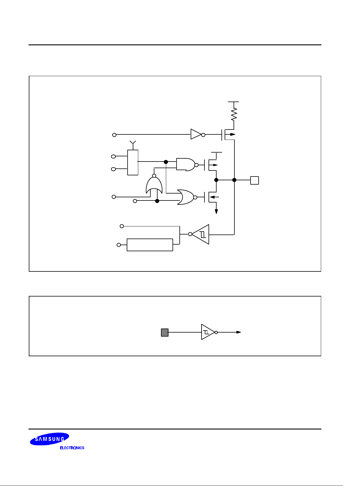
PIN CIRCUITS (Cont.)
V
DD
PULL-UP
RESISTOR
Typical
PULL-UP
ENABLE
PORT 3
DATA
ALTERNATIVE
OUTPUT
SELECT
M
U
X
DATA
(
V
DD
50 ΚΩ)
OPENDRAIN
NORMAL INPUT
ALTERNATIVE
INPUT
OUTPUT
DISABLE
NOISE F ILTER
Figure 1-7. Pin Circuit Type 4 (Port 3)
RESET
V
SS
IN / OUT
Figure 1-8. Pin Circuit Type 5 (RRESETESET)
1-9
 Loading...