

Page 1

Rev. 1.3, Feb. 2018
M393A2K43CB1
M393A2K43CB2
M393A2K40CB1
M393A2K40CB2
M393A4K40CB1
M393A4K40CB2
288pin Registered DIMM
based on 8Gb C-die
78FBGA with Lead-Free & Halogen-Free
(RoHS compliant)
datasheet
SAMSUNG ELECTRONICS RESERVES THE RIGHT TO CHANGE PRODUCTS, INFORMATION AND
SPECIFICATIONS WITHOUT NOTICE.
Products and specifications discussed herein are for reference purposes only. All information discussed
herein is provided on an "AS IS" basis, without warranties of any kind.
This document and all information discussed herein remain the sole and exclusive property of Samsung
Electronics. No license of any patent, copyright, mask work, trademark or any other intellectual property
right is granted by one party to the other party under this document, by implication, estoppel or otherwise.
Samsung products are not intended for use in life support, critical care, medical, safety equipment, or
similar applications where product failure could result in loss of life or personal or physical harm, or any
military or defense application, or any governmental procurement to which special terms or provisions
may apply.
For updates or additional information about Samsung products, contact your nearest Samsung office.
All brand names, trademarks and registered trademarks belong to their respective owners.
© 2018 Samsung Electronics Co., Ltd. All rights reserved.
- 1 -
Page 2

Rev. 1.3
Registered DIMM
datasheet
DDR4 SDRAM
Revision History
Revision No. History Draft Date Remark Editor
1.0 - First SPEC release 23th Feb. 2017 - J.Y.Lee
1.01 - Correction of Typo 7th Mar. 2017 - J.Y.Lee
1.02 - Correction of Typo 16th Mar. 2017 - J.Y.Lee
1.1 - Addition of DDR4-2666 5th Apr. 2017 - J.Y.Lee
1.2
1.3 - Add 2933Mbps. 6th Feb, 2018 Final J.H.Han
- Add Module codes.
: M393A2K43CB2, M393A2K40CB2 and M393A4K40CB2.
- Add IDD Spec tables for M393A2K43CB2, M393A2K40CB2 and
M393A4K40CB2.
- Update Physical Dimension.
1. Add dimensions for M393A2K43CB2, M393A2K40CB2 and
M393A4K40CB2.
2. Add PCB Hole for M393A4K40CB1.
- Correct typo. J.Y.Bae
13th Jun, 2017 Final J.Y.Bae
- 2 -
Page 3

Rev. 1.3
datasheet
DDR4 SDRAMRegistered DIMM
Table Of Contents
288pin Registered DIMM based on 8Gb C-die
1. DDR4 REGISTERED DIMM ORDERING INFORMATION ..................................................................................................................5
2. KEY FEATURES ..................................................................................................................................................................................5
3. ADDRESS CONFIGURATION .............................................................................................................................................................5
4. REGISTERED DIMM PIN CONFIGURATIONS (FRONT SIDE/BACK SIDE)......................................................................................6
5. PIN DESCRIPOTION ..........................................................................................................................................................................7
6. ON DIMM THERMAL SENSOR ...........................................................................................................................................................8
7. INPUT/OUTPUT FUNCTIONAL DESCRIPTION .................................................................................................................................9
8. REGISTERING CLOCK DRIVER SPECIFICATION ............................................................................................................................11
8.1 Timing & Capacitance Values.........................................................................................................................................................11
8.2 Clock Driver Characteristics ...........................................................................................................................................................11
9. FUNCTION BLOCK DIAGRAM: ...........................................................................................................................................................12
9.1 16GB, 2Gx72 Module (Populated as 2 rank of x8 DDR4 SDRAMs) .............................................................................................. 12
9.2 16GB, 2Gx72 Module (Populated as 1 rank of x4 DDR4 SDRAMs) .............................................................................................. 14
9.3 32GB, 4Gx72 Module (Populated as 2 ranks of x4 DDR4 SDRAMs).............................................................................................15
10. ABSOLUTE MAXIMUM RATINGS .....................................................................................................................................................17
10.1 Absolute Maximum DC Ratings.................................................................................................................................................... 17
11. AC & DC OPERATING CONDITIONS ...............................................................................................................................................17
12. AC & DC INPUT MEASUREMENT LEVELS......................................................................................................................................18
12.1 AC & DC Logic Input Levels for Single-Ended Signals................................................................................................................. 18
12.2 AC and DC Input Measurement Levels: VREF Tolerances. ......................................................................................................... 18
12.3 AC and DC Logic Input Levels for Differential Signals .................................................................................................................19
12.3.1. Differential Signals Definition ................................................................................................................................................19
12.3.2. Differential Swing Requirements for Clock (CK_t - CK_c) ....................................................................................................20
12.3.3. Single-ended Requirements for Differential Signals .............................................................................................................21
12.3.4. Address, Command and Control Overshoot and Undershoot specifications........................................................................ 22
12.3.5. Clock Overshoot and Undershoot Specifications.................................................................................................................. 23
12.3.6. Data, Strobe and Mask Overshoot and Undershoot Specifications ...................................................................................... 24
12.4 Slew Rate Definitions.................................................................................................................................................................... 25
12.4.1. Slew Rate Definitions for Differential Input Signals (CK) ......................................................................................................25
12.4.2. Slew Rate Definition for Single-ended Input Signals (CMD/ADD) ........................................................................................26
12.5 Differential Input Cross Point Voltage........................................................................................................................................... 27
12.6 CMOS rail to rail Input Levels .......................................................................................................................................................28
12.6.1. CMOS rail to rail Input Levels for RESET_n .........................................................................................................................28
12.7 AC and DC Logic Input Levels for DQS Signals........................................................................................................................... 29
12.7.1. Differential signal definition ...................................................................................................................................................29
12.7.2. Differential swing requirements for DQS (DQS_t - DQS_c).................................................................................................. 29
12.7.3. Peak voltage calculation method ..........................................................................................................................................30
12.7.4. Differential Input Cross Point Voltage ...................................................................................................................................31
12.7.5. Differential Input Slew Rate Definition ..................................................................................................................................32
13. AC and DC output Measurement levels .............................................................................................................................................33
13.1 Output Driver DC Electrical Characteristics..................................................................................................................................33
13.1.1. Alert_n output Drive Characteristic .......................................................................................................................................35
13.1.2. Output Driver Characteristic of Connectivity Test (CT) Mode............................................................................................... 36
13.2 Single-ended AC & DC Output Levels........................................................................................
13.3 Differential AC & DC Output Levels.............................................................................................................................................. 37
13.4 Single-ended Output Slew Rate ...................................................................................................................................................38
13.5 Differential Output Slew Rate .......................................................................................................................................................39
13.6 Single-ended AC & DC Output Levels of Connectivity Test Mode ...............................................................................................40
13.7 Test Load for Connectivity Test Mode Timing ..............................................................................................................................41
14. IDD SPEC TABLE ..............................................................................................................................................................................42
15. INPUT/OUTPUT CAPACITANCE ......................................................................................................................................................49
16. SPEED BIN ........................................................................................................................................................................................50
16.1 Speed Bin Table Note................................................................................................................................................................... 56
17. IDD and IDDQ Specification Parameters and Test conditions ...........................................................................................................57
17.1 IDD, IPP and IDDQ Measurement Conditions.............................................................................................................................. 57
18. DIMM IDD SPECIFICATION DEFINITION .........................................................................................................................................60
19. TIMING PARAMETERS BY SPEED GRADE ....................................................................................................................................72
19.1 Rounding Algorithms ...................................................................................................................................................................78
19.2 The DQ input receiver compliance mask for voltage and timing .................................................................................................. 79
..................................................37
- 3 -
Page 4

Rev. 1.3
datasheet
19.3 Command, Control, and Address Setup, Hold, and Derating .......................................................................................................82
19.4 DDR4 Function Matrix ..................................................................................................................................................................84
20. PHYSICAL DIMENSIONS ..................................................................................................................................................................86
20.1 1Gx8 based 2Gx72 Module (2 Ranks) - M393A2K43CB1 and M393A2K43CB2.........................................................................86
20.1.1. 2Gx72 DIMM, populated as two physical rank of x8 DDR4 SDRAMs ..................................................................................86
20.2 2Gx4 based 2Gx72 Module (1 Rank) - M393A2K40CB1 and M393A2K40CB2 .......................................................................... 87
20.2.1. 2Gx72 DIMM, populated as one physical rank of x4 DDR4 SDRAMs .................................................................................. 87
20.3 2Gx4 based 4Gx72 Module (2 Ranks) - M393A4K40CB1 ........................................................................................................... 88
20.3.1. 4Gx72 DIMM, populated as two physical ranks of x4 DDR4 SDRAMs ................................................................................88
20.4 2Gx4 based 4Gx72 Module (2 Ranks) - M393A4K40CB2 ........................................................................................................... 89
20.4.1. 4Gx72 DIMM, populated as two physical ranks of x4 DDR4 SDRAMs ................................................................................89
DDR4 SDRAMRegistered DIMM
- 4 -
Page 5
Rev. 1.3
datasheet
DDR4 SDRAMRegistered DIMM
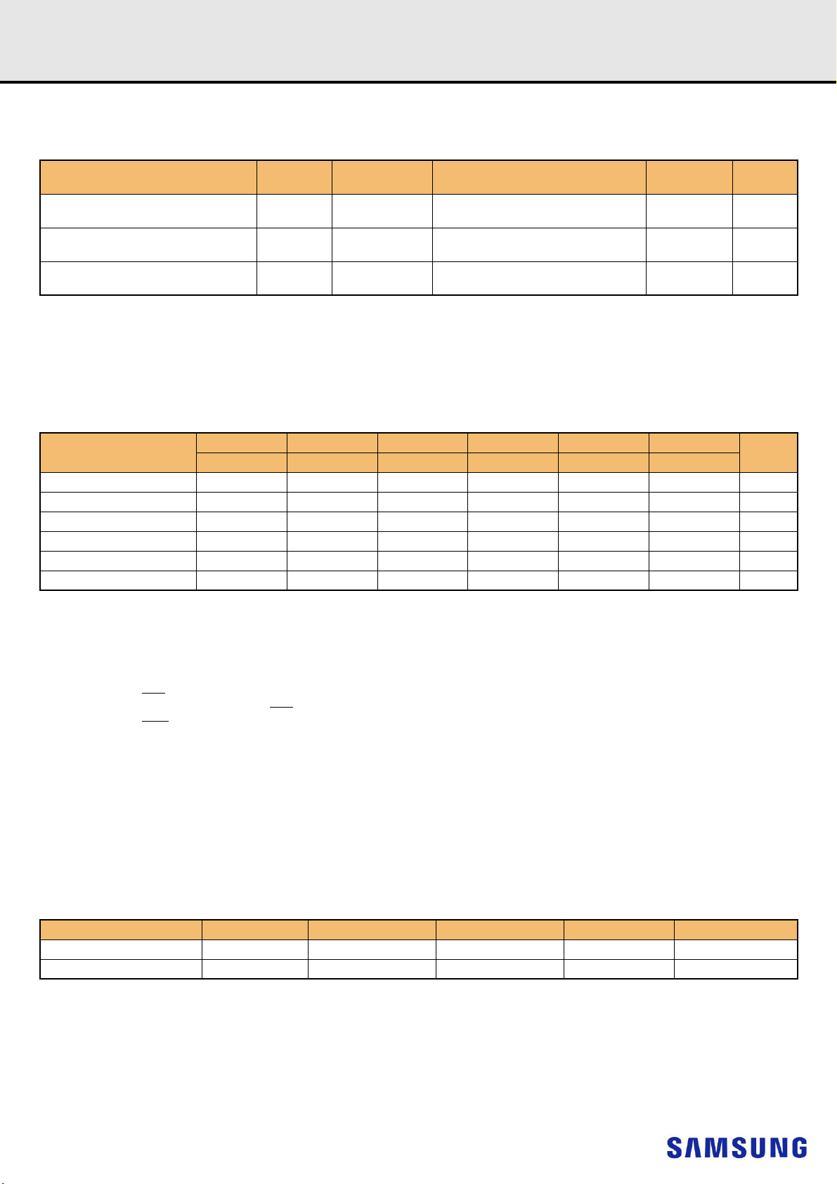
1. DDR4 REGISTERED DIMM ORDERING INFORMATION
[Table 1] Ordering Information Table
Part Number
M393A2K43CB1-CRC
M393A2K43CB2-CTD/VF
M393A2K40CB1-CRC
M393A2K40CB2-CTD/VF
M393A4K40CB1-CRC
M393A4K40CB2-CTD/VF
NOTE :
1) "##"- RC/TD/VF.
2) RC(2400Mbps 17-17-17)/TD(2666Mbps 19-19-19)/VF(2933Mbps 21-21-21).
- Backward compatible to lower frequency.
2)
Density Organization
16GB 2Gx72 1Gx8(K4A8G085WC-BC##)*18 2 31.25mm
16GB 2Gx72 2Gx4(K4A8G045WC-BC##)*18 1 31.25mm
32GB 4Gx72 2Gx4(K4A8G045WC-BC##)*36 2 31.25mm
Component Composition
1)
Number of
Rank
2. KEY FEATURES
[Table 2] Speed Bins
Speed
tCK(min) 1.25 1.071 0.937 0.833 0.75 0.682 ns
CAS Latency 11 13 15 17 19 21 nCK
tRCD(min) 13.75 13.92 14.06 14.16 14.25 14.32 ns
tRP(min) 13.75 13.92 14.06 14.16 14.25 14.32 ns
tRAS(min) 35 34 33 32 32 32 ns
tRC(min) 48.75 47.92 47.06 46.16 46.25 46.32 ns
DDR4-1600 DDR4-1866 DDR4-2133 DDR4-2400 DDR4-2666 DDR4-2933
11-11- 11 13-13-13 15-15-15 17-17-17 19-19-19 21-21-21
Height
Unit
• JEDEC standard 1.2V ± 0.06V Power Supply
•V
• 800 MHz fCK for 1600Mb/sec/pin,933 MHz fCK for 1866Mb/sec/pin, 1067MHz fCK for 2133Mb/sec/pin,1200MHz fCK for 2400Mb/sec/pin, 1333MHz
• 16 Banks (4 Bank Groups)
• Programmable CAS Latency: 10,11,12,13,14,15,16,17,18,19,20,21
• Programmable Additive Latency (Posted CAS): 0, CL - 2, or CL - 1 clock
• Programmable CAS Write Latency (CWL) = 9,11 (DDR4-1600), 10,12 (DDR4-1866), 11,14 (DDR4-2133), 12,16 (DDR4-2400), 14,18 (DDR4-2666)
• Burst Length: 8 , 4 with tCCD = 4 which does not allow seamless read or write [either On the fly using A12 or MRS]
• Bi-directional Differential Data Strobe
• On Die Termination using ODT pin
• Average Refresh Period 7.8us at lower then T
• Asynchronous Reset
= 1.2V ± 0.06V
DDQ
for 2666Mb/sec/pin and 1467MHz fCK for 2933Mb/sec/pin.
f
CK
and 16, 20 (DDR4-2933)
85C, 3.9us at 85C < T
CASE
CASE
95C
3. ADDRESS CONFIGURATION
Organization Row Address Column Address Bank Group Address Bank Address Auto Precharge
1Gx8(8Gb) based Module A0-A15 A0-A9 BG0-BG1 BA0-BA1 A10/AP
2Gx4(8Gb) based Module A0-A16 A0-A9 BG0-BG1 BA0-BA1 A10/AP
- 5 -
Page 6
Rev. 1.3
datasheet
4. REGISTERED DIMM PIN CONFIGURATIONS
DDR4 SDRAMRegistered DIMM
(FRONT SIDE/BACK SIDE)
Pin Front Pin Back Pin Front Pin Back Pin Front Pin Back Pin Front Pin Back
12V
3
,NC
145
12V3,NC
1
2 VSS 146 VREFCA 41
3 DQ4 147 VSS 42 VSS 186 DQS3
4 VSS 148 DQ5 43 DQ30 187 VSS 81 BA0 225 A10/AP 120 VSS 264 DQ49
5 DQ0 149 VSS 44 VSS 188 DQ31 82 RAS
6 VSS 150 DQ1 45 DQ26 189 VSS 83 VDD 227 RFU 122
TDQS9_t,
7
DQS9_t
TDQS9_c,
8
DQS9_c
9 VSS 153 DQS0
151 VSS 46 VSS 190 DQ27 84 S0
152 DQS0
_c
_t
10 DQ6 154 VSS 49 CB0 193 VSS 87 ODT0 231 VDD 126 DQ50 270 VSS
11 VSS 155 DQ7 50 VSS 194 CB1 88 VDD 232 A13 127 VSS 271 DQ51
12 DQ2 156 VSS 51
13 VSS 157 DQ3 52
14 DQ12 158 VSS 53 VSS 197 DQS8
15 VSS 159 DQ13 54 CB6 198 VSS 92 VDD 236 VDD 131 VSS 275 DQ57
16 DQ8 160 VSS 55 VSS 199 CB7 93 C0,CS2
17 VSS 161 DQ9 56 CB2 200 VSS 94 VSS 238 SA2 133
TDQS10_t,
18
DQS10_t
TDQS10_c,
19
DQS10_c
20 VSS 164 DQS1
162 VSS 57 VSS 201 CB3 95 DQ36 239 VSS 134 VSS 278 DQS7
163 DQS1
_c
_t
21 DQ14 165 VSS 60 CKE0 204 VDD 98 VSS 242 DQ33 137 DQ58 281 VSS
22 VSS 166 DQ15 61 VDD 205 RFU 99
23 DQ10 167 VSS 62 ACT
24 VSS 168 DQ11 63 BG0 207 BG1 101 VSS 245 DQS4
25 DQ20 169 VSS 64 VDD 208 ALERT
26 VSS 170 DQ21 65 A12/BC
27 DQ16 171 VSS 66 A9 210 A11 104 DQ34 248 VSS 143 VPP 287 VPP
28 VSS 172 DQ17 67 VDD 211 A7 105 VSS 249 DQ35 144 RFU 288
TDQS11_t,
29
DQS11_t
TDQS11_c,
30
DQS11_c
31 VSS 175 DQS2
173 VSS 68 A8 212 VDD 106 DQ44 250 VSS
174 DQS2
_c
_t
32 DQ22 176 VSS 71 A3 215 VDD 109 VSS 253 DQ41
33 VSS 177 DQ23 72 A1 216 A2 110
34 DQ18 178 VSS 73 VDD 217 VDD 111
35 VSS 179 DQ19 74 CK0
36 DQ28 180 VSS 75 CK0
37 VSS 181 DQ29 76 VDD 220 VDD 114 VSS 258 DQ47
38 DQ24 182 VSS 77 VTT 221 VTT 115 DQ42 259 VSS
39 VSS 183 DQ25 KEY 116 VSS 260 DQ43
TDQS12_t,
40
DQS12_t
TDQS12_c,
DQS12_c
184 VSS 78 EVENT
185 DQS3
_c
79 A0 223 VDD 118 VSS 262 DQ53
_t
80 VDD 224 BA1 119 DQ48 263 VSS
_n
_n
222 PARITY 117 DQ52 261 VSS
/A16 226 VDD 121
_n
228 WE_n/A14 123 VSS 267 DQS6
TDQS15_t,
DQS15_t
TDQS15_c,
DQS15_c
265 VSS
266 DQS6
47 CB4 191 VSS 85 VDD 229 VDD 124 DQ54 268 VSS
48 VSS 192 CB5 86 CAS_n/A15 230 NC 125 VSS 269 DQ55
TDQS17_t,
DQS17_t
TDQS17_c,
DQS17_c
58 RESET
195 VSS 89 S1
196 DQS8
_n
202 VSS 96 VSS 240 DQ37 135 DQ62 279 VSS
_c
90 VDD 234 A17 129 VSS 273 DQ61
_t
91 ODT1 235 NC,C2 130 DQ56 274 VSS
_n
233 VDD 128 DQ60 272 VSS
_n
,NC 237 NC,CS3_c,C1 132
TDQS16_t,
DQS16_t
TDQS16_c,
DQS16_c
276 VSS
277 DQS7
59 VDD 203 CKE1 97 DQ32 241 VSS 136 VSS 280 DQ63
TDQS13_t,
DQS13_t
_n
206 VDD 100
_n
_n
209 VDD 103 VSS 247 DQ39 142 VPP 286 VPP
TDQS13_c,
DQS13_c
102 DQ38 246 VSS 141 SCL 285 SDA
243 VSS 138 VSS 282 DQ59
244 DQS4
_c
139 SA0 283 VSS
_t
140 SA1 284 VDDSPD
VPP
69 A6 213 A5 107 VSS 251 DQ45
70 VDD 214 A4 108 DQ40 252 VSS
_t
_c
218 CK1
219 CK1
TDQS14_t,
DQS14_t
TDQS14_c,
DQS14_c
_t
112 VS S 25 6 D QS5
_c
113 DQ 46 25 7 V SS
254 VSS
255 DQS5
_c
_t
_c
_t
_c
_t
4
NOTE :
1) VPP is 2.5V DC.
2) Pin 230 is defined as NC for UDIMMs, RDIMMs and LRDIMMs. Pin 230 is defined as SAVE_n for NVDIMMs.
3) Pins 1 and 145 are defined as NC for UDIMMs, RDIMMs and LRDIMMs. Pins 1 and 145 are defined as 12V for Hybrid /NVDIMM
4) The 5th VPP is required on all modules. DIMMs.
- 6 -
Page 7
Rev. 1.3
datasheet
DDR4 SDRAMRegistered DIMM
5. PIN DESCRIPOTION
Pin Name Description Pin Name Description
1)
A0–A17
BA0, BA1 Register bank select input SDA I
BG0, BG1 Register bank group select input SA0–SA2 I
RAS_n
CAS_n
WE_n
CS0_n, CS1_n,
CS2_n, CS3_n
CKE0, CKE1 Register clock enable lines input VSS Power supply return (ground)
ODT0, ODT1 Register on-die termination control lines input VDDSPD Serial SPD/TS positive power supply
ACT_n Register input for activate input ALERT_n Register ALERT_n output
DQ0–DQ63 DIMM memory data bus RESET_n Set Register and SDRAMs to a Known State
CB0–CB7 DIMM ECC check bits EVENT_n SPD signals a thermal event has occurred
DQS0_t–
DQS17_t
DQS0_c–
DQS17_c
CK0_t, CK1_t
CK0_c, CK1_c
Register address input SCL I2C serial bus clock for SPD/TS and register
2
C serial bus data line for SPD/TS and register
2
C slave address select for SPD/TS and register
2)
Register row address strobe input PAR Register parity input
3)
Register column address strobe input VDD SDRAM core power supply
4)
Register write enable input VPP SDRAM activating power supply
DIMM Rank Select Lines input VREFCA SDRAM command/address reference supply
Data Buffer data strobes
(positive line of differential pair)
Data Buffer data strobes
(negative line of differential pair)
Register clock input (positive line of differential pair)
Register clocks input (negative line of differential
pair)
VTT
RFU Reserved for future use
SDRAM I/O termination supply
NOTE :
1) Address A17 is only valid for 16Gb x4 based SDRAMs.
2) RAS_n is a multiplexed function with A16.
3) CAS_n is a multiplexed function with A15.
4) WE_n is a multiplexed function with A14.
- 7 -
Page 8
Rev. 1.3
Thermal sensor
SA0 SA1 SA2
SCL
1K
EVENT_nEVENT_n
SCL
SDASDA
Serial PD with
SA0 SA1 SA2
VSSZQCAL
SCL
SDA
Register
SA0
SA1
SA2
datasheet
6. ON DIMM THERMAL SENSOR
NOTE :
1) All Samsung RDIMM support Thermal sensor on DIMM.
[Table 3] Temperature Sensor Characteristics
Grade Range
75 < Ta < 95 - +/- 0.5 +/- 1.0
B
40 < Ta < 125 - +/- 1.0 +/- 2.0 -
-20 < Ta < 125 - +/- 2.0 +/- 3.0 -
Resolution 0.25 C /LSB -
Min. Typ . Max.
Temperature Sensor Accuracy
DDR4 SDRAMRegistered DIMM
Units NOTE
-
C
- 8 -
Page 9
Rev. 1.3
datasheet
7. INPUT/OUTPUT FUNCTIONAL DESCRIPTION
[Table 4] Input/Output Function Description
Symbol Type Function
CK_t, CK_c
CKE, (CKE1) Input
CS_n, (CS1_n)
C0, C1, C2 Input
ODT, (ODT1) Input
ACT_n Input
RAS_n/A16.
CAS_n/A15.
WE_n/A14
DM_n/DBI_n/
TDQS_t, (DMU_n/
DBIU_n), (DML_n/
DBIL_n)
BG0 - BG1 Input
BA0 - BA1 Input
A0 - A17 Input
A10 / AP Input
A12 / BC_n Input
RESET_n Input
DQ
Input/Output
Input
Input
Input
Input/
Output
Clock: CK_t and CK_c are differential clock inputs. All address and control input signals are sampled on the crossing
of the positive edge of CK_t and negative edge of CK_c.
Clock Enable: CKE HIGH activates and CKE LOW deactivates internal clock signals and device input buffers and
output drivers. Taking CKE LOW provides Precharge Power-Down and Self-Refresh operation (all banks idle), or
Active Power-Down (row Active in any bank). CKE is synchronous for Self-Refresh exit. After VREFCA and Internal
DQ Vref have become stable during the power on and initialization sequence, they must be maintained during all
operations (including Self-Refresh). CKE must be maintained high throughout read and write accesses. Input buffers,
excluding CK_t, CK_c, ODT and CKE, are disabled during power-down. Input buffers, excluding CKE are disabled
during Self-Refresh.
Chip Select: All commands are masked when CS_n is registered HIGH. CS_n provides for external Rank selection on
systems with multiple Ranks. CS_n is considered part of the command code.
Chip ID : Chip ID is only used for 3DS for 2,4,8 high stack via TSV to select each slice of stacked component. Chip ID
is considered part of the command code.
On Die Termination: ODT (registered HIGH) enables RTT_NOM termination resistance internal to the DDR4 SDRAM.
When enabled, ODT is only applied to each DQ, DQS_t, DQS_c and DM_n/DBI_n/ TDQS_t, NU/TDQS_c (When
TDQS is enabled via Mode Register A11=1 in MR1) signal for x8 configurations. For x16 configuration ODT is applied
to each DQ, DQSU_t, DQSU_c, DQSL_t, DQSL_c, DMU_n, and DML_n signal. The ODT pin will be ignored if MR1 is
programmed to disable RTT_NOM.
Activation Command Input : ACT_n defines the Activation command being entered along with CS_n. The input into
RAS_n/A16, CAS_n/A15 and WE_n/A14 will be considered as Row Address A16, A15 and A14
Command Inputs: RAS_n/A16, CAS_n/A15 and WE_n/A14 (along with CS_n) define the command being entered.
Those pins have multi function. For example, for activation with ACT_n Low, these are Addressing like A16, A15 and
A14 but for non-activation command with ACT_n High, these are Command pins for Read, Write and other command
defined in command truth table
Input Data Mask and Data Bus Inversion: DM_n is an input mask signal for write data. Input data is masked when
DM_n is sampled LOW coincident with that input data during a Write access. DM_n is sampled on both edges of
DQS. DM is muxed with DBI function by Mode Register A10,A11,A12 setting in MR5. For x8 device, the function of
DM or TDQS is enabled by Mode Register A11 setting in MR1. DBI_n is an input/output identifing whether to store/
output the true or inverted data. If DBI_n is LOW, the data will be stored/output after inversion inside the DDR4
SDRAM and not inverted if DBI_n is HIGH. TDQS is only supported in X8
Bank Group Inputs: BG0 - BG1 define to which bank group an Active, Read, Write or Precharge command is being
applied. BG0 also determines which mode register is to be accessed during a MRS cycle. X4/8 have BG0 and BG1
but X16 has only BG0.
Bank Address Inputs: BA0 - BA1 define to which bank an Active, Read, Write or Precharge command is being applied.
Bank address also determines which mode register is to be accessed during a MRS cycle.
Address Inputs: Provide the row address for ACTIVATE Commands and the column address for Read/Write
commands to select one location out of the memory array in the respective bank. A10/AP, A12/BC_n, RAS_n/A16,
CAS_n/A15 and WE_n/A14 have additional functions. See other rows. The address inputs also provide the op-code
during Mode Register Set commands. A17 is only defined for the x4 configurations.
Auto-precharge: A10 is sampled during Read/Write commands to determine whether Autoprecharge should be
performed to the accessed bank after the Read/Write operation. (HIGH: Autoprecharge; LOW: no Autoprecharge).
A10 is sampled during a Precharge command to determine whether the Precharge applies to one bank (A10 LOW) or
all banks (A10 HIGH). If only one bank is to be precharged, the bank is selected by bank addresses.
Burst Chop: A12/BC_n is sampled during Read and Write commands to determine if burst chop (on-the-fly) will be
performed. (HIGH, no burst chop; LOW: burst chopped). See command truth table for details.
Active Low Asynchronous Reset: Reset is active when RESET_n is LOW, and inactive when RESET_n is HIGH.
RESET_n must be HIGH during normal operation. RESET_n is a CMOS rail to rail signal with DC high and low at 80%
and 20% of VDD.
Data Input/ Output: Bi-directional data bus. If CRC is enabled via Mode register then CRC code is added at the end of
Data Burst. Any DQ from DQ0-DQ3 may indicate the internal Vref level during test via Mode Register Setting MR4
A4=High. During this mode, RTT value should be set to Hi-Z. Refer to vendor specific datasheets to determine which
DQ is used.
DDR4 SDRAMRegistered DIMM
- 9 -
Page 10
Rev. 1.3
datasheet
[Table 4] Input/Output Function Description
Symbol Type Function
Data Strobe: output with read data, input with write data. Edge-aligned with read data, centered in write data. For the
DQS_t, DQS_c,
DQSU_t, DQSU_c,
DQSL_t, DQSL_c
TDQS_t, TDQS_c Output
PAR Input
ALERT_n
TEN
NC No Connect: No internal electrical connection is present.
VDDQ Supply DQ Power Supply: 1.2 V +/- 0.06 V
VSSQ Supply DQ Ground
VDD Supply
VSS Supply
VPP Supply
VREFCA Supply
ZQ Supply
Input/
Output
Input/
Output
Input
x16, DQSL corresponds to the data on DQL0-DQL7; DQSU corresponds to the data on DQU0-DQU7. The data strobe
DQS_t , DQSL_t and DQSU_t are paired with differential signals DQS_c, DQSL_c, and DQSU_c, respectively, to
provide differential pair signaling to the system during reads and writes. DDR4 SDRAM supports differential data
strobe only and does not support single-ended.
Termination Data Strobe: TDQS_t/TDQS_c is applicable for x8 DRAMs only. When enabled via Mode Register A11 =
1 in MR1, the DRAM will enable the same termination resistance function on TDQS_t/TDQS_c that is applied to
DQS_t/DQS_c. When disabled via mode register A11 = 0 in MR1, DM/DBI/TDQS will provide the data mask function
or Data Bus Inversion depending on MR5; A11,12,10and TDQS_c is not used. x4/x16 DRAMs must disable the TDQS
function via mode register A11 = 0 in MR1.
Command and Address Parity Input: DDR4 Supports Even Parity check in DRAM with MR setting. Once it’s enabled
via Register in MR5, then DRAM calculates Parity with ACT_n, RAS_n/A16, CAS_n/A15, WE_n/A14, BG0-BG1, BA0BA1, A17-A0 and C0-C2 (3DS devices). Command and address inputs shall have parity check performed when
commands are latched via the rising edge of CK_t and when CS_n is low.
Alert : It has multi functions such as CRC error flag, Command and Address Parity error flag as Output signal. If there
is error in CRC, then ALERT_n goes LOW for the period time interval and goes back HIGH. If there is error in
Command Address Parity Check, then ALERT_n goes LOW for relatively long period until on going DRAM internal
recovery transaction is complete. During Connectivity Test mode, this pin works as input.
Using this signal or not is dependent on system. In case of not connected as Signal, ALERT_n Pin must be bounded
to VDD on board.
Connectivity Test Mode Enable : Required on X16 devices and optional input on x4/x8 with densities equal to or
greater than 8Gb.HIGH in this pin will enable Connectivity Test Mode operation along with other pins. It is a CMOS rail
to rail signal with AC high and low at 80% and 20% of VDD. Using this signal or not is dependent on System. This pin
may be DRAM internally pulled low through a weak pull-down resistor to VSS.
Power Supply: 1.2 V ± 0.06 V
Ground
DRAM Activating Power Supply: 2.5V (2.375V min, 2.75V max)
Reference voltage for CA
Reference Pin for ZQ calibration.
DDR4 SDRAMRegistered DIMM
NOTE :
1) Input only pins (BG0-BG1,BA0-BA1, A0-A17, ACT_n, RAS_n/A16, CAS_n/A15, WE_n/A14, CS_n, CKE, ODT, and RESET_n) do not supply termination.
- 10 -
Page 11
Rev. 1.3
datasheet
DDR4 SDRAMRegistered DIMM
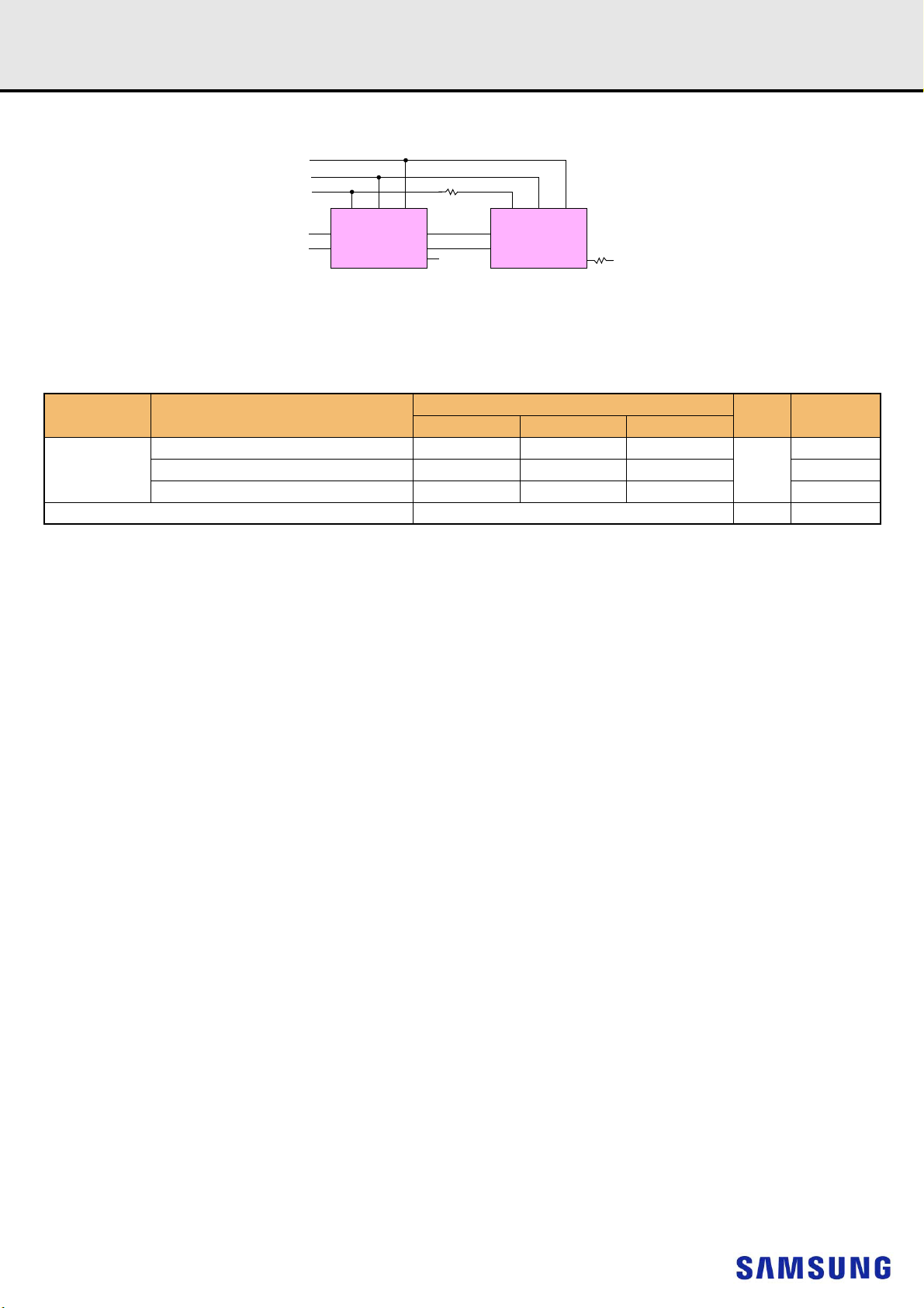
8. REGISTERING CLOCK DRIVER SPECIFICATION
8.1 Timing & Capacitance Values
Symbol Parameter Conditions
fclock Input Clock Frequency application frequency 625 1080 625 1350 TBD TBD MHz
t
CH/tCL
t
t
PDM
t
C
C
NOTE :
1) This parameter does not include package capacitance.
2) Data inputs are DCKE0/1, DODT0/1, DA0..DA17, DBA0..DBA1, DBG0..DBG1, DACT_n, DC0..DC2, DPAR, DCS0/1_n.
Pulse duration, CK_t, CK_c
HIGH or LOW
Inputs active time4 before
ACT
DRST_n is taken HIGH
Propagation delay, single-bit
switching, CK_t/ CK_c to output
output disable time
DIS
t
output enable time
EN
C
Input capacitance, Data inputs
I
Input capacitance, CK_t, CK_c
CK
Input capacitance, DRST_n
IR
DCKE0/1 = LOW and
DCS0/1_n = HIGH
1.2V Operation 1 1.3 1 1.3 TBD TBD ns
Rising edge of Yn_t to
output float
Output valid to rising
edge of Yn_t
1),2)
NOTE
1),2)
NOTE
or VSS;
V
I=VDD
=1.2V
V
DD
DDR4-1600/1866/2133 DDR4-2400/2666 DDR4-2933
Min Max Min Max Min Max
0.4 - 0.4 - TBD -
16 - 16 - TBD -
0.5*tCK +
tQSK1(min)
0.5*tCK -
tQSK1(max)
0.8 1.1 0.8 1.0 TBD TBD
0.8 1.1 0.8 1.0 TBD TBD
0.5 2.0 0.5 2.0 TBD TBD
-
-
0.5*tCK +
tQSK1(min)
0.5*tCK -
tQSK1(max)
-TBD-ps
-TBD-ps
Units
t
CK
t
CK
pF
8.2 Clock Driver Characteristics
Symbol Parameter Conditions
t
jit
t
STAB
t
t
jit
t
(hper)
jit
t
t
dynoff
(cc)
CKsk
(per)
Qsk1
Cycle-to-cycle period jitter CK_t/CK_c stable 0
Stabilization time - 5 - 5 - 5 - TBD us
Clock Output skew - 10 - 10 - 10 - TBD ps
Yn Clock Period jitter
Half period jitter
Qn Output to clock toler-
ance
Maximum re-driven
dynamic clock off-set
DDR4-1600/1866/
2133
Min Max Min Max Min Max Min Max
0.025 x
tCK
-0.025 *
tCK
-0.032 *
tCK
-0.125 *
tCK
0.025 *
tCK
0.032 *
tCK
0.125 *
tCK
-50-45-45-TBDps
DDR4-2400 DDR4-2666 DDR4-2933
0
-0.025 *
tCK
-0.032 *
tCK
-0.125 *
tCK
0.025 x
tCK
0.025 *
tCK
0.032 *
tCK
0.125 *
tCK
-0.025 *
tCK
-0.032 *
tCK
-0.1 * tCK 0.1 * tCK TBD TBD ps
0.025 x
0
tCK
0.025 *
tCK
0.032 *
tCK
TBD TBD ps
TBD TBD ps
TBD TBD ps
Units
- 11 -
Page 12
Rev. 1.3
DQS0_t
DQS0_c
DQ[7:0]
DQS_t
DQS_c
U1
CKE
ODT
ZQ
DQ[7:0]
CS_n
CS0A_n
ODT0A
CKE0A
VSS
DQS1_t
DQS1_c
DQ[15:8]
DQS_t
DQS_c
U2
CKE
ODT
ZQ
DQ[7:0]
CS_n
VSS
DQS2_t
DQS2_c
DQ[23:16]
DQS_t
DQS_c
U3
CKE
ODT
ZQ
DQ[7:0]
CS_n
VSS
DQS3_t
DQS3_c
DQ[31:24]
DQS_t
DQS_c
U4
CKE
ODT
ZQ
DQ[7:0]
CS_n
VSS
DQS8_t
DQS8_c
DQ[7:0]
DQS_t
DQS_c
U5
CKE
ODT
ZQ
DQ[7:0]
CS_n
VSS
DQS4_t
DQS4_c
DQ[39:32]
DQS_t
DQS_c
U6
CKE
ODT
ZQ
DQ[7:0]
CS_n
CS0B_n
ODT0B
CKE0B
VSS
DQS5_t
DQS5_c
DQ[47:40]
DQS_t
DQS_c
U7
CKE
ODT
ZQ
DQ[7:0]
CS_n
VSS
DQS6_t
DQS6_c
DQ[55:48]
DQS_t
DQS_c
U8
CKE
ODT
ZQ
DQ[7:0]
CS_n
VSS
DQS7_t
DQS7_c
DQ[63:56]
DQS_t
DQS_c
U9
CKE
ODT
ZQ
DQ[7:0]
CS_n
VSS
DQS0_t
DQS0_c
DQ[7:0]
DQS_t
DQS_c
U10
CKE
ODT
ZQ
DQ[7:0]
CS_n
CS1A_n
ODT1A
CKE1A
VSS
DQS1_t
DQS1_c
DQ[15:8]
DQS_t
DQS_c
U11
CKE
ODT
ZQ
DQ[7:0]
CS_n
VSS
DQS2_t
DQS2_c
DQ[23:16]
DQS_t
DQS_c
U12
CKE
ODT
ZQ
DQ[7:0]
CS_n
VSS
DQS3_t
DQS3_c
DQ[31:24]
DQS_t
DQS_c
U13
CKE
ODT
ZQ
DQ[7:0]
CS_n
VSS
DQS8_t
DQS8_c
DQ[7:0]
DQS_t
DQS_c
U14
CKE
ODT
ZQ
DQ[7:0]
CS_n
VSS
DQS4_t
DQS4_c
DQ[39:32]
DQS_t
DQS_c
U15
CKE
ODT
ZQ
DQ[7:0]
CS_n
CS1B_n
ODT1B
CKE1B
VSS
DQS5_t
DQS5_c
DQ[47:40]
DQS_t
DQS_c
U16
CKE
ODT
ZQ
DQ[7:0]
CS_n
VSS
DQS6_t
DQS6_c
DQ[55:48]
DQS_t
DQS_c
U17
CKE
ODT
ZQ
DQ[7:0]
CS_n
VSS
DQS7_t
DQS7_c
DQ[63:56]
DQS_t
DQS_c
U18
CKE
ODT
ZQ
DQ[7:0]
CS_n
VSS
datasheet
DDR4 SDRAMRegistered DIMM
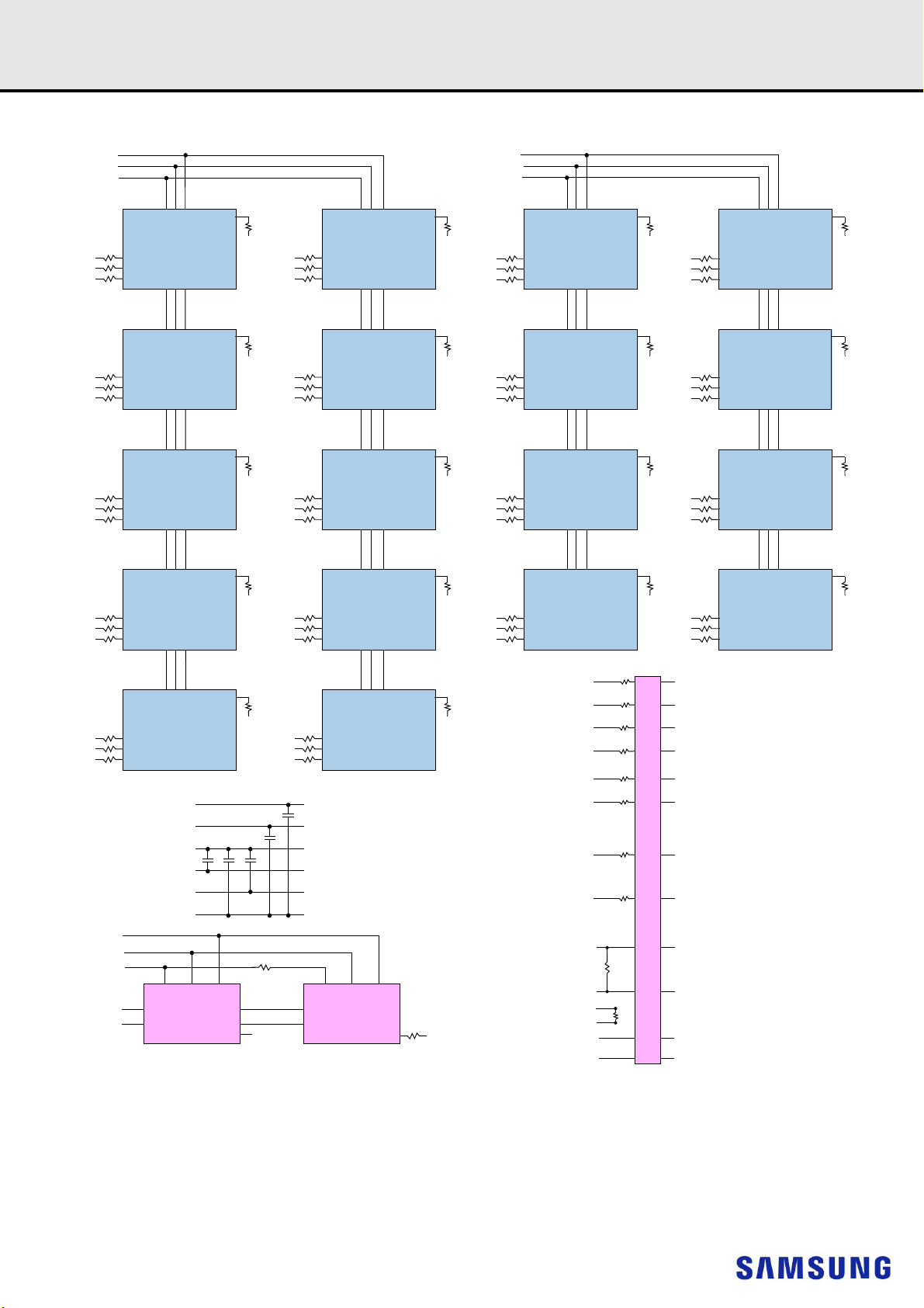
9. FUNCTION BLOCK DIAGRAM:
9.1 16GB, 2Gx72 Module (Populated as 2 rank of x8 DDR4 SDRAMs)
NOTE :
1) Unless otherwise noted, resistor values are 15 5%.
2) See the Net Structure diagrams for all resistors associated with the command, address and control bus.
3) ZQ resistors are 240 1%. For all other resistor values refer to the appropriate wiring diagram.
4) VDDSPD connects to the RCD and the SPD-TSE.
- 12 -
Page 13
Rev. 1.3
R
E
G
I
S
T
E
R
BA[1:0]
A[17:0]
ACT_n
PARITY
CKE0
RESET_n
BA[1:0]A -> BA[1:0]: SDRAMs U[5:1], U[14:10]
A[16:0]A -> A[16:0]: SDRAMs U[5:1], U[14:10]
ACTA_n -> ACT_n: SDRAMs U[5:1], U[14:10]
CKE0A -> CKE: SDRAMs U[5:1]
BG[1:0] BG[1:0]A -> BG[1:0] : SDRAMs
U[5:1], U[14:10]
BA[1:0]B -> BA[1:0]: SDRAMs U[9:6], U[18:15]
A[16:0]B -> A[16:0]: SDRAMs U[9:6], U[18:15]
ACTB_n -> ACT_n: SDRAMs U[9:6], U[18:15]
PARA -> PAR: SDRAMs U[5:1], U[14:10]
PARB -> PAR: SDRAMs U[9:6], U[18:U15]
CKE0B -> CKE: SDRAMs U[9:6]
Y0_c -> CK_c: SDRAMs U[9:6]
Y1_c -> CK_c: SDRAMs U[5:1]
QRST_n -> RESET_n: All SDRAM
CK0_c
ODT0
CK0_t
Y0_t -> CK_t: SDRAMs U[9:6]
Y1_t -> CK_t: SDRAMs U[5:1]
BG[1:0]B-> BG[1:0]: SDRAMs U[9:6], U[18:15]
CK1_c
CK1
_t
CS0_n
ALERT_n
ERROR_IN_n <- ALERT_n: All SDRAMs
ODT0A -> ODT: SDRAMs U[5:1]
ODT0B -> ODT: SDRAMs U[9:6]
CS0A_n -> CS_n: SDRAMs U[5:1]
CS0B_n -> CS_n: SDRAMs U[9:6]
V
SS
V
PP
U1 - U18
V
TT
V
DDSPD
Serial PD
V
DD
V
REFCA
SA0 SA1 SA2
SCL
EVENT_n EVENT_n
SCL
SDASDA
Serial PD with Thermal sensor
SA0 SA1 SA2
VSS
BFUNC
SCL
SDA
U1 - U18
U1 - U18
U1 - U18
SA0 SA1 SA2
SA1
SA2
SA0
1K
5%
RCD
CKE1A -> CKE: SDRAMs U[14:10]
CKE1B -> CKE: SDRAMs U[18:15]
ODT1A -> ODT: SDRAMs U[14:10
ODT1B -> ODT: SDRAMs U[18:15]
CS1A_n -> CS_n: SDRAMs U[14;10]
CS1B_n -> CS_n: SDRAMs U[18:15]
Y2_t -> CK_t: SDRAMs U[18:U15]
Y3_t -> CK_t: SDRAMs U[14:10]
Y2_c -> CK_c: SDRAMs U[18:U15]
Y3_c -> CK_c: SDRAMs U[14:10]
CKE1
ODT1
CS1_n
datasheet
DDR4 SDRAMRegistered DIMM
- 13 -
Page 14
Rev. 1.3
DQS0_t
DQS0_c
DQ[3:0]
DQS_t
DQS_c
D1
CKE
ODT
ZQ
DQ[3:0]
CS_n
DQS1_t
DQS1_c
DQ[11:8]
DQS_t
DQS_c
D2
CKE
ODT
ZQ
DQ[3:0]
CS_n
DQS2_t
DQS2_c
DQ[19:16]
DQS_t
DQS_c
D3
CKE
ODT
ZQ
DQ[3:0]
CS_n
DQS3_t
DQS3_c
DQ[27:24]
DQS_t
DQS_c
D4
CKE
ODT
ZQ
DQ[3:0]
CS_n
DQS8_t
DQS8_c
CB[3:0]
DQS_t
DQS_c
D5
CKE
ODT
ZQ
DQ[3:0]
CS_n
DQS_t
DQS_c
D6
CKE
ODT
ZQ
DQ[3:0]
CS_n
DQS_t
DQS_c
D7
CKE
ODT
ZQ
DQ[3:0]
CS_n
DQS_t
DQS_c
D8
CKE
ODT
ZQ
DQ[3:0]
CS_n
DQS_t
DQS_c
D9
CKE
ODT
ZQ
DQ[3:0]
CS_n
DQS_t
DQS_c
D10
CKE
ODT
ZQ
DQ[3:0]
CS_n
DQS_t
DQS_c
D15
CKE
ODT
ZQ
DQ[3:0]
CS_n
DQS_t
DQS_c
D16
CKE
ODT
ZQ
DQ[3:0]
CS_n
DQS_t
DQS_c
D17
CKE
ODT
ZQ
DQ[3:0]
CS_n
DQS_t
DQS_c
D18
CKE
ODT
ZQ
DQ[3:0]
CS_n
DQS4_t
DQS4_c
DQ[35:32]
DQS_t
DQS_c
D11
CKE
ODT
ZQ
DQ[3:0]
CS_n
DQS5_t
DQS5_c
DQ[43:40]
DQS_t
DQS_c
D12
CKE
ODT
ZQ
DQ[3:0]
CS_n
DQS6_t
DQS6_c
DQ[51:48]
DQS_t
DQS_c
D13
CKE
ODT
ZQ
DQ[3:0]
CS_n
DQS7_t
DQS7_c
DQ[59:56]
DQS_t
DQS_c
D14
CKE
ODT
ZQ
DQ[3:0]
CS_n
QACS0_n
QAODT0
QACKE0
QBCS0_n
QBODT0
QBCKE0
VSS VSS VSSVSSVSS
VSS VSS VSSVSSVSS
VSS VSSVSSVSS
VSS VSSVSSVSS
R
E
G
I
S
T
E
R
BA[1:0]
A[17:0]
ACT_n
PARITY
CKE0
RESET_n
QABA[1:0] -> BA[1:0] : SDRAMs D[10:1]
QAA[17:0] -> A[17:0] : SDRAMs D[10:1]
QAACT_n -> ACT_n : SDRAMs D[10:1]
QACKE0 -> CKE : SDRAMs D[10:1]
BG[1:0] QABG[1:0] -> BG[1:0] : SDRAMs D[10:1]
QBBA[1:0] -> BA[1:0] : SDRAMs D[18:11]
QBA[17:0] -> A[17:0] : SDRAMs D[18:11]
QBACT_n -> ACT_n : SDRAMs D[18:11]
QAPAR -> PAR : SDRAMs D[10:1]
QBPAR -> PAR : SDRAMs D[18:11]
QBCKE0 -> CKE : SDRAMs D[18:11]
Y0_c -> CK_c : SDRAMs D[18:11]
Y1_c -> CK_c : SDRAMs D[10:1]
QRST_n -> RESET_n : All SDRAMs
CK0_c
ODT0
CK0_t
Y0_t -> CK_t : SDRAMs D[18:11]
Y1
_t
-> CK_t : SDRAMs D[10:1]
QBBG[1:0] -> BG[1:0] : SDRAMs D[18:11]
CK1_c
CK1_t
CS0_n
ALERT_n
ERROR_IN_n -> ALERT_n : All SDRAMs
QAODT0 -> ODT : SDRAMs D[10:1]
QBODT0 -> ODT : SDRAMs D[18:11]
QACS0_n -> CS_n : SDRAMs D[10:1]
QBCS0_n -> CS_n : SDRAMs D[18:11]
V
SS
V
PP
D1 - D18
V
TT
V
DDSPD
Serial PD
V
DD
V
REFCA
Thermal sensor
SA0 SA1 SA2
SCL
1K
EVENT_nEVENT_n
SCL
SDASDA
Serial PD with
SA0 SA1 SA2
VSSZQCAL
SCL
SDA
Register
SA0
SA1
SA2
D1 - D18
D1 - D18
D1 - D18
DQS9_t
DQS9_c
DQ[7:4]
DQS10_t
DQS10_c
DQ[15:12]
DQS11_t
DQS11_c
DQ[23:20]
DQS12_t
DQS12_c
DQ[31:28]
DQS17_t
DQS17_c
CB[7:4]
DQS13_t
DQS13_c
DQ[39:36]
DQS14_t
DQS14_c
DQ[47:44]
DQS15_t
DQS15_c
DQ[55:52]
DQS16_t
DQS16_c
DQ[63:60]
datasheet
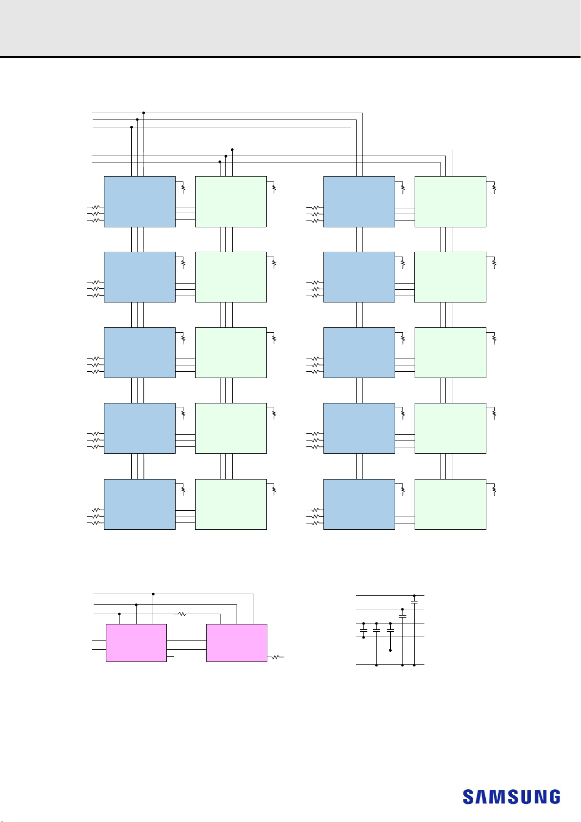
9.2 16GB, 2Gx72 Module (Populated as 1 rank of x4 DDR4 SDRAMs)
DDR4 SDRAMRegistered DIMM
NOTE :
1) Unless otherwise noted, resistor values are 15 5%.
2) See the Net Structure diagrams for all resistors associated with the command, address and control bus.
3) ZQ resistors are 240 1%. For all other resistor values refer to the appropriate wiring diagram.
- 14 -
Page 15
Rev. 1.3
DQS0_t
DQS0_c
DQ[3:0]
DQS_t
DQS_c
D6
CKE
ODT
ZQ
DQ[3:0]
CS
_n
DQS1_t
DQS1_c
DQ[11:8]
DQS_t
DQS_c
D7
CKE
ODT
ZQ
DQ[3:0]
CS
_n
DQS2_t
DQS2_c
DQ[19:16]
DQS_t
DQS_c
D8
CKE
ODT
ZQ
DQ[3:0]
CS
_n
DQS3_t
DQS3_c
DQ[27:24]
DQS_t
DQS_c
D9
CKE
ODT
ZQ
DQ[3:0]
CS
_n
DQS_t
DQS_c
D16
CKE
ODT
ZQ
DQ[3:0]
CS
_n
DQS_t
DQS_c
D17
CKE
ODT
ZQ
DQ[3:0]
CS
_n
DQS_t
DQS_c
D18
CKE
ODT
ZQ
DQ[3:0]
CS
_n
DQS_t
DQS_c
D19
CKE
ODT
ZQ
DQ[3:0]
CS
_n
DQS_t
DQS_c
D11
CKE
ODT
ZQ
DQ[3:0]
CS
_n
DQS_t
DQS_c
D12
CKE
ODT
ZQ
DQ[3:0]
CS
_n
DQS_t
DQS_c
D13
CKE
ODT
ZQ
DQ[3:0]
CS
_n
DQS_t
DQS_c
D14
CKE
ODT
ZQ
DQ[3:0]
CS
_n
DQS9_t
DQS9_c
DQ[7:4]
DQS_t
DQS_c
D1
CKE
ODT
ZQ
DQ[3:0]
CS
_n
DQS10_t
DQS10_c
DQ[15:12]
DQS_t
DQS_c
D2
CKE
ODT
ZQ
DQ[3:0]
CS
_n
DQS11_t
DQS11_c
DQ[23:20]
DQS_t
DQS_c
D3
CKE
ODT
ZQ
DQ[3:0]
CS
_n
DQS12_t
DQS12_c
DQ[31:28]
DQS_t
DQS_c
D4
CKE
ODT
ZQ
DQ[3:0]
CS
_n
QACS0
_n
QAODT0
QACKE0
VSS VSSVSSVSS
VSS VSSVSSVSS
VSS VSSVSSVSS
VSS VSSVSSVSS
Thermal sensor
SA0 SA1 SA2
SCL
1K
EVENT_nEVENT_n
SCL
SDASDA
Serial PD with
SA0 SA1 SA2
VSSZQCAL
SCL
SDA
Register
SA0
SA1
SA2
QACS1
_n
QAODT1
QACKE1
DQS8_t
DQS8_c
CB[3:0]
DQS_t
DQS_c
D10
CKE
ODT
ZQ
DQ[3:0]
CS
_n
DQS_t
DQS_c
D20
CKE
ODT
ZQ
DQ[3:0]
CS
_n
DQS_t
DQS_c
D15
CKE
ODT
ZQ
DQ[3:0]
CS
_n
DQS17_t
DQS17_c
CB[7:4]
DQS_t
DQS_c
D5
CKE
ODT
ZQ
DQ[3:0]
CS
_n
VSS
VSS
VSS
VSS
V
SS
V
PP
D1 - D36
V
TT
V
DDSPD
Serial PD
V
DD
V
REFCA
D1 - D36
D1 - D36
D1 - D36
datasheet
DDR4 SDRAMRegistered DIMM
9.3 32GB, 4Gx72 Module (Populated as 2 ranks of x4 DDR4 SDRAMs)
NOTE :
1) Unless otherwise noted, resistor values are 15 5%.
2) See the Net Structure diagrams for all resistors associated with the command, address and control bus.
3) ZQ resistors are 240 1%. For all other resistor values refer to the appropriate wiring diagram.
- 15 -
Page 16
Rev. 1.3
DQS4_t
DQS4_c
DQ[35:32]
DQS_t
DQS_c
D25
CKE
ODT
ZQ
DQ[3:0]
CS
_n
DQS5_t
DQS5_c
DQ[43:40]
DQS_t
DQS_c
D26
CKE
ODT
ZQ
DQ[3:0]
CS
_n
DQS6_t
DQS6_c
DQ[51:48]
DQS_t
DQS_c
D27
CKE
ODT
ZQ
DQ[3:0]
CS
_n
DQS7_t
DQS7_c
DQ[59:56]
DQS_t
DQS_c
D28
CKE
ODT
ZQ
DQ[3:0]
CS
_n
DQS_t
DQS_c
D33
CKE
ODT
ZQ
DQ[3:0]
CS
_n
DQS_t
DQS_c
D34
CKE
ODT
ZQ
DQ[3:0]
CS
_n
DQS_t
DQS_c
D35
CKE
ODT
ZQ
DQ[3:0]
CS
_n
DQS_t
DQS_c
D36
CKE
ODT
ZQ
DQ[3:0]
CS
_n
DQS_t
DQS_c
D29
CKE
ODT
ZQ
DQ[3:0]
CS
_n
DQS_t
DQS_c
D30
CKE
ODT
ZQ
DQ[3:0]
CS
_n
DQS_t
DQS_c
D31
CKE
ODT
ZQ
DQ[3:0]
CS
_n
DQS_t
DQS_c
D32
CKE
ODT
ZQ
DQ[3:0]
CS
_n
DQS13_t
DQS13_c
DQ[39:36]
DQS_t
DQS_c
D21
CKE
ODT
ZQ
DQ[3:0]
CS
_n
DQS14_t
DQS14_c
DQ[47:44]
DQS_t
DQS_c
D22
CKE
ODT
ZQ
DQ[3:0]
CS
_n
DQS15_t
DQS15_c
DQ[55:52]
DQS_t
DQS_c
D23
CKE
ODT
ZQ
DQ[3:0]
CS
_n
DQS16_t
DQS16_c
DQ[63:60]
DQS_t
DQS_c
D24
CKE
ODT
ZQ
DQ[3:0]
CS
_n
QBCS0_n
QBODT0
QBCKE0
VSS VSSVSSVSS
VSS VSSVSSVSS
VSS VSSVSSVSS
VSS VSSVSSVSS
QBCS1_n
QBODT1
QBCKE1
R
E
G
I
S
T
E
R
BA[1:0]
A[17:0]
ACT
_n
C[2:0]
PARITY
CKE0
CKE1
RESET
_n
QABA[1:0] -> BA[1:0] : SDRAMs D[20:1]
QAA[17:0] -> A[17:0] : SDRAMs D[20:1]
QAACT_n -> ACT_n : SDRAMs D[20:1]
QAC[2:0] -> C[2:0] : SDRAMs D[20:1]
QACKE0 -> CKE : SDRAMs D[10:1]
BG[1:0] QABG[1:0] -> BG[1:0] : SDRAMs D[20:1]
QBBA[1:0] -> BA[1:0] : SDRAMs D[36:21]
QBA[17:0] -> A[17:0] : SDRAMs D[36:21]
QBACT_n -> ACT_n : SDRAMs D[36:21]
QBC[2:0] -> C[2:0] : SDRAMs D[36:21]
QAPAR -> PAR : SDRAMs D[20:1]
QBPAR -> PAR : SDRAMs D[36:21]
QBCKE0 -> CKE : SDRAMs D[28:21]
Y0
_c
-> CK_c : SDRAMs D[24:21], D[32:29]
Y1
_c
-> CK_c: SDRAMs D[5:1], D[15:11]
QRST
_n
-> RESET_n : All SDRAMs
CK0
_c
ODT0
QACKE1 -> CKE : SDRAMs D[20:11]
QBCKE1 -> CKE : SDRAMs D[36:29]
CK0
_t
Y0_t -> CK_t : SDRAMs D[24:21], D[32:29]
Y1
_t
-> CK_t : SDRAMs D[5:1], D[15:11]
QBBG[1:0] -> BG[1:0] : SDRAMs D[36:21]
CK
1
_c
CK1
_t
ODT1
CS0
_n
CS1
_n
ALERT
_n
ERROR_IN_n - ALERT_n : All SDRAMs
QAODT0 -> ODT : SDRAMs D[10:1]
QBODT0 -> ODT : SDRAMs D[28:21]
QAODT1 -> ODT : SDRAMs D[20:11]
QBODT1 -> ODT : SDRAMs D[36:29]
QACS0_n -> CS_n : SDRAMs D[10:1]
QBCS0_n -> CS_n : SDRAMs D[28:21]
QACS1_n -> CS_n : SDRAMs D[20:11]
QBCS1_n -> CS_n : SDRAMs D[36:29]
Y2
_t
-> CK_t : SDRAMs D[28:25], D[36:33]
Y3
_t
-> CK_t : SDRAMs D[10:6], D[20:16]
Y2
_c
-> CK_c : SDRAMs D[28:25], D[36:33]
Y3
_c
-> CK_c : SDRAMs D[10:6], D[20:16]
datasheet
DDR4 SDRAMRegistered DIMM
NOTE :
CK0_t, CK0_c terminated with 120 ± 5% resistor
1)
2) CK1_t, CK1_c terminated with 120 ± 5% resistor but not used.
3) Unless otherwise noted resistors are 22 ± 5%.
.
- 16 -
Page 17
Rev. 1.3
Registered DIMM
datasheet
DDR4 SDRAM
10. ABSOLUTE MAXIMUM RATINGS
10.1 Absolute Maximum DC Ratings
[Table 5] Absolute Maximum DC Ratings
Symbol Parameter Rating Units NOTE
VDD Voltage on VDD pin relative to Vss -0.3 ~ 1.5 V 1,3
VDDQ Voltage on VDDQ pin relative to Vss -0.3 ~ 1.5 V 1,3
VPP Voltage on VPP pin relative to Vss -0.3 ~ 3.0 V 4
V
NOTE :
1) Stresses greater than those listed under “Absolute Maximum Ratings” may cause permanent damage to the device. This is a stress rating only and functional operation of the
device at these or any other conditions above those indicated in the operational sections of this specification is not implied. Exposure to absolute maximum rating conditions
for extended periods may affect reliability
2) Storage Temperature is the case surface temperature on the center/top side of the DRAM. For the measurement conditions, please refer to JESD51-2 standard.
3) VDD and VDDQ must be within 300mV of each other at all times; and VREFCA must be not greater than 0.6 x VDDQ, When VDD and VDDQ are less than 500mV; VREFCA
may be equal to or less than 300mV
4) VPP must be equal or greater than VDD/VDDQ at all times.
5) Overshoot area above 1.5 V is specified in section Address, Command and Control Overshoot and Undershoot specifications, Clock Overshoot and Undershoot
Specifications and section Data, Strobe and Mask Overshoot and Undershoot Specifications.
Voltage on any pin except VREFCA relative to Vss -0.3 ~ 1.5 V 1,3,5
IN, VOUT
T
Storage Temperature -55 to +100 °C 1,2
STG
11. AC & DC OPERATING CONDITIONS
[Table 6] Recommended DC Operating Conditions
Symbol Parameter
VDD Supply Voltage 1.14 1.2 1.26 V 1,2,3
VDDQ Supply Voltage for Output 1.14 1.2 1.26 V 1,2,3
VPP Peak-to-Peak Voltage 2.375 2.5 2.75 V 3
NOTE
:
1) Under all conditions V
tracks with VDD. AC parameters are measured with VDD and V
2) V
DDQ
3) DC bandwidth is limited to 20MHz.
must be less than or equal to VDD.
DDQ
Min. Typ. Max.
tied together.
DDQ
Rating
Unit NOTE
- 14 -
Page 18
Rev. 1.3
voltage
V
DD
V
SS
time
Registered DIMM
datasheet
DDR4 SDRAM
12. AC & DC INPUT MEASUREMENT LEVELS
12.1 AC & DC Logic Input Levels for Single-Ended Signals
[Table 7] Single-ended AC & DC Input Levels for Command and Address
Symbol Parameter
VIH.CA(DC75)
VIH.CA(DC65) - -
VIL.CA(DC75)
VIL.CA(DC65) - - VSS
VIH.CA(AC100)
VIH.CA(AC90) - -
VIL.CA(AC100)
VIL.CA(AC90) - - Note 2
VREFCA(DC) Reference Voltage for ADD, CMD inputs 0.49*VDD 0.51*VDD - - V 2,3
NOTE
:
1) See “Overshoot and Undershoot Specifications” on section.
2) The AC peak noise on VREFCA may not allow VREFCA to deviate from VREFCA(DC) by more than ± 1% VDD (for reference : approx. ± 12mV)
3) For reference : approx. VDD/2 ± 12mV.
DC input logic high
DC input logic low
AC input logic high
AC input logic low
DDR4-1600/1866/2133/2400 DDR4-2666/2933
Min. Max. Min. Max.
+ 0.075
V
REFCA
V
VSS
+ 0.1
REF
Note 2
VDD - -
V
+ 0.065
REFCA
V
-0.075
REFCA
Note 2 - -
V
- 0.1
REF
--
V
+ 0.09
REF
--
V
REFCA
V
VDD
Note 2
REF
-0.065
- 0.09
Unit NOTE
V
V
V
V
1
1
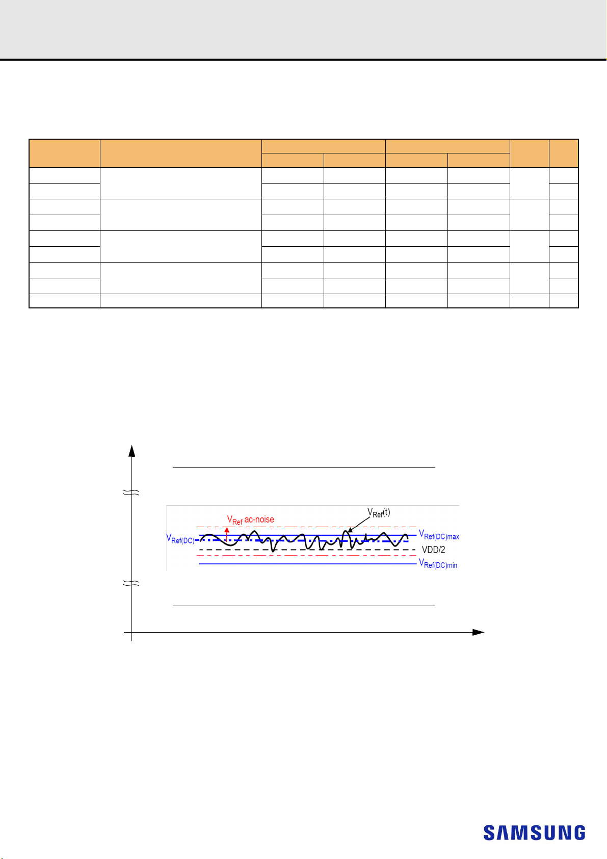
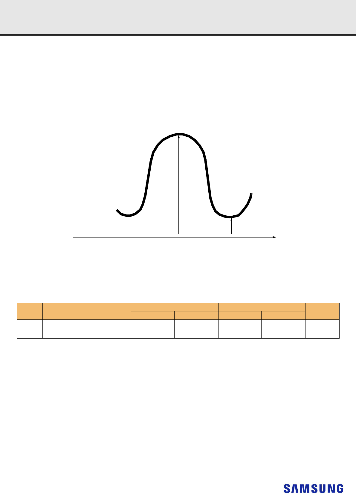
12.2 AC and DC Input Measurement Levels: V
The DC-tolerance limits and ac-noise limits for the reference voltages V
function of time. (V
V
(DC) is the linear average of V
REF
Furthermore V
The voltage levels for setup and hold time measurements VIH(AC), VIH(DC), VIL(AC) and VIL(DC) are dependent on V
stands for V
REF
(t) may temporarily deviate from V
REF
).
REFCA
(t) over a very long period of time (e.g. 1 sec). This average has to meet the min/max requirement in Table 7.
REF
(DC) by no more than ± 1% VDD.
REF
Figure 1. Illustration of V
(DC) tolerance and V
REF
is illustrated in Figure 1. It shows a valid reference voltage V
REFCA
Tolerances.
REF
AC-noise limits
REF
REF
(t) as a
REF
.
"V
" shall be understood as V
REF
This clarifies, that DC-variations of V
which setup and hold is measured. System timing and voltage budgets need to account for V
data-eye of the input signals.
This also clarifies that the DRAM setup/hold specification and derating values need to include time and voltage associated with V
and voltage effects due to AC-noise on V
(DC), as defined in Figure 1.
REF
affect the absolute voltage a signal has to reach to achieve a valid high or low level and therefore the time to
REF
(DC) deviations from the optimum position within the
REF
up to the specified limit (+/-1% of VDD) are included in DRAM timings and their associated deratings.
REF
- 15 -
AC-noise. Timing
REF
Page 19
Rev. 1.3
0.0
tDVAC
V
IH
.DIFF.MIN
half cycle
Differential Input Voltage (CK-CK)
time
tDVAC
VIH.DIFF.AC.MIN
V
IL
.DIFF.MAX
V
IL
.DIFF.AC.MAX
(CK_t - CK_c)
Registered DIMM
datasheet
12.3 AC and DC Logic Input Levels for Differential Signals
12.3.1 Differential Signals Definition
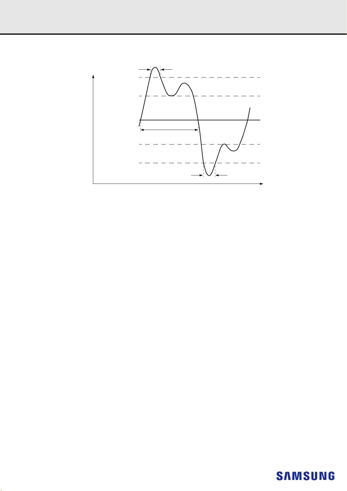
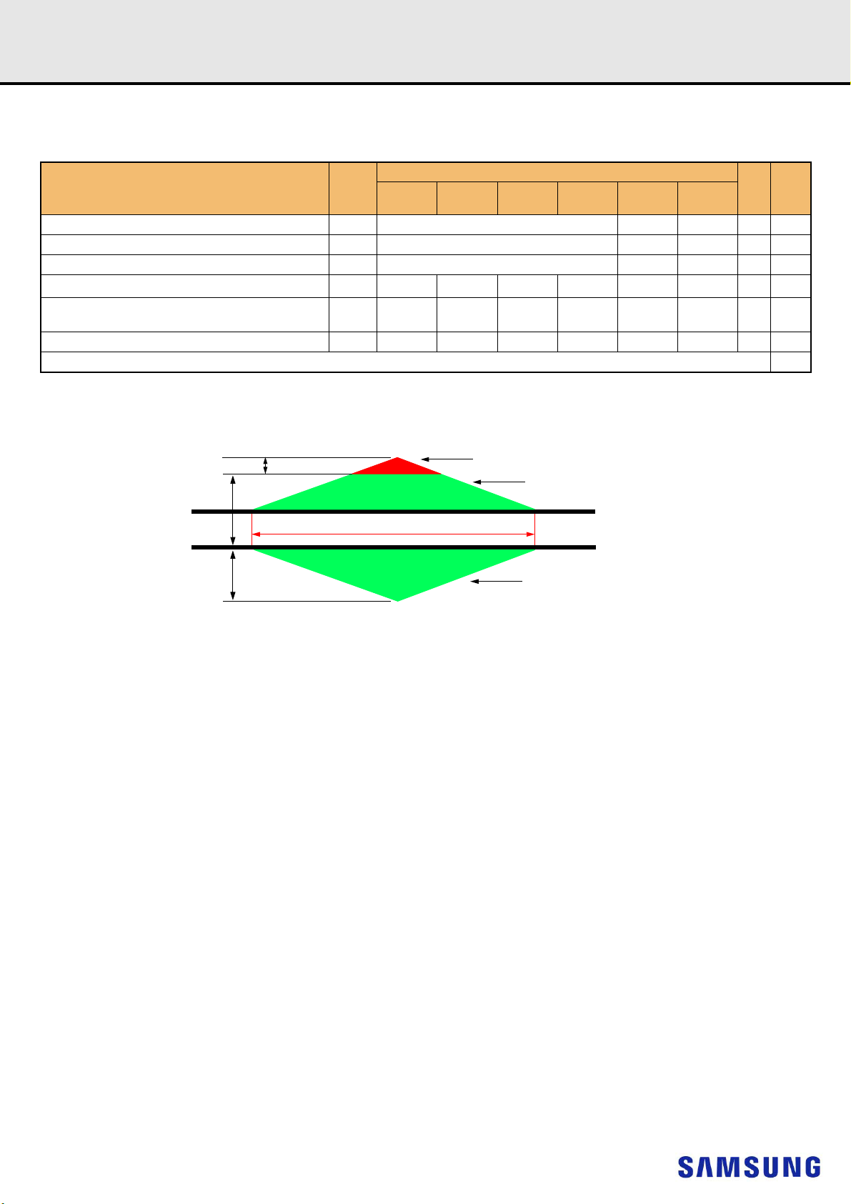
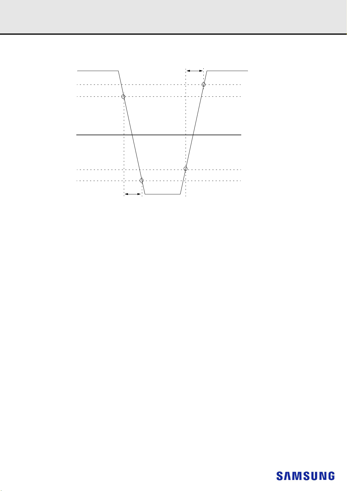
Figure 2. Definition of differential ac-swing and “time above ac-level” t
NOTE
:
1) Differential signal rising edge from VIL.DIFF.MAX to VIH.DIFF.MIN must be monotonic slope.
2) Differential signal falling edge from VIH.DIFF.MIN to VIL.DIFF.MAX must be monotonic slope.
DDR4 SDRAM
DVAC
- 16 -
Page 20
Rev. 1.3
Registered DIMM
datasheet
12.3.2 Differential Swing Requirements for Clock (CK_t - CK_c)
[Table 8] Differential AC and DC Input Levels
Symbol Parameter
V
IHdiff
V
ILdiff
V
(AC)
IHdiff
V
(AC)
ILdiff
NOTE :
1) Used to define a differential signal slew-rate.
2) for CK_t - CK_c use V
3) These values are not defined; however, the differential signals CK_t - CK_c, need to be within the respective limits (V
as well as the limitations for overshoot and undershoot.
[Table 9] Allowed Time Before Ringback (tDVAC) for CK_t - CK_c
differential input high +0.150 NOTE 3 TBD NOTE 3 V 1
differential input low NOTE 3 -0.150 NOTE 3 TBD V 1
differential input high ac
differential input low ac NOTE 3
IH.CA/VIL.CA
Slew Rate [V/ns]
> 4.0 120 -
4.0 115 -
3.0 110 -
2.0 105 -
1.8 100 -
1.6 95 -
1.4 90 -
1.2 85 -
1.0 80 -
< 1.0 80 -
(AC) of ADD/CMD and V
2 x (VIH(AC) - V
DDR4 -1600/1866/2133 DDR4 -2400/2666/2933
min max min max
REFCA
)
REF
;
min max
NOTE 3
2 x (VIL(AC) - V
tDVAC [ps] @ |V
2 x (VIH(AC) - V
)
REF
IH/Ldiff
REF
NOTE 3
(DC) max, V
IH.CA
(AC)| = 200mV
DDR4 SDRAM
unit NOTE
)
NOTE 3 V 2
2 x (VIL(AC) - V
(DC)min) for single-ended signals
IL.CA
REF
)
V2
- 17 -
Page 21
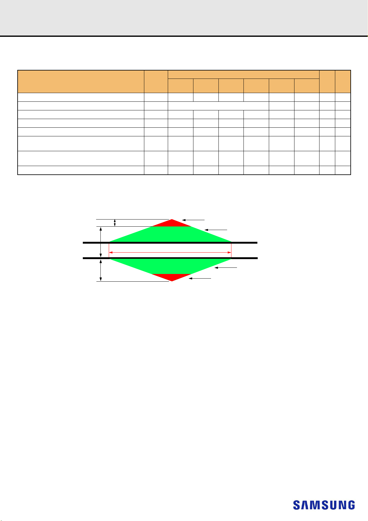
Rev. 1.3
VDD or V
DDQ
V
SEH
min
V
DD
/2 or V
DDQ
/2
V
SEL
max
V
SEH
VSS or V
SSQ
V
SEL
CK
time
Registered DIMM
datasheet
DDR4 SDRAM
12.3.3 Single-ended Requirements for Differential Signals
Each individual component of a differential signal (CK_t, CK_c) has also to comply with certain requirements for single-ended signals.
CK_t and CK_c have to approximately reach VSEHmin / VSELmax (approximately equal to the ac-levels (VIH.CA(AC) / VIL.CA(AC)) for ADD/CMD
signals) in every half-cycle.
Note that the applicable ac-levels for ADD/CMD might be different per speed-bin etc. E.g., if Different value than VIH.CA(AC100)/VIL.CA(AC100) is used
for ADD/CMD signals, then these ac-levels apply also for the single-ended signals CK_t and CK_c.
Figure 3. Single-ended requirement for differential signals.
Note that, while ADD/CMD signal requirements are with respect to VrefCA, the single-ended components of differential signals have a requirement with
respect to VDD / 2; this is nominally the same. The transition of single-ended signals through the ac-levels is used to measure setup time. For singleended components of differential signals the requirement to reach VSELmax, VSEHmin has no bearing on timing, but adds a restriction on the common
mode characteristics of these signals.
[Table 10] Single-ended Levels for CK_t, CK_c
Symbol Parameter
V
V
NOTE :
1) For CK_t - CK_c use V
2) V
IH
3) These values are not defined, however the single-ended signals CK_t - CK_c need to be within the respective limits (V
signals as well as the limitations for overshoot and undershoot.
Single-ended high-level for
SEH
Single-ended low-level for
SEL
(AC)/VIL(AC) for ADD/CMD is based on V
IH.CA/VIL.CA
(AC) of ADD/CMD;
CK_t, CK_c
CK_t, CK_c
;
REFCA
DDR4-1600/1866/2133 DDR4-2400/2666/2933
Min Max Min Max
(VDD/2)+0.100 NOTE3 TBD NOTE3 V 1, 2
NOTE3 (VDD/2)-0.100 NOTE3 TBD V 1, 2
(DC) max, V
IH.CA
IL.CA
Unit NOTE
(DC)min) for single-ended
- 18 -
Page 22

Rev. 1.3
A
AOS1
V
DD
A
AUS
V
SS
Volts
(V)
1 tCK
V
AOSP
A
AOS2
V
AOS
V
AUS
Registered DIMM
datasheet
DDR4 SDRAM
12.3.4 Address, Command and Control Overshoot and Undershoot specifications
[Table 11] AC overshoot/undershoot specification for Address, Command and Control pins
Parameter
Maximum peak amplitude above VAOS VAOSP 0.06 TBD TBD V
Upper boundary of overshoot area AAOS1 VAOS VDD +0.24 TBD TBD V 1
Maximum peak amplitude allowed for undershoot
Maximum overshoot area per 1 tCK above VAOS AAOS2 0.0083 0.0071 0.0062 0.0055 TBD TBD V-ns
Maximum overshoot area per 1 tCK between VDD and
VAOS
Maximum undershoot area per 1 tCK below VSS AAUS 0.2644 0.2265 0.1984 0.1762 TBD TBD V-ns
(A0-A13,A17,BG0-BG1,BA0-BA1,ACT_n,RAS_n/A16,CAS_n/A15,WE_n/A14,CS_n,CKE,ODT,C2-C0)
NOTE :
1) The value of VAOS matches VDD absolute max as defined in Table 5 Absolute Maximum DC Ratings if VDD equals VDD max as defined in Table 6 Recommended DC
Operating Conditions. If VDD is above the recommended operating conditions, VAOS remains at VDD absolute max as defined in Table 5.
Sym-
bol
VAUS 0.30 TBD TBD V
AAOS1 0.2550 0.2185 0.1914 0.1699 TBD TBD V-ns
DDR4-
1600
DDR4-
1866
Specification
DDR4-
2133
DDR4-
2400
DDR4-
2666
DDR4-
2933
Unit NOTE
Figure 4. Address, Command and Control Overshoot and Undershoot Definition
- 19 -
Page 23
Rev. 1.3
A
COS1
V
DD
A
CUS
V
SS
Volts
(V)
1 UI
V
COSP
A
COS2
V
COS
V
CUS
Registered DIMM
datasheet
DDR4 SDRAM
12.3.5 Clock Overshoot and Undershoot Specifications
[Table 12] AC overshoot/undershoot specification for Clock
Specification
Parameter Symbol
Maximum peak amplitude above VCOS VCOSP 0.06 TBD TBD V
Upper boundary of overshoot area ADOS1 VCOS VDD +0.24 TBD TBD V 1
Maximum peak amplitude allowed for undershoot VCUS 0.30 TBD TBD V
Maximum overshoot area per 1 UI above VCOS
Maximum overshoot area per 1 UI between VDD and
VDOS
Maximum undershoot area per 1 UI below VSS ACUS 0.1144 0.0980 0.0858 0.0762 TBD TBD V-ns
NOTE :
1) The value of VCOS matches VDD absolute max as defined in Table 5 Absolute Maximum DC Ratings if VDD equals VDD max as defined in Table 6 Recommended DC
Operating Conditions. If VDD is above the recommended operating conditions, VCOS remains at VDD absolute max as defined in Table 5.
ACOS2 0.0038 0.0032 0.0028 0.0025 TBD TBD V-ns
ACOS1 0.1125 0.0964 0.0844 0.0750 TBD TBD V-ns
DDR4-
1600
(CK_t, CK_c)
DDR4-
1866
DDR4-
2133
DDR4-
2400
DDR4-
2666
DDR4-
2933
Unit NOTE
Figure 5. Clock Overshoot and Undershoot Definition
- 20 -
Page 24
Rev. 1.3
A
DOS1
V
DDQ
A
DUS2
V
SSQ
Volts
(V)
1 UI
V
DOSP
A
DOS2
V
DOS
V
DUSP
A
DUS1
Registered DIMM
datasheet
DDR4 SDRAM
12.3.6 Data, Strobe and Mask Overshoot and Undershoot Specifications
[Table 13] AC overshoot/undershoot specification for Data, Strobe and Mask
Specification
Parameter Symbol
Maximum peak amplitude above VDOS VDOSP 0.16 0.16 0.16 0.16 TBD TBD V
Upper boundary of overshoot area ADOS1 VDOS VDDQ + 0.24 TBD TBD V 1
Lower boundary of undershoot area ADUS1 VDUS 0.30 0.30 0.30 0.30 TBD TBD V 2
Maximum peak amplitude below VDUS VDUSP 0.10 0.10 0.10 0.10 TBD TBD V
Maximum overshoot area per 1 UI above VDOS ADOS2 0.0150 0.0129 0.0113 0.0100 TBD TBD V-ns
Maximum overshoot area per 1 UI between
VDDQ and VDOS
Maximum undershoot area per 1 UI between
VSSQ and VDUS1
Maximum undershoot area per 1 UI below VDUS ADUS2 0.0150 0.0129 0.0113 0.0100 TBD TBD V-ns
NOTE
:
1) The value of VDOS matches (VIN, VOUT) max as defined in Table 5 Absolute Maximum DC Ratings if VDDQ equals VDDQ max as defined in Table 6 Recommended DC
Operating Conditions. If VDDQ is above the recommended operating conditions, VDOS remains at (VIN, VOUT) max as defined in Table 5.
2) The value of VDUS matches (VIN, VOUT) min as defined in Table 5 Absolute Maximum DC Ratings
ADOS1 0.1050 0.0900 0.0788 0.0700 TBD TBD V-ns
ADUS1 0.1050 0.0900 0.0788 0.0700 TBD TBD V-ns
DDR4-
1600
DDR4-
1866
DDR4-
2133
DDR4-
2400
DDR4-
2666
DDR4-
2933
Unit
NOT
E
Figure 6. Data, Strobe and Mask Overshoot and Undershoot Definition
- 21 -
Page 25
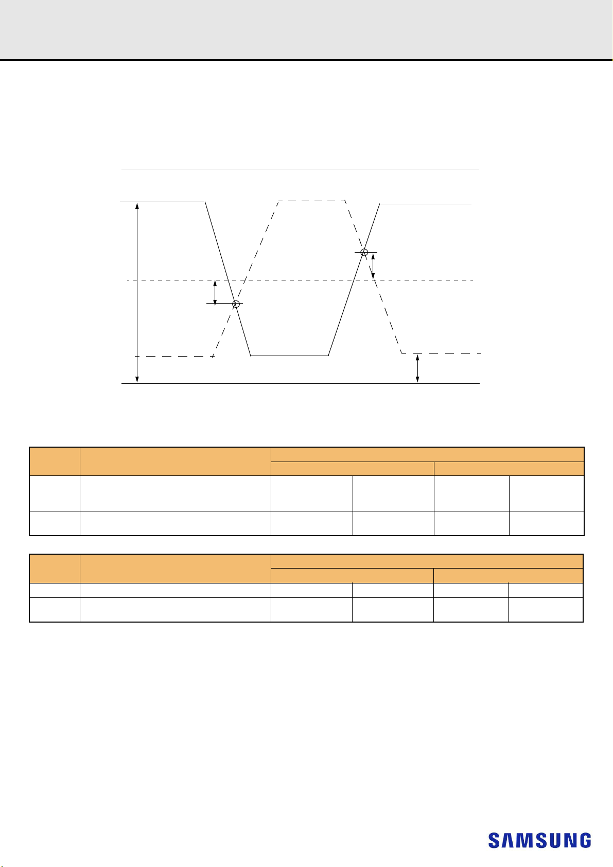
Rev. 1.3
Delta TRdiff
Delta TFdiff
V
IHdiffmin
0
V
ILdiffmax
Differential Input Voltage(i,e, CK_t - CK_c)
Registered DIMM
datasheet
12.4 Slew Rate Definitions
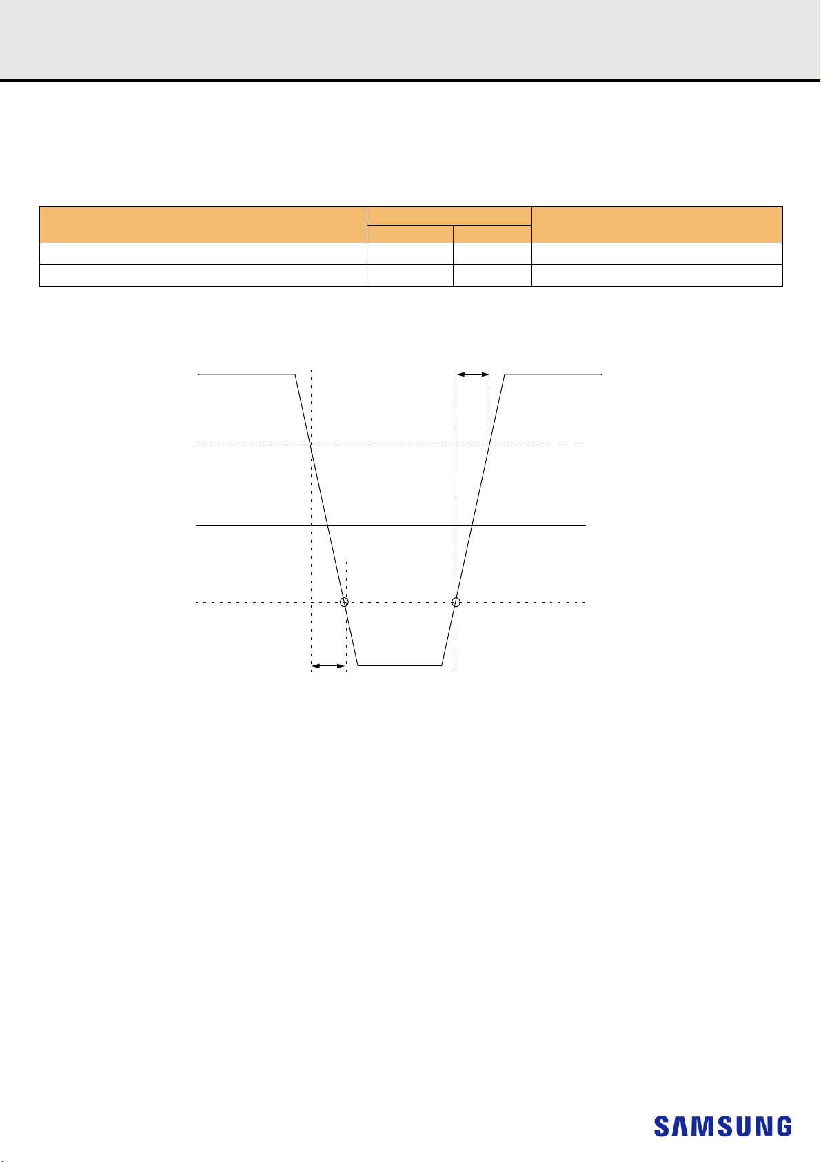
12.4.1 Slew Rate Definitions for Differential Input Signals (CK)
Input slew rate for differential signals (CK_t, CK_c) are defined and measured as shown in Table 14 and Figure 7.
[Table 14] Differential Input Slew Rate Definition
Description
Differential input slew rate for rising edge (CK_t - CK_c)
Differential input slew rate for falling edge (CK_t - CK_c)
NOTE :
1) The differential signal (i,e.,CK_t - CK_c) must be linear between these thresholds.
Measured
from to
V
ILdiffmax
V
IHdiffmin
V
IHdiffmin
V
ILdiffmax
[V
[V
DDR4 SDRAM
Defined by
IHdiffmin
IHdiffmin
- V
- V
ILdiffmax
ILdiffmax
] / DeltaTRdiff
] / DeltaTFdiff
Figure 7. Differential Input Slew Rate Definition for CK_t, CK_c
- 22 -
Page 26
Rev. 1.3
Delta TRsingle
Delta TFsingle
V
IHCA(AC) Min
V
IHCA(DC) Min
VREFCA(DC)
V
ILCA(DC) Max
V
ILCA(AC) Max
Registered DIMM
datasheet
12.4.2 Slew Rate Definition for Single-ended Input Signals (CMD/ADD)
DDR4 SDRAM
Figure 8. Single-ended Input Slew Rate definition for CMD and ADD
NOTE :
1) Single-ended input slew rate for rising edge = {VIHCA(AC)Min - VILCA(DC)Max} / Delta TR single.
2) Single-ended input slew rate for falling edge = {VIHCA(DC)Min - VILCA(AC)Max} / Delta TF single.
3) Single-ended signal rising edge from VILCA(DC)Max to VIHCA(DC)Min must be monotonic slope.
4) Single-ended signal falling edge from VIHCA(DC)Min to VILCA(DC)Max must be monotonic slope.
- 23 -
Page 27
Rev. 1.3
Vix
CK_t
VDD/2
VSS
VDD
CK_c
Vix
VSEL
VSEH
Registered DIMM
datasheet
DDR4 SDRAM
12.5 Differential Input Cross Point Voltage
To guarantee tight setup and hold times as well as output skew parameters with respect to clock, each cross point voltage of differential input signals
(CK_t, CK_c) must meet the requirements in Table 15. The differential input cross point voltage VIX is measured from the actual cross point of true and
complement signals to the midlevel between of VDD and VSS.
Figure 9. Vix Definition (CK)
[Table 15] Cross Point Voltage for Differential Input Signals (CK)
Symbol Parameter
- Area of VSEH, VSEL
VlX(CK)
Symbol Parameter
VlX(CK)
Differential Input Cross Point Voltage relative to
VDD/2 for CK_t, CK_c
- Area of VSEH, VSEL TBD TBD TBD TBD
Differential Input Cross Point Voltage relative to
VDD/2 for CK_t, CK_c
VSEL =< VDD/2 -
145mV
-120mV
TBD TBD TBD TBD
min max
min max
DDR4-1600/1866/2133
VDD/2 - 145mV =<
VSEL =< VDD/2 -
100mV
-(VDD/2 - VSEL) +
25mV
DDR4-2400/2666/2933
VDD/2 + 100mV =<
VSEH =< VDD/2 +
145mV
(VSEH - VDD/2) -
25mV
VDD/2 + 145mV =<
VSEH
120mV
- 24 -
Page 28

Rev. 1.3
0.8*VDD
TR_RESET
tPW_RESET
0.7*VDD
0.3*VDD
0.2*VDD
Registered DIMM
datasheet
DDR4 SDRAM
12.6 CMOS rail to rail Input Levels
12.6.1 CMOS rail to rail Input Levels for RESET_n
[Table 16] CMOS rail to rail Input Levels for RESET_n
Parameter Symbol Min Max Unit NOTE
AC Input High Voltage VIH(AC)_RESET 0.8*VDD VDD V 6
DC Input High Voltage VIH(DC)_RESET 0.7*VDD VDD V 2
DC Input Low Voltage VIL(DC)_RESET VSS 0.3*VDD V 1
AC Input Low Voltage VIL(AC)_RESET VSS 0.2*VDD V 7
Rising time TR_RESET - 1.0 us 4
RESET pulse width tPW_RESET 1.0 - us 3,5
NOTE :
1) After RESET_n is registered LOW, RESET_n level shall be maintained below VIL(DC)_RESET during tPW_RESET, otherwise, SDRAM may not be reset.
2) Once RESET_n is registered HIGH, RESET_n level must be maintained above VIH(DC)_RESET, otherwise, SDRAM operation will not be guaranteed until it is reset
asserting RESET_n signal LOW.
3) RESET is destructive to data contents.
4) No slope reversal(ringback) requirement during its level transition from Low to High.
5) This definition is applied only “Reset Procedure at Power Stable”.
6) Overshoot might occur. It should be limited by the Absolute Maximum DC Ratings.
7) Undershoot might occur. It should be limited by Absolute Maximum DC Ratings.
Figure 10. RESET_n Input Slew Rate Definition
- 25 -
Page 29

Rev. 1.3
Registered DIMM
datasheet
12.7 AC and DC Logic Input Levels for DQS Signals
12.7.1 Differential signal definition
DDR4 SDRAM
Figure 11. Definition of differential DQS Signal AC-swing Level
12.7.2 Differential swing requirements for DQS (DQS_t - DQS_c)
[Table 17] Differential AC and DC Input Levels for DQS
Symbol Parameter
VIHDiffPeak VIH.DIFF.Peak Voltage 186 Note2 160 Note2 TBD TBD mV 1
VILDiffPeak VIL.DIFF.Peak Voltage Note2 -186 Note2 -160 TBD TBD mV 1
NOTE :
1) Used to define a differential signal slew-rate.
2) These values are not defined; however, the differential signals DQS_t - DQS_c, need to be within the respective limits Overshoot, Undershoot Specification for single-ended
signals.
DDR4-1600, 1866, 2133 DDR4-2400 DDR4-2666, 2933
Min Max Min Max Min Max
Unit Note
- 26 -
Page 30

Rev. 1.3
DQS_t
DQS_c
Single Ended Input Voltage : DQS_t and DQS_c
Min(f(t))
+35%
+35%
+50%
+50%
Time
Max(f(t))
Registered DIMM
datasheet
DDR4 SDRAM
12.7.3 Peak voltage calculation method
The peak voltage of Differential DQS signals are calculated in a following equation.
VIH.DIFF.Peak Voltage = Max(f(t))
VIL.DIFF.Peak Voltage = Min(f(t))
f(t) = VDQS_t - VDQS_c
The Max(f(t)) or Min(f(t)) used to determine the midpoint which to reference the +/-35% window of the exempt non-monotonic signaling shall be the smallest peak voltage observed in all ui’s.
Figure 12. Definition of differential DQS Peak Voltage and rage of exempt non-monotonic signaling
- 27 -
Page 31

Rev. 1.3
C
D
B
A
VIX_DQS,RF
VIX_DQS,FR
VIX_DQS,FR
VIX_DQS,RF
DQS_t
VDQSmid
DQS_c
Lowest horizontal tangent above VDQSmid of the transitioning signals
DQS_t,DQS_c : Single-ended Input Voltages
V
SSQ
Highest horizontal tanget below VDQSmid of the transitioning signals
VDQS_trans/2
VDQS_trans
Registered DIMM
datasheet
DDR4 SDRAM
12.7.4 Differential Input Cross Point Voltage
To achieve tight RxMask input requirements as well as output skew parameters with respect to strobe, the cross point voltage of differential input signals
(DQS_t, DQS_c) must meet the requirements in Table 18. The differential input cross point voltage VIX_DQS (VIX_DQS_FR and VIX_DQS_RF) is
measured from the actual cross point of DQS_t, DQS_c relative to the VDQSmid of the DQS_t and DQS_c signals.
VDQSmid is the midpoint of the minimum levels achieved by the transitioning DQS_t and DQS_c signals, and noted by VDQS_trans. VDQS_trans is the
difference between the lowest horizontal tangent above VDQSmid of the transitioning DQS signals and the highest horizontal tangent below VDQSmid of
the transitioning DQS signals.
A non-monotonic transitioning signal’s ledge is exempt or not used in determination of a horizontal tangent provided the said ledge occurs within +/- 35%
of the midpoint of either VIH.DIFF.Peak Voltage (DQS_t rising) or VIL.DIFF.Peak Voltage (DQS_c rising), refer to Figure 12. A secondary horizontal tangent resulting from a ring-back transition is also exempt in determination of a horizontal tangent. That is, a falling transition’s horizontal tangent is derived
from its negative slope to zero slope transition (point A in Figure 13) and a ring-back’s horizontal tangent derived from its positive slope to zero slope transition (point B in Figure 13) is not a valid horizontal tangent; and a rising transition’s horizontal tangent is derived from its positive slope to zero slope transition (point C in Figure 13) and a ring-back’s horizontal tangent derived from its negative slope to zero slope transition (point D in Figure 13) is not a valid
horizontal tangent
Figure 13. Vix Definition (DQS)
[Table 18] Cross point voltage for DQS differential input signals
Symbol Parameter
Vix_DQS_ratio
VDQSmid_to_Vcent VDQSmid offset relative to Vcent_DQ(midpoint) -
NOTE :
1) Vix_DQS_Ratio is DQS VIX crossing (Vix_DQS_FR or Vix_DQS_RF) divided by VDQS_trans. VDQS_trans is the difference between the lowest horizontal tangent above
VDQSmid of the transitioning DQS signals and the highest horizontal tangent below VDQSmid of the transitioning DQS signals.
2) VDQSmid will be similar to the VREFDQ internal setting value obtained during Vref Training if the DQS and DQs drivers and paths are matched.
3) The maximum limit shall not exceed the smaller of VIHdiff minimum limit or 50mV.
4) VIX measurements are only applicable for transitioning DQS_t and DQS_c signals when toggling data, preamble and high-z states are not applicable conditions.
5) The parameter VDQSmid is defined for simulation and ATE testing purposes, it is not expected to be tested in a system.
DQS_t and DQS_c crossing relative to the midpoint of
the DQS_t and DQS_c signal swings
DDR4-1600/1866/2133/ DDR4-2666, 2933
Min Max Min Max
- 25 - 25 % 1, 2
min
(VIHdiff,50)
-
min
(VIHdiff,50)
Unit Note
mV 3, 4, 5
- 28 -
Page 32
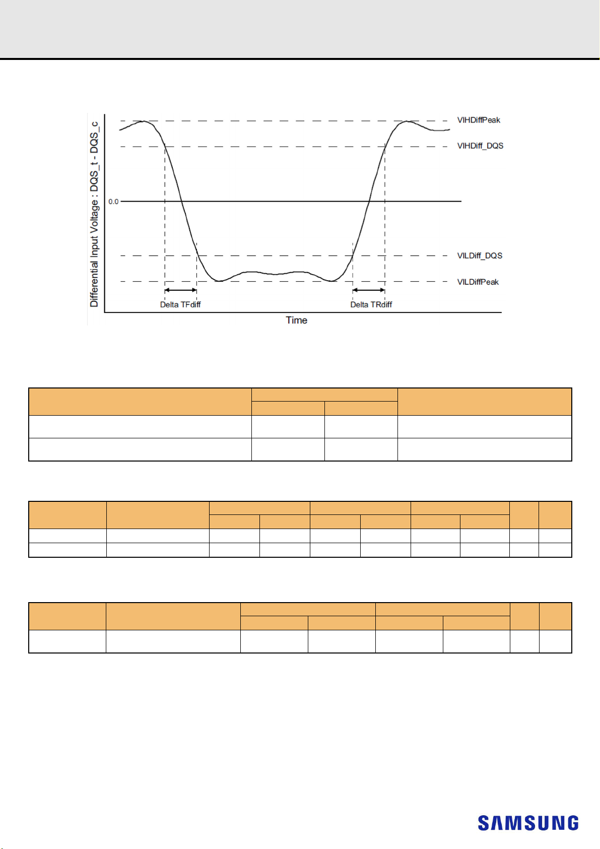
Rev. 1.3
Registered DIMM
datasheet
12.7.5 Differential Input Slew Rate Definition
Input slew rate for differential signals (DQS_t, DQS_c) are defined and measured as shown in Figure 13 and Figure 14.
NOTE :
1) Differential signal rising edge from VILDiff_DQS to VIHDiff_DQS must be monotonic slope.
2) Differential signal falling edge from VIHDiff_DQS to VILDiff_DQS must be monotonic slope.
Figure 14. Differential Input Slew Rate Definition for DQS_t, DQS_c
DDR4 SDRAM
[Table 19] Differential Input Slew Rate Definition for DQS_t, DQS_c
Description
Differential input slew rate for rising edge (DQS_t - DQS_c) VILDiff_DQS VIHDiff_DQS |VILDiff_DQS - VIHDiff_DQS|/DeltaTRdiff
Differential input slew rate for falling edge (DQS_t - DQS_c) VIHDiff_DQS VILDiff_DQS |VILDiff_DQS - VIHDiff_DQS|/DeltaTFdiff
[Table 20] Differential Input Level for DQS_t, DQS_c
Symbol Parameter
VIHDiff_DQS Differential Input High 136 - 130 - TBD TBD mV
VILDiff_DQS Differential Input Low - -136 - -130 TBD TBD mV
[Table 21] Differential Input Slew Rate for DQS_t, DQS_c
Symbol Parameter
SRIdiff Differential Input Slew Rate 3 18 TBD TBD V/ns
DDR4-1600/1866/2133 DDR4-2400 DDR4-2666, 2933
Min Max Min Max Min Max
DDR4-1600/1866/2133/2400 DDR4-2666, 2933
Min Max Min Max
Measured
From To
Defined by
Unit NOTE
Unit NOTE
- 29 -
Page 33
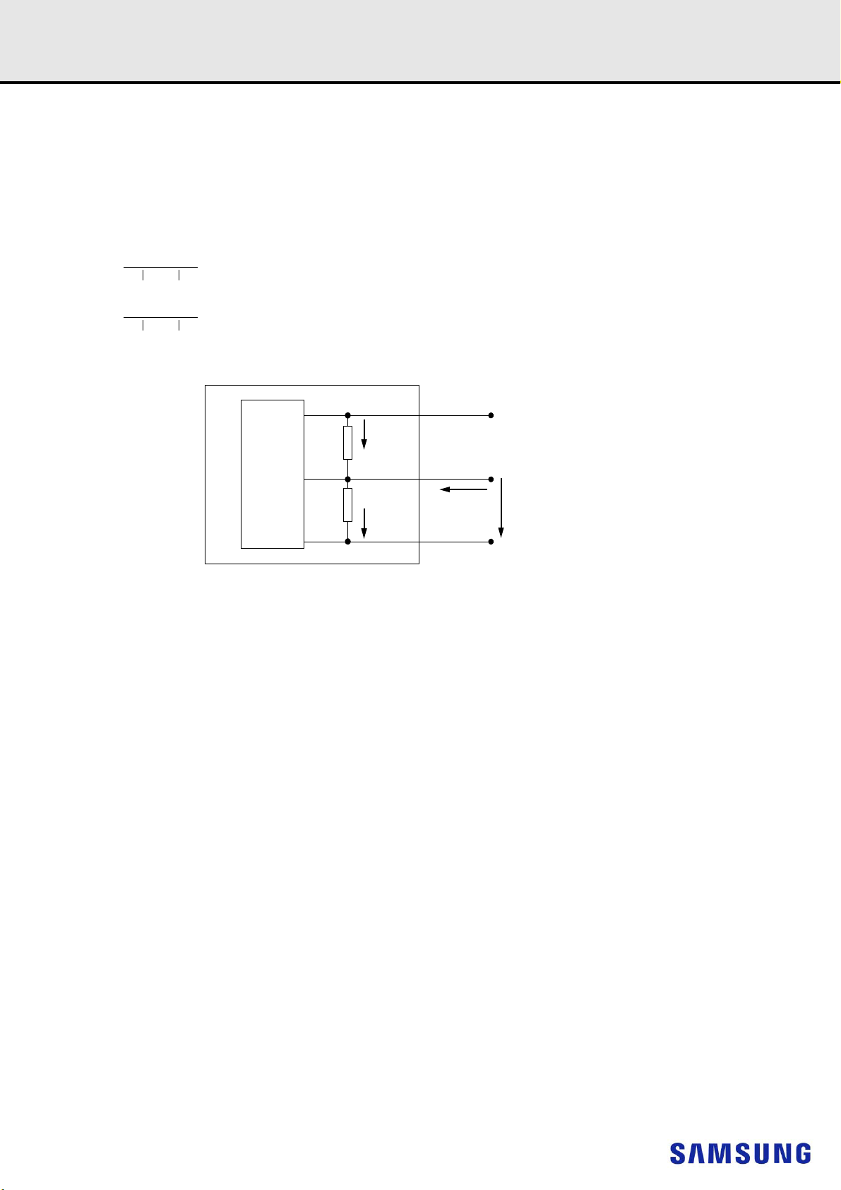
Rev. 1.3
RONPu =
VDDQ -Vout
I out
under the condition that RON
Pd
is off
RON
Pd
=
Vout
I out
under the condition that RON
Pu
is off
To
other
circuity
like
RCV, ...
Output Drive
DQ
RON
Pu
VSSQ
VDDQ
I
out
V
out
Chip In Drive Mode
RON
Pd
I
Pu
I
Pd
Registered DIMM
datasheet
DDR4 SDRAM
13. AC and DC output Measurement levels
13.1 Output Driver DC Electrical Characteristics
The DDR4 driver supports two different Ron values. These Ron values are referred as strong(low Ron) and weak mode(high Ron). A functional
representation of the output buffer is shown in the figure below. Output driver impedance RON is defined as follows:
The individual pull-up and pull-down resistors (RON
and RONPd) are defined as follows:
Pu
Figure 15. Output driver
- 30 -
Page 34
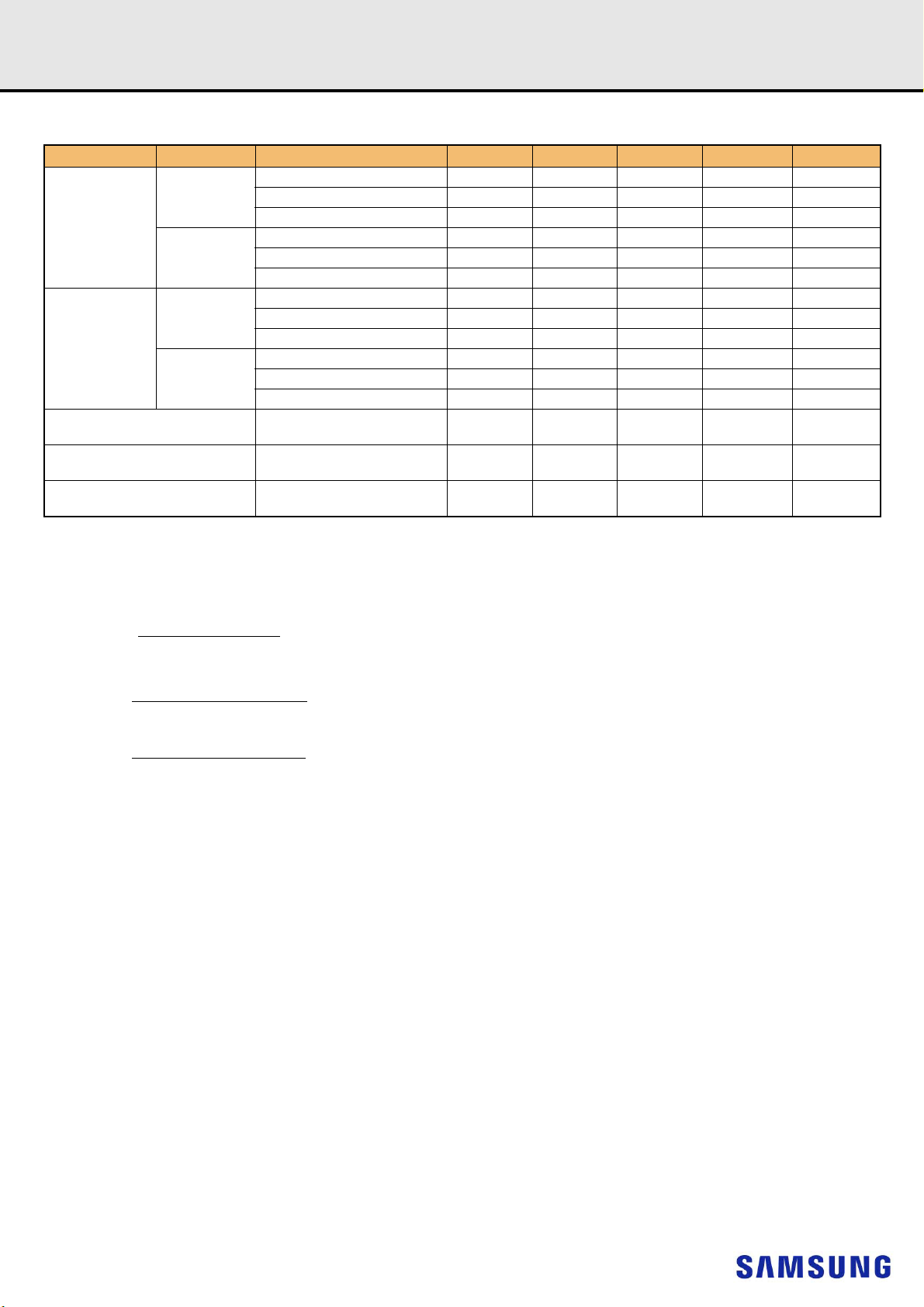
Rev. 1.3
MMPuPd =
RONPu -RONPd
RONNOM
*100
MMPudd =
RONPuMax -RONPuMin
RONNOM
*100
MMPddd =
RONPdMax -RONPdMin
RONNOM
*100
Registered DIMM
[Table 22] Output Driver DC Electrical Characteristics, assuming RZQ=240ohm; entire operating temperature range; after proper ZQ calibration
Mismatch between pull-up and
Mismatch DQ-DQ within byte vari-
Mismatch DQ-DQ within byte vari-
NOTE :
1) The tolerance limits are specified after calibration with stable voltage and temperature. For the behavior of the tolerance limits if temperature or voltage changes after calibration, see following section on voltage and temperature sensitivity (TBD).
2) Pull-up and pull-dn output driver impedances are recommended to be calibrated at 0.8 * VDDQ. Other calibration schemes may be used to achieve the linearity spec shown
above, e.g. calibration at 0.5 * VDDQ and 1.1 * VDDQ.
3) Measurement definition for mismatch between pull-up and pull-down, MMPuPd : Measure RONPu and RONPD both at 0.8*VDD separately; Ronnom is the nominal Ron
value
RON
NOM
34
48
pull-down, MMPuPd
ation pull-up, MMPudd
ation pull-dn, MMPddd
Resistor Vout Min Nom Max Unit NOTE
VOLdc= 0.5*VDDQ 0.8 1 1.1 RZQ/7 1,2
RON34Pd
RON34Pu
RON48Pd
RON48Pu
VOMdc= 0.8* VDDQ 0.9 1 1.1 RZQ/7 1,2
VOHdc= 1.1* VDDQ 0.9 1 1.25 RZQ/7 1,2
VOLdc= 0.5* VDDQ 0.9 1 1.25 RZQ/7 1,2
VOMdc= 0.8* VDDQ 0.9 1 1.1 RZQ/7 1,2
VOHdc= 1.1* VDDQ 0.8 1 1.1 RZQ/7 1,2
VOLdc= 0.5*VDDQ 0.8 1 1.1 RZQ/5 1,2
VOMdc= 0.8* VDDQ 0.9 1 1.1 RZQ/5 1,2
VOHdc= 1.1* VDDQ 0.9 1 1.25 RZQ/5 1,2
VOLdc= 0.5* VDDQ 0.9 1 1.25 RZQ/5 1,2
VOMdc= 0.8* VDDQ 0.9 1 1.1 RZQ/5 1,2
VOHdc= 1.1* VDDQ 0.8 1 1.1 RZQ/5 1,2
VOMdc= 0.8* VDDQ -10 - 10 % 1,2,3,4
VOMdc= 0.8* VDDQ - - 10 % 1,2,4
VOMdc= 0.8* VDDQ - - 10 % 1,2,4
datasheet
DDR4 SDRAM
4) RON variance range ratio to RON Nominal value in a given component, including DQS_t and DQS_c.
5) This parameter of x16 device is specified for Uper byte and Lower byte.
- 31 -
Page 35

Rev. 1.3
RONPd =
Vout
l Iout l
under the condition that RONPu is off
DRAM
Alert
VSSQ
I
out
V
out
RON
Pd
I
Pd
Alert Driver
Registered DIMM
datasheet
DDR4 SDRAM
13.1.1 Alert_n output Drive Characteristic
A functional representation of the output buffer is shown in the figure below. Output driver impedance RON is defined as follows:
Resistor Vout Min Max Unit NOTE
VOLdc= 0.1* VDDQ 0.3 1.2 34 1
= 0.8* VDDQ
RON
Pd
NOTE:
1) VDDQ voltage is at VDDQ DC. VDDQ DC definition is TBD.
V
V
OMdc
OHdc
= 1.1* VDDQ
0.4 1.2 34 1
0.4 1.4 34 1
- 32 -
Page 36

Rev. 1.3
RON
Pu_CT
=
V
DDQ-VOUT
l Iout l
RON
Pd_CT
=
V
OUT
l Iout l
V
DDQ
DQ
V
SSQ
RON
Pu_CT
I
Pd_CT
RON
Pd_CT
To
other
circuity
like
RCV,...
Output Driver
I
Pu_CT
Iout
Vout
Chip In Driver Mode
Registered DIMM
datasheet
13.1.2 Output Driver Characteristic of Connectivity Test (CT) Mode
Following Output driver impedance RON will be applied Test Output Pin during Connectivity Test (CT) Mode.
The individual pull-up and pull-down resistors (RONPu_CT and RONPd_CT) are defined as follows:
DDR4 SDRAM
Figure 16. Output Driver
RON
NOM_CT
34
NOTE :
1) Connectivity test mode uses un-calibrated drivers, showing the full range over PVT. No mismatch between pull up and pull down is defined
Resistor Vout Max Units NOTE
RON
RON
Pd_CT
Pu_CT
VOBdc = 0.2 x V
VOL
= 0.5 x V
dc
VOM
= 0.8 x V
dc
VOH
= 1.1 x V
dc
VOBdc = 0.2 x V
VOL
= 0.5 x V
dc
VOM
= 0.8 x V
dc
VOH
= 1.1 x V
dc
DDQ
DDQ
DDQ
DDQ
DDQ
DDQ
DDQ
DDQ
1.9 34 1
2.0 34 1
2.2 34 1
2.5 34 1
2.5 34 1
2.2 34 1
2.0 34 1
1.9 34 1
.
- 33 -
Page 37
Rev. 1.3
Registered DIMM
datasheet
DDR4 SDRAM
13.2 Single-ended AC & DC Output Levels
[Table 23] Single-ended AC & DC Output Levels
Symbol Parameter DDR4-1600/1866/2133/2400/2666/2933 Units NOTE
(DC)
V
OH
V
OM
V
OL
V
OH
V
OL
NOTE
1) The swing of ± 0.15 × V
load of 50
DC output high measurement level (for IV curve linearity)
(DC)
DC output mid measurement level (for IV curve linearity)
(DC)
DC output low measurement level (for IV curve linearity)
(AC)
AC output high measurement level (for output SR)
(AC)
AC output low measurement level (for output SR)
:
to VTT = V
is based on approximately 50% of the static single-ended output peak-to-peak swing with a driver impedance of RZQ/7 and an effective test
DDQ
.
DDQ
1.1 x V
DDQ
0.8 x V
DDQ
0.5 x V
DDQ
(0.7 + 0.15) x V
(0.7 - 0.15) x V
DDQ
DDQ
V
V
V
V1
V1
13.3 Differential AC & DC Output Levels
[Table 24] Differential AC & DC Output Levels
Symbol Parameter DDR4-1600/1866/2133/2400/2666/2933 Units NOTE
(AC)
V
OHdiff
V
(AC)
OLdiff
NOTE
:
1) The swing of ± 0.3 × V
to VTT = V
of 50
AC differential output high measurement level (for output SR)
AC differential output low measurement level (for output SR)
DDQ
is based on approximately 50% of the static differential output peak-to-peak swing with a driver impedance of RZQ/7 and an effective test load
DDQ
at each of the differential outputs.
+0.3 x V
-0.3 x V
DDQ
DDQ
V1
V1
- 34 -
Page 38
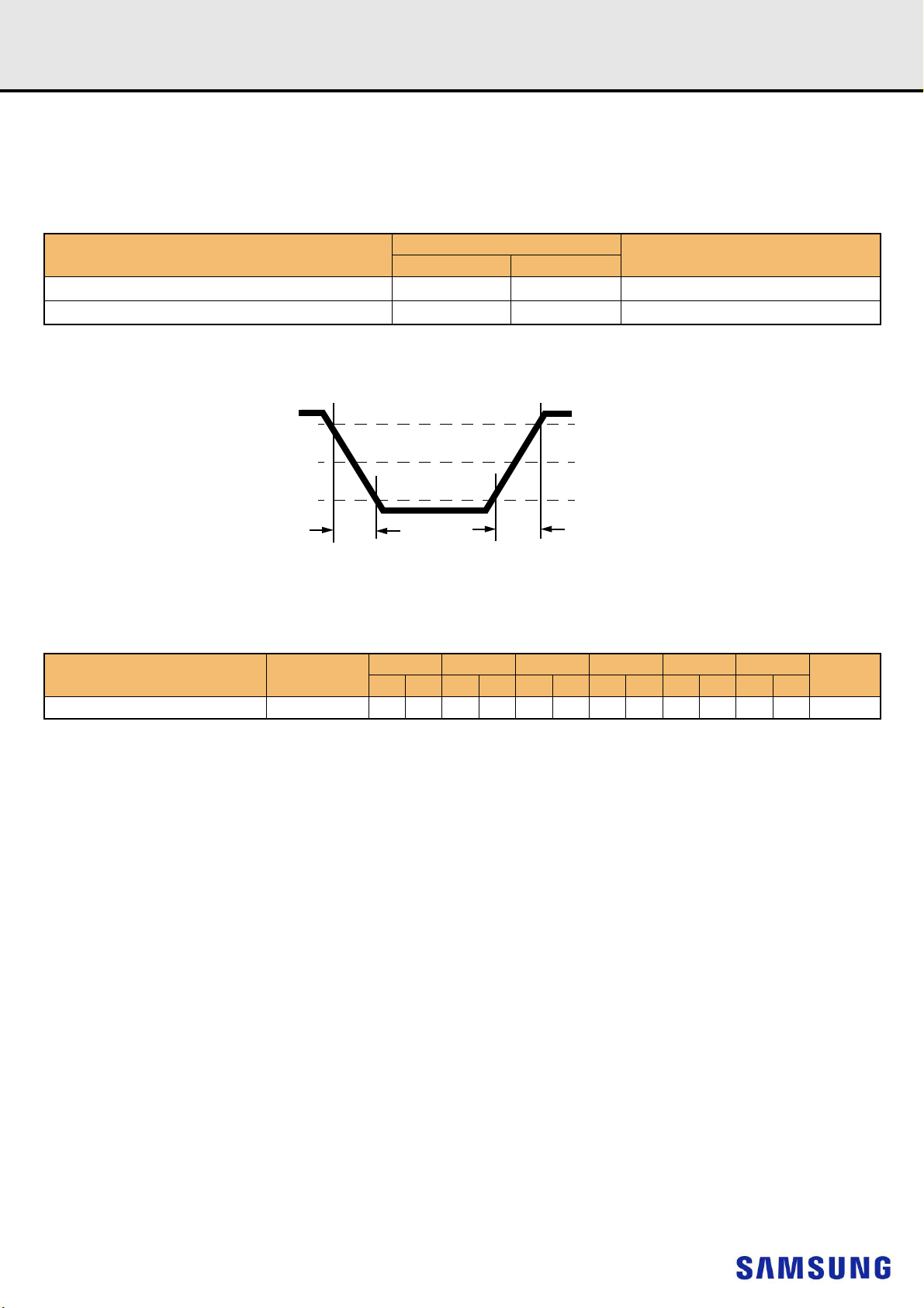
Rev. 1.3
V
OH(AC)
V
OL(AC)
delta
TRse
delta
TFse
VTT
Registered DIMM
datasheet
DDR4 SDRAM
13.4 Single-ended Output Slew Rate
With the reference load for timing measurements, output slew rate for falling and rising edges is defined and measured between V
single ended signals as shown in Table 25 and Figure 17.
[Table 25] Single-ended Output Slew Rate Definition
Description
Single ended output slew rate for rising edge
Single ended output slew rate for falling edge
NOTE
:
1) Output slew rate is verified by design and characterization, and may not be subject to production test.
V
V
Measured
From To
(AC) VOH(AC) [VOH(AC)-VOL(AC)] / Delta TRse
OL
(AC) VOL(AC) [VOH(AC)-VOL(AC)] / Delta TFse
OH
Defined by
OL(AC)
and V
OH(AC)
for
Figure 17. Single-ended Output Slew Rate Definition
[Table 26] Single-ended Output Slew Rate
Parameter Symbol
Single ended output slew rate SRQse 4 9 4 9 4 9 4 9 4 9 4 9 V/ns
Description: SR: Slew Rate
Q: Query Output (like in DQ, which stands for Data-in, Query-Output)
se: Single-ended Signals
For Ron = RZQ/7 setting
NOTE :
1) In two cases, a maximum slew rate of 12 V/ns applies for a single DQ signal within a byte lane.
-Case 1 is defined for a single DQ signal within a byte lane which is switching into a certain direction (either from high to low or low to high) while all remaining DQ signals in the
same byte lane are static (i.e. they stay at either high or low).
-Case 2 is defined for a single DQ signal within a byte lane which is switching into a certain direction (either from high to low or low to high) while all remaining DQ signals in the
same byte lane are switching into the opposite direction (i.e. from low to high or high to low respectively). For the remaining DQ signal switching into the opposite direction, the
regular maximum limit of 9 V/ns applies
DDR4-1600 DDR4-1866 DDR4-2133 DDR4-2400 DDR4-2666 DDR4-2933
Min Max Min Max Min Max Min Max Min Max Min Max
Units
- 35 -
Page 39

Rev. 1.3
V
OHdiff
(AC)
V
OLdiff
(AC)
delta
TRdiff
delta
TFdiff
VTT
Registered DIMM
datasheet
DDR4 SDRAM
13.5 Differential Output Slew Rate
With the reference load for timing measurements, output slew rate for falling and rising edges is defined and measured between VOLdiff(AC) and
VOHdiff(AC) for differential signals as shown in Table 27 and Figure 18.
[Table 27] Differential Output Slew Rate Definition
Description
Differential output slew rate for rising edge
Differential output slew rate for falling edge
NOTE
:
1) Output slew rate is verified by design and characterization, and may not be subject to production test.
V
V
OLdiff
OHdiff
Measured
From To
(AC) V
(AC) V
OHdiff
OLdiff
(AC) [V
(AC) [V
OHdiff
OHdiff
(AC)-V
(AC)-V
Defined by
(AC)] / Delta TRdiff
OLdiff
(AC)] / Delta TFdiff
OLdiff
Figure 18. Differential Output Slew Rate Definition
[Table 28] Differential Output Slew Rate
Parameter Symbol
Differential output slew rate SRQdiff 8 18 8 18 8 18 8 18 8 18 8 18 V/ns
Description:
SR: Slew Rate
Q: Query Output (like in DQ, which stands for Data-in, Query-Output)
diff: Differential Signals
For Ron = RZQ/7 setting
DDR4-1600 DDR4-1866 DDR4-2133 DDR4-2400 DDR4-2666 DDR4-2933
Min Max Min Max Min Max Min Max Min Max Min Max
Units
- 36 -
Page 40
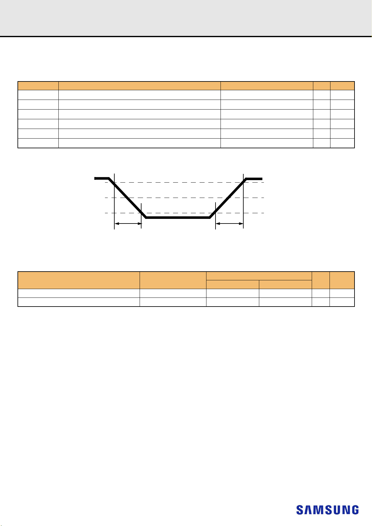
Rev. 1.3
VOH(AC)
TR_output_CT
VTT
VOL(AC)
TF_output_CT
0.5 * VDDQ
Registered DIMM
datasheet
DDR4 SDRAM
13.6 Single-ended AC & DC Output Levels of Connectivity Test Mode
Following output parameters will be applied for DDR4 SDRAM Output Signal during Connectivity Test Mode.
[Table 29] Single-ended AC & DC Output Levels of Connectivity Test Mode
Symbol Parameter DDR4-1600/1866/2133/2400/2666/2933 Unit Notes
V
OH(DC)
V
OM(DC)
V
OL(DC)
V
OB(DC)
V
OH(AC)
V
OL(AC)
NOTE :
1) The effective test load is 50 terminated by VTT = 0.5 * VDDQ.
DC output high measurement level (for IV curve linearity)
DC output mid measurement level (for IV curve linearity) 0.8 x VDDQ V
DC output low measurement level (for IV curve linearity) 0.5 x VDDQ V
DC output below measurement level (for IV curve linearity) 0.2 x VDDQ V
AC output high measurement level (for output SR) VTT + (0.1 x VDDQ) V 1
AC output below measurement level (for output SR) VTT - (0.1 x VDDQ) V 1
1.1 x VDDQ V
Figure 19. Output Slew Rate Definition of Connectivity Test Mode
[Table 30] Single-ended Output Slew Rate of Connectivity Test Mode
Parameter Symbol
Output signal Falling time TF_output_CT - 10 ns/V
Output signal Rising time TR_output_CT - 10 ns/V
DDR4-1600/1866/2133/2400/2666/2933
Min Max
Unit Notes
- 37 -
Page 41
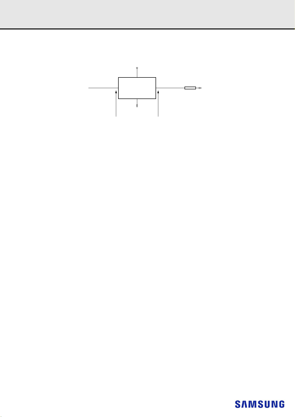
Rev. 1.3
V
DDQ
CT_INPUTS
DUT
DQ, DM
DQSU_t, DQSU_c
DQS_t, DQS_c
Rterm = 50 ohm
Timing Reference Points
V
SSQ
DQSL_t, DQSL_c
0.5*VDDQ
Registered DIMM
datasheet
13.7 Test Load for Connectivity Test Mode Timing
The reference load for ODT timings is defined in Figure 20.
Figure 20. Connectivity Test Mode Timing Reference Load
DDR4 SDRAM
- 38 -
Page 42

Rev. 1.3
datasheet
14. IDD SPEC TABLE
IDD and IPP values are for typical operating range of voltage and temperature unless otherwise noted.
[Table 31] IDD and I
Symbol
I
I
DD0A
I
I
DD1A
I
DD2N
I
DD2NA
I
DD2NT
I
DD2NL
I
DD2NG
I
DD2ND
I
DD2N_par
I
DD2P
I
DD2Q
I
DD3N
I
DD3NA
I
DD3P
I
DD4R
I
DD4RA
I
DD4RB
I
DD4W
I
DD4WA
I
DD4WB
I
DD4WC
I
DD4W_par
I
DD5B
I
DD5F2
I
DD5F4
I
DD6N
I
DD6E
I
DD6R
I
DD6A
I
I
NOTE :
1) DIMM IDD SPEC is based on the condition that de-actived rank (IDLE) is IDD2N. Please refer to Table .
2) IDD current measure method and detail patterns are described on DDR4 component datasheet.
3) VDD and VDDQ are merged on module PCB (IDDQ values are not considered by Qoff condition)
4) DIMM IDD Values are calculated based on the component IDD spec and Register power.
Specification for M393A2K43CB1
DDQ
DD0
DD1
DD7
DD8
M393A2K43CB1: 2Rx8
16GB(2Gx72) Module
DDR4-2400
17-17-17
VDD 1.2V VPP 2.5V
IDD Max. IPP Max.
738 63 mA
738 63 mA
890 63 mA
848 63 mA
667 54 mA
610 54 mA
610 54 mA
499 54 mA
640 54 mA
608 54 mA
683 54 mA
423 54 mA
648 54 mA
807 72 mA
827 72 mA
539 72 mA
118 0 63 m A
1200 63 mA
1235 63 mA
1202 54 mA
1254 54 mA
119 2 5 4 mA
1089 54 mA
1275 54 mA
2269 189 mA
1770 162 mA
1572 153 mA
389 72 mA
555 90 mA
276 72 mA
373 90 mA
1753 117 mA
150 54 mA
DDR4 SDRAMRegistered DIMM
Unit
- 42 -
Page 43

Rev. 1.3
datasheet
[Table 32] IDD and I
Symbol
I
DD0
I
DD0A
I
DD1
I
DD1A
I
DD2N
I
DD2NA
I
DD2NT
I
DD2NL
I
DD2NG
I
DD2ND
I
DD2N_par
I
DD2P
I
DD2Q
I
DD3N
I
DD3NA
I
DD3P
I
DD4R
I
DD4RA
I
DD4RB
I
DD4W
I
DD4WA
I
DD4WB
I
DD4WC
I
DD4W_par
I
DD5B
I
DD5F2
I
DD5F4
I
DD6N
I
DD6E
I
DD6R
I
DD6A
I
DD7
I
DD8
NOTE :
1) DIMM IDD SPEC is based on the condition that de-actived rank (IDLE) is IDD2N. Please refer to Table .
2) IDD current measure method and detail patterns are described on DDR4 component datasheet.
3) VDD and VDDQ are merged on module PCB (IDDQ values are not considered by Qoff condition)
4) DIMM IDD Values are calculated based on the component IDD spec and Register power.
Specification for M393A2K43CB2
DDQ
DDR4-2666 DDR4-2933
19-19-19 21-21-21
VDD 1.2V VPP 2.5V VDD 1.2V VPP 2.5V
IDD Max. IPP Max. IDD Max. IPP Max.
766 63 TBD TBD mA
792 63 TBD TBD mA
908 63 TBD TBD mA
961 63 TBD TBD mA
680 54 TBD TBD mA
731 54 TBD TBD mA
731 54 TBD TBD mA
582 54 TBD TBD mA
680 54 TBD TBD mA
645 54 TBD TBD mA
696 54 TBD TBD mA
431 54 TBD TBD mA
661 54 TBD TBD mA
823 72 TBD TBD mA
857 72 TBD TBD mA
549 72 TBD TBD mA
1488 63 TBD TBD mA
1540 63 TBD TBD mA
1499 63 TBD TBD mA
1414 54 TBD TBD mA
1459 54 TBD TBD mA
1423 54 TBD TBD mA
1356 54 TBD TBD mA
1513 54 TBD TBD mA
2315 189 TBD TBD mA
1806 162 TBD TBD mA
1604 153 TBD TBD mA
396 72 TBD TBD mA
589 90 TBD TBD mA
295 72 TBD TBD mA
391 90 TBD TBD mA
1923 126 TBD TBD mA
168 54 TBD TBD mA
M393A2K43CB2: 2Rx8
16GB(2Gx72) Module
DDR4 SDRAMRegistered DIMM
Unit
- 43 -
Page 44

Rev. 1.3
datasheet
[Table 33] IDD and I
Symbol
I
I
DD0A
I
I
DD1A
I
DD2N
I
DD2NA
I
DD2NT
I
DD2NL
I
DD2NG
I
DD2ND
I
DD2N_par
I
DD2P
I
DD2Q
I
DD3N
I
DD3NA
I
DD3P
I
DD4R
I
DD4RA
I
DD4RB
I
DD4W
I
DD4WA
I
DD4WB
I
DD4WC
I
DD4W_par
I
DD5B
I
DD5F2
I
DD5F4
I
DD6N
I
DD6E
I
DD6R
I
DD6A
I
I
NOTE :
1) DIMM IDD SPEC is based on the condition that de-actived rank (IDLE) is IDD2N. Please refer to Table .
2) IDD current measure method and detail patterns are described on DDR4 component datasheet.
3) VDD and VDDQ are merged on module PCB (IDDQ values are not considered by Qoff condition)
4) DIMM IDD Values are calculated based on the component IDD spec and Register power.
Specification for M393A2K40CB1
DDQ
DD0
DD1
DD7
DD8
M393A2K40CB1: 1Rx4
16GB(2Gx72) Module
DDR4-2400
17-17-17
VDD 1.2V VPP 2.5V
IDD Max. IPP Max.
805 72 mA
860 72 mA
980 72 mA
999 72 mA
676 54 mA
730 54 mA
730 54 mA
577 54 mA
678 54 mA
643 54 mA
694 54 mA
427 54 mA
659 54 mA
794 72 mA
829 72 mA
545 72 mA
1475 72 mA
1526 72 mA
1476 72 mA
1613 54 mA
1710 54 mA
1631 54 mA
1564 54 mA
1780 54 mA
4061 378 mA
2974 270 mA
2587 252 mA
420 72 mA
600 90 mA
301 72 mA
400 90 mA
2951 198 mA
196 54 mA
DDR4 SDRAMRegistered DIMM
Unit
- 44 -
Page 45

Rev. 1.3
datasheet
[Table 34] IDD and I
Symbol
I
DD0
I
DD0A
I
DD1
I
DD1A
I
DD2N
I
DD2NA
I
DD2NT
I
DD2NL
I
DD2NG
I
DD2ND
I
DD2N_par
I
DD2P
I
DD2Q
I
DD3N
I
DD3NA
I
DD3P
I
DD4R
I
DD4RA
I
DD4RB
I
DD4W
I
DD4WA
I
DD4WB
I
DD4WC
I
DD4W_par
I
DD5B
I
DD5F2
I
DD5F4
I
DD6N
I
DD6E
I
DD6R
I
DD6A
I
DD7
I
DD8
NOTE :
1) DIMM IDD SPEC is based on the condition that de-actived rank (IDLE) is IDD2N. Please refer to Table .
2) IDD current measure method and detail patterns are described on DDR4 component datasheet.
3) VDD and VDDQ are merged on module PCB (IDDQ values are not considered by Qoff condition)
4) DIMM IDD Values are calculated based on the component IDD spec and Register power.
Specification for M393A2K40CB2
DDQ
DDR4-2666 DDR4-2933
19-19-19 21-21-21
VDD 1.2V VPP 2.5V VDD 1.2V VPP 2.5V
IDD Max. IPP Max. IDD Max. IPP Max.
838 72 TBD TBD mA
891 72 TBD TBD mA
1000 72 TBD TBD mA
1102 72 TBD TBD mA
689 54 TBD TBD mA
744 54 TBD TBD mA
744 54 TBD TBD mA
588 54 TBD TBD mA
691 54 TBD TBD mA
656 54 TBD TBD mA
708 54 TBD TBD mA
435 54 TBD TBD mA
672 54 TBD TBD mA
810 72 TBD TBD mA
845 72 TBD TBD mA
556 72 TBD TBD mA
1937 72 TBD TBD mA
2043 72 TBD TBD mA
1938 72 TBD TBD mA
1908 54 TBD TBD mA
1999 54 TBD TBD mA
1925 54 TBD TBD mA
1806 54 TBD TBD mA
2120 54 TBD TBD mA
4143 378 TBD TBD mA
3034 270 TBD TBD mA
2639 252 TBD TBD mA
428 72 TBD TBD mA
612 72 TBD TBD mA
307 72 TBD TBD mA
408 72 TBD TBD mA
3470 216 TBD TBD mA
200 54 TBD TBD mA
M393A2K40CB2: 1Rx4
16GB(2Gx72) Module
DDR4 SDRAMRegistered DIMM
Unit
- 45 -
Page 46

Rev. 1.3
datasheet
[Table 35] IDD and I
NOTE :
1) DIMM IDD SPEC is based on the condition that de-actived rank (IDLE) is IDD2N. Please refer to Table .
2) IDD current measure method and detail patterns are described on DDR4 component datasheet.
3) VDD and VDDQ are merged on module PCB (IDDQ values are not considered by Qoff condition)
4) DIMM IDD Values are calculated based on the component IDD spec and Register power.
Specification for M393A4K40CB1
DDQ
Symbol
I
DD0
I
DD0A
I
DD1
I
DD1A
I
DD2N
I
DD2NA
I
DD2NT
I
DD2NL
I
DD2NG
I
DD2ND
I
DD2N_par
I
DD2P
I
DD2Q
I
DD3N
I
DD3NA
I
DD3P
I
DD4R
I
DD4RA
I
DD4RB
I
DD4W
I
DD4WA
I
DD4WB
I
DD4WC
I
DD4W_par
I
DD5B
I
DD5F2
I
DD5F4
I
DD6N
I
DD6E
I
DD6R
I
DD6A
I
DD7
I
DD8
M393A4K40CB1: 2Rx4
32GB(4Gx72) Module
DDR4-2400
17-17-17
VDD 1.2V VPP 2.5V
IDD Max. IPP Max.
1261 126 mA
1318 126 mA
1486 126 mA
1467 126 mA
1181 108 mA
1249 108 mA
1248 108 mA
944 108 mA
1145 108 mA
1077 108 mA
1177 108 mA
589 108 mA
1108 108 mA
1377 144 mA
1446 144 mA
826 144 mA
1869 126 mA
1912 126 mA
1869 126 mA
2049 108 mA
2151 108 mA
2069 108 mA
2011 108 mA
2213 108 mA
4650 432 mA
3540 324 mA
3184 306 mA
834 144 mA
1197 180 mA
596 144 mA
795 180 mA
3389 252 mA
396 108 mA
DDR4 SDRAMRegistered DIMM
Unit
- 46 -
Page 47

Rev. 1.3
datasheet
[Table 36] IDD and I
Symbol
I
DD0
I
DD0A
I
DD1
I
DD1A
I
DD2N
I
DD2NA
I
DD2NT
I
DD2NL
I
DD2NG
I
DD2ND
I
DD2N_par
I
DD2P
I
DD2Q
I
DD3N
I
DD3NA
I
DD3P
I
DD4R
I
DD4RA
I
DD4RB
I
DD4W
I
DD4WA
I
DD4WB
I
DD4WC
I
DD4W_par
I
DD5B
I
DD5F2
I
DD5F4
I
DD6N
I
DD6E
I
DD6R
I
DD6A
I
DD7
I
DD8
NOTE :
1) DIMM IDD SPEC is based on the condition that de-actived rank (IDLE) is IDD2N. Please refer to Table .
2) IDD current measure method and detail patterns are described on DDR4 component datasheet.
3) VDD and VDDQ are merged on module PCB (IDDQ values are not considered by Qoff condition)
4) DIMM IDD Values are calculated based on the component IDD spec and Register power.
Specification for M393A4K40CB2
DDQ
M393A4K40CB2: 2Rx4
32GB(4Gx72) Module
DDR4-2666 DDR4-2933
19-19-19 21-21-21
VDD 1.2V VPP 2.5V VDD 1.2V VPP 2.5V
IDD Max. IPP Max. IDD Max. IPP Max.
1313 126 TBD TBD mA
1366 126 TBD TBD mA
1516 126 TBD TBD mA
1618 126 TBD TBD mA
1205 108 TBD TBD mA
1274 108 TBD TBD mA
1273 108 TBD TBD mA
963 108 TBD TBD mA
1168 108 TBD TBD mA
1098 108 TBD TBD mA
1201 108 TBD TBD mA
601 108 TBD TBD mA
1130 108 TBD TBD mA
1405 144 TBD TBD mA
1475 144 TBD TBD mA
842 144 TBD TBD mA
2455 126 TBD TBD mA
2561 126 TBD TBD mA
2455 126 TBD TBD mA
2424 108 TBD TBD mA
2515 108 TBD TBD mA
2441 108 TBD TBD mA
2323 108 TBD TBD mA
2636 108 TBD TBD mA
4744 432 TBD TBD mA
3612 324 TBD TBD mA
3248 306 TBD TBD mA
851 144 TBD TBD mA
1221 144 TBD TBD mA
608 144 TBD TBD mA
811 144 TBD TBD mA
3985 270 TBD TBD mA
404 108 TBD TBD mA
DDR4 SDRAMRegistered DIMM
Unit
- 47 -
Page 48
Rev. 1.3
[Table 37] DIMM Rank Status
SEC DIMM Operating Rank The other Rank
I
DD0
I
DD1
I
DD2P
I
DD2N
I
DD2Q
I
DD3P
I
DD3N
I
DD4R
I
DD4W
I
DD5B
I
DD6
I
DD7
I
DD8
datasheet
I
DD0
I
DD1
I
DD2P
I
DD2N
I
DD2Q
I
DD3P
I
DD3N
I
DD4R
I
DD4W
I
DD5B
I
DD6
I
DD7
I
DD8
DDR4 SDRAMRegistered DIMM
I
DD2N
I
DD2N
I
DD2P
I
DD2N
I
DD2Q
I
DD3P
I
DD3N
I
DD2N
I
DD2N
I
DD2N
I
DD6
I
DD2N
I
DD8
- 48 -
Page 49

Rev. 1.3
Registered DIMM
datasheet
DDR4 SDRAM
15. INPUT/OUTPUT CAPACITANCE
[Table 33] Silicon Pad I/O Capacitance
DDR4-1600/1866/
Symbol Parameter
C
IO
C
DIO
C
DDQS
C
CK
C
DCK
C
I
C
DI_ CTRL
C
DI_ ADD_CMD
C
ALERT
C
ZQ
C
TEN
NOTE :
1) This parameter is not subject to production test. It is verified by design and characterization. The silicon only capacitance is validated by de-embedding the package L & C
parasitic. The capacitance is measured with VDD, VDDQ, VSS, VSSQ applied with all other signal pins floating. Measurement procedure tbd.
2) DQ, DM_n, DQS_T, DQS_c, TDQS_T, TDQS_C. Although the DM, TDQS_T and TDQS_C pins have different functions, the loading matches DQ and DQS
3) This parameter applies to monolithic devices only; stacked/dual-die devices are not covered here
4) Absolute value CK_T-CK_C
5) Absolute value of CIO(DQS_T)-CIO (DQS_c)
6) CI applies to ODT, CS_n, CKE, A0-A17, BA0-BA1, BG0-BG1, RAS_n/A16, CAS_n/A15, WE_n/A14, ACT_n and PAR.
7) CDI CTRL applies to ODT, CS_n and CKE
8) CDI_CTRL = CI(CTRL)-0.5*(CI(CLK_T)+CI(CLK_C))
9) CDI_ADD_ CMD applies to, A0-A17, BA0-BA1, BG0-BG1,RAS_n/A16, CAS_n/A15, WE_n/A14, ACT_n and PAR.
10) CDI_ADD_CMD = CI(ADD_CMD)-0.5*(CI(CLK_T)+CI(CLK_C))
11) CDIO = CIO(DQ,DM)-0.5*(CIO(DQS_T)+CIO(DQS_c))
12) Maximum external load capacitance on ZQ pin: tbd pF.
13) TEN pin may be DRAM internally pulled low through a weak pull-down resistor to VSS. In this case C
specific information.
Input/output capacitance 0.55 1.4 0.55 1.15 0.55 1.0 pF 1,2,3
Input/output capacitance delta -0.1 0.1 -0.1 0.1 -0.1 0.1 pF 1,2,3,11
Input/output capacitance delta
DQS_t and DQS_c
Input capacitance, CK_t and CK_c 0.2 0.8 0.2 0.7 0.2 0.7 pF 1,3
Input capacitance delta CK_t and CK_c - 0.05 - 0.05 - 0.05 pF 1,3,4
Input capacitance
(CTRL, ADD, CMD pins only)
Input capacitance delta (All CTRL pins only) -0.1 0.1 -0.1 0.1 -0.1 0.1 pF 1,3,7,8
Input capacitance delta
(All ADD/CMD pins only)
Input/output capacitance of ALERT 0.5 1.5 0.5 1.5 0.5 1.5 pF 1,3
Input/output capacitance of ZQ - 2.3 - 2.3 - 2.3 pF 1,3,12
Input capacitance of TEN 0.2 2.3 0.2 2.3 0.2 2.3 pF 1,3,13
2133
min max min max min max
- 0.05 - 0.05 - 0.05 pF 1,2,3,5
0.2 0.8 0.2 0.7 0.2 0.6 pF 1,3,6
-0.1 0.1 -0.1 0.1 -0.1 0.1 pF 1,2,9,10
DDR4-2400/2666 DDR4-2933
TEN
might not be valid and system shall verify TEN signal with Vendor
Unit NOTE
- 41 -
Page 50

Rev. 1.3
Registered DIMM
datasheet
DDR4 SDRAM
16. SPEED BIN
[Table 34] DDR4-1600 Speed Bins and Operations
Speed Bin DDR4-1600
Unit NOTECL-nRCD-nRP 11- 11-11
Parameter Symbol min max
13)
Internal read command to first data tAA
Internal read command to first data with read DBI enabled tAA_DBI tAA(min) + 2nCK tAA(max) +2nCK ns 11
ACT to internal read or write delay time tRCD
PRE command period tRP
ACT to PRE command period tRAS 35 9 x tREFI ns 11
ACT to ACT or REF command period tRC
Normal Read DBI
CWL = 9
CWL = 9,11
Supported CL Settings (9),11,12 nCK 12,13
Supported CL Settings with read DBI (11),13,14 nCK 12
Supported CWL Settings 9,11 nCK
CL = 9
CL = 10 CL = 12 tCK(AVG) Reserved ns 1,2,3,4,10
CL = 10 CL = 12 tCK(AVG) Reserved ns 1,2,3,4
CL = 11 CL = 13 tCK(AVG) 1.25 <1.5 ns 1,2,3,4
CL = 12 CL = 14 tCK(AVG) 1.25 <1.5 ns 1,2,3
CL = 11
(Optional)
5)
tCK(AVG)
13.75
(13.50)
13.75
(13.50)
13.75
(13.50)
48.75
(48.50)
1.5
(Optional)
5),11)
5),11)
5),11)
5),11)
5),11)
18.00 ns 11
- ns 11
- ns 11
- ns 11
1.6 ns 1,2,3,4,10,13
- 42 -
Page 51

Rev. 1.3
Registered DIMM
[Table 35] DDR4-1866 Speed Bins and Operations
Speed Bin DDR4-1866
Parameter Symbol min max
Internal read command to first data tAA
Internal read command to first data with read DBI enabled tAA_DBI tAA(min) + 2nCK tAA(max) +2nCK ns 11
ACT to internal read or write delay time tRCD
PRE command period tRP
ACT to PRE command period tRAS 34 9 x tREFI ns 11
ACT to ACT or REF command period tRC
Normal Read DBI
CWL = 9
CWL = 9,11
CWL = 10,12
Supported CL Settings 9,11,12,13,14 nCK 12,13
Supported CL Settings with read DBI 11,13,14,15,16 nCK 12
Supported CWL Settings 9,10,11,12 nCK
CL = 9
CL = 10 CL = 12 tCK(AVG) Reserved ns 1,2,3,4,10
CL = 10 CL = 12 tCK(AVG) Reserved ns 4
CL = 11 CL = 13 tCK(AVG)
CL = 12 CL = 14 tCK(AVG) 1.25 <1.5 ns 1,2,3,6
CL = 12 CL = 14 tCK(AVG) Reserved ns 1,2,3,4
CL = 13 CL = 15 tCK(AVG) 1.071 <1.25 ns 1,2,3,4
CL = 14 CL = 16 tCK(AVG) 1.071 <1.25 ns 1,2,3
CL = 11
(Optional)
datasheet
5)
tCK(AVG)
(Optional)
13)
13.92
5),11)
(13.50)
13.92
5),11)
(13.50)
13.92
5),11)
(13.50)
47.92
5),11)
(47.50)
1.5
5),11)
1.25 <1.5
(Optional)
5),11)
DDR4 SDRAM
Unit NOTECL-nRCD-nRP 13-13-13
18.00 ns 11
- ns 11
- ns 11
- ns 11
1.6 ns 1,2,3,4,10,13
ns 1,2,3,4,6
- 43 -
Page 52

Rev. 1.3
Registered DIMM
[Table 36] DDR4-2133 Speed Bins and Operations
Speed Bin DDR4-2133
Parameter Symbol min max
Internal read command to first data tAA
Internal read command to first data with read DBI
enabled
ACT to internal read or write delay time tRCD
PRE command period tRP
ACT to PRE command period tRAS 33 9 x tREFI ns 11
ACT to ACT or REF command period tRC
Normal Read DBI
CWL = 9
CWL = 9,11
CWL = 10,12
CWL = 11,14
Supported CL Settings (9),(11), 12,(13),14,15,16 nCK 12,13
Supported CL Settings with read DBI (11),(13),14,(15),16,18,19 nCK
Supported CWL Settings 9,10,11,12,14 nCK
CL = 9
CL = 10 CL = 12 tCK(AVG) Reserved ns 1,2,3,10
CL = 11 CL = 13 tCK(AVG)
CL = 12 CL = 14 tCK(AVG) 1.25 <1.5 ns 1,2,3,7
CL = 13 CL = 15 tCK(AVG)
CL = 14 CL = 16 tCK(AVG) 1.071 <1.25 ns 1,2,3,7
CL = 14 CL = 17 tCK(AVG) Reserved ns 1,2,3,4
CL = 15 CL = 18 tCK(AVG) 0.937 <1.071 ns 1,2,3,4
CL = 16 CL = 19 tCK(AVG) 0.937 <1.071 ns 1,2,3
CL = 11
(Optional)
5)
datasheet
13)
14.06
5),11)
(13.50)
tAA_DBI tAA(min) + 3nCK tAA(max) + 3nCK ns 11
14.06
5),11)
(13.50)
14.06
5),11)
(13.50)
47.06
5),11)
(46.50)
tCK(AVG)
1.5
(Optional)
5),11)
1.25 <1.5
(Optional)
1.071 <1.25
(Optional)
5),11)
5),11)
DDR4 SDRAM
Unit NOTECL-nRCD-nRP 15-15-15
18.00 ns 11
- ns 11
- ns 11
- ns 11
1.6 ns 1,2,3,4,10,13
ns 1,2,3,4,7
ns 1,2,3,4,7
- 44 -
Page 53

Rev. 1.3
Registered DIMM
[Table 37] DDR4-2400 Speed Bins and Operations
Speed Bin DDR4-2400
Parameter Symbol min max
Internal read command to first data tAA
Internal read command to first data with read DBI
enabled
ACT to internal read or write delay time tRCD
PRE command period tRP
ACT to PRE command period tRAS 32 9 x tREFI ns 11
ACT to ACT or REF command period tRC
Normal Read DBI
CWL = 9
CWL = 9,11
CWL = 10,12
CWL = 11,14
CWL = 12,16
Supported CL Settings 10,11,12,13,14,15,16,17,18 nCK 13
Supported CL Settings with read DBI 12,13,14,15,16,18,19,20,21 nCK
Supported CWL Settings 9,10,11,12,14,16 nCK
CL = 9
CL = 10 CL = 12 tCK(AVG) 1.5 1.6 ns 1,2,3,4,10
CL = 10 CL = 12 tCK(AVG) Reserved ns 4
CL = 11 CL = 13 tCK(AVG)
CL = 12 CL = 14 tCK(AVG) 1.25 <1.5 ns 1,2,3,8
CL = 12 CL = 14 tCK(AVG) Reserved ns 4
CL = 13 CL = 15 tCK(AVG)
CL = 14 CL = 16 tCK(AVG) 1.071 <1.25 ns 1,2,3,8
CL = 14 CL = 17 tCK(AVG) Reserved ns 4
CL = 15 CL = 18 tCK(AVG)
CL = 16 CL = 19 tCK(AVG) 0.937 <1.071 ns 1,2,3,8
CL = 15 CL = 18 tCK(AVG) Reserved ns 1,2,3,4
CL = 16 CL = 19 tCK(AVG) Reserved ns 1,2,3,4
CL = 17 CL = 20 tCK(AVG) 0.833 <0.937 ns
CL = 18 CL = 21 tCK(AVG) 0.833 <0.937 ns 1,2,3
CL = 11
(Optional)
5)
datasheet
14.16
5),11)
(13.75)
tAA_DBI tAA(min) + 3nCK tAA(max) + 3nCK ns 11
14.16
5),11)
(13.75)
14.16
5),11)
(13.75)
46.16
5),11)
(45.75)
tCK(AVG) Reserved ns 1,2,3,4,10
1.25 <1.5
(Optional)
1.071 <1.25
(Optional)
0.937 <1.071
(Optional)
5),11)
5),11)
5),11)
DDR4 SDRAM
Unit NOTECL-nRCD-nRP 17-17-17
18.00 ns 11
- ns 11
- ns 11
- ns 11
ns 1,2,3,4,8
ns 1,2,3,4,8
ns 1,2,3,4,8
- 45 -
Page 54

Rev. 1.3
Registered DIMM
[Table 38] DDR4-2666 Speed Bins and Operations
Speed Bin DDR4-2666
Parameter Symbol min max
Internal read command to first data tAA
Internal read command to first data with read DBI
enabled
ACT to internal read or write delay time tRCD
PRE command period tRP
ACT to PRE command period tRAS 32 9 x tREFI ns 11
ACT to ACT or REF command period tRC
Normal Read DBI
CWL = 9
CWL = 9,11
CWL = 10,12
CWL = 11,14
CWL = 12,16
CWL = 14.18
Supported CL Settings 10,(11),12,(13),14,(15),16,(17),18,19,20 nCK 12
Supported CL Settings with read DBI 12,(13),14,(15),17,(18),19,(20),21,22,23 nCK
Supported CWL Settings 9,10,11,12,14,16,18 nCK
CL = 9 CL = 11 tCK(AVG) Reserved ns 1,2,3,4,10
CL = 10 CL = 12 tCK(AVG) 1.5 1.6 ns 1,2,3,10
CL = 10 CL = 12 tCK(AVG) Reserved ns 4
CL = 11 CL = 13 tCK(AVG)
CL = 12 CL = 14 tCK(AVG) 1.25 <1.5 ns 1,2,3,9
CL = 12 CL = 14 tCK(AVG) Reserved ns 4
CL = 13 CL = 15 tCK(AVG)
CL = 14 CL = 16 tCK(AVG) 1.071 <1.25 ns 1,2,3,9
CL = 14 CL = 17 tCK(AVG) Reserved ns 4
CL = 15 CL = 18 tCK(AVG)
CL = 16 CL = 19 tCK(AVG) 0.937 <1.071 ns 1,2,3,9
CL = 15 CL = 18 tCK(AVG) Reserved ns 4
CL = 16 CL = 19 tCK(AVG) Reserved ns
CL = 17 CL = 20 tCK(AVG)
CL = 18 CL = 21 tCK(AVG) 0.833 <0.937 ns 1,2,3
CL = 17 CL = 20 tCK(AVG) Reserved ns
CL = 18 CL = 21 tCK(AVG) Reserved ns
CL = 19 CL = 22 tCK(AVG) 0.75 <0.833 ns
CL = 20 CL = 23 tCK(AVG) 0.75 <0.833 ns 1,2,3
datasheet
13)
14.25
5),11)
(13.75)
tAA_DBI tAA(min) + 3nCK tAA(max) + 3nCK ns 11
14.25
5),11)
(13.75)
13)
14.25
5),11)
(13.75)
46.25
5),11)
(45.75)
1.25 <1.5
(Optional)
1.071 <1.25
(Optional)
0.937 <1.071
(Optional)
0.833 <0.937
(Optional)
5),11)
5),11)
5),11)
5),11)
DDR4 SDRAM
Unit NOTECL-nRCD-nRP 19-19-19
18.00 ns 11
- ns 11
- ns 11
- ns 11
ns 1,2,3,4,9
ns 1,2,3,4,9
ns 1,2,3,4,9
ns
1,2,3,4,9
1,2,3,4,9
1,2,3,4,9
1,2,3,4
1,2,3,4
1,2,3,4
- 46 -
Page 55

Rev. 1.3
Registered DIMM
[Table 39] DDR4-2933 Speed Bins and Operations
Speed Bin DDR4-2933
Parameter Symbol min max
Internal read command to first data tAA
Internal read command to first data with read DBI
enabled
ACT to internal read or write delay time tRCD
PRE command period tRP
ACT to PRE command period tRAS 32 9 x tREFI ns 11
ACT to ACT or REF command period tRC
Normal Read DBI
CWL = 9
CWL = 9,11
CWL = 10,12
CWL = 11,14
CWL = 12,16
CWL = 14.18
CWL = 16, 20
Supported CL Settings 10,(11),12,(13),14,(15),16,(17),18,(19),20,21,22 nCK 12
Supported CL Settings with read DBI 12,(13),14,(15),16,(18),19,(20),21,(22),23,25,26 nCK 12
Supported CWL Settings 9,10,11,12,14,15,16,18,20 nCK
CL = 9 CL = 11 tCK(AVG) Reserved ns 1,2,3,4,10
CL = 10 CL = 12 tCK(AVG) 1.5 1.6 ns 1,2,3,10
CL = 10 CL = 12 tCK(AVG) Reserved ns 1,2,3,4
CL = 11 CL = 13 tCK(AVG)
CL = 12 CL = 14 tCK(AVG) 1.25 <1.5 ns 1,2,3,14
CL = 12 CL = 14 tCK(AVG) Reserved ns 1,2,3,4
CL = 13 CL = 15 tCK(AVG)
CL = 14 CL = 16 tCK(AVG) 1.071 <1.25 ns 1,2,3,14
CL = 14 CL = 17 tCK(AVG) Reserved ns 1,2,3,4
CL = 15 CL = 18 tCK(AVG)
CL = 16 CL = 19 tCK(AVG) 0.937 <1.071 ns 1,2,3,14
CL = 15 CL = 18 tCK(AVG) Reserved ns 1,2,3,4
CL = 16 CL = 19 tCK(AVG) Reserved ns
CL = 17 CL = 20 tCK(AVG)
CL = 18 CL = 21 tCK(AVG) 0.833 0.937 ns 1,2,3,14
CL = 17 CL = 20 tCK(AVG) Reserved ns
CL = 18 CL = 21 tCK(AVG) Reserved ns
CL = 19 CL = 22 tCK(AVG)
CL = 20 CL = 23 tCK(AVG) 0.75 <0.833 ns 1,2,3,14
CL = 19 CL = 23 tCK(AVG) Reserved ns 1,2,3,4
CL = 20 CL = 24 tCK(AVG) Reserved ns 1,2,3,4
CL = 21 CL = 25 tCK(AVG) 0.682 <0.75 ns 1,2,3,4
CL = 22 CL = 26 tCK(AVG) 0.682 <0.75 ns 1,2,3
datasheet
13)
14.32
5),11)
(13.75)
tAA_DBI tAA(min) + 4nCK tAA(max) + 4nCK ns 11
14.32
5),11)
(13.75)
14.32
5),11)
(13.75)
46.32
5),11)
(45.75)
1.25 <1.5
(Optional)
1.071 <1.25
(Optional)
0.937 <1.071
(Optional)
0.833 0.937
(Optional)
0.75 <0.833 ns
(Optional)
5),11)
5),11)
5),11)
5),11)
5),11)
DDR4 SDRAM
Unit NOTECL-nRCD-nRP 21-21-21
18.00 ns 11
- ns 11
- ns 11
- ns 11
ns 1,2,3,4,12
ns 1,2,3,4,14
ns 1,2,3,4,14
1,2,3,4,14
1,2,3,4,14
ns
1,2,3,4,14
1,2,3,4,14
1,2,3,4,14
ns
1,2,3,4
- 47 -
Page 56

Rev. 1.3
Registered DIMM
datasheet
DDR4 SDRAM
16.1 Speed Bin Table Note
Absolute Specification
- VDDQ = VDD = 1.20V +/- 0.06 V
- VPP = 2.5V +0.25/-0.125 V
- The values defined with above-mentioned table are DLL ON case.
- DDR4-1600, 1866, 2133
1) The CL setting and CWL setting result in tCK(avg).MIN and tCK(avg).MAX requirements. When making a selection of tCK(avg), both need to be fulfilled: Requirements from
CL setting as well as requirements from CWL setting.
2) tCK(avg).MIN limits: Since CAS Latency is not purely analog - data and strobe output are synchronized by the DLL - all possible intermediate frequencies may not be guaranteed. CL in clock cycle is calculated from tAA following rounding algorithm defined in Section 13.5.
3) tCK(avg).MAX limits: Calculate tCK(avg) = tAA.MAX / CL SELECTED and round the resulting tCK(avg) down to the next valid speed bin (i.e. 1.5ns or 1.25ns or 1.071ns or
0.937ns or 0.833ns). This result is tCK(avg).MAX corresponding to CL SELECTED.
4) ‘Reserved’ settings are not allowed. User must program a different value.
5) 'Optional' settings allow certain devices in the industry to support this setting, however, it is not a mandatory feature. Refer to supplier's data sheet and/or the DIMM SPD
information if and how this setting is supported.
6) Any DDR4-1866 speed bin also supports functional operation at lower frequencies as shown in the table which are not subject to Production Tests but verified by Design/
Characterization.
7) Any DDR4-2133 speed bin also supports functional operation at lower frequencies as shown in the table which are not subject to Production Tests but verified by Design/
Characterization.
8) Any DDR4-2400 speed bin also supports functional operation at lower frequencies as shown in the table which are not subject to Production Tests but verified by Design/
Characterization.
9) Any DDR4-2666 speed bin also supports functional operation at lower frequencies as shown in the table which are not subject to Production Tests but verified by Design/
Characterization.
10) Any DDR4-2933 speed bin also supports functional operation at lower frequencies as shown in the table which are not subject to Production Tests but verified by Design/
Characterization.
11) DDR4-1600 AC timing apply if DRAM operates at lower than 1600 MT/s data rate.
12) Parameters apply from tCK(avg) min to tCK(avg) max at all standard JEDEC clock period values as stated in the Speed Bin Tables.
13) CL number in parentheses, it means that these numbers are optional.
14) DDR4 SDRAM supports CL=9 as long as a system meets tAA(min).
15) Each speed bin lists the timing requirements that need to be supported in order for a given DRAM to be JEDEC compliant. JEDEC compliance does not require support for
all speed bins within a given speed. JEDEC compliance requires meeting the parameters for a least one of the listed speed bins.
,
2400, 2666 and 2933 Speed Bin Tables are valid only when Geardown Mode is disabled.
- 48 -
Page 57

Rev. 1.3
Registered DIMM
datasheet
DDR4 SDRAM
17. IDD and IDDQ Specification Parameters and Test conditions
17.1 IDD, IPP and IDDQ Measurement Conditions
In this chapter, IDD, IPP and IDDQ measurement conditions such as test load and patterns are defined. Figure 21 shows the setup and test load for IDD,
IPP and IDDQ measurements.
• IDD currents (such as IDD0, IDD0A, IDD1, IDD1A, IDD2N, IDD2NA, IDD2NL, IDD2NT, IDD2P, IDD2Q, IDD3N, IDD3NA, IDD3P, IDD4R, IDD4RA,
IDD4W, IDD4WA, IDD5B, IDD5F2, IDD5F4, IDD6N, IDD6E, IDD6R, IDD6A, IDD7 and IDD8) are measured as time-averaged currents with all VDD
balls of the DDR4 SDRAM under test tied together. Any IPP or IDDQ current is not included in IDD currents.
• IPP currents have the same definition as IDD except that the current on the VPP supply is measured.
• IDDQ currents (such as IDDQ2NT and IDDQ4R) are measured as time-averaged currents with all VDDQ balls of the DDR4 SDRAM under test tied
together. Any IDD current is not included in IDDQ currents.
Attention: IDDQ values cannot be directly used to calculate IO power of the DDR4 SDRAM. They can be used to support correlation of simulated IO
power to actual IO power as outlined in Figure 22. In DRAM module application, IDDQ cannot be measured separately since VDD and VDDQ are
using one merged-power layer in Module PCB.
For IDD, IPP and IDDQ measurements, the following definitions apply:
• “0” and “LOW” is defined as VIN <= VILAC(max).
• “1” and “HIGH” is defined as VIN >= VIHAC(min).
• “MID-LEVEL” is defined as inputs are VREF = VDD / 2.
• Timings used for IDD, IPP and IDDQ Measurement-Loop Patterns are provided in Table 40.
• Basic IDD, IPP and IDDQ Measurement Conditions are described in Table 42.
• Detailed IDD, IPP and IDDQ Measurement-Loop Patterns are described in Table 43 through Table 50.
• IDD Measurements are done after properly initializing the DDR4 SDRAM. This includes but is not limited to setting
RON = RZQ/7 (34 Ohm in MR1);
RTT_NOM = RZQ/6 (40 Ohm in MR1);
RTT_WR = RZQ/2 (120 Ohm in MR2);
RTT_PARK = Disable;
Qoff = 0
TDQS_t disabled in MR1;
CRC disabled in MR2;
CA parity feature disabled in MR5;
Gear down mode disabled in MR3
Read/Write DBI disabled in MR5;
DM disabled in MR5
• Attention: The IDD, IPP and IDDQ Measurement-Loop Patterns need to be executed at least one time before actual IDD or IDDQ measurement is
started.
• Define D = {CS_n, ACT_n, RAS_n, CAS_n, WE_n } := {HIGH, LOW, LOW, LOW, LOW} ; apply BG/BA changes when directed.
• Define D# = {CS_n, ACT_n, RAS_n, CAS_n, WE_n } := {HIGH, HIGH, HIGH, HIGH, HIGH} ;apply invert of BG/BA changes when directed above.
(Output Buffer enabled) in MR1;
B
- 49 -
Page 58

Rev. 1.3
RESET
CK_t/CK_c
CKE
CS
ACT,RAS,CAS,WE
A,BG,BA
C
ODT
ZQ
DQS_t/DQS_c
DQ
DM
DDR4 SDRAM
V
SS
V
SSQ
V
DD
V
PP
V
DDQ
I
DD
I
PP
I
DDQ
X
Application specific
memory channel
environment
Channel
IO Power
Simulation
X
Channel IO Power
Number
IDDQ
Test Load
IDDQ
Simulation
IDDQ
Measurement
Correlation
Registered DIMM
Figure 21. Measurement Setup and Test Load for IDD, IPP and IDDQ Measurements
NOTE :
1) DIMM level Output test load condition may be different from above.
datasheet
DDR4 SDRAM
Figure 22. Correlation from simulated Channel IO Power to actual Channel IO Power supported by IDDQ Measurement.
- 50 -
Page 59

Rev. 1.3
Registered DIMM
[Table 40] Timings used for IDD, IPP and IDDQ Measurement-Loop Patterns
Symbol
tCK 1.25 1.071 0.937 0.833 0.75 0.682 ns
CL 11 13 15 17 19 21 nCK
CWL 11 1214161820nCK
nRCD 11 13 15 17 19 21 nCK
nRC 39 45 51566268nCK
nRAS 28 32 36 39 43 47 nCK
nRP 11 1315171921nCK
x4 16 16 16 16 16 16 nCK
nFAW
nRRDS
nRRDL
tCCD_S 4 4 4 4 4 4 nCK
tCCD_L 5 5 6 6 7 8 nCK
tWTR_S 2 3 3 3 4 4 nCK
tWTR_L 6 7 8 9 10 11 nCK
nRFC 2Gb 128 150 171 193 214 235 nCK
nRFC 4Gb 208 243 278 313 347 382 nCK
nRFC 8Gb 280 327 374 421 467 514 nCK
nRFC 16Gb 440 514 587 661 734 807 nCK
x8 20 22 23 26 28 31 nCK
x1628 2832364044nCK
x44 44444nCK
x84 44444nCK
x165 56788nCK
x45 56678nCK
x85 56678nCK
x16 6 6 7 8 9 10 nCK
DDR4-1600 DDR4-1866 DDR4-2133 DDR4-2400 DDR4-2666 DDR4-2933
11- 11-11 13-13-13 15-15-15 17-17-17 19-19-19 21-21-21
datasheet
DDR4 SDRAM
Unit
- 51 -
Page 60

Rev. 1.3
Registered DIMM
datasheet
18. DIMM IDD SPECIFICATION DEFINITION
[Table 41] Basic IDD, IPP and IDDQ Measurement Conditions
Symbol Description
Operating One Bank Active-Precharge Current (AL=0)
1)
IDD0
IDD0A
IPP0
IDD1
IDD1A
IPP1
IDD2N
IDD2NA
IPP2N
IDD2NT
IDDQ2NT
(Optional)
IDD2NL
IDD2NG
IDD2ND
IDD2N_par
IDD2P
IPP2P
IDD2Q
IDD3N
CKE: High; External clock: On; tCK, nRC, nRAS, CL: see Table 40; BL: 8
Address, Bank Group Address, Bank Address Inputs: partially toggling according to Table 42; Data IO: VDDQ; DM_n: stable at 1;
Bank Activity: Cycling with one bank active at a time: 0,0,1,1,2,2,... (see Table 42); Output Buffer and RTT: Enabled in Mode Regis-
2)
ters
; ODT Signal: stable at 0; Pattern Details: see Table 42
Operating One Bank Active-Precharge Current (AL=CL-1)
AL = CL-1, Other conditions: see IDD0
Operating One Bank Active-Precharge IPP Current
Same condition with IDD0
Operating One Bank Active-Read-Precharge Current (AL=0)
CKE: High; External clock: On; tCK, nRC, nRAS, nRCD, CL: see Table 40; BL: 8
Command, Address, Bank Group Address, Bank Address Inputs, Data IO: partially toggling according to Table 43; DM_n: stable at 1;
Bank Activity: Cycling with one bank active at a time: 0,0,1,1,2,2,... (see Table 43); Output Buffer and RTT: Enabled in Mode Regis-
2)
ters
; ODT Signal: stable at 0; Pattern Details: see Table 43
Operating One Bank Active-Read-Precharge Current (AL=CL-1)
AL = CL-1, Other conditions: see IDD1
Operating One Bank Active-Read-Precharge IPP Current
Same condition with IDD1
Precharge Standby Current (AL=0)
CKE: High; External clock: On; tCK, CL: see Table 41; BL: 8
Bank Address Inputs: partially toggling according to Table 44; Data IO: VDDQ; DM_n: stable at 1; Bank Activity: all banks closed; Out-
put Buffer and RTT: Enabled in Mode Registers
Precharge Standby Current (AL=CL-1)
AL = CL-1, Other conditions: see IDD2N
Precharge Standby IPP Current
Same condition with IDD2N
Precharge Standby ODT Current
CKE: High; External clock: On; tCK, CL: see Table 41; BL: 8
Bank Address Inputs: partially toggling according to Table 45; Data IO: VSSQ; DM_n: stable at 1; Bank Activity: all banks closed; Out-
put Buffer and RTT: Enabled in Mode Registers
Precharge Standby ODT IDDQ Current
Same definition like for IDD2NT, however measuring IDDQ current instead of IDD current
Precharge Standby Current with CAL enabled
Same definition like for IDD2N, CAL enabled
Precharge Standby Current with Gear Down mode enabled
Same definition like for IDD2N, Gear Down mode enabled
Precharge Standby Current with DLL disabled
Same definition like for IDD2N, DLL disabled
Precharge Standby Current with CA parity enabled
Same definition like for IDD2N, CA parity enabled
Precharge Power-Down Current CKE: Low; External clock: On; tCK, CL: see Table 41; BL: 8
Address, Bank Group Address, Bank Address Inputs: stable at 0; Data IO: VDDQ; DM_n: stable at 1; Bank Activity: all banks closed;
Output Buffer and RTT: Enabled in Mode Registers
Precharge Power-Down IPP Current
Same condition with IDD2P
Precharge Quiet Standby Current
CKE: High; External clock: On; tCK, CL: see Table 41; BL: 8
Bank Address Inputs: stable at 0; Data IO: VDDQ; DM_n: stable at 1;Bank Activity: all banks closed; Output Buffer and RTT: Enabled
in Mode Registers
Active Standby Current
CKE: High; External clock: On; tCK, CL: see Table 41; BL: 8
Bank Address Inputs: partially toggling according to Table 44; Data IO: VDDQ; DM_n: stable at 1;Bank Activity: all banks open; Output
Buffer and RTT: Enabled in Mode Registers
2)
; ODT Signal: stable at 0
2)
; ODT Signal: stable at 0; Pattern Details: see Table 44
2)
; ODT Signal: toggling according to Table 45; Pattern Details: see Table 45
3)
3)
3)
2)
2)
; ODT Signal: stable at 0; Pattern Details: see Table 44
1)
; AL: 0; CS_n: stable at 1; Command, Address, Bank Group Address,
1)
; AL: 0; CS_n: stable at 1; Command, Address, Bank Group Address,
3),5)
; ODT Signal: stable at 0
1)
; AL: 0; CS_n: stable at 1; Command, Address, Bank Group Address,
1)
; AL: 0; CS_n: stable at 1; Command, Address, Bank Group Address,
; AL: 0; CS_n: High between ACT and PRE; Command,
1)
; AL: 0; CS_n: High between ACT, RD and PRE;
DDR4 SDRAM
1)
; AL: 0; CS_n: stable at 1; Command,
- 52 -
Page 61

Rev. 1.3
Registered DIMM
[Table 41] Basic IDD, IPP and IDDQ Measurement Conditions
Symbol Description
IDD3NA
IPP3N
IDD3P
IPP3P
IDD4R
IDD4RA
IDD4RB
IPP4R
IDDQ4R
(Optional)
IDDQ4RB
(Optional)
IDD4W
IDD4WA
IDD4WB
IDD4WC
IDD4W_par
IPP4W
IDD5B
IPP5B
IDD5F2
IPP5F2
IDD5F4
IPP5F4
Active Standby Current (AL=CL-1)
AL = CL-1, Other conditions: see IDD3N
Active Standby IPP Current
Same condition with IDD3N
Active Power-Down Current
CKE: Low; External clock: On; tCK, CL: see Table 41; BL: 8
Bank Address Inputs: stable at 0; Data IO: VDDQ; DM_n: stable at 1; Bank Activity: all banks open; Output Buffer and RTT: Enabled
in Mode Registers
Active Power-Down IPP Current
Same condition with IDD3P
Operating Burst Read Current
CKE: High; External clock: On; tCK, CL: see Table 41; BL: 8
Address, Bank Address Inputs: partially toggling according to Table 46; Data IO: seamless read data burst with different data between
one burst and the next one according to Table 46; DM_n: stable at 1; Bank Activity: all banks open, RD commands cycling through banks:
0,0,1,1,2,2,... (see Table 46); Output Buffer and RTT: Enabled in Mode Registers
Table 46
Operating Burst Read Current (AL=CL-1)
AL = CL-1, Other conditions: see IDD4R
Operating Burst Read Current with Read DBI
Read DBI enabled
Operating Burst Read IPP Current
Same condition with IDD4R
Operating Burst Read IDDQ Current
Same definition like for IDD4R, however measuring IDDQ current instead of IDD current
Operating Burst Read IDDQ Current with Read DBI
Same definition like for IDD4RB, however measuring IDDQ current instead of IDD current
Operating Burst Write Current
CKE: High; External clock: On; tCK, CL: see Table 41; BL: 8
Address, Bank Address Inputs: partially toggling according to Table 47; Data IO: seamless write data burst with different data between
one burst and the next one according to Table 47; DM_n: stable at 1; Bank Activity: all banks open, WR commands cycling through banks:
0,0,1,1,2,2,... (see Table 47); Output Buffer and RTT: Enabled in Mode Registers
Table 47
Operating Burst Write Current (AL=CL-1)
AL = CL-1, Other conditions: see IDD4W
Operating Burst Write Current with Write DBI
Write DBI enabled
Operating Burst Write Current with Write CRC
Write CRC enabled
Operating Burst Write Current with CA Parity
CA Parity enabled
Operating Burst Write IPP Current
Same condition with IDD4W
Burst Refresh Current (1X REF)
CKE: High; External clock: On; tCK, CL, nRFC: see Table 41; BL: 8
Group Address, Bank Address Inputs: partially toggling according to Table 49; Data IO: VDDQ; DM_n: stable at 1; Bank Activity: REF
command every nRFC (see Table 49); Output Buffer and RTT: Enabled in Mode Registers
see Table 49
Burst Refresh Write IPP Current (1X REF)
Same condition with IDD5B
Burst Refresh Current (2X REF)
tRFC=tRFC_x2, Other conditions: see IDD5B
Burst Refresh Write IPP Current (2X REF)
Same condition with IDD5F2
Burst Refresh Current (4X REF)
tRFC=tRFC_x4, Other conditions: see IDD5B
Burst Refresh Write IPP Current (4X REF)
Same condition with IDD5F4
2)
; ODT Signal: stable at 0
3)
, Other conditions: see IDD4R
3)
, Other conditions: see IDD4W
3)
, Other conditions: see IDD4W
3)
, Other conditions: see IDD4W
datasheet
1)
; AL: 0; CS_n: stable at 1; Command, Address, Bank Group Address,
2)
; AL: 0; CS_n: High between RD; Command, Address, Bank Group
1)
; AL: 0; CS_n: High between WR; Command, Address, Bank Group
DDR4 SDRAM
2)
; ODT Signal: stable at 0; Pattern Details: see
2)
; ODT Signal: stable at HIGH; Pattern Details: see
1)
; AL: 0; CS_n: High between REF; Command, Address, Bank
2)
; ODT Signal: stable at 0; Pattern Details:
- 53 -
Page 62

Rev. 1.3
Registered DIMM
datasheet
[Table 41] Basic IDD, IPP and IDDQ Measurement Conditions
Symbol Description
Self Refresh Current: Normal Temperature Range
IDD6N
: 0 - 85°C; Low Power Auto Self Refresh (LP ASR)
CASE
Table 40; BL: 8
1)
; AL: 0; CS_n#, Command, Address, Bank Group Address, Bank Address, Data IO: High; DM_n: stable at 1; Bank
: Normal4);
T
Activity: Self-Refresh operation; Output Buffer and RTT: Enabled in Mode Registers
IPP6N
IDD6E
Self Refresh IPP Current: Normal Temperature Range
Same condition with IDD6N
Self-Refresh Current: Extended Temperature Range
T
: 0 - 95°C; Low Power Auto Self Refresh (LP ASR) : Ex
CASE
Table 40; BL: 8
1)
; AL: 0; CS_n, Command, Address, Bank Group Address, Bank Address, Data IO: High; DM_n: stable at 1; Bank
)
tended4);
Activity: Extended Temperature Self-Refresh operation; Output Buffer and RTT: Enabled in Mode Registers
IPP6E
Self Refresh IPP Current: Extended Temperature Range
Same condition with IDD6E
Self-Refresh Current: Reduced Temperature Range
T
: 0 - 45°C; Low Power Auto Self Refresh (LP ASR) : Reduced4); CKE: Low; External clock: Off; CK_t and CK_c#: LOW; CL: see
IDD6R
CASE
Table 40; BL: 8
1)
; AL: 0; CS_n#, Command, Address, Bank Group Address, Bank Address, Data IO: High; DM_n: stable at 1; Bank
Activity: Extended Temperature Self-Refresh operation; Output Buffer and RTT: Enabled in Mode Registers
IPP6R
Self Refresh IPP Current: Reduced Temperature Range
Same condition with IDD6R
Auto Self-Refresh Current
T
: 0 - 95°C; Low Power Auto Self Refresh (LP ASR) : Auto4);CKE: Low; External clock: Off; CK_t and CK_c#: LOW; CL: see
IDD6A
CASE
Table 40; BL: 8
1)
; AL: 0; CS_n#, Command, Address, Bank Group Address, Bank Address, Data IO: High; DM_n: stable at 1; Bank
Activity: Auto Self-Refresh operation; Output Buffer and RTT: Enabled in Mode Registers
IPP6A
Auto Self-Refresh IPP Current
Same condition with IDD6A
Operating Bank Interleave Read Current
CKE: High; External clock: On; tCK, nRC, nRAS, nRCD, nRRD, nFAW, CL: see Table 41; BL: 8
IDD7
and RDA; Command, Address, Bank Group Address, Bank Address Inputs: partially toggling according to Table 50; Data IO: read data
bursts with different data between one burst and the next one according to Table 50; DM_n: stable at 1; Bank Activity: two times interleaved
cycling through banks (0, 1, ...7) with different addressing, see Table 50; Output Buffer and RTT: Enabled in Mode Registers
Signal: stable at 0; Pattern Details: see Table 50
IPP7
IDD8
IPP8
Operating Bank Interleave Read IPP Current
Same condition with IDD7
Maximum Power Down Current
TBD
Maximum Power Down IPP Current
Same condition with IDD8
DDR4 SDRAM
CKE: Low; External clock: Off; CK_t and CK_c#: LOW; CL: see
2)
; ODT Signal: MID-LEVEL
CKE: Low; External clock: Off; CK_t and CK_c: LOW; CL: see
2)
; ODT Signal: MID-LEVEL
2)
; ODT Signal: MID-LEVEL
2
; ODT Signal: MID-LEVEL
1)
; AL: CL-1; CS_n: High between ACT
2)
; ODT
NOTE:
1) Burst Length: BL8 fixed by MRS: set MR0 [A1:0=00].
2) Output Buffer Enable
- set MR1 [A12 = 0]: Qoff = Output buffer enabled
- set MR1 [A2:1 = 00]: Output Driver Impedance Control = RZQ/7
RTT_Nom enable
- set MR1 [A10:8 = 011]: RTT_NOM = RZQ/6
RTT_WR enable
- set MR2 [A10:9 = 01]: RTT_WR = RZQ/2
RTT_PARK disable
- set MR5 [A8:6 = 000]
3) CAL enabled: set MR4 [A8:6 = 001]: 1600MT/s
010]: 1866MT/s, 2133MT/s
011]: 2400MT/s, 2666MT/s
100]: 2933MT/s
Gear Down mode enabled: set MR3 [A3 = 1]: 1/4 Rate
DLL disabled: set MR1 [A0 = 0]
CA parity enabled: set MR5 [A2:0 = 001]: 1600MT/s,1866MT/s, 2133MT/s
010]: 2400MT/s, 2666MT/s
011]: 2933MT/s
Read DBI enabled: set MR5 [A12 = 1]
Write DBI enabled: set MR5 [A11 = 1]
4) Low Power Array Self Refresh (LP ASR): set MR2 [A7:6 = 00]: Normal
01]: Reduced Temperature range
10]: Extended Temperature range
11]: Auto Self Refresh
5) IDD2NG should be measured after sync pules (NOP) input.
- 54 -
Page 63

Rev. 1.3
Registered DIMM
[Table 42] IDD0, IDD0A and IPP0 Measurement-Loop Pattern
CKE
CK_t /CK_c
toggling
NOTE :
1) DQS_t, DQS_c are VDDQ.
2) BG1 is don’t care for x16 device
3) C[2:0] are used only for 3DS device
4) DQ signals are VDDQ.
Sub-Loop
0
11*nRC
22*nRC
33*nRC
44*nRC
55*nRC
66*nRC
Static High
77*nRC
88*nRC
99*nRC
10 10*nRC
11 11 *nR C
12 12*nRC
13 13*nRC
14 14*nRC
15 15*nRC
Cycle
Number
0 ACT 000000000000000 -
1,2 D, D 100000000000000 -
3,4 D_#, D_#1111100
... repeat pattern 1...4 until nRAS - 1, truncate if necessary
nRAS PRE 010100000000000 -
... repeat pattern 1...4 until nRC - 1, truncate if necessary
Command
repeat Sub-Loop 0, use BG[1:0]
repeat Sub-Loop 0, use BG[1:0]
repeat Sub-Loop 0, use BG[1:0]
repeat Sub-Loop 0, use BG[1:0]
repeat Sub-Loop 0, use BG[1:0]
repeat Sub-Loop 0, use BG[1:0]
repeat Sub-Loop 0, use BG[1:0]
repeat Sub-Loop 0, use BG[1:0]
repeat Sub-Loop 0, use BG[1:0]
repeat Sub-Loop 0, use BG[1:0]
repeat Sub-Loop 0, use BG[1:0]
repeat Sub-Loop 0, use BG[1:0]
repeat Sub-Loop 0, use BG[1:0]
repeat Sub-Loop 0, use BG[1:0]
repeat Sub-Loop 0, use BG[1:0]
CS_n
datasheet
ACT_n
RAS_n/A16
1)
ODT
WE_n/ A14
CAS_n/ A15
2)
= 1, BA[1:0] = 1 instead
2)
= 0, BA[1:0] = 2 instead
2)
= 1, BA[1:0] = 3 instead
2)
= 0, BA[1:0] = 1 instead
2)
= 1, BA[1:0] = 2 instead
2)
= 0, BA[1:0] = 3 instead
2)
= 1, BA[1:0] = 0 instead
2)
= 2, BA[1:0] = 0 instead
2)
= 3, BA[1:0] = 1 instead
2)
= 2, BA[1:0] = 2 instead
2)
= 3, BA[1:0] = 3 instead
2)
= 2, BA[1:0] = 1 instead
2)
= 3, BA[1:0] = 2 instead
2)
= 2, BA[1:0] = 3 instead
2)
= 3, BA[1:0] = 0 instead
3)
C[2:0]
DDR4 SDRAM
2)
A[9:7]
BA[1:0]
BG[1:0]
2)
3
A12/BC_n
30007F0 -
A[17,13,11]
A[10]/AP
A[6:3]
A[2:0]
For x4 and
Data
x8 only
4)
- 55 -
Page 64
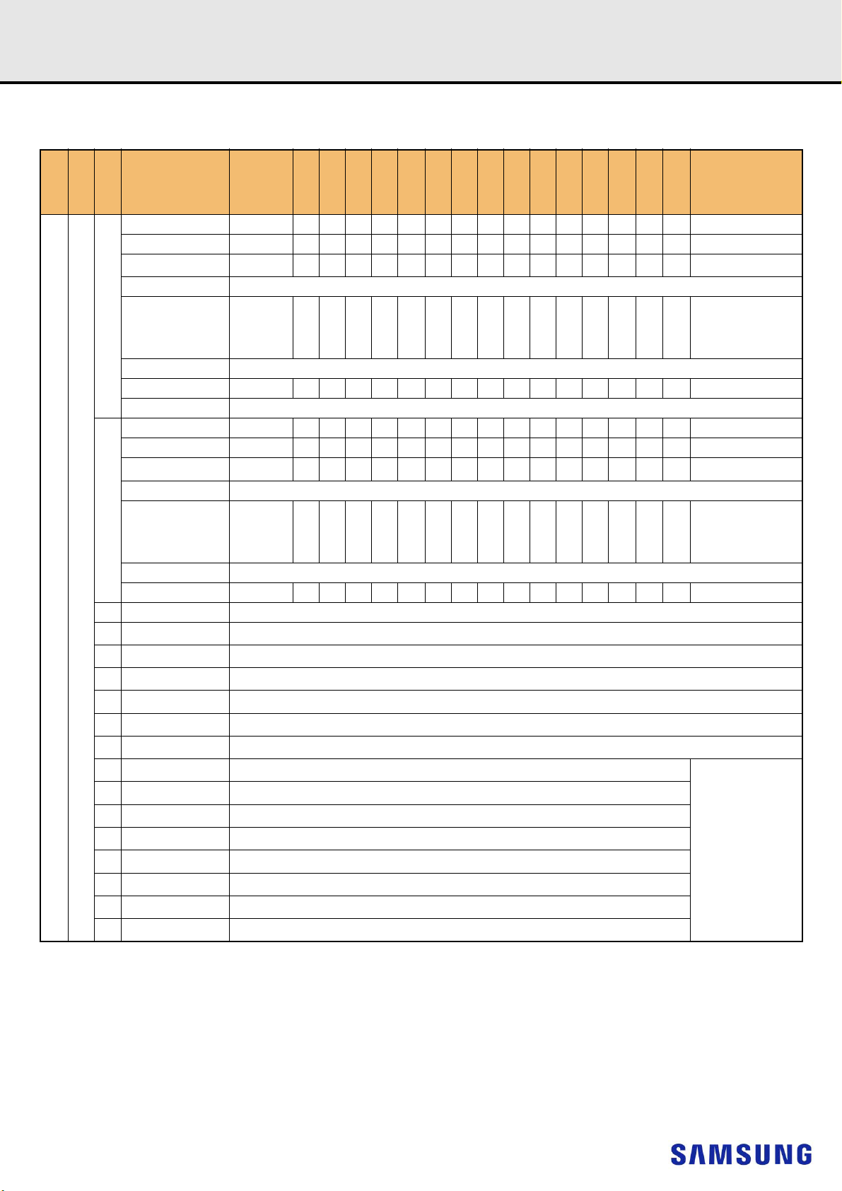
Rev. 1.3
Registered DIMM
[Table 43] IDD1, IDD1A and IPP1 Measurement-Loop Pattern
CKE
CK_t, CK_c
toggling
NOTE :
1) DQS_t, DQS_c are used according to RD Commands, otherwise VDDQ.
2) BG1 is don’t care for x16 device.
3) C[2:0] are used only for 3DS device.
4) Burst Sequence driven on each DQ signal by Read Command. Outside burst operation, DQ signals are VDDQ.
Sub-Loop
0
1
1*nRC + nRCD - AL RD 0110100110000 00
Static High
22*nRC
33*nRC
44*nRC
55*nRC
66*nRC
87*nRC
99*nRC
10 10*nRC
11 11*nR C
12 12*nRC
13 13*nRC
14 14*nRC
15 15*nRC
16 16*nRC
Cycle
Number
0 ACT 000000000000000 -
1, 2 D, D 100000000000000 -
3, 4 D#, D# 1111100
... repeat pattern 1...4 until nRCD - AL - 1, truncate if necessary
nRCD -AL RD 01101 0000000 0 0 0
... repeat pattern 1...4 until nRAS - 1, truncate if necessary
nRAS PRE 010100000000000 -
... repeat pattern 1...4 until nRC - 1, truncate if necessary
1*nRC + 0 ACT 000110011000000 -
1*nRC + 1, 2 D, D 1000 0 0000000000 -
1*nRC + 3, 4 D#, D# 11111 00
... repeat pattern nRC + 1...4 until 1*nRC + nRAS - 1, truncate if necessary
... repeat pattern 1...4 until nRAS - 1, truncate if necessary
1*nRC + nRAS PRE 010100110000000 -
... repeat nRC + 1...4 until 2*nRC - 1, truncate if necessary
Command
repeat Sub-Loop 0, use BG[1:0]
repeat Sub-Loop 1, use BG[1:0]
repeat Sub-Loop 0, use BG[1:0]
repeat Sub-Loop 1, use BG[1:0]
repeat Sub-Loop 0, use BG[1:0]
repeat Sub-Loop 1, use BG[1:0]
repeat Sub-Loop 1, use BG[1:0]
repeat Sub-Loop 0, use BG[1:0]
repeat Sub-Loop 1, use BG[1:0]
repeat Sub-Loop 0, use BG[1:0]
repeat Sub-Loop 1, use BG[1:0]
repeat Sub-Loop 0, use BG[1:0]
repeat Sub-Loop 1, use BG[1:0]
repeat Sub-Loop 0, use BG[1:0]
datasheet
1)
3)
CS_n
ACT_n
RAS_n/A16
CAS_n/A15
2)
2)
2)
2)
2)
2)
2)
2)
2)
2)
2)
2)
2)
2)
ODT
WE_n/A14
= 0, BA[1:0] = 2 instead
= 1, BA[1:0] = 3 instead
= 0, BA[1:0] = 1 instead
= 1, BA[1:0] = 2 instead
= 0, BA[1:0] = 3 instead
= 1, BA[1:0] = 0 instead
= 2, BA[1:0] = 0 instead
= 3, BA[1:0] = 1 instead
= 2, BA[1:0] = 2 instead
= 3, BA[1:0] = 3 instead
= 2, BA[1:0] = 1 instead
= 3, BA[1:0] = 2 instead
= 2, BA[1:0] = 3 instead
= 3, BA[1:0] = 0 instead
2)
C[2:0]
BA[1:0]
BG[1:0]
b)
30007 F0 -
3
b)
30007 F0 -
3
A12/BC_n
A[17,13,11]
DDR4 SDRAM
A[9:7]
A[6:3]
A[10]/AP
A[2:0]
D0=00, D1=FF
D2=FF, D3=00
D4=FF, D5=00
D6=00, D7=FF
D0=FF, D1=00
D2=00, D3=FF
D4=00, D5=FF
D6=FF, D7=00
For x4 and x8 only
Data
4)
- 56 -
Page 65

Rev. 1.3
Registered DIMM
datasheet
DDR4 SDRAM
[Table 44] IDD2N, IDD2NA, IDD2NL, IDD2NG, IDD2ND, IDD2N_par, IPP2,IDD3N, IDD3NA and IDD3P Measurement-Loop Pattern
2)
3)
CK_t, CK_c
CKE
Sub-Loop
Cycle
Number
Command
CS_n
ACT_n
RAS_n/A16
CAS_n/A15
WE_n/A14
ODT
A[9:7]
A[6:3]
C[2:0]
BA[1:0]
BG[1:0]
A12/BC_n
A[10]/AP
A[17,13,11]
A[2:0]
0 D, D 1000000000000000
1 D, D 1000000000000000
0
2 D#, D# 1 1 1 1 1 0 0
3 D#, D# 1 1 1 1 1 0 0
14-7
28-11
3 12-15
4 16-19
5 20-23
6 24-27
toggling
Static High
7 28-31
8 32-35
9 36-39
10 40-43
11 44-47
12 48-51
13 52-55
14 56-59
15 60-63
NOTE :
1) DQS_t, DQS_c are VDDQ.
2) BG1 is don’t care for x16 device.
3) C[2:0] are used only for 3DS device.
4) DQ signals are VDDQ.
repeat Sub-Loop 0, use BG[1:0]
repeat Sub-Loop 0, use BG[1:0]
repeat Sub-Loop 0, use BG[1:0]
repeat Sub-Loop 0, use BG[1:0]
repeat Sub-Loop 0, use BG[1:0]
repeat Sub-Loop 0, use BG[1:0]
repeat Sub-Loop 0, use BG[1:0]
repeat Sub-Loop 0, use BG[1:0]
repeat Sub-Loop 0, use BG[1:0]
repeat Sub-Loop 0, use BG[1:0]
repeat Sub-Loop 0, use BG[1:0]
repeat Sub-Loop 0, use BG[1:0]
repeat Sub-Loop 0, use BG[1:0]
repeat Sub-Loop 0, use BG[1:0]
repeat Sub-Loop 0, use BG[1:0]
2)
= 1, BA[1:0] = 1 instead
2)
= 0, BA[1:0] = 2 instead
2)
= 1, BA[1:0] = 3 instead
2
) = 0, BA[1:0] = 1 instead
2)
= 1, BA[1:0] = 2 instead
2)
= 0, BA[1:0] = 3 instead
2)
= 1, BA[1:0] = 0 instead
2)
= 2, BA[1:0] = 0 instead
2)
= 3, BA[1:0] = 1 instead
2)
= 2, BA[1:0] = 2 instead
2)
= 3, BA[1:0] = 3 instead
2)
= 2, BA[1:0] = 1 instead
2)
= 3, BA[1:0] = 2 instead
2)
= 2, BA[1:0] = 3 instead
2)
= 3, BA[1:0] = 0 instead
2)
3 000 7F00
3
2)
3 000 7F00
3
1)
4)
Data
- 57 -
Page 66
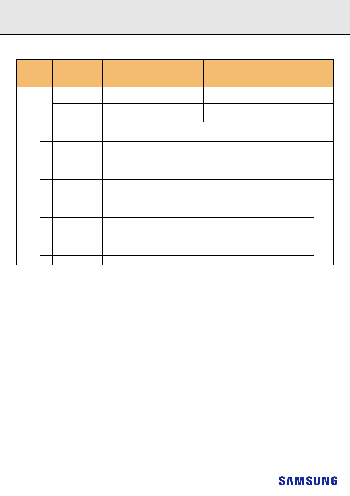
Rev. 1.3
Registered DIMM
datasheet
[Table 45] IDD2NT and IDDQ2NT Measurement-Loop Pattern
CK_t, CK_c
CKE
Sub-Loop
Cycle
Number
Command
CS_n
0D, D100000000000000-
1D, D100000000000000-
0
2 D#, D# 1111 100
3 D#, D# 1111 100
14-7
28-11
3 12-15
4 16-19
5 20-23
6 24-27
toggling
7 28-31
Static High
8 32-35
9 36-39
10 40-43
11 44-47
12 48-51
13 52-55
14 56-59
15 60-63
NOTE :
1) DQS_t, DQS_c are VDDQ.
2) BG1 is don’t care for x16 device.
3) C[2:0] are used only for 3DS device.
4) DQ signals are VDDQ.
repeat Sub-Loop 0, but ODT = 1 and BG[1:0]
repeat Sub-Loop 0, but ODT = 0 and BG[1:0]
repeat Sub-Loop 0, but ODT = 1 and BG[1:0]
repeat Sub-Loop 0, but ODT = 0 and BG[1:0]
repeat Sub-Loop 0, but ODT = 1 and BG[1:0]
repeat Sub-Loop 0, but ODT = 0 and BG[1:0]
repeat Sub-Loop 0, but ODT = 1 and BG[1:0]
repeat Sub-Loop 0, but ODT = 0 and BG[1:0]
repeat Sub-Loop 0, but ODT = 1 and BG[1:0]
repeat Sub-Loop 0, but ODT = 0 and BG[1:0]
repeat Sub-Loop 0, but ODT = 1 and BG[1:0]
repeat Sub-Loop 0, but ODT = 0 and BG[1:0]
repeat Sub-Loop 0, but ODT = 1 and BG[1:0]
repeat Sub-Loop 0, but ODT = 0 and BG[1:0]
repeat Sub-Loop 0, but ODT = 1 and BG[1:0]
DDR4 SDRAM
1)
2)
3)
ACT_n
RAS_n/A16
CAS_n/A15
WE_n/A14
ODT
C[2:0]
2)
= 1, BA[1:0] = 1 instead
2)
= 0, BA[1:0] = 2 instead
2)
= 1, BA[1:0] = 3 instead
2)
= 0, BA[1:0] = 1 instead
2)
= 1, BA[1:0] = 2 instead
2)
= 0, BA[1:0] = 3 instead
2)
= 1, BA[1:0] = 0 instead
2)
= 2, BA[1:0] = 0 instead
2)
= 3, BA[1:0] = 1 instead
2)
= 2, BA[1:0] = 2 instead
2)
= 3, BA[1:0] = 3 instead
2)
= 2, BA[1:0] = 1 instead
2)
= 3, BA[1:0] = 2 instead
2)
= 2, BA[1:0] = 3 instead
2)
= 3, BA[1:0] = 0 instead
BA[1:0]
BG[1:0]
2
3 0007F0-
3
2
3 0007F0-
3
A12/BC_n
A[17,13,11]
A[9:7]
A[6:3]
A[10]/AP
A[2:0]
4)
Data
For x4
and x8
only
- 58 -
Page 67

Rev. 1.3
Registered DIMM
[Table 46] IDD4R, IDDR4RA, IDD4RB and IDDQ4R Measurement-Loop Pattern
CKE
CK_t, CK_c
toggling
Static High
NOTE :
1) DQS_t, DQS_c are used according to RD Commands, otherwise VDDQ.
2) BG1 is don’t care for x16 device.
3) C[2:0] are used only for 3DS device.
4) Burst Sequence driven on each DQ signal by Read Command.
Cycle
Sub-Loop
0
1
28-11
3 12-15
4 16-19
5 20-23
6 24-27
7 28-31
8 32-35
9 36-39
10 40-43
11 44-47
12 48-51
13 52-55
14 56-59
15 60-63
Number
0 RD 011010000000000
1 D 100000000000 000-
2,3 D#, D# 1 1 1 1 1 0 0
4 RD 0110100110007F0
5 D 100000000000 000-
6,7 D#, D# 1 1 1 1 1 0 0
Command
repeat Sub-Loop 0, use BG[1:0]
repeat Sub-Loop 1, use BG[1:0]
repeat Sub-Loop 0, use BG[1:0]
repeat Sub-Loop 1, use BG[1:0]
repeat Sub-Loop 0, use BG[1:0]
repeat Sub-Loop 1, use BG[1:0]
repeat Sub-Loop 0, use BG[1:0]
repeat Sub-Loop 1, use BG[1:0]
repeat Sub-Loop 0, use BG[1:0]
repeat Sub-Loop 1, use BG[1:0]
repeat Sub-Loop 0, use BG[1:0]
repeat Sub-Loop 1, use BG[1:0]
repeat Sub-Loop 0, use BG[1:0]
repeat Sub-Loop 1, use BG[1:0]
CS_n
datasheet
3)
ACT_n
RAS_n/A16
CAS_n/A15
2)
2)
2)
2)
2)
2)
2)
2)
2)
2)
2)
2)
2)
2)
ODT
WE_n/A14
= 0, BA[1:0] = 2 instead
= 1, BA[1:0] = 3 instead
= 0, BA[1:0] = 1 instead
= 1, BA[1:0] = 2 instead
= 0, BA[1:0] = 3 instead
= 1, BA[1:0] = 0 instead
= 2, BA[1:0] = 0 instead
= 3, BA[1:0] = 1 instead
= 2, BA[1:0] = 2 instead
= 3, BA[1:0] = 3 instead
= 2, BA[1:0] = 1 instead
= 3, BA[1:0] = 2 instead
= 2, BA[1:0] = 3 instead
= 3, BA[1:0] = 0 instead
C[2:0]
3
3
DDR4 SDRAM
1)
2)
4)
A[9:7]
A[6:3]
BA[1:0]
BG[1:0]
2)
2)
A12/BC_n
3 000 7F0-
3 000 7F0-
A[10]/AP
A[17,13,11]
A[2:0]
Data
D0=00, D1=FF
D2=FF, D3=00
D4=FF, D5=00
D6=00, D7=FF
D0=FF, D1=00
D2=00, D3=FF
D4=00, D5=FF
D6=FF, D7=00
For x4 and x8 only
- 59 -
Page 68
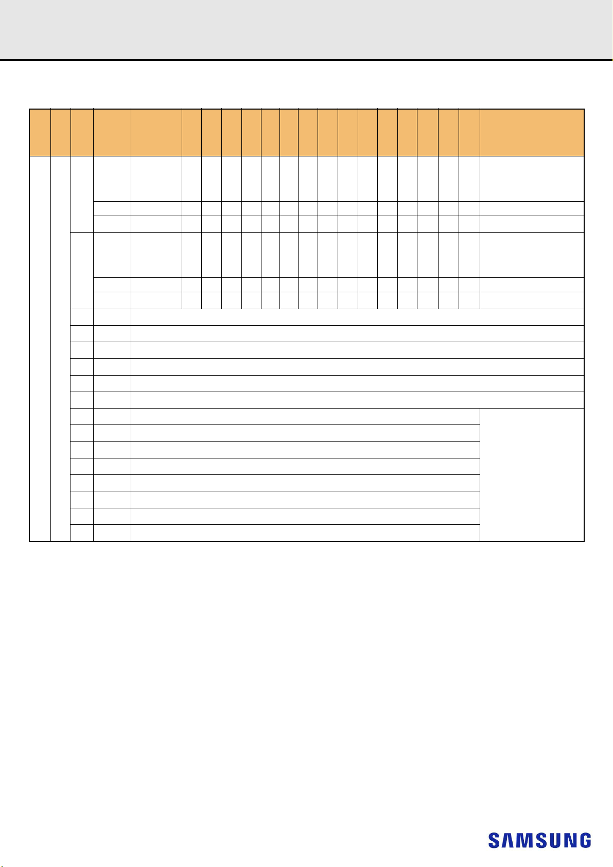
Rev. 1.3
Registered DIMM
[Table 47] IDD4W, IDD4WA, IDD4WB and IDD4W_par Measurement-Loop Pattern
CKE
CK_t, CK_c
toggling
Static High
NOTE :
1) DQS_t, DQS_c are used according to WR Commands, otherwise VDDQ.
2) BG1 is don’t care for x16 device.
3) C[2:0] are used only for 3DS device.
4) Burst Sequence driven on each DQ signal by Write Command.
Cycle
Sub-Loop
0
1
28-11
3 12-15
4 16-19
5 20-23
6 24-27
7 28-31
8 32-35
9 36-39
10 40-43
11 44-47
12 48-51
13 52-55
14 56-59
15 60-63
Number
0 WR 011001000000000
1 D 100001000000000-
2,3 D#, D# 1111110
4 WR 0110010110007F0
5 D 100001000000000-
6,7 D#, D# 1111110
Command
repeat Sub-Loop 0, use BG[1:0]
repeat Sub-Loop 1, use BG[1:0]
repeat Sub-Loop 0, use BG[1:0]
repeat Sub-Loop 1, use BG[1:0]
repeat Sub-Loop 0, use BG[1:0]
repeat Sub-Loop 1, use BG[1:0]
repeat Sub-Loop 0, use BG[1:0]
repeat Sub-Loop 1, use BG[1:0]
repeat Sub-Loop 0, use BG[1:0]
repeat Sub-Loop 1, use BG[1:0]
repeat Sub-Loop 0, use BG[1:0]
repeat Sub-Loop 1, use BG[1:0]
repeat Sub-Loop 0, use BG[1:0]
repeat Sub-Loop 1, use BG[1:0]
CS_n
datasheet
3)
ACT_n
RAS_n/A16
CAS_n/A15
2)
2)
2)
2)
2)
2)
2)
2)
2)
2)
2)
2)
2)
2)
ODT
WE_n/A14
= 0, BA[1:0] = 2 instead
= 1, BA[1:0] = 3 instead
= 0, BA[1:0] = 1 instead
= 1, BA[1:0] = 2 instead
= 0, BA[1:0] = 3 instead
= 1, BA[1:0] = 0 instead
= 2, BA[1:0] = 0 instead
= 3, BA[1:0] = 1 instead
= 2, BA[1:0] = 2 instead
= 3, BA[1:0] = 3 instead
= 2, BA[1:0] = 1 instead
= 3, BA[1:0] = 2 instead
= 2, BA[1:0] = 3 instead
= 3, BA[1:0] = 0 instead
C[2:0]
2)
BG[1:0]
2)
3
2)
3
DDR4 SDRAM
1)
4)
A[9:7]
A[6:3]
BA[1:0]
A12/BC_n
3 0007F0-
3 0007F0-
A[10]/AP
A[17,13,11]
A[2:0]
Data
D0=00, D1=FF
D2=FF, D3=00
D4=FF, D5=00
D6=00, D7=FF
D0=FF, D1=00
D2=00, D3=FF
D4=00, D5=FF
D6=FF, D7=00
For x4 and x8 only
- 60 -
Page 69
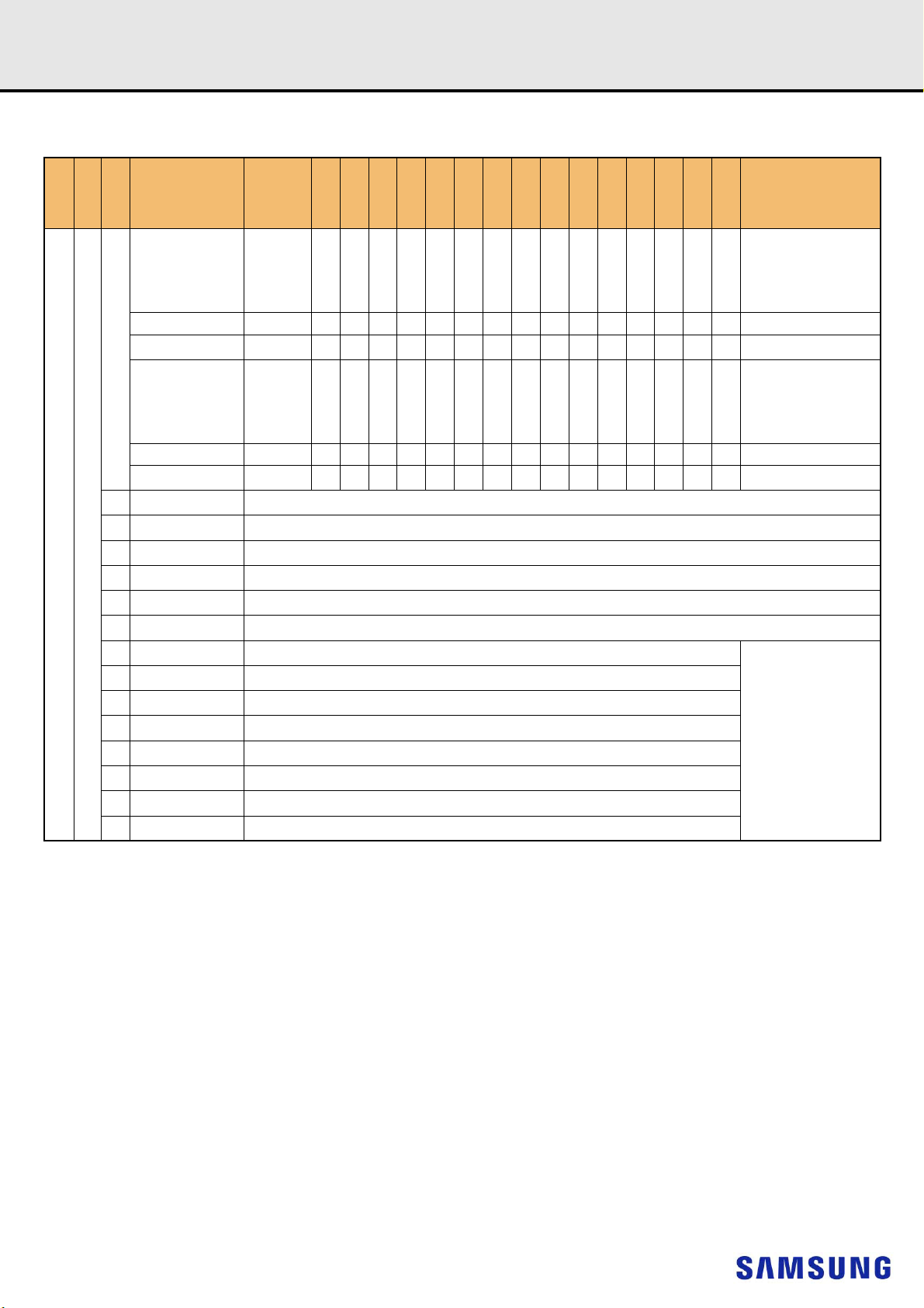
Rev. 1.3
Registered DIMM
[Table 48] IDD4WC Measurement-Loop Pattern
CKE
CK_t, CK_c
toggling
NOTE :
1) DQS_t, DQS_c are VDDQ.
2) BG1 is don’t care for x16 device.
3) C[2:0] are used only for 3DS device.
4) Burst Sequence driven on each DQ signal by Write Command.
Sub-Loop
0
2 10-14
3 15-19
4 20-24
Static High
5 25-29
6 30-34
7 35-39
8 40-44
9 45-49
10 50-54
11 5 5-5 9
12 60-64
13 65-69
14 70-74
15 75-79
Cycle
Number
0 WR 011001000000000
1,2 D, D 100001000000000-
3,4 D#, D# 1111110
5 WR 0110010110007F0
6,7 D, D 100001000000000-
8,9 D#, D# 1111110
repeat Sub-Loop 0, use BG[1:0]
repeat Sub-Loop 1, use BG[1:0]
repeat Sub-Loop 0, use BG[1:0]
repeat Sub-Loop 1, use BG[1:0]
repeat Sub-Loop 0, use BG[1:0]
repeat Sub-Loop 1, use BG[1:0]
repeat Sub-Loop 0, use BG[1:0]
repeat Sub-Loop 1, use BG[1:0]
repeat Sub-Loop 0, use BG[1:0]
repeat Sub-Loop 1, use BG[1:0]
repeat Sub-Loop 0, use BG[1:0]
repeat Sub-Loop 1, use BG[1:0]
repeat Sub-Loop 0, use BG[1:0]
repeat Sub-Loop 1, use BG[1:0]
1)
CS_n
Command
datasheet
2)
3)
ACT_n
RAS_n/A16
CAS_n/A15
ODT
C[2:0]
WE_n/A14
2)
= 0, BA[1:0] = 2 instead
2)
= 1, BA[1:0] = 3 instead
2)
= 0, BA[1:0] = 1 instead
2)
= 1, BA[1:0] = 2 instead
2)
= 0, BA[1:0] = 3 instead
2)
= 1, BA[1:0] = 0 instead
2)
= 2, BA[1:0] = 0 instead
2)
= 3, BA[1:0] = 1 instead
2)
= 2, BA[1:0] = 2 instead
2)
= 3, BA[1:0] = 3 instead
2)
= 2, BA[1:0] = 1 instead
2)
= 3, BA[1:0] = 2 instead
2)
= 2, BA[1:0] = 3 instead
2)
= 3, BA[1:0] = 0 instead
BG[1:0]
2)
3
2)
3
DDR4 SDRAM
4)
A[9:7]
A[6:3]
BA[1:0]
A12/BC_n
3 0007F0-
3 0007F0-
A[10]/AP
A[17,13,11]
A[2:0]
Data
D0=00, D1=FF
D2=FF, D3=00
D4=FF, D5=00
D6=00, D7=FF
D8=CRC
D0=FF, D1=00
D2=00, D3=FF
D4=00, D5=FF
D6=FF, D7=00
D8=CRC
For x4 and x8 only
- 61 -
Page 70
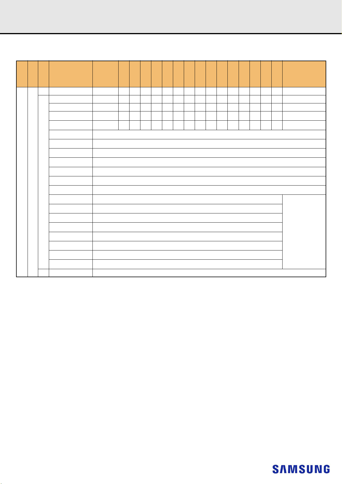
Rev. 1.3
Registered DIMM
[Table 49] IDD5B Measurement-Loop Pattern
CKE
CK_t, CK_c
Sub-Loop
00 REF 100000000000000-
1
toggling
Static High
2 64 ... nRFC - 1 repeat Sub-Loop 1, Truncate, if necessary
NOTE :
1) DQS_t, DQS_c are VDDQ.
2) BG1 is don’t care for x16 device.
3) C[2:0] are used only for 3DS device.
4) DQ signals are VDDQ.
Cycle
Number
Command
1 D 100000000000000-
2 D 100000000000000-
3 D#, D# 1111100
4 D#, D# 1111100
4-7
8-11
12-15
16-19
20-23
24-27
28-31
32-35
36-39
40-43
44-47
48-51
52-55
56-59
60-63
repeat pattern 1...4, use BG[1:0]
repeat pattern 1...4, use BG[1:0]
repeat pattern 1...4, use BG[1:0]
repeat pattern 1...4, use BG[1:0]
repeat pattern 1...4, use BG[1:0]
repeat pattern 1...4, use BG[1:0]
repeat pattern 1...4, use BG[1:0]
repeat pattern 1...4, use BG[1:0]
repeat pattern 1...4, use BG[1:0]
repeat pattern 1...4, use BG[1:0]
repeat pattern 1...4, use BG[1:0]
repeat pattern 1...4, use BG[1:0]
repeat pattern 1...4, use BG[1:0]
repeat pattern 1...4, use BG[1:0]
repeat pattern 1...4, use BG[1:0]
datasheet
1)
2)
3)
CS_n
ACT_n
RAS_n/A16
CAS_n/A15
ODT
C[2:0]
WE_n/A14
2)
= 1, BA[1:0] = 1 instead
2)
= 0, BA[1:0] = 2 instead
2)
= 1, BA[1:0] = 3 instead
2)
= 0, BA[1:0] = 1 instead
2)
= 1, BA[1:0] = 2 instead
2)
= 0, BA[1:0] = 3 instead
2)
= 1, BA[1:0] = 0 instead
2)
= 2, BA[1:0] = 0 instead
2)
= 3, BA[1:0] = 1 instead
2)
= 2, BA[1:0] = 2 instead
2)
= 3, BA[1:0] = 3 instead
2)
= 2, BA[1:0] = 1 instead
2)
= 3, BA[1:0] = 2 instead
2)
= 2, BA[1:0] = 3 instead
2)
= 3, BA[1:0] = 0 instead
BG[1:0]
2)
3
2)
3
BA[1:0]
A12/BC_n
A[17,13,11]
3 0007F0-
3 0007F0-
DDR4 SDRAM
A[9:7]
A[6:3]
A[10]/AP
A[2:0]
For x4 and x8 only
Data
4)
- 62 -
Page 71
Rev. 1.3
Registered DIMM
[Table 50] IDD7 Measurement-Loop Pattern
CK_t, CK_c
CKE
Sub-Loop
0 ACT 000000000000000 -
1 RDA 011010 00001000
0
2 D 100000000000000-
3 D# 1111100
... repeat pattern 2...3 until nRRD - 1, if nRRD > 4. Truncate if necessary
nRRD ACT 000000011000000 -
1
nRRD + 1 RDA 011010 11001000
... repeat pattern 2 ... 3 until 2*nRRD - 1, if nRRD > 4. Truncate if necessary
2 2*nRRD
3 3*nRRD
4 4*nRRD repeat pattern 2 ... 3 until nFAW - 1, if nFAW > 4*nRRD. Truncate if necessary
Cycle
Number
repeat Sub-Loop 0, use BG[1:0]
repeat Sub-Loop 1, use BG[1:0]
1)
Command
datasheet
3)
CS_n
ACT_n
RAS_n/A16
CAS_n/A15
2)
2)
ODT
WE_n/A14
= 0, BA[1:0] = 2 instead
= 1, BA[1:0] = 3 instead
C[2:0]
DDR4 SDRAM
2)
A[9:7]
BA[1:0]
BG[1:0]
2
3
A12/BC_n
3 0007F0-
A[10]/AP
A[17,13,11]
A[6:3]
Data
A[2:0]
D0=00, D1=FF
D2=FF, D3=00
D4=FF, D5=00
D6=00, D7=FF
D0=FF, D1=00
D2=00, D3=FF
D4=00, D5=FF
D6=FF, D7=00
4)
5nFAW
6 nFAW + nRRD
toggling
NOTE:
1) DQS_t, DQS_c are VDDQ.
2) BG1 is don’t care for x16 device.
3) C[2:0] are used only for 3DS device.
4) Burst Sequence driven on each DQ signal by Read Command. Outside burst operation, DQ signals are VDDQ.
7 nFAW + 2*nRRD
Static High
8 nFAW + 3*nRRD
9 nFAW + 4*nRRD repeat Sub-Loop 4
10 2*nFAW
11 2*nFAW + nRRD
12 2*nFAW + 2*nRRD
13 2*nFAW + 3*nRRD
14 2*nFAW + 4*nRRD repeat Sub-Loop 4
15 3*nFAW
16 3*nFAW + nRRD
17 3*nFAW + 2*nRRD
18 3*nFAW + 3*nRRD
19 3*nFAW + 4*nRRD repeat Sub-Loop 4
20 4*nFAW repeat pattern 2 ... 3 until nRC - 1, if nRC > 4*nFAW. Truncate if necessary
repeat Sub-Loop 0, use BG[1:0]
repeat Sub-Loop 1, use BG[1:0]
repeat Sub-Loop 0, use BG[1:0]
repeat Sub-Loop 1, use BG[1:0]
repeat Sub-Loop 0, use BG[1:0]
repeat Sub-Loop 1, use BG[1:0]
repeat Sub-Loop 0, use BG[1:0]
repeat Sub-Loop 1, use BG[1:0]
repeat Sub-Loop 0, use BG[1:0]
repeat Sub-Loop 1, use BG[1:0]
repeat Sub-Loop 0, use BG[1:0]
repeat Sub-Loop 1, use BG[1:0]
2)
= 0, BA[1:0] = 1 instead
2)
= 1, BA[1:0] = 2 instead
2)
= 0, BA[1:0] = 3 instead
2)
= 1, BA[1:0] = 0 instead
2)
= 2, BA[1:0] = 0 instead
2)
= 3, BA[1:0] = 1 instead
2)
= 2, BA[1:0] = 2 instead
2)
= 3, BA[1:0] = 3 instead
2)
= 2, BA[1:0] = 1 instead
2)
= 3, BA[1:0] = 2 instead
2)
= 2, BA[1:0] = 3 instead
2)
= 3, BA[1:0] = 0 instead
For x4 and x8 only
- 63 -
Page 72
Rev. 1.3
Registered DIMM
datasheet
DDR4 SDRAM
19. TIMING PARAMETERS BY SPEED GRADE
[Table 51] Timing Parameters by Speed Bin for DDR4-1600 to DDR4-2933
Speed DDR4-1600 DDR4-1866 DDR4-2133 DDR4-2400 DDR4-2666 DDR4-2933
Parameter Symbol MIN MAX MIN MAX MIN MAX MIN MAX MIN MAX MIN MAX
Clock Timing
Minimum Clock Cycle Time
(DLL off mode)
Average Clock Period tCK(avg) 1.25 <1.5 1.071 <1.25 0.937 <1.071 0.833 <0.937 0.750 <0.833 0.682 <0.750 ns 35,36
Average high pulse width tCH(avg) 0.48 0.52 0.48 0.52 0.48 0.52 0.48 0.52 0.48 0.52 0.48 0.52 tCK(avg)
Average low pulse width tCL(avg) 0.48 0.52 0.48 0.52 0.48 0.52 0.48 0.52 0.48 0.52 0.48 0.52 tCK(avg)
Absolute Clock Period tCK(abs)
Absolute clock HIGH pulse width tCH(abs) 0.45 - 0.45 - 0.45 - 0.45 - 0.45 - 0.45 - tCK(avg) 23
Absolute clock LOW pulse width tCL(abs) 0.45 - 0.45 - 0.45 - 0.45 - 0.45 - 0.45 - tCK(avg) 24
Clock Period Jitter- total JIT(per)_tot -63 63 -54 54 -47 47 -42 42 -38 38 -34 34 ps 23
Clock Period Jitter- deterministic JIT(per)_dj -31 31 -27 27 -23 23 -21 21 -19 19 -17 17 ps 26
Clock Period Jitter during DLL locking
period
Cycle to Cycle Period Jitter tJIT(cc) - 125 - 107 - 94 - 83 - 75 - 68 ps
Cycle to Cycle Period Jitter during DLL
locking period
Duty Cycle Jitter tJIT(duty) TBD TBD TBD TBD TBD TBD TBD TBD TBD TBD TBD TBD ps
Cumulative error across 2 cycles tERR(2per) -92 92 -79 79 -69 69 -61 61 -55 55 -50 50 ps
Cumulative error across 3 cycles tERR(3per) -109 109 -94 94 -82 82 -73 73 -66 66 -60 60 ps
Cumulative error across 4 cycles tERR(4per) -121 121 -104 104 -91 91 -81 81 -73 73 -66 66 ps
Cumulative error across 5 cycles tERR(5per) -131 131 -112 112 -98 98 -87 87 -78 78 -71 71 ps
Cumulative error across 6 cycles tERR(6per) -139 139 -119 119 -104 104 -92 92 -83 83 -75 75 ps
Cumulative error across 7 cycles tERR(7per) -145 145 -124 124 -109 109 -97 97 -87 87 -79 79 ps
Cumulative error across 8 cycles tERR(8per) -151 151 -129 129 -113 113 -101 101 -91 91 -83 83 ps
Cumulative error across 9 cycles tERR(9per) -156 156 -134 134 -117 117 -104 104 -94 94 -85 85 ps
Cumulative error across 10 cycles tERR(10per) -160 160 -137 137 -120 120 -107 107 -96 96 -88 88 ps
Cumulative error across 11 cycles tERR(11per) -164 164 -141 141 -123 123 -110 110 -99 99 -90 90 ps
Cumulative error across 12 cycles tERR(12per) -168 168 -144 144 -126 126 -112 112 -101 101 -92 92 ps
Cumulative error across 13 cycles tERR(13per) -172 172 -147 147 -129 129 -114 114 -103 103 -93 93 ps
Cumulative error across 14 cycles tERR(14per) -175 175 -150 150 -131 131 -116 116 -104 104 -95 95 ps
Cumulative error across 15 cycles tERR(15per) -178 178 -152 152 -133 133 -118 118 -106 106 -97 97 ps
Cumulative error across 16 cycles tERR(16per) -180 189 -155 155 -135 135 -120 120 -108 108 -98 98 ps
Cumulative error across 17 cycles tERR(17per) -183 183 -157 157 -137 137 -122 122 -110 110 -100 100 ps
Cumulative error across 18 cycles tERR(18per) -185 185 -159 159 -139 139 -124 124 -112 112 -101 101 ps
Cumulative error across n = 13, 14 . . .
49, 50 cycles
Command and Address setup time to
CK_t, CK_c referenced to Vih(ac) /
Vil(ac) levels
Command and Address setup time to
CK_t, CK_c referenced to Vref levels
Command and Address hold time to
CK_t, CK_c referenced to Vih(dc) /
Vil(dc) levels
Command and Address hold time to
CK_t, CK_c referenced to Vref levels
Control and Address Input pulse width
for each input
Command and Address Timing
CAS_n to CAS_n command delay for
same bank group
CAS_n to CAS_n command delay for
different bank group
ACTIVATE to ACTIVATE Command
delay to different bank group for 2KB
page size
ACTIVATE to ACTIVATE Command
delay to different bank group for 2KB
page size
ACTIVATE to ACTIVATE Command
delay to different bank group for 1/2KB
page size
tCK
(DLL_OFF)
tJIT(per, lck) -50 50 -43 43 -38 38 -33 33 -30 30 -27 27 ps
tJIT(cc, lck) - 100 - 86 - 75 - 67 - 60 - 55 ps
tERR(nper)
tIS(base) 115 - 100 - 80 - 62 - 55 - 48 - ps
tIS(Vref) 215 - 200 - 180 - 162 - 145 - 138 - ps
tIH(base) 140 - 125 - 105 - 87 - 80 - 73 - ps
tIH(Vref) 215 - 200 - 180 - 162 - 145 - 138 - ps
tIPW 600 - 525 - 460 - 410 - 385 - 365 - ps
tCCD_L
tCCD_S 4 - 4 - 4 - 4 - 4 - 4 - nCK 34
tRRD_S(2K)
tRRD_S(1K)
tRRD_S(1/2K)
820820820820820820ns
MIN : tCK(avg)min + tJIT(per)min_tot
MAX : tCK(avg)max + tJIT(per)max_tot
max(5
nCK,
6.250 ns)
Max(4nCK
,6ns)
Max(4nCK
,5ns)
Max(4nCK
,5ns)
-
-
max(5
nCK,
5.355 ns)
Max(4nCK
,5.3ns)
Max(4nCK
,4.2ns)
Max(4nCK
,4.2ns)
MIN : tERR(nper)min = ((1 + 0.68ln(n)) * tJIT(per)_total min)
MAX : tERR(nper)max = ((1 + 0.68ln(n)) *
max(5
-
-
nCK,
5.355 ns)
Max(4nCK
,5.3ns)
Max(4nCK
,3.7ns)
Max(4nCK
,3.7ns)
-
-
max(5
nCK,
5 ns)
Max(4nCK
,5.3ns)
Max(4nCK
,3.3ns)
Max(4nCK
,3.3ns)
t
JIT(per)_total max)
-
Max(4nCK
-
Max(4nCK
-
Max(4nCK
-
max(5
nCK,
5 ns)
,5.3ns)
,3ns)
,3ns)
-
-
-
-
max(5
nCK,
5 ns)
Max(4nCK
,5.3ns)
Max(4nCK
,2.7ns)
Max(4nCK
,2.7ns)
Units NOTE
tCK(avg)
ps
-nCK34
-nCK34
-nCK34
-nCK34
- 64 -
Page 73

Rev. 1.3
Registered DIMM
datasheet
DDR4 SDRAM
[Table 51] Timing Parameters by Speed Bin for DDR4-1600 to DDR4-2933
Speed DDR4-1600 DDR4-1866 DDR4-2133 DDR4-2400 DDR4-2666 DDR4-2933
Parameter Symbol MIN MAX MIN MAX MIN MAX MIN MAX MIN MAX MIN MAX
ACTIVATE to ACTIVATE Command
delay to same bank group for 2KB
page size
ACTIVATE to ACTIVATE Command
delay to same bank group for 1KB
page size
ACTIVATE to ACTIVATE Command
delay to same bank group for 1/2KB
page size
Four activate window for 2KB page
size
Four activate window for 1KB page
size
Four activate window for 1/2KB page
size
Delay from start of internal write transaction to internal read command for different bank group
Delay from start of internal write transaction to internal read command for
same bank group
Internal READ Command to PRECHARGE Command delay
WRITE recovery time tWR 15 - 15 - 15 - 15 - 15 - 15 - ns 1
Write recovery time when CRC and DM
are enabled
Delay from start of internal write transaction to internal read command for different bank group with both CRC and
DM enabled
Delay from start of internal write transaction to internal read command for
same bank group with both CRC and
DM enabled
DLL locking time tDLLK 597 - 597 - 768 - 768 - 854 - 940 - nCK
Mode Register Set command cycle
time
Mode Register Set command update
delay
Multi-Purpose Register Recovery Time tMPRR 1 - 1 - 1 - 1 - 1 - 1 - nCK 33
Multi Purpose Register Write Recovery
Time
Auto precharge write recovery + precharge time
DQ0 or DQL0 driven to 0 set-up time to
first DQS rising edge
DQ0 or DQL0 driven to 0 hold time
from last DQS falling edge
CS_n to Command Address Latency
CS_n to Command Address Latency tCAL
Mode Register Set command cycle
time in CAL mode
Mode Register Set update delay in
CAL mode
DRAM Data Timing
DQS_t, DQS_c to DQ skew, per group,
per access
DQ output hold time per group, per access from DQS_t, DQS_c
Data Valid Window per device, per UI:
(tQH - tDQSQ) of each UI on a given
DRAM
Data Valid Window, per pin, per UI:
(tQH - tDQSQ) each UI on a pin of a
given DRAM
DQ low impedance time from CK_t,
CK_c
DQ high impedance time from CK_t,
CK_c
Data Strobe Timing
DQS_t, DQS_c differential READ Preamble (1 clock preamble)
tRRD_L(2K)
tRRD_L(1K)
tRRD_L(1/2K)
tFAW_2K
tFAW_1K
tFAW_1/2K
tWTR_S
tWTR_L
tWR_CRC
tWTR_S_C
tWTR_L_C
tWR_MPR
tDAL(min) Programmed WR + roundup (tRP / tCK(avg)) nCK
tPDA_H 0.5 - 0.5 - 0.5 - 0.5 - 0.5 - 0.5 - UI 46,47
tMRD_tCAL
tMOD_tCAL
tLZ(DQ) -450 225 -390 195 -360 180 -330 175 -310 170 -280 165 ps 39
tHZ(DQ) - 225 -195- 180 - 175 - 170 - 165 ps 39
Max(4nCK
,7.5ns)
Max(4nCK
,6ns)
Max(4nCK
,6ns)
Max(28nC
K,35ns)
Max(20nC
K,25ns)
Max(16nC
K,20ns)
max(2nCK
,2.5ns)
max(4nCK
,7.5ns)
max(4nCK
tRTP
_DM
RC_DM
RC_DM
tMRD8-8-8-8-8-8-nCK
tMOD
tPDA_S 0.5 - 0.5 - 0.5 - 0.5 - 0.5 - 0.5 - UI 45,47
tDQSQ - 0.16 - 0.16 - 0.16 - 0.17 - 0.18 - 0.19
tDVWd 0.63 - 0.63 - 0.64 - 0.64 - TBD - TBD - UI
tDVWp 0.66 - 0.66 - 0.69 - 0.72 - 0.72 - TBD - UI
tRPRE 0.9 NOTE44 0.9 NOTE44 0.9 NOTE44 0.9 NOTE 44 0.9 NOTE 44 0.9 NOTE 44 tCK 40
,7.5ns)
tWR+max
(4nCK,3.7
5ns)
tWTR_S+
max
(4nCK,3.7
5ns)
tWTR_L+
max
(4nCK,3.7
5ns)
max(24nC
K,15ns)
tMOD
(min)
+ AL + PL
max(3
nCK, 3.748
ns)
tMOD+
tCAL
tMOD+
tCAL
tQH 0.76 - 0.76 - 0.76 - 0.74 - 0.74 - 0.72 -
-
-
-
-
-
-
-
-
-
-
-
Max(4nCK
,6.4ns)
Max(4nCK
,5.3ns)
Max(4nCK
,5.3ns)
Max(28nC
K,30ns)
Max(20nC
K,23ns)
Max(16nC
K,17ns)
max(2nCK
,2.5ns)
max(4nCK
,7.5ns)
max(4nCK
,7.5ns)
tWR+max
(5nCK,3.7
5ns)
tWTR_S+
max
(5nCK,3.7
5ns)
tWTR_L+
max
(5nCK,3.7
5ns)
max(24nC
K,15ns)
tMOD
(min)
+ AL + PL
max(3
nCK, 3.748
ns)
tMOD+
tCAL
tMOD+
tCAL
-
-
-
-
-
-
-
-
-
-
-
Max(4nCK
,6.4ns)
Max(4nCK
,5.3ns)
Max(4nCK
,5.3ns)
Max(28nC
K,30ns)
Max(20nC
K,21ns)
Max(16nC
K,15ns)
max(2nCK
,2.5ns)
max(4nCK
,7.5ns)
max(4nCK
,7.5ns)
tWR+max
(5nCK,3.7
5ns)
tWTR_S+
max
(5nCK,3.7
5ns)
tWTR_L+
max
(5nCK,3.7
5ns)
max(24nC
K,15ns)
tMOD
(min)
+ AL + PL
max(3
nCK, 3.748
ns)
tMOD+
tCAL
tMOD+
tCAL
-
-
-
-
-
-
-
-
-
-
-
Max(4nCK
,6.4ns)
Max(4nCK
,4.9ns)
Max(4nCK
,4.9ns)
Max(28nC
K,30ns)
Max(20nC
K,21ns)
Max(16nC
K,13ns)
Max
(2nCK,
2.5ns)
max
(4nCK,7.5
ns)
max
(4nCK,7.5
ns)
tWR+max
(5nCK,3.7
5ns)
tWTR_S+
max
(5nCK,3.7
5ns)
tWTR_L+
max
(5nCK,3.7
5ns)
max(24nC
K,15ns)
tMOD
(min)
+ AL + PL
max(3
nCK, 3.748
ns)
tMOD+
tCAL
tMOD+
tCAL
-
-
-
-
-
-
-
-
-
-
-
-
-
-
-
-
-
Max(4nCK
,6.4ns)
Max(4nCK
,4.9ns)
Max(4nCK
,4.9ns)
Max(28nC
K,30ns)
Max(20nC
K,21ns)
Max(16nC
K,12ns)
Max
(2nCK,
2.5ns)
max
(4nCK,7.5
ns)
max
(4nCK,7.5
ns)
tWR+max
(5nCK,3.7
5ns)
tWTR_S+
max
(5nCK,3.7
5ns)
tWTR_L+
max
(5nCK,3.7
5ns)
max(24nC
K,15ns)
tMOD
(min)
+ AL + PL
max(3
nCK, 3.748
ns)
tMOD+
tCAL
tMOD+
tCAL
-
-
-
-
-
-
-
-
-
-
-
-
-
-
-
-
-
Max(4nCK
,6.4ns)
Max(4nCK
,4.9ns)
Max(4nCK
,4.9ns)
Max(28nC
K,30ns)
Max(20nC
K,21ns)
Max
(16nCK,
10.875ns)
Max
(2nCK,
2.5ns)
max
(4nCK,7.5
ns)
max
(4nCK,7.5
ns)
tWR+max
(5nCK,3.7
5ns)
tWTR_S+
max
(5nCK,3.7
5ns)
tWTR_L+
max
(5nCK,3.7
5ns)
max(24nC
K,15ns)
tMOD
(min)
+ AL + PL
max(3
nCK, 3.748
ns)
tMOD+
tCAL
tMOD+
tCAL
Units NOTE
-nCK34
-nCK34
-nCK34
-ns34
-ns34
-ns34
-ns
-1,34
-
-ns1, 28
-ns
- ns 3,30, 34
-nCK50
-
-nCK
-nCK
-nCK
tCK(avg)/213,18,3
tCK(avg)/213,17,1
1,2,e,3
4
2, 29,
34
9,49
8,39,49
17,18,3
9,49
17,18,3
9,49
- 65 -
Page 74

Rev. 1.3
Registered DIMM
datasheet
DDR4 SDRAM
[Table 51] Timing Parameters by Speed Bin for DDR4-1600 to DDR4-2933
Speed DDR4-1600 DDR4-1866 DDR4-2133 DDR4-2400 DDR4-2666 DDR4-2933
Parameter Symbol MIN MAX MIN MAX MIN MAX MIN MAX MIN MAX MIN MAX
DQS_t, DQS_c differential READ Preamble (2 clock preamble)
DQS_t, DQS_c differential READ
Postamble
DQS_t, DQS_c differential output high
time
DQS_t, DQS_c differential output low
time
DQS_t, DQS_c differential WRITE Preamble (1 clock preamble)
DQS_t, DQS_c differential WRITE Preamble (2 clock preamble)
DQS_t, DQS_c differential WRITE
Postamble
DQS_t and DQS_c low-impedance
time (Referenced from RL-1)
DQS_t and DQS_c high-impedance
time (Referenced from RL+BL/2)
DQS_t, DQS_c differential input low
pulse width
DQS_t, DQS_c differential input high
pulse width
DQS_t, DQS_c rising edge to CK_t,
CK_c rising edge (1 clock preamble)
DQS_t, DQS_c rising edge to CK_t,
CK_c rising edge (2 clock preamble)
DQS_t, DQS_c falling edge setup time
to CK_t, CK_c rising edge
DQS_t, DQS_c falling edge hold time
from CK_t, CK_c rising edge
DQS_t, DQS_c rising edge output timing location from rising CK_t, CK_c
with DLL On mode
DQS_t, DQS_c rising edge output variance window per DRAM
MPSM Timing
Command path disable delay upon
MPSM entry
Valid clock requirement after MPSM
entry
Valid clock requirement before MPSM
exit
Exit MPSM to commands not requiring
a locked DLL
Exit MPSM to commands requiring a
locked DLL
CS setup time to CKE tMPX_S
CS_n High hold time to CKE rising
edge
CS_n Low hold time to CKE rising
edge
Calibration Timing
Power-up and RESET calibration time tZQinit 1024 - 1024 - 1024 - 1024 - 1024 - 1024 - nCK
Normal operation Full calibration time tZQoper 512 - 512 - 512 - 512 - 512 - 512 - nCK
Normal operation Short calibration time tZQCS 128 - 128 - 128 - 128 - 128 - 128 - nCK
Reset/Self Refresh Timing
Exit Reset from CKE H IGH to a valid
command
Exit Self Refresh to commands not requiring a locked DLL
SRX to commands not requiring a
locked DLL in Self Refresh ABORT
Exit Self Refresh to ZQCL,ZQCS and
MRS (CL,CWL,WR,RTP and Gear
Down)
Exit Self Refresh to commands requiring a locked DLL
tRPRE2 NA NA NA NA NA NA 1.8 NOTE 44 1.8 NOTE 44 1.8 NOTE 44 tCK 41
tRPST 0.33 NOTE 45 0.33 NOTE 45 0.33 NOTE 45 0.33 NOTE 45 0.33 NOTE 45 0.33 NOTE 45 tCK
tQSH 0.4 - 0.4 - 0.4 - 0.4 - 0.4 - 0.4 - tCK 21
tQSL 0.4 - 0.4 - 0.4 - 0.4 - 0.4 - 0.4 - tCK 20
tWPRE 0.9 - 0.9 - 0.9 - 0.9 - 0.9 - 0.9 - tCK 42
tWPRE2 NA NA NA 1.8 - 1.8 - 1.8 - tCK 43
tWPST 0.33 - 0.33 - 0.33 - 0.33 - 0.33 - 0.33 - tCK
tLZ(DQS) -450 225 -390 195 -360 180 -330 175 -310 170 -280 165 ps
tHZ(DQS) - 225 - 195 - 180 - 175 - 170 - 165 ps
tDQSL 0.46 0.54 0.46 0.54 0.46 0.54 0.46 0.54 0 .46 0.54 0.46 0.54 tCK
tDQSH 0.46 0.54 0.46 0.54 0.46 0.54 0.46 0.54 0.46 0.54 0.46 0.54 tCK
tDQSS -0.27 0.27 -0.27 0.27 -0.27 0.27 -0.27 0.27 -0.27 0.27 -0.27 0.27 tCK 42
tDQSS2 N/A N/A N/A N/A N/A N/A N/A N/A N/A N/A N/A N/A tCK 43
tDSS 0.18 - 0.18 - 0.18 - 0.18 - 0.18 - 0.18 - tCK
tDSH 0.18 - 0.18 - 0.18 - 0.18 - 0.18 - 0.18 - tCK
tDQSCK
(DLL On)
tDQSCKI
(DLL On)
tMPED
tCKMPE
tCKMPX
tXMP tXS(min) - tXS(min) - tXS(min) - tXS(min) - tXS(min) - tXS(min) -
tXMPDLL
tMPX_HH tXP(min) - tXP(min) - tXP(min) - tXP(min) - tXP(min) - tXP(min) -
tMPX_LH 12
tXPR
tXS
tX-
S_ABORT(mi
n)
tXS_FAST
(min)
tXSDLL
-225 225 -195 195 -180 180 -175 175 -170 170 -165 165 ps
- 370 - 330 - 310 - 290 - 270 - 265 ps
tMOD(min)
+ tCP-
DED(min)
tMOD(min)
+tCP-
DED(min)
tCKSRX(m
in)
tXMP(min)
+ tXS-
DLL(min)
tIS(min) +
tIH(min)
max
(5nCK,tRF
C(min)+
10ns)
tRFC(min)
+10ns
tRFC4(min
)+10ns
tRFC4(min
)+10ns
tDLLK(min
)
-
-
-
-
-
tXMP-
10ns
-
-
-
-
-
tMOD(min)
+ tCP-
DED(min)
tMOD(min)
+ tCP-
DED(min)
tCKSRX(m
in)
tXMP(min)
+ tXS-
DLL(min)
tIS(min) +
tIH(min)
12
max
(5nCK,tRF
C(min)+
10ns)
tRFC(min)
+10ns
tRFC4(min
)+10ns
tRFC4(min
)+10ns
tDLLK(min
)
-
-
-
-
-
tXMP-
10ns
-
-
-
-
-
tMOD(min)
+ tCP-
DED(min)
tMOD(min)
+ tCP-
DED(min)
tCKSRX(m
in)
tXMP(min)
+tXS-
DLL(min)
tIS(min) +
tIH(min)
12
max
(5nCK,tRF
C(min)+
10ns)
tRFC(min)
+10ns
tRFC4(min
)+10ns
tRFC4(min
)+10ns
tDLLK(min
)
-
-
-
-
-
tXMP-
10ns
-
-
-
-
-
tMOD(min)
+ tCP-
DED(min)
tMOD(min)
+ tCP-
DED(min)
tCKSRX(m
in)
tXMP(min)
+ tXS-
DLL(min)
tIS(min) +
tIH(min)
12
max
(5nCK,tRF
C(min)+10
ns)
tRFC(min)
+10ns
tRFC4(min
)+10ns
tRFC4(min
)+10ns
tDLLK(min
)
-
-
-
-
-
tXMP-
10ns
-
-
-
-
-
tMOD(min)
+ tCP-
DED(min)
tMOD(min)
+ tCP-
DED(min)
tCKSRX(m
in)
tXMP(min)
+ tXS-
DLL(min)
tIS(min) +
tIH(min)
12
max
(5nCK,tRF
C(min)+10
ns)
tRFC(min)
+10ns
tRFC4(min
)+10ns
tRFC4(min
)+10ns
tDLLK(min
)
-
-
-
-
-
tXMP-
10ns
-
-
-
-
-
tMOD(min)
+ tCP-
DED(min)
tMOD(min)
+ tCP-
DED(min)
tCKSRX(m
in)
tXMP(min)
+ tXS-
DLL(min)
tIS(min) +
tIH(min)
12
max
(5nCK,tRF
C(min)+10
ns)
tRFC(min)
+10ns
tRFC4(min
)+10ns
tRFC4(min
)+10ns
tDLLK(min
)
-
-
-
-
-
tXMP-
10ns
-nCK
-nCK
-nCK
-nCK
-nCK
Units NOTE
37,38,3
9
37,38,3
9
ns 51
- 66 -
Page 75

Rev. 1.3
Registered DIMM
datasheet
DDR4 SDRAM
[Table 51] Timing Parameters by Speed Bin for DDR4-1600 to DDR4-2933
Speed DDR4-1600 DDR4-1866 DDR4-2133 DDR4-2400 DDR4-2666 DDR4-2933
Parameter Symbol MIN MAX MIN MAX MIN MAX MIN MAX MIN MAX MIN MAX
Minimum CKE low width for Self refresh entry to exit timing
Minimum CKE low width for Self refresh entry to exit timing with CA Parity
enabled
Valid Clock Requirement after Self Refresh Entry (SRE) or Pow er-Down Entry (PDE)
Valid Clock Requirement after Self Refresh Entry (SRE) or Pow er-Down
when CA Parity is enabled
Valid Clock Requirement before Self
Refresh Exit (SRX) or Power-Down
Exit (PDX) or Reset Ex it
Power Down Timing
Exit Power Down with DLL on to any
valid command; Exit Precharge Power
Down with DLL frozen to commands
not requiring a locked DLL
CKE minimum pulse width tCKE
Command pass disable delay tCPDED 4 - 4 - 4 - 4 - 4 - 4 - nCK
Power Down Entry to Exit Timing tPD tCKE(min) 9*tREFI tCKE(min) 9*tREFI tCKE(min) 9*tREFI tCKE(min) 9*tREFI tCKE(min) 9*tREFI tCKE(min) 9*tREFI nCK 6
Timing of ACT command to Power
Down entry
Timing of PRE or PREA command to
Power Down entry
Timing of RD/RDA command to Power
Down entry
Timing of WR command to Power
Down entry (BL8OTF, BL8MRS,
BC4OTF)
Timing of WRA command to Power
Down entry (BL8OTF, BL8MRS,
BC4OTF)
Timing of WR command to Power
Down entry (BC4MRS)
Timing of WRA command to Power
Down entry (BC4MRS)
Timing of REF command to Power
Down entry
Timing of MRS command to Power
Down entry
PDA Timing
Mode Register Set command cycle
time in PDA mode
Mode Register Set command update
delay in PDA mode
ODT Timing
Asynchronous RTT turn-on delay
(Power-Down with DLL frozen)
Asynchronous RTT turn-off delay
(Power-Down with DLL frozen)
RTT dynamic change skew tADC 0.3 0.7 0.3 0.7 0.3 0.7 0.3 0.7 0.28 0.72 0.26 0.74 tCK(avg)
Write Leveling Timing
First DQS_t/DQS_c rising edge after
write leveling mode is programmed
DQS_t/DQS_c delay after write leveling mode is programmed
Write leveling setup time from rising
CK_t, CK_c crossing to rising DQS_t/
DQS_c crossing
Write leveling hold time from rising
DQS_t/DQS_c crossing to rising CK_t,
CK_c crossing
Write leveling output delay
Write leveling output error tWLOE 0 2 0 2 0 2 0 2 0 2 0 2 ns
CA Parity Timing
Commands not guaranteed to be executed during this time
Delay from errant command to
ALERT_n assertion
tCKESR
tCKESR_ PAR
tCKSRE
tCKSRE_PAR
tCKSRX
tACTPDEN1-1-2-2-2-2-nCK7
tPRPDEN1-1-2-2-2-2-nCK7
tRDPDEN RL+4+1 - RL+4+1 - RL+4+1 - RL+4+1 - RL+4+1 - RL+4+1 - nCK
tWRPDEN
tWRAPDEN
BC4DEN
tWRAP-
BC4DEN
tREFPDEN1-1-2-2-2-2-nCK7
tMRSPDENtMOD(min)-tMOD(min)-tMOD(min)-tMOD(min)-tMOD(min)-tMOD(min)-
tMRD_PDA
tMOD_PDA tMOD tMOD tMOD tMOD tMOD tMOD
tAONAS 1.0 9.0 1.0 9.0 1.0 9.0 1.0 9.0 1.0 9.0 1.0 9.0 ns
tAOFAS 1.0 9.0 1.0 9.0 1.0 9.0 1.0 9.0 1.0 9.0 1.0 9.0 ns
tWLMRD 40 - 40 - 40 - 40 - 40 - 40 - nCK 12
tWLDQSEN 25 - 25 - 25 - 25 - 25 - 25 - nCK 12
tPAR_UN-
KNOWN
tPAR_ALERT
tCKE(min)
+1nCK
tCKE(min)
+
1nCK+PL
max(5nCK
,10ns)
max
(5nCK,10n
s)+PL
max(5nCK
,10ns)
tXP
tWRP-
tWLS 0.13 - 0.13 - 0.13 - 0.13 - 0.13 - 0.13 - tCK(avg)
tWLH 0.13 - 0.13 - 0.13 - 0.13 - 0.13 - 0.13 - tCK(avg)
tWLO 0 9.5 0 9.5 0 9.5 0 9.5 0 9.5 0 9.5 ns
_ON
max
(4nCK,6ns)-
max
(3nCK,
5ns)
WL+4+(tW
R/
tCK(avg))
WL+4+WR
+1
WL+2+(tW
R/
tCK(avg))
WL+2+WR
+1
max(16nC
K,10ns)
- PL - PL - PL - PL -PL-PL
- PL+6ns - PL+6ns - PL+6ns - PL+6ns - PL+6ns - PL+6ns
tCKE(min)
-
tCKE(min)
-
max(5nCK
-
-
(5nCK,10n
max(5nCK
-
(4nCK,6ns)-
-
WL+4+(tW
-
WL+4+WR
-
WL+2+(tW
-
WL+2+WR
-
max(16nC
-
+1nCK
+
1nCK+PL
,10ns)
max
s)+PL
,10ns)
max
max
(3nCK,
5ns)
R/
tCK(avg))
+1
R/
tCK(avg))
+1
K,10ns)
tCKE(min)
-
tCKE(min)
-
max(5nCK
-
-
(5nCK,10n
max(5nCK
-
(4nCK,6ns)-
-
WL+4+(tW
-
WL+4+WR
-
WL+2+(tW
-
WL+2+WR
-
max(16nC
-
+1nCK
+
1nCK+PL
,10ns)
max
s)+PL
,10ns)
max
max
(3nCK,
5ns)
R/
tCK(avg))
+1
R/
tCK(avg))
+1
K,10ns)
-
-
-
-
-
-
-
-
-
-
-
tCKE(min)
+1nCK
tCKE(min)
+
1nCK+PL
max
(5nCK,10ns)-
max
(5nCK,10n
s)+PL
max
(5nCK,10ns)-
max
(4nCK,6ns)-
max
(3nCK,
5ns)
WL+4+(tW
R/
tCK(avg))
WL+4+WR
+1
WL+2+(tW
R/
tCK(avg))
WL+2+WR
+1
max(16nC
K,10ns)
tCKE(min)
-
tCKE(min)
1nCK+PL
(5nCK,10ns)-
-
(5nCK,10n
(5nCK,10ns)-
(4nCK,6ns)-
-
WL+4+(tW
tCK(avg))
WL+4+WR
-
WL+2+(tW
tCK(avg))
WL+2+WR
-
max(16nC
-
+1nCK
+
max
max
s)+PL
max
max
max
(3nCK,
5ns)
R/
+1
R/
+1
K,10ns)
tCKE(min)
+1nCK
tCKE(min)
-
+
1nCK+PL
max
(5nCK,10ns)-nCK
max
-
(5nCK,10n
s)+PL
max
(5nCK,10ns)-nCK
max
(4nCK,6ns)-nCK
max
-
(3nCK,
5ns)
WL+4+(tW
-
R/
tCK(avg))
WL+4+WR
-
+1
WL+2+(tW
-
R/
tCK(avg))
WL+2+WR
-
+1
max(16nC
-
K,10ns)
Units NOTE
-nCK
-nCK
-nCK
- nCK 31,32
-nCK4
-nCK5
-nCK4
-nCK5
-nCK
- 67 -
Page 76

Rev. 1.3
Registered DIMM
datasheet
[Table 51] Timing Parameters by Speed Bin for DDR4-1600 to DDR4-2933
Speed DDR4-1600 DDR4-1866 DDR4-2133 DDR4-2400 DDR4-2666 DDR4-2933
Parameter Symbol MIN MAX MIN MAX MIN MAX MIN MAX MIN MAX MIN MAX
Pulse width of ALERT_n signal when
asserted
Time from when Alert is asserted till
controller must start providing DES
commands in Persistent CA parity
mode
Parity Latency
CRC Error Reporting
CRC error to ALERT_n latency
CRC ALERT_n pulse width
Geardown timing
Exit RESET from CKE HIGH to a valid
MRS geardown (T2/Reset)
CKE High Assert to Gear Down Enable
time(T2/CKE)
MRS command to Sync pulse time(T3)
Sync pulse to First valid command(T4)
Geardown setup time
Geardown hold time
tREFI
tRFC1 (min)
tRFC2 (min)
tRFC4 (min)
tPAR_ALERT
_PW
tPAR_ALERT
_RSP
PL 4 4 4 5 56nCK
tCRC_ALERT 3 13 3 13 3 13 3 13313313ns
CRC_ALERT
_PW
tXPR_GEAR - - - - - - - -TBD TBD
tXS_GEAR - - - - - - - -TBD TBD
tSYNC_GEA
R
tCMD_GEAR - - - - - - - -TBD TBD 27
tGEAR_setup - - - - - - - -2-TBD-nCK
tGEAR_hold - - - - - - - -2-TBD-nCK
2Gb 160 - 160 - 160 - 160 - 160
4Gb 260 - 260 - 260 - 260 - 260
8Gb 350 - 350 - 350 - 350 - 350
16Gb 550 - 550 - 550 - 550 - 550
2Gb110-110-110-110-110
4Gb 160 - 160 - 160 - 160 - 160
8Gb 260 - 260 - 260 - 260 - 260
16Gb 350 - 350 - 350 - 350 - 350
2Gb 90 - 90 - 90 - 90 - 90
4Gb110-110-110-110-110
8Gb 160 - 160 - 160 - 160 - 160
16Gb 260 - 260 - 260 - 260 - 260 - 260 - ns 34
48 96 56 112 64 128 72 144 80 160 88 176 nCK
- 43 - 50 - 57 - 64 - 71 - 78 nCK
6 10 6 10 6 10 6 10610610nCK
- - - - - - - -TBD-TBD- 27
DDR4 SDRAM
Units NOTE
-160 - ns34
-260 - ns34
-350 - ns34
-550 - ns34
-110- ns34
-160 - ns34
-260 - ns34
-350 - ns34
-90-ns34
-110- ns34
-160 - ns34
- 68 -
Page 77

Rev. 1.3
Registered DIMM
NOTE :
1) Start of internal write transaction is defined as follows :
For BL8 (Fixed by MRS and on-the-fly) : Rising clock edge 4 clock cycles after WL.
For BC4 (on-the-fly) : Rising clock edge 4 clock cycles after WL.
For BC4 (fixed by MRS) : Rising clock edge 2 clock cycles after WL.
2) A separate timing parameter will cover the delay from write to read when CRC and DM are simultaneously enabled
3) Commands requiring a locked DLL are: READ (and RAP) and synchronous ODT commands.
4) tWR is defined in ns, for calculation of tWRPDEN it is necessary to round up tWR/tCK following rounding algorithm defined in "13.5 Rounding Algorithms".
5) WR in clock cycles as programmed in MR0.
6) tREFI depends on TOPER.
7) CKE is allowed to be registered low while operations such as row activation, precharge, autoprecharge or refresh are in progress, but power-down IDD spec will not be
applied until finishing those operations.
8) For these parameters, the DDR4 SDRAM device supports tnPARAM[nCK]=RU{tPARAM[ns]/tCK(avg)[ns]}, which is in clock cycles assuming all input clock jitter
specifications are satisfied.
9) When CRC and DM are both enabled, tWR_CRC_DM is used in place of tWR.
10) When CRC and DM are both enabled tWTR_S_CRC_DM is used in place of tWTR_S.
11) When CRC and DM are both enabled tWTR_L_CRC_DM is used in place of tWTR_L.
12) The max values are system dependent.
13) DQ to DQS total timing per group where the total includes the sum of deterministic and random timing terms for a specified BER. BER spec and measurement method are
tbd.
14) The deterministic component of the total timing. Measurement method tbd.
15) DQ to DQ static offset relative to strobe per group. Measurement method tbd.
16) This parameter will be characterized and guaranteed by design.
17) When the device is operated with the input clock jitter, this parameter needs to be derated by the actual tjit(per)_total of the input clock. (output deratings are relative to the
SDRAM input clock). Example tbd.
18) DRAM DBI mode is off.
19) DRAM DBI mode is enabled. Applicable to x8 and x16 DRAM only.
20) tQSL describes the instantaneous differential output low pulse width on DQS_t - DQS_c, as measured from on falling edge to the next consecutive rising edge
21) tQSH describes the instantaneous differential output high pulse width on DQS_t - DQS_c, as measured from on falling edge to the next consecutive rising edge
22) There is no maximum cycle time limit besides the need to satisfy the refresh interval tREFI
23) tCH(abs) is the absolute instantaneous clock high pulse width, as measured from one rising edge to the following falling edge
24) tCL(abs) is the absolute instantaneous clock low pulse width, as measured from one falling edge to the following rising edge
25) Total jitter includes the sum of deterministic and random jitter terms for a specified BER. BER target and measurement method are tbd.
26) The deterministic jitter component out of the total jitter. This parameter is characterized and guaranteed by design.
27) This parameter has to be even number of clocks
28) When CRC and DM are both enabled, tWR_CRC_DM is used in place of tWR.
29) When CRC and DM are both enabled tWTR_S_CRC_DM is used in place of tWTR_S.
30) When CRC and DM are both enabled tWTR_L_CRC_DM is used in place of tWTR_L.
31) After CKE is registered LOW, CKE signal level shall be maintained below VILDC for tCKE specification (Low pulse width).
32) After CKE is registered HIGH, CKE signal level shall be maintained above VIHDC for tCKE specification (HIGH pulse width).
33) Defined between end of MPR read burst and MRS which reloads MPR or disables MPR function.
34) Parameters apply from tCK(avg)min to tCK(avg)max at all standard JEDEC clock period values as stated in the Speed Bin Tables.
35) This parameter must keep consistency with Speed-Bin Tables shown in section 10.
36) DDR4-1600 AC timing apply if DRAM operates at lower than 1600 MT/s data rate.
UI=tCK(avg).min/2.
37) applied when DRAM is in DLL ON mode.
38) Assume no jitter on input clock signals to the DRAM.
39) Value is only valid for RONNOM = 34 ohms.
40) 1tCK toggle mode with setting MR4:A11 to 0.
41) 2tCK toggle mode with setting MR4:A11 to 1, which is valid for DDR4-2400/2666 and 2933 speed grade.
42) 1tCK mode with setting MR4:A12 to 0.
43) 2tCK mode with setting MR4:A12 to 1, which is valid for DDR4-2400/2666 and 2933 speed grade.
44) The maximum read preamble is bounded by tLZ(DQS)min on the left side and tDQSCK(max) on the right side. See Figure “Clock to Data Strobe Relationship” in Operation
datasheet. Boundary of DQS Low-Z occur one cycle earlier in 2tCK toggle mode which is illustrated in “Read Preamble” section.
45) DQ falling signal middle-point of transferring from High to Low to first rising edge of DQS diff-signal cross-point
46) last falling edge of DQS diff-signal cross-point to DQ rising signal middle-point of transferring from Low to High
47) VrefDQ value must be set to either its midpoint or Vcent_DQ(midpoint) in order to capture DQ0 or DQL0 low level for entering PDA mode.
48) The maximum read postamble is bound by tDQSCK(min) plus tQSH(min) on the left side and tHZ(DQS)max on the right side. See Figure “Clock to Data Strobe
Relationship” in Operation datasheet.
49) Reference level of DQ output signal is specified with a midpoint as a widest part of Output signal eye which should be approximately 0.7 * VDDQ as a center level of the
static single-ended output peak-to-peak swing with a driver impedance of 34 ohms and an effective test load of 50 ohms to VTT = VDDQ.
50) For MR7 commands, the minimum delay to a subsequent non-MRS command is 5nCK.
51) tMPX_LH(max) is defined with respect to actual tXMP in system as opposed to tXMP(min).
datasheet
DDR4 SDRAM
- 69 -
Page 78

Rev. 1.3
Registered DIMM
datasheet
DDR4 SDRAM
19.1 Rounding Algorithms
Software algorithms for calculation of timing parameters are subject to rounding errors from many sources. For example, a system may use a memory
clock with a nominal frequency of 933.33... MHz, or a clock period of 1.0714... ns. Similarly, a system with a memory clock frequency of 1066.66... MHz
yields mathematically a clock period of 0.9375... ns. In most cases, it is impossible to express all digits after the decimal point exactly, and rounding must
be done because the DDR4 SDRAM specification establishes a minimum granularity for timing parameters of 1 ps.
Rules for rounding must be defined to allow optimization of device performance without violating device parameters. These algorithms rely on results that
are within correction factors on device testing and specification to avoid losing performance due to rounding errors.
These rules are:
•Clock periods such as tCKAVGmin are defined to 1 ps of accuracy; for example, 0.9375... ns is defined as 937 ps and 1.0714... ns is defined as
1071 ps.
•Using real math, parameters like tAAmin, tRCDmin, etc. which are programmed in systems in numbers of clocks (nCK) but expressed in units of
time (in ns) are divided by the clock period (in ns) yielding a unitless ratio, a correction factor of 2.5% is subtracted, then the result is set to the next
higher integer number of clocks:
nCK = ceiling [(parameter_in_ns / application_tCK_in_ns) - 0.025]
•Alternatively, programmers may prefer to use integer math instead of real math by expressing timing in ps, scaling the desired parameter value by
1000, dividing by the application clock period, adding an inverse correction factor of 97.4%, dividing the result by 1000, then truncating down to the
next lower integer value:
nCK = truncate [{(parameter_in_ps x 1000) / (application_tCK_in_ps) + 974} / 1000]
•Either algorithm yields identical results
- 70 -
Page 79

Rev. 1.3
DQx
DQy
DQz
Vcent_DQx Vcent_DQy
Vcent_DQz
Vref variation
(Component)
(Smallest Vref_DQ Level)
(Largest Vref_DQ Level)
Vcent_DQ(midpoint)
Registered DIMM
datasheet
DDR4 SDRAM
19.2 The DQ input receiver compliance mask for voltage and timing
The DQ input receiver compliance mask for voltage and timing is shown in the figure below. The receiver mask (Rx Mask) defines area the input signal
must not encroach in order for the DRAM input receiver to be expected to be able to successfully capture a valid input signal with BER of 1e-16; any input
signal encroaching within the Rx Mask is subject to being invalid data. The Rx Mask is the receiver property for each DQ input pin and it is not the valid
data-eye.
Figure 23. DQ Receiver(Rx) compliance mask
Figure 24. Vcent_DQ Variation to Vcent_DQ(midpoint)
The Vref_DQ voltage is an internal reference voltage level that shall be set to the properly trained setting, which is generally Vcent_DQ(midpoint), in order
to have valid Rx Mask values.
Vcent_DQ is defined as the midpoint between the largest Vref_DQ voltage level and the smallest Vref_DQ voltage level across all DQ pins for a given
DDR4 DRAM component. Each DQ pin Vref level is defined by the center, i.e. widest opening, of the cumulative data input eye as depicted in Figure 24.
This clarifies that any DDR4 DRAM component level variation must be accounted for within the DDR4 DRAM Rx mask.The component level Vref will be
set by the system to account for Ron and ODT settings.
- 71 -
Page 80
Rev. 1.3
DQS_t
DQS_c
DQS_t
DQS_c
Rx Mask
0.5xTdiVW 0.5xTdiVW
TdiVW
DQS, DQs Data-in at DRAM Ball
Rx Mask
DQS, DQs Data-in at DRAM Ball
Rx Mask - Alternative View
DQx-z
DRAMa
VdiVW
Rx Mask
0.5xTdiVW 0.5xTdiVW
TdiVW
DQx-z
DRAMa
VdiVW
Rx Mask
t
DQS2DQ
t
DQ2DQ
DQy
DRAMb
VdiVW
Rx Mask
DQz
DRAMb
VdiVW
Rx Mask
t
DQS2DQ
t
DQ2DQ
DQz
DRAMc
VdiVW
Rx Mask
DQy
DRAMc
VdiVW
Rx Mask
t
DQS2DQ
+ 0.5 x TdiVW
t
DQ2DQ
DQy
DRAMb
VdiVW
DQz
DRAMb
VdiVW
t
DQS2DQ
+ 0.5 x TdiVW
t
DQ2DQ
DQz
DRAMc
VdiVW
DQy
DRAMc
VdiVW
TdiVW
t
DQ2DQ
Rx Mask
TdiVW
Rx Mask
TdiVW
Rx Mask
TdiVW
t
DQ2DQ
NOTE :
DQx represents an optimally centered mask.
NOTE :
DRAMa represents a DRAM without any DQS/DQ skews.
DQy represents earliest valid mask. DRAMb represents a DRAM with early skews (negative t
DQS2DQ
).
DQz represents latest valid mask.
NOTE :
Figures show skew allowed between DRAM to DRAM and DQ to DQ for a DRAM. Signals assume data centered aligned at DRAM Latch.
TdiPW is not shown; composite data-eyes shown would violate TdiPW.
VCENT DQ(midpoint) is not shown but is assumed to be midpoint of VdiVW.
DRAMc represents a DRAM with delayed skews (positive t
DQS2DQ
).
Registered DIMM
datasheet
DDR4 SDRAM
All of the timing terms in Figure 25 are measured at the VdIVW voltage levels centered around Vcent_DQ and are referenced to the DQS_t/DQS_c center
aligned to the DQ per pin.
Figure 25. DQS to DQ and DQ to DQ Timings at DRAM Balls
- 72 -
Page 81
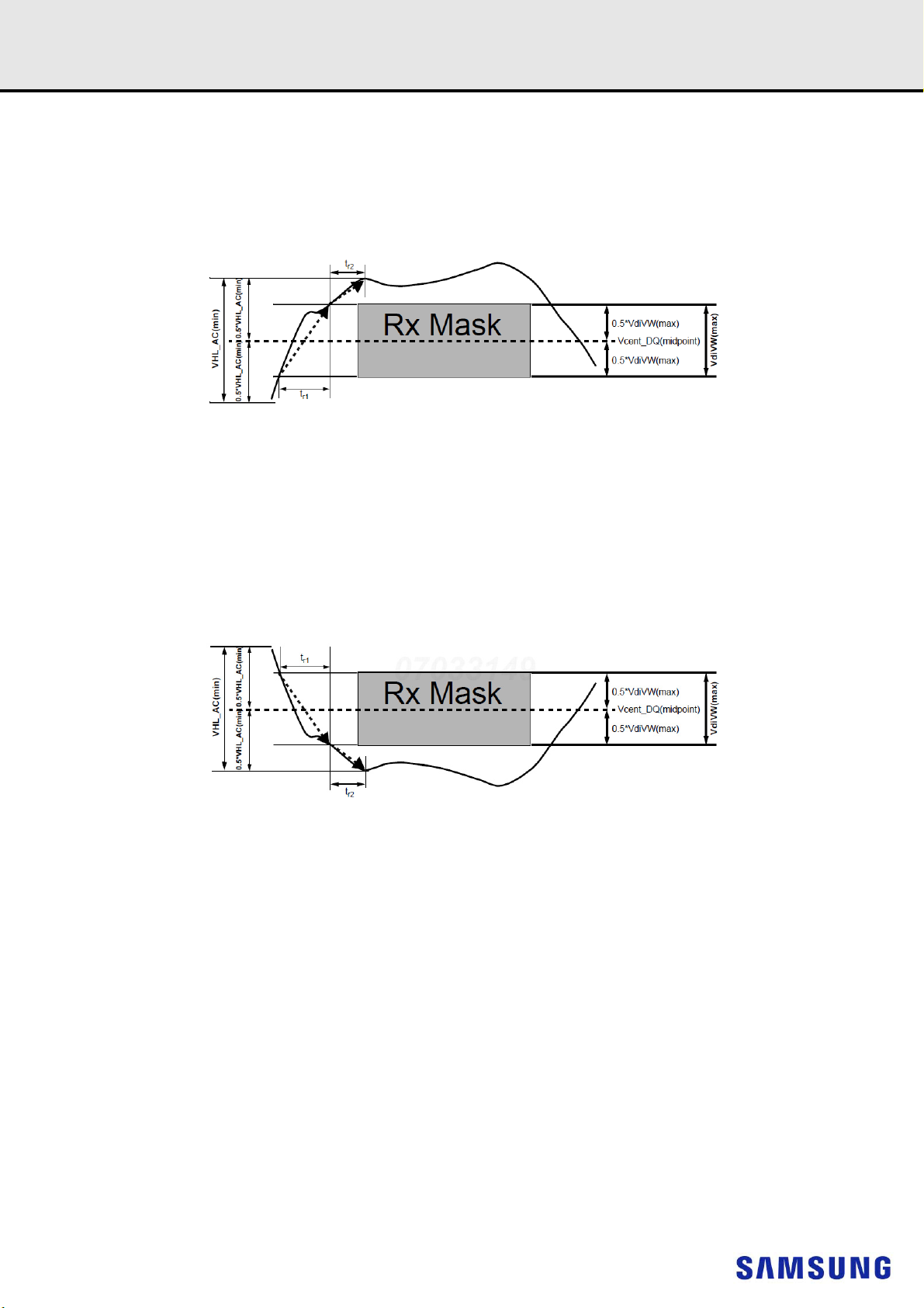
Rev. 1.3
Registered DIMM
The rising edge slew rates are defined by srr1 and srr2. The slew rate measurement points for a rising edge are shown in Figure 26 below: A low to high
transition tr1 is measured from 0.5*VdiVW(max) below Vcent_DQ(midpoint) to the last transition through 0.5*VdiVW(max) above Vcent_DQ(midpoint)
while tr2 is measured from the last transition through 0.5*VdiVW(max) above Vcent_DQ(midpoint) to the first transition through the 0.5*VIHL_AC(min)
above Vcent_DQ(midpoint).
Rising edge slew rate equations:
srr1 = VdIVW(max) / tr1
srr2 = (VIHL_AC(min) – VdIVW(max)) / (2*tr2)
Figure 26. Slew Rate Conditions For Rising Transition
The falling edge slew rates are defined by srf1 and srf2. The slew rate measurement points for a falling edge are shown in Figure 27 below: A high to low
transition tf1 is measured from 0.5*VdiVW(max) above Vcent_DQ(midpoint) to the last transition through 0.5*VdiVW(max) below Vcent_DQ(midpoint)
while tf2 is measured from the last transition through 0.5*VdiVW(max) below Vcent_DQ(midpoint) to the first transition through the 0.5*VIHL_AC(min)
below Vcent_DQ(pin mid).
datasheet
DDR4 SDRAM
Falling edge slew rate equations:
srf1 = VdIVW(max) / tf1
srf2 = (VIHL_AC(min) – VdIVW(max)) / (2*tf2)
Figure 27. Slew Rate Conditions For Falling Transition
- 73 -
Page 82

Rev. 1.3
Registered DIMM
datasheet
DDR4 SDRAM
19.3 Command, Control, and Address Setup, Hold, and Derating
The total tIS (setup time) and tIH (hold time) required is calculated to account for slew rate variation by adding the data sheet tIS (base) values, the
VIL(AC)/VIH(AC) points, and tIH (base) values, the VIL(DC)/VIH(DC) points; to the tIS and tIH derating values, respectively. The base values are
derived with single-end signals at 1V/ns and differential clock at 2V/ns. Example: tIS (total setup time) = tIS (base) + tIS.
For a valid transition, the input signal has to remain above/below VIH(AC)/VIL(AC) for the time defined by tVAC.
Although the total setup time for slow slew rates might be negative (for example, a valid input signal will not have reached VIH(AC)/ VIL(AC) at the time of
the rising clock transition), a valid input signal is still required to complete the transition and to reach VIH(AC)/ VIL(AC). For slew rates that fall between
the values listed in derating tables, the derating values may be obtained by linear interpolation.
Setup (tIS) nominal slew rate for a rising signal is defined as the slew rate between the last crossing of VIL(DC)max and the first crossing of VIH(AC)min
that does not ring back below VIH(DC)min. Setup (tIS) nominal slew rate for a falling signal is defined as the slew rate between the last crossing of
VIH(DC)min and the first crossing of VIL(AC)max that does not ring back above VIL(DC)max. Hold (tIH) nominal slew rate for a rising signal is defined as
the slew rate between the last crossing of VIL(DC)max and the first crossing of VIH(AC)min that does not ring back below VIH(DC)min. Hold (tIH) nominal
slew rate for a falling signal is defined as the slew rate between the last crossing of VIH(DC)min and the first crossing of VIL(AC)minthat does not ring
back above VIL(DC)max.
[Table 52] Command, Address, Control Setup and Hold Values
DDR4 1600 1866 2133 2400 2666 2933 Unit Reference
tIS(base, AC100) 115 100 80 62 - - ps VIH/L(ac)
tIH(base, DC75) 140 125 105 87 - - ps VIH/L(dc)
tIS(base, AC tbd) - - - - 55 48 ps VIH/L(ac)
tIH(base, DC tbd) - - - - 80 73 ps VIH/L(dc)
tIS/tIH @ VREF 215 200 180 162 145 138 ps
NOTE :
1) Base ac/dc referenced for 1V/ns slew rate and 2 V/ns clock slew rate.
2) Values listed are referenced only; applicable limits are defined elsewhere.
[Table 53] Command, Address, Control Input Voltage Values
DDR4 1600 1866 2133 2400 2666 2933 Unit Reference
VIH.CA(AC)min 100 100 100 100 90 90 mV VIH/L(ac)
VIH.CA(DC)min 75 75 75 75 65 65 mV VIH/L(dc)
VIL.CA(AC)max -75 -75 -75 -75 -65 -65 mV VIH/L(ac)
VIL.CA(DC)max -100 -100 -100 -100 -90 -90 mV VIH/L(dc)
NOTE :
1) Command, Address, Control input levels relative to VREFCA.
2) Values listed are referenced only; applicable limits are defined elsewhere.
- 74 -
Page 83
Rev. 1.3
Registered DIMM
[Table 54] Derating values DDR4-1600/1866/2133/2400 tIS/tIH - ac/dc based
10V/ns 8V/ns 6V/ns 4V/ns 3.0V/ns 2.0V/ns 1.5V/ns 1V/ns
∆tIS ∆tIH ∆tIS ∆tIH ∆tIS ∆tIH ∆tIS ∆tIH ∆tIS ∆tIH ∆tIS ∆tIH ∆tIS ∆tIH ∆tIS ∆tIH
7 765476557756795882608664947311189
6 735374537554775679588363927110888
5 705071517252745476568060886810585
4 654666476748695071527556836510081
CMD,
ADDR,
CNTL
Input
Slew
rate
V/ns
NOTE :
1) VIH/L(ac) = +/-100mV, VIH/L(dc) = +/-75mV; relative to VREFCA.
3 57405741584260446346675075589275
2 40284128422944314633503858467563
1.5 23 15 24 16 25 17 27 19 29 21 33 25 42 33 58 50
1-10-10-9-9-8-8-6-6-4-400882525
0.9 -17 -14 -16 -14 -15 -13 -13 -10 -11 -8 -7 -4 1 4 18 21
0.8 -26 -19 -25 -19 -24 -18 -22 -16 -20 -14 -16 -9 -7 -1 9 16
0.7 -37 -26 -36 -25 -35 -24 -33 -22 -31 -20 -27 -16 -18 -8 -2 9
0.6 -52 -35 -51 -34 -50 -33 -48 -31 -46 -29 -42 -25 -33 -17 -17 0
0.5 -73 -48 -72 -47 -71 -46 -69 -44 -67 -42 -63 -38 -54 -29 -38 -13
0.4 -104 -66 -103 -66 -102 -65 -100 -63 -98 -60 -94 -56 -85 -48 -69 -31
datasheet
∆tIS, ∆IH derating in [ps] AC/DC based
CK_t, CK_c Differential Slew Rate
DDR4 SDRAM
1)
[Table 55] Derating values DDR4-2666/2933 tIS/tIH - ac/dc based
∆tIS, ∆IH derating in [ps] AC/DC based
10V/ns 8V/ns 6V/ns 4V/ns 3.0V/ns 2.0V/ns 1.5V/ns 1V/ns
∆tIS ∆tIH ∆tIS ∆tIH ∆tIS ∆tIH ∆tIS ∆tIH ∆tIS ∆tIH ∆tIS ∆tIH ∆tIS ∆tIH ∆tIS ∆tIH
7 TBD TBD TBD TBD TBD TBD TBD TBD TBD TBD TBD TBD TBD TBD TBD TBD
6 TBD TBD TBD TBD TBD TBD TBD TBD TBD TBD TBD TBD TBD TBD TBD TBD
5 TBD TBD TBD TBD TBD TBD TBD TBD TBD TBD TBD TBD TBD TBD TBD TBD
4 TBD TBD TBD TBD TBD TBD TBD TBD TBD TBD TBD TBD TBD TBD TBD TBD
CMD,
ADDR,
CNTL
Input
Slew
rate
V/ns
NOTE :
1) VIH/L(ac) = +/-tbd mV, VIH/L(dc) = +/- tbd mV; relative to VREFCA
3 TBD TBD TBD TBD TBD TBD TBD TBD TBD TBD TBD TBD TBD TBD TBD TBD
2 TBD TBD TBD TBD TBD TBD TBD TBD TBD TBD TBD TBD TBD TBD TBD TBD
1.5 TBD TBD TBD TBD TBD TBD TBD TBD TBD TBD TBD TBD TBD TBD TBD TBD
1 TBD TBD TBD TBD TBD TBD TBD TBD TBD TBD TBD TBD TBD TBD TBD TBD
0.9 TBD TBD TBD TBD TBD TBD TBD TBD TBD TBD TBD TBD TBD TBD TBD TBD
0.8 TBD TBD TBD TBD TBD TBD TBD TBD TBD TBD TBD TBD TBD TBD TBD TBD
0.7 TBD TBD TBD TBD TBD TBD TBD TBD TBD TBD TBD TBD TBD TBD TBD TBD
0.6 TBD TBD TBD TBD TBD TBD TBD TBD TBD TBD TBD TBD TBD TBD TBD TBD
0.5 TBD TBD TBD TBD TBD TBD TBD TBD TBD TBD TBD TBD TBD TBD TBD TBD
0.4 TBD TBD TBD TBD TBD TBD TBD TBD TBD TBD TBD TBD TBD TBD TBD TBD
1)
CK_t, CK_c Differential Slew Rate
- 75 -
Page 84
Rev. 1.3
Registered DIMM
datasheet
DDR4 SDRAM
19.4 DDR4 Function Matrix
DDR4 SDRAM has several features supported by ORG and also by Speed. The following Table is the summary of the features.
[Table 56] Function Matrix (By ORG. V:Supported, Blank:Not supported)
Functions x4 x8 x16 NOTE
Write Leveling
Temperature controlled Refresh
Low Power Auto Self Refresh
Fine Granularity Refresh
Multi Purpose Register
Data Mask
Data Bus Inversion
TDQS
ZQ calibration
DQ Vref Training
Per DRAM Addressability
Mode Register Readout
CAL
WRITE CRC
CA Parity
Control Gear Down Mode
Programmable Preamble
Maximum Power Down Mode
Boundary Scan Mode
Additive Latency
3DS
VVV
VVV
VVV
VVV
VVV
VV
VV
V
VVV
VVV
VVV
VVV
VVV
VVV
VVV
VVV
VVV
VV
V
VV
VV
- 76 -
Page 85
Rev. 1.3
Registered DIMM
[Table 57] Function Matrix (By Speed. V:Supported, Blank:Not supported)
Functions
Write Leveling
Temperature controlled Refresh
Low Power Auto Self Refresh
Fine Granularity Refresh
Multi Purpose Register
Data Mask
Data Bus Inversion
TDQS
ZQ calibration
DQ Vref Training
Per DRAM Addressability
Mode Register Readout
CAL
WRITE CRC
CA Parity
Control Gear Down Mode
Programmable Preamble (= 2tCK)
Maximum Power Down Mode
Boundary Scan Mode
3DS
datasheet
DLL Off mode DLL On mode
equal or slower
than 250Mbps
VVVV
VVVV
VVVV
VVVV
VVVV
VVVV
VVVV
VVVV
VVVV
VVVV
VVVV
VVVV
DDR4 SDRAM
1600/1866/2133
Mbps
VVV
VVV
VVV
VVV
VVV
VVV
2400Mbps 2666/2933Mbps
V
VV
NOTE
- 77 -
Page 86
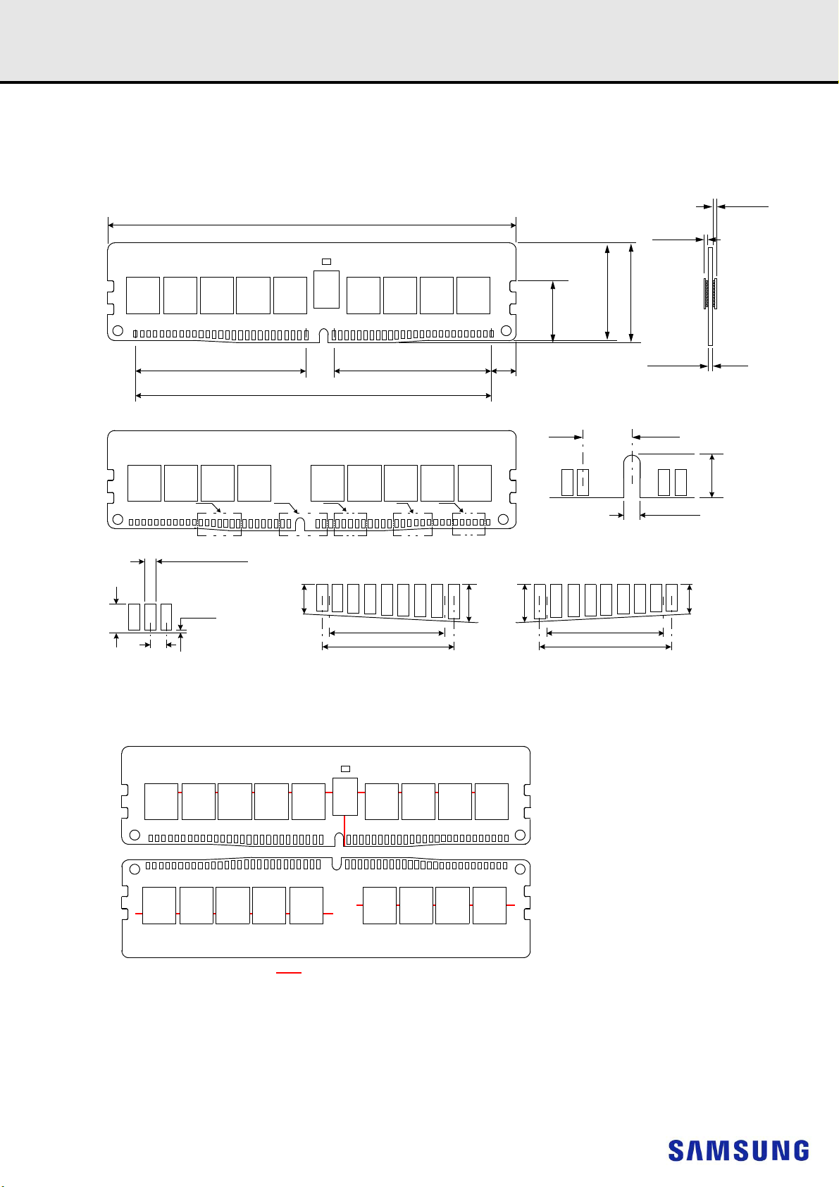
Rev. 1.3
133.35
Units : Millimeters
31.25
30.75
17.60
126.65
56.1064.60 3.35
A
C EDB
Detail A
1.50 ±
0.05
3.85 ±
0.10
4.30
0.85
0.25
E : 2.6
Detail B,E
0.6 ± 0.03
B : 2.1
Detail C
2.1
9.35
10.20
2.6
2.1
9.35
10.20
2.6
Detail D
1.4 ± 0.10
Max 1.4
Max 1.4
The used device is 1G x8 DDR4 SDRAM, Flip-Chip.
DDR4 SDRAM Part NO : K4A8G085WC-BC**
NOTE
:
1) Tolerances on all dimensions ±0.15 unless otherwise specified.
Address, Command and Control lines
U18U17U16U15U14U13U12U11U10
U1 U2 U3 U4 U5 U6 U7 U8 U9
datasheet
20. PHYSICAL DIMENSIONS
20.1 1Gx8 based 2Gx72 Module (2 Ranks) - M393A2K43CB1
DDR4 SDRAMRegistered DIMM
and M393A2K43CB2
20.1.1 2Gx72 DIMM, populated as two physical rank of x8 DDR4 SDRAMs
- 86 -
Page 87

Rev. 1.3
133.35
Units : Millimeters
0.85
0.25
E : 2.6
Detail B,E
Detail A
1.50 ±
0.05
0.6 ± 0.03
Detail C
31.25
30.75
17.60
126.65
4.30
B : 2.1
2.1
9.35
10.20
2.6
2.1
9.35
10.20
2.6
Detail D
56.1064.60 3.35
A
C EDB
3.85 ±
0.10
1.4 ± 0.10
Max 1.4
Max 1.4
The used device is 2G x4 DDR4 SDRAM, Flip-Chip.
DDR4 SDRAM Part NO : K4A8G045WC-BC**
NOTE
:
1) Tolerances on all dimensions ±0.15 unless otherwise specified.
Address, Command and Control lines
D18 D17 D16 D15 D10 D9 D8 D7 D6
D1 D2 D3 D4 D5 D11 D12 D13 D14
datasheet
20.2 2Gx4 based 2Gx72 Module (1 Rank) -
DDR4 SDRAMRegistered DIMM
M393A2K40CB1 and M393A2K40CB2
20.2.1 2Gx72 DIMM, populated as one physical rank of x4 DDR4 SDRAMs
- 87 -
Page 88

Rev. 1.3
Units : Millimeters
0.85
0.25
E : 2.6
Detail B,E
0.6 ± 0.03
Detail C
B : 2.1
2.1
9.35
10.20
2.6
2.1
9.35
10.20
2.6
Detail D
Detail A
1.50 ±
0.05
4.30
3.85 ±
0.10
1.4 ± 0.10
Max 1.4
Max 1.4
133.35
31.25
30.75
17.60
126.65
56.1064.60 3.35
A
C
D
E B
The used device is 2G x4 DDR4 SDRAM, Flip-Chip.
DDR4 SDRAM Part NO : K4A8G045WC-BC**
NOTE
:
1) Tolerances on all dimensions ±0.15 unless otherwise specified.
Address, Command and Control lines
D1 D2 D4 D5 D21 D22 D23 D24
D6 D7 D8 D9 D10 D25 D26 D27 D28
D32 D31 D30 D29 D15
D14
D13 D12 D11
D36 D35 D34 D33 D20 D19 D18 D17 D16
D3
datasheet
20.3 2Gx4 based 4Gx72 Module (2 Ranks) -
DDR4 SDRAMRegistered DIMM
M393A4K40CB1
20.3.1 4Gx72 DIMM, populated as two physical ranks of x4 DDR4 SDRAMs
- 88 -
Page 89
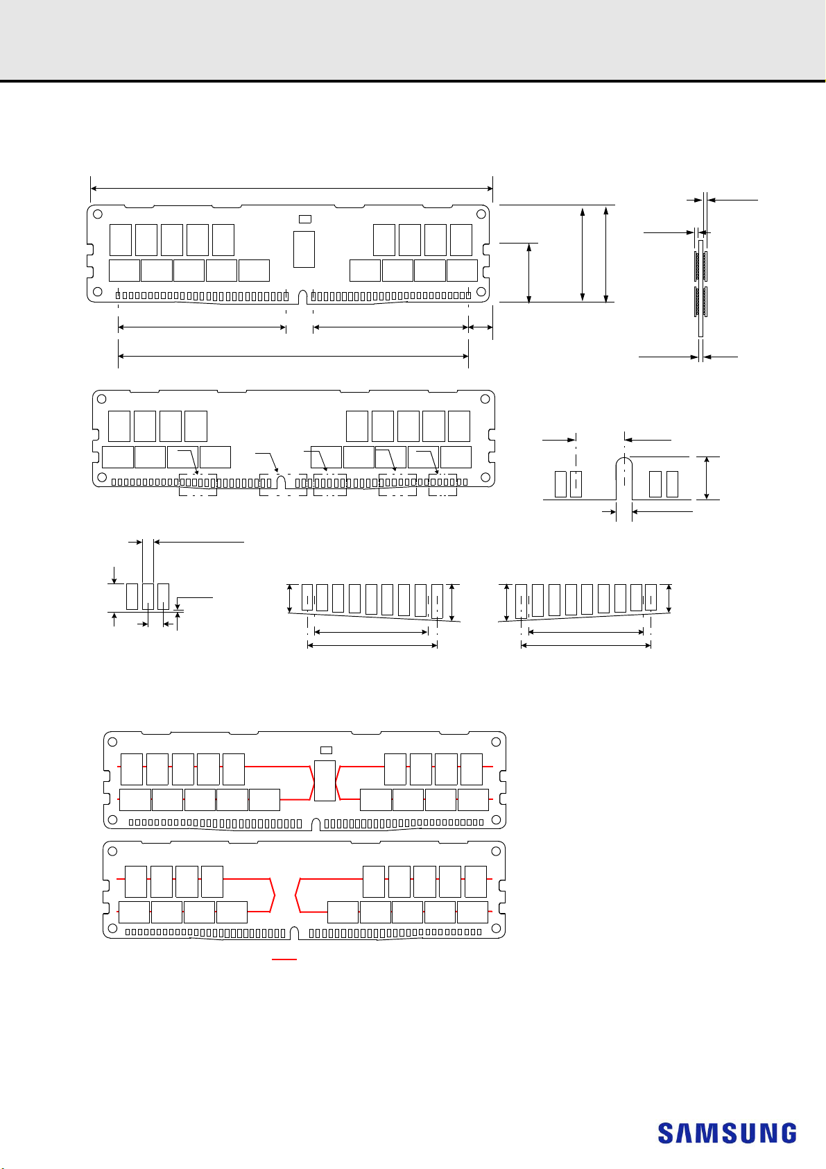
Rev. 1.3
Units : Millimeters
0.85
0.25
E : 2.6
Detail B,E
0.6 ± 0.03
Detail C
B : 2.1
2.1
9.35
10.20
2.6
2.1
9.35
10.20
2.6
Detail D
Detail A
1.50 ±
0.05
4.30
3.85 ±
0.10
1.4 ± 0.10
Max 1.4
Max 1.4
133.35
31.25
30.75
17.60
126.65
56.1064.60 3.35
A
C
D
E B
The used device is 2G x4 DDR4 SDRAM, Flip-Chip.
DDR4 SDRAM Part NO : K4A8G045WC-BC**
NOTE
:
1) Tolerances on all dimensions ±0.15 unless otherwise specified.
Address, Command and Control lines
D1 D2 D4 D5 D21 D22 D23 D24
D6 D7 D8 D9 D10 D25 D26 D27 D28
D3
D32D31D30D29 D15D14D13D12D11
D36 D35 D34 D33 D20 D19 D18 D17 D16
datasheet
20.4 2Gx4 based 4Gx72 Module (2 Ranks) -
DDR4 SDRAMRegistered DIMM
M393A4K40CB2
20.4.1 4Gx72 DIMM, populated as two physical ranks of x4 DDR4 SDRAMs
- 89 -
 Loading...