

Page 1

AllenBradley
Proportional/Inte
gral/Derivative
User
Control (2-Loop)
Module
(Cat.
No. 1771-PD)
Manual
Page 2

Table of Contents
Introduction 11. . . . . . . . . . . . . . . . . . . . . . . . . . . . . . . . . . . .
General 11. . . . . . . . . . . . . . . . . . . . . . . . . . . . . . . . . . . . . . . . . . .
Assembly and Installation 21. . . . . . . . . . . . . . . . . . . . . . . . .
General 21. . . . . . . . . . . . . . . . . . . . . . . . . . . . . . . . . . . . . . . . . . .
Hardware Description 21
Internal Selections 22
Manual
Control Station Interface
Input Power Supply Requirements 219
Installation Practices 222
Chassis Considerations 223
Internal Fusing 224
Recommendations for Installing or Removing Modules 224
Keying 225
Power Supply Specifications 227
Module
. . . . . . . . . . . . . . . . . . . . . . . . . . . . . . . . . . . . . . . . . . .
Specifications
. . . . . . . . . . . . . . . . . . . . . . . . . . . . . . . . .
. . . . . . . . . . . . . . . . . . . . . . . . . . . . . . . . . . .
217. . . . . . . . . . . . . . . . . . . . . . . . .
. . . . . . . . . . . . . . . . . . . . . . . .
. . . . . . . . . . . . . . . . . . . . . . . . . . . . . . . . .
. . . . . . . . . . . . . . . . . . . . . . . . . . . . . . .
. . . . . . . . . . . . . . . . . . . . . . . . . . . . . . . . . . . . . .
. . . . . . . . .
. . . . . . . . . . . . . . . . . . . . . . . . . . . .
229. . . . . . . . . . . . . . . . . . . . . . . . . . . . . . . . .
Programming 31. . . . . . . . . . . . . . . . . . . . . . . . . . . . . . . . . . .
General 31. . . . . . . . . . . . . . . . . . . . . . . . . . . . . . . . . . . . . . . . . . .
Operational Overview 32
Word
and Bit Definitions
Algorithm Flow Chart 351
Block Transfer Programming 351
Programming Considerations 370
Expanded Features 377
Programming Recommendations for Startup 388
. . . . . . . . . . . . . . . . . . . . . . . . . . . . . . . . .
38. . . . . . . . . . . . . . . . . . . . . . . . . . . . . . .
. . . . . . . . . . . . . . . . . . . . . . . . . . . . . . . . .
. . . . . . . . . . . . . . . . . . . . . . . . . . . .
. . . . . . . . . . . . . . . . . . . . . . . . . . .
. . . . . . . . . . . . . . . . . . . . . . . . . . . . . . . . . .
. . . . . . . . . . . . . . . .
Troubleshooting 41. . . . . . . . . . . . . . . . . . . . . . . . . . . . . . . .
General 41. . . . . . . . . . . . . . . . . . . . . . . . . . . . . . . . . . . . . . . . . . .
LED Troubleshooting Guide 41
Program Troubleshooting Guide 41
Calibration 51
General 51
Test
Preparation 52
Calibration Program 55
Calibration Procedures 59
. . . . . . . . . . . . . . . . . . . . . . . . . . . . . . . . . . . . . . . . .
. . . . . . . . . . . . . . . . . . . . . . . . . . . . . . . . . . . . . . . . . . .
Equipment
. . . . . . . . . . . . . . . . . . . . . . . . . . . . . . . . . . . . . . . .
. . . . . . . . . . . . . . . . . . . . . . . . . . . . . . . . . .
. . . . . . . . . . . . . . . . . . . . . . . . . . . .
. . . . . . . . . . . . . . . . . . . . . . . . .
51. . . . . . . . . . . . . . . . . . . . . . . . . . . . . . . . . . . . .
. . . . . . . . . . . . . . . . . . . . . . . . . . . . . . . .
Page 3

Table of Contentsii
Worksheets A1. . . . . . . . . . . . . . . . . . . . . . . . . . . . . . . . . . . .
Application Example 1, Continuous Block Transfer B1. . . . . .
General B1. . . . . . . . . . . . . . . . . . . . . . . . . . . . . . . . . . . . . . . . . . .
Example
Application
B1. . . . . . . . . . . . . . . . . . . . . . . . . . . . . . . . . .
Application Example 2, Periodic Block Transfer C1. . . . . . . . .
General C1. . . . . . . . . . . . . . . . . . . . . . . . . . . . . . . . . . . . . . . . . . .
Example
Application
C1. . . . . . . . . . . . . . . . . . . . . . . . . . . . . . . . . .
Summary Word and Bit Tables D1. . . . . . . . . . . . . . . . . . . . . .
Comparing ISA 1771PD Algorithms E1. . . . . . . . . . . . . . . . .
Algorithm Flow Chart F1. . . . . . . . . . . . . . . . . . . . . . . . . . . . .
Page 4

Introduction
Chapter
1
General
The Proportional/Integral/Derivation Control (2-loop) Module Assembly
(cat.no.1771-PD) is an intelligent I/O module that performs closed loop
PID control. The PID module is a process controller. The PID module
monitors the analog input process variable, compares the input to the
desired set point, and calculates the analog output control variable based
on the control algorithm programmed in the module. The PID module has
the hardware inputs and outputs and microprocessor to perform PID
control.
The PID module assembly consists of:
1 Proportional/Integral/Derivation Control (2-loop) Module (cat. No.
1771-PD)
1 Field Wiring Arm (cat. No. 1771-WF)
The PID module can control up to two closed loops such as flow,
temperature, pH, and level. Advanced control features include cascade,
feedforward, scaling, square root, error squared, digital and led/lag
filtering. The PID module can directly interface with an optional user
supplied manual control station. Transition from manual to automatic
control can be performed with bumpless transfer.
ranges can be selected for each loop to either +1 to +5V DC or +4 to
+20mA.
[1]
Input and output
The PC processor uses block transfer programming to communicate with
the module. The PC processor writes loop configuration parameters such
as gain constants, set points, digital filter values, limits, alarm points to
the PID module and reads status information such as analog input values,
analog output values, limit alarms and diagnostics from the PID module.
The PID module can be used with any Allen-Bradley PC processor that
has block transfer capability and uses the 1771 I/O structure.
When using the Mini-PLC-2 and PLC-2/20 processors, programming will
be more lengthy because these processors do not have the block format
instructions which permit shorter programs and easier data monitoring.
[1]
Bumpless
means a smooth transition from manual to automatic control.
transfer
, as defined in Fundamentals of Process Control Theory by Paul W
. Murril,
11
Page 5

Chapter 1
Introduction
Capabilities
The PID module can control one or two PID closed loops. The two loops
can be independent or linked together by and advanced control function
such as cascade or decoupling. Expanded loop features can be chosen in
addition to standard features to suite the application. All features are
software selectable with the exception of the I/O range, the source of +5V
DC, and the fault response to a hardware failure (which are selected using
internal programming plugs). Write block transfers to the module allow
program logic to enable the following features:
Standard features for input conditioning
detect the loss of process variable input
read the process variable at the PC processor
substitute a value from the PC processor for the process variable
take the square root of the process variable
\\digitally filter the process variable
Standard control features
select direct or reverse acting control
download a set point from the PC processor
limit and/or set an alarm on the error signal
download a dead band value from the PC processor
perform error dead band (zero crossing)
set an alarm when the error exceeds the dead band
select the control mode: proportional only, integral only, proportional
and integral, proportional and derivative, or all three
select error or error squared conditioning of the proportional and/or
integral error
select whether the derivative function operates on the error or the
process variable
set an alarm on the proportional term
limit and/or set an alarm on the integral term
limit and/or set an alarm on the derivative term
Standard features for output conditioning
limit and/or set an alarm on the PID algorithm output
read the PID algorithm output at the PC processor
download an output value from the PC processor
interface directly with a manual control station (bumpless transfer)
hold the PID algorithm output for independent loop tuning
hold the bias/feed forward term for independent loop tuning
12
Page 6

Chapter 1
Introduction
download an output bias from the PC processor
Expanded control features
perform scaling on the process variable, set point and/or error
set minimum and maximum scaling values
use the tieback as the feedforward input
take the square root of the feedforward input
add a feedforward offset
multiply the feedforward term by a constant
perform lead/lag filtering on the feedforward term
download a feedforward value from the PC processor
cascade the output of loop 1 into the set point of loop 2
decouple the VPID output of loop 1 into the feedforward input of loop
2
These features including integral term anti-reset wind-up are described in
chapter 3.
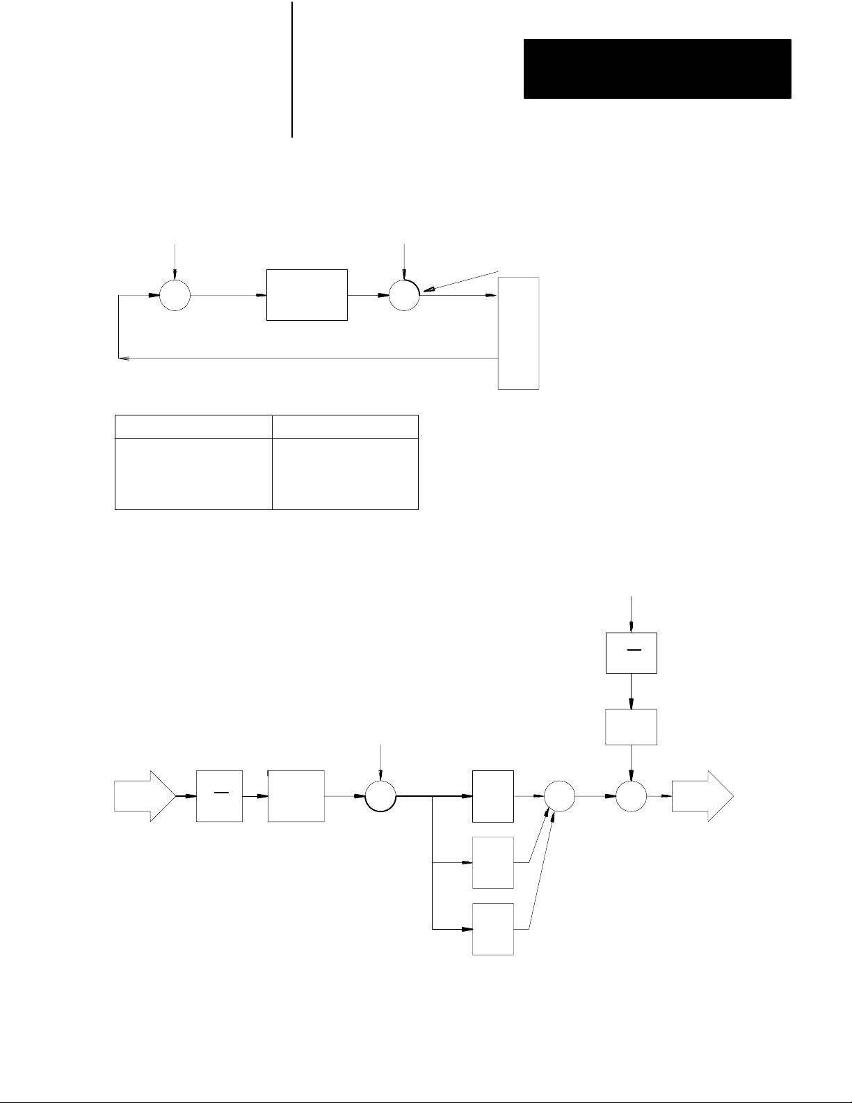
PID Algorithm
An algorithm is a step-by-step procedure. The purpose of the PID
algorithm is to maintain the process at the desired setpoint. A diagram of
PID closed loop control is shown in Figure 1.1a.
The PID module has many features. Select only those features that are
required for the particular application. Major control functions are shown
in Figure 1.1b. Refer to figure 3.15 for a detailed algorithm flow chart.
This flow chart shows the relationship of the user-selectable features.
PID modules (rev C or later) let you select the ISA or Allen-Bradley
algorithm. Refer to appendix E for a comparison of algorithm values.
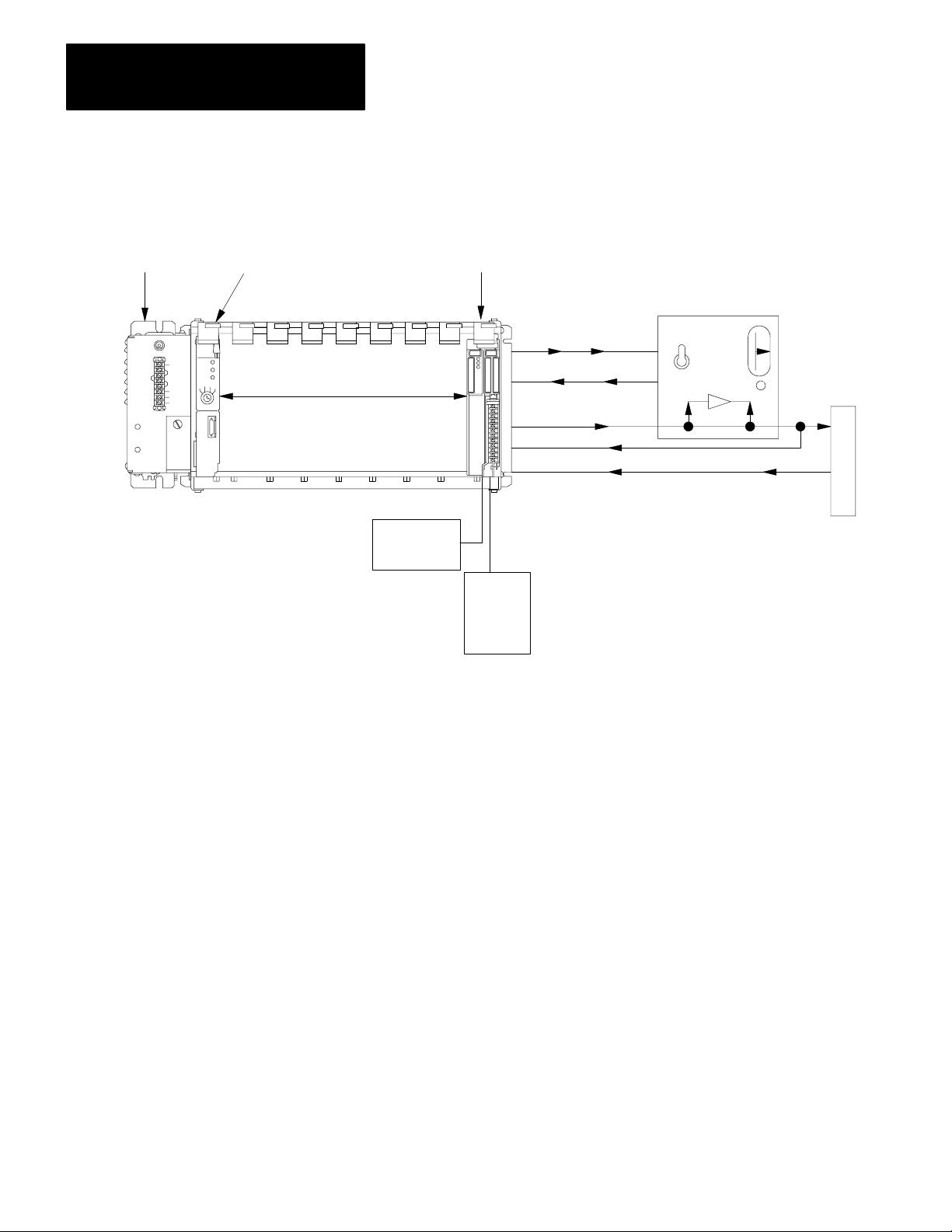
Hardware Description
The PID module has four analog inputs and two analog outputs each with
12-bit binary resolution. Each input and output can be individually
selected to either the +4 to +20mA or +1 to +5V DC range without
recalibration. The selection is made with internal programming plugs.
Each loop has one process variable input, one tieback input and one
analog output associated with it. The tieback analog input is used to track
the analog output of the manual control station to permit bumpless
transfer. Each loop uses one discrete input to track the status of the
optional manual control station. A contact output is used to switch the
13
Page 7

Chapter 1
Introduction
manual control station of both loops to manual control. The module’s
analog inputs can be read and outputs can be set by the PC processor.
The PID module can draw its +5V DC operating power from either the
chassis backplane power supply or from a user-supplied +5V DC power
supply through the field wiring arm. The external power supply option
permits a more fault tolerant system by allowing the PID module to be
powered independently. The PID module also requires +15V DC power
for the analog circuitry.
Typical PID hardware and signal paths are shown in Figure 1.2.
14
Page 8
Chapter 1
Introduction
SP
+
-
PV
S
Error=SP-PV
PV = Process Variable
SP = Set Point
AB ISA
V = Control Variable
= Proportional Term K
V
P
VI = Integral Term K
VD = Derivative term K
Figure 1.1
Simplified
VP + VI + V
Control Variable
P
I
D
Controller Gain K
Reset Term 1/
Rate Term T
PID Algorithm
D
C
Ti
d
BIAS
+ VI + V
V = V
+
P
D +
BIAS
+
S
P
r
o
c
e
s
s
a) PID Closed Loop Control
Process
Variable
A/D
/
Hardware
Analog
Input
b) Major Control Functions
Digital
Filter
PV
SP
+
Error=SP-PV
S P
Feedforward Input
/
Lead
Lag
BIAS
V
PID
SS
V
I
D
(FFV)
Control Variable
D/A
Hardware
Analog
Output
11099
15
Page 9
Chapter 1
Introduction
Figure 1.2
Overview
System
1771 –P1
Supply
PC Processor
or Adapter
Block Transfer
1770 –P1 supply
+
15V DC
–
100mA
1771 –PD
Module
+5V DC
1.2A
Optional
Supply
Manual Request
Man/Auto Status
Analog Output (V)
Analog Input (PV)
Optional
User Supplied
Manual Control Station
Tieback Input
X
P
r
o
c
e
s
s
11092
16
Programming Description
The PID algorithm can be adapted to the particular control application by
selecting desired features. The features and parameter values are chosen
and stored in the PC processor data table. The PC processor transfers to
the PID module data table blocks which contain the feature selections and
parameter values. The module uses the values to establish its operational
characteristics. The PC processor can read the module status by
transferring information from the module into the data table.
Communication between PC processor and PID module is performed by
block transfer programming.
Levels of Fault Tolerance
The module has five levels of fault tolerance.
The first level occurs when the PID module is operating properly but a
loss of communication with the active PC processor occurs. The module
enters a mode of operation defined as soft fault. A soft fault occurs when:
Page 10

Chapter 1
Introduction
PC processor operation is changed from run mode to program or
test mode
a PC processor fault occurs
a communications cable break occurs between the PC processor
and the I/O chassis
Each loop can be programmed independently to one of the following
responses when a soft fault occurs:
set the analog output to minimum value (+4mA or +1V DC)
holds the analog output to the last value before the soft fault occurre
performs PID control based on the last values transferred to the module
before the soft fault occurred.
sets the analog output to maximum value (+20MA or +5V DC)
The second level of fault tolerance is how the module sets its outputs in
response to a hard fault. A hard fault occurs when the module detects a
failure of its microprocessor or its self-diagnostics. Internal programming
plugs are used to select the manner in which the PID module can respond
if a hard fault should occur:
sets analog output to minimum value (+4MA or +1V DC)
holds analog outputs at the last value before the fault occurred
sets analog outputs to maximum value (+20mA or +5V DC)
Note: These hard fault responses cannot be ensured if a component in the
analog output circuit should fail.
A manual control station can be connected between the PID module
analog output and the controlled element of the process. Control of the
output can be switched manually to the manual control station by a switch
at the station. Manual control at the station overrides the PID module’s
output.
The third level of fault tolerance is automatic switching of control to the
manual control station when a hard fault occurs. A relay contact in the
PID module closes automatically (manual request), putting the station in
control. The module’s output is overridden by the station output.
The fourth level of fault tolerance is the module’s response to loss of +5V
DC. Outputs respond as if a hard fault occurred (a or C above, but not b).
The same programming plug configuration selects the module’s response.
If +15V DC is lost, analog outputs go to minimum value, regardless.
17
Page 11

Chapter 1
Introduction
The last level of fault tolerance results from powering the module from
external +5V DC and +
l5V DC power supplies, independent of I/O
chassis backplane power, through the field wiring arm.
Application in Control Systems
The PID module performs closed loop control. Once programmed, it can
operate independently of the PC processor. System status and alarm
information can be reported to the PC processor to ensure safe system
performance.
Redundant control is another alternative. PID modules could serve as
back-up to a PC processor performing the PID loop algorithms. The PC
processor can control many complex and interaction loops using PID
modules for analog inputs and outputs. The complex algorithm could be
subdivided into individual loop algorithms stored in the PID modules
operating as analog I/O modules. In the event of a PC processor failure or
loss of communication between PC processor and a PID module, the soft
fault mode of the PID module would allow it to automatically control its
loops according to the PID loop algorithms stored in its memory if the
appropriate soft fault response had been selected.
18
Page 12
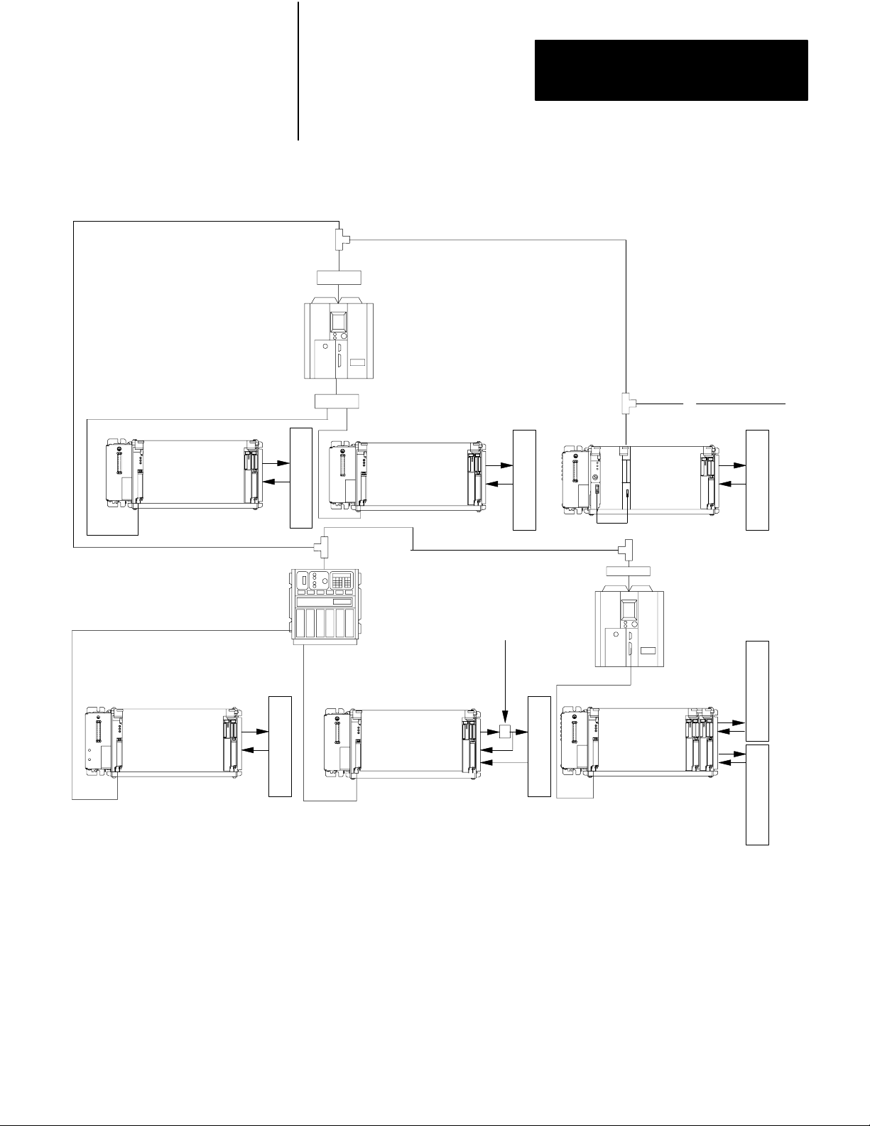
Figure 1.3
of Distributed Control
Levels
Chapter 1
Introduction
Data Highway
1771 - PD
1771 - PD
P
r
o
c
e
s
s
P
r
o
c
e
s
s
1771 - PD
1771 - PD
P
r
o
c
e
s
s
Manual Control
Station
P
r
o
c
e
s
s
1771 - PD
1771 - PD
P
r
o
c
e
s
s
P
r
o
c
e
s
s
P
r
o
c
e
s
s
11100
The PID module can also be used in a system with adaptive control based
on the PC processor’s ability to constantly adjust the control algorithm in
the module.
19
Page 13

Chapter 1
Introduction
Finally, PID modules can be used in distributed control schemes. The
data highway can be used to link PC processors which are controlling PID
modules. Figure 1.3 shows the various levels of distributed control.
Manual Overview
The remainder of the manual explains different aspects of PID module
operation.
Chapter 2 - Assembly and Installation contains hardware information
including wiring diagrams, programming plug selection of I/O ranges
and compliance, installation and keying, wiring diagrams and
specifications of the PID module and power supplies.
Chapter 3 - Programming contains detailed explanations of all the
software selectable features.
Chapter 4 - Troubleshooting contains helpful troubleshooting
information.
Chapter 5 - Calibration presents the procedure for recalibrating the PID
module.
Appendix A contains recots which are helpful when selecting features
and programming the module.
Appendices B and C provide sample ladder diagram programs based on
sample applications.
Appendix D contains summaries of value words and control bits used
when programming.
Appendix E shows how to convert ISA standard values to 1771-PD
gain values.
Appendix F is an enlarged algorithm flow chart for your convenience.
110
Page 14
Chapter
Assembly and Installation
2
General
Hardware Description
The PID module must be configured internally and wired externally to
suite the conditions under which the module will be used. Module and
power supply specifications are listed at the end of this chapter.
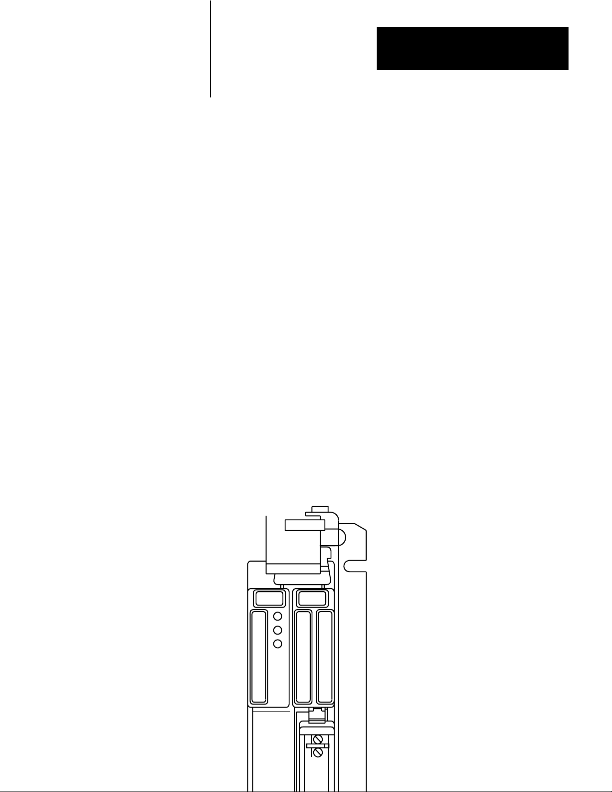
The PID module is a dual-slot module. The left front panel contains three
LED indicators, the right front panel contains a write-on label that can be
used to record the voltage or current range and the most recent date of
calibration. An 18 terminal field wiring arm is connected to the lower
right front of the module for I/O and power connections. The label on the
right cover plate identifies the terminals of the field wiring arm.
Diagnostic Indicators
Front panel indicators (Figure 2.1) allow an operator to observe the
operating condition of the module. The indicators will be on, off or
flashing (Table 2.A).
Figure 2.1
Diagnostic
Indicators
FAULT
RUN
STAND
ALONE
21
Page 15

Chapter 2
Assembly and Installation
Table 2.A
Indicator
Indicator State Condition
FAULT
(red)
RUN
(green)
STAND
ALONE
(yellow)
OFFONNormal operation.
ON
Flashing
OFF
Toggle
OFF
Flashing
Diagnostics
Hardware fault. Analog outputs are held at either last
state, minimum or maximum value as determined by the
userselected programming plugs. If this indicator is on,
the other indicators are not valid
Normal operation
PID module is initially powered (unprogrammed and is
waiting for data from the PC processor
PID module is not in the normal run mode.
Analog power (+
and RUN indicators are alternately toggling on and of
Normal operation
The module is in soft mode and is controlling PID loops
independently
Processor.
15V dc) is lost when ST
. It is not communicating with an active PC
.
AND ALONE
f.
NOTE: All indicators are of
Internal Selections
NOTE: Disconnecting the field wiring arm will interrupt
PID control.
Toggle
ON
Analog power (+
and RUN indicators are alternately toggling on and of
A programming error is causing a block transfer
communication error
f when in calibration mode.
15V dc) is lost when ST
.
AND ALONE
f.
In order to accommodate a wide variety of applications, a number of
programming (jumper) plugs must be correctly positioned inside the PID
module. The following functions are user-selectable using the
programming plugs:
output range: +4 to +20mA or +1 to +5V dc
input range: +4 to +20mA or +1 to +5V dc
tieback input range: +4 to +20mA or +1 to +5V dc, if used current
output compliance: standard or additional hard fault output: hold last
value or max/min value output for loss of +5V dc: max or min value
+5V dc source: backplane or external
22
Page 16

Chapter 2
Aseembly and Installation
Calibration of the I/O ranges should be checked yearly to maintain
specified accuracy.
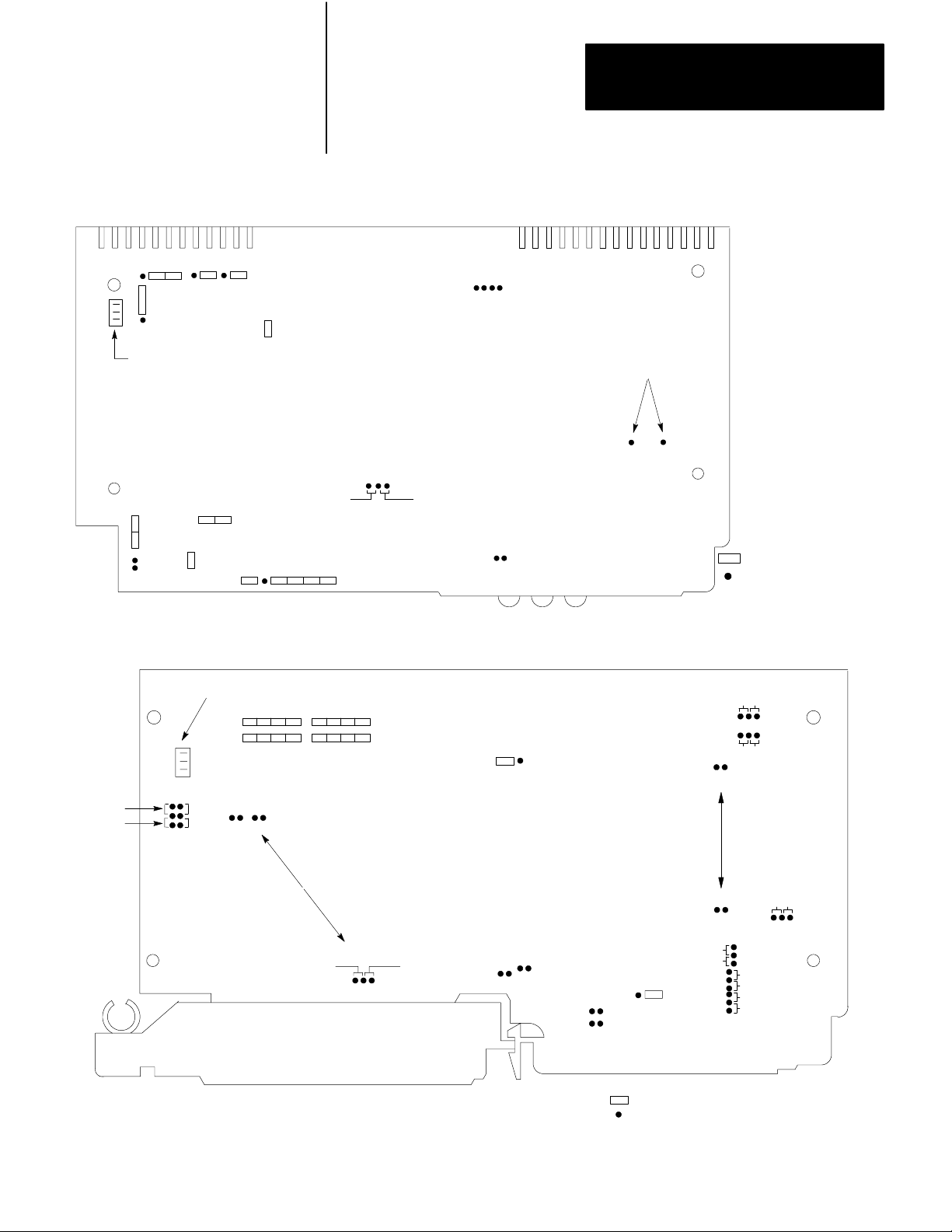
Programming Plugs and Locations
The PID module contains two printed circuit boards. The left-hand board
is the digital board, the right-hand board is the analog board.
Programming plugs are located on both the analog and digital circuit
boards inside the PID module. Typically they stand higher than the
surrounding components on the circuit board. The programming plug
locations are labeled E1 through E24 on the analog board. The only
user-selectable programming plugs on the digital board are E2 and E10.
Some of the programming plug locations are factory configured and must
remain in the configuration except during calibration. They are called out
as factory configured in the programming plug position tables and in the
figures which show their locations.
User-selectable plug locations have either two or three pins per plug.
Programming plugs electrically connect two pins. The plug can be placed
over the required pins or stored by placing the plug over a single pin,
electrically floating.
Programming Plug Selection
Programming plugs should be set with care after decisions are made
which govern their placement. The following procedure will be helpful to
ensure that all the programming plugs are properly set. The procedure
consists of 5 parts.
a. Select digital board features. Record features on Table 2.B
b. Select analog board features. Record features on Table 2.C.
c. Record the position on analog plugs by completing Table 2.D.
d. Set programming plugs on the digital board using Table 2.B.
e. Set programming plugs on the analog board using Table 2.D.
23
Page 17

Chapter 2
Assembly and Installation
Selection Procedure (Part A)
Begin with digital board features using Table 2.B.
1. The hard fault response of the module is selected first. A hard fault
occurs when a module failure is detected in the event of a failure, the
analog output will either maintain the last value or will be set to the
minimum or maximum value. A single choice is made for both
outputs as to whether they hold last value or go to
minimum/maximum.
Select hold last value or go to minimum/maximum for the hard fault
response. Record your selection on Table 2.B by circling RIGHT for hold
last value or LEFT for minimum/maximum.
NOTE: If hold last value is selected for hard fault, output 1 and output 2
must still be selected for minimum or maximum. The selection
determines the state of outputs at module power-up (green LED flashing)
until the load/enter sequence is complete, or power-down of +5V dc. See
Table 2.C.
Table 2.B
Programming
E1
E2
[1]
E3 through E9
E10
[1]
The selection for E2 affects both outputs the same. The choice of minimum value or maximum
value for the hard fault output must be made on the analog board regardless of the choice of
E2. (see text and analog board plugs E4 and/or E5).
Plug Selections: Digital (lefthand) Board
Location Function Position
Factory Configured
Hard fault response:
Hold last value
Minimum/maximum value
Factory Configured
Source of +5V dc
Backplane
External supply
OUT
RIGHT
LEFT
See figure 22
IN
OUT
24
Page 18

Chapter 2
Aseembly and Installation
Table 2.C
Programming Plug Selections: Analog (righthand) Board
Choose and record the required conditions for each function below.
Function Condition
Output
1: Hard Fault
or Loss of +5V dc
Output 2: Hard Fault
or Loss of +5V dc
Analog Input 1
Analog Output 1
T
ieback Input 1
Analog Input 2
Analog Output 2
T
ieback Input 2
Compliance
Source of +5V dc
Minimum V
Maximum V
Minimum V
Maximum V
Voltage
Current
Voltage
Current
Voltage
Current
Voltage
Current
Voltage
Current
Voltage
Current
Standard (500 ohms: COMMON @ OV)
Additional (1250 ohms: COMMON @ 15V)
Backplane
External Supply
alue
alue
alue
alue
25
Page 19

Chapter 2
Assembly and Installation
Table 2.D
Programming Plug Positions: Analog (righthand) Board
Mark the programming plug position for each function below.
Location Function Position
E1 Output
Output 2, voltage mode
E2
E3
E4
E5
E6
E7
E8
E9
E11 T
Output 2, current mode
Output 2, voltage mode
Output 1, current mode
Output 1, voltage mode
Hard fault* output 2, minimum
Hard fault* output 2, maximum
Hard fault* output 1, to minimum
Hard fault* output 1, to maximum
Output 1, voltage mode
Output 1, current mode
Output 2, voltage mode
Output 2, current mode
Output 1, voltage mode
Output 2, current mode
Factory configured
ieback 1, current mode
T
ieback 1, voltage mode
2, current mode
LEFT
RIGHT
LEFT
RIGHT
LEFT
RIGHT
IN
OUT
IN
OUT
TOP
BOTTOM
TOP
BOTTOM
TOP
BOTTOM
RIGHT
IN
OUT 1
26
E12 T
E13
E14
E15
E16,17
E18
[2]
E19, 20 Factory configured
E21
[2]
E22[ 2 ]
ieback 2, current mode
T
ieback 2, voltage mode
Factory configured
Input 2, current mode
Input 2, voltage mode
Input 1, current mode
Input 1, voltage mode
Factory configured
Additional compliance (15V dc)
Standard compliance (OV dc)
Additional compliance
Standard compliance
Additional compliance
Standard compliance
IN
OUT 1
LEFT
IN
OUT 1
IN
OUT 1
BOTH IN
LEFT
RIGHT
BOTH IN
OUT 1
IN
OUT [1]
IN
Page 20

Chapter 2
Aseembly and Installation
Location PositionFunction
E23
[3]
E24
[3]
*or loss of +5V dc
[1]
IN refers to connecting the two pins together. OUT refers to storing the programming plug by
placing it over a single pin, electrically floating.
[2]
The positions of programming plugs E18, E21 and E22 must be the same.
[3]
The positions of programming plugs E23 and E24 must be the same.
NOTE
: Use figure 2.3 to locate the programming plugs.
+5V dc from backplane
+5V dc from external source
+5V dc from backplane
+5V dc from external source
TOP
BOTTOM
TOP
BOTTOM
2. Select source of +5V dc as the backplane or external supply. Record
your selection on Table 2.B by circling IN for backplane or OUT for
external.
Part B)
Select and record the analog board features on Table 2.C using the
following procedure.
Select the modules’ response to a hard fault or loss of +5V dc. Choose
maximum or minimum value for either output 1 or 2. Make these
selections regardless of how you set E2 in Table 2.B. If you selected hold
last value, you still must select maximum or minimum value for each
output. Outputs go to the selected value at module power-up (green LED
flashing) until the load/enter sequence is complete, or when powering
down +5V dc.
1. Choose minimum or maximum response of output 1 for hard fault or
power-down of +5V dc.
2. Choose minimum or maximum response of output 2 for hard fault or
power-down of +5V dc.
3. Choose analog input 1 as either voltage mode (+1 to 5V dc) or
current mode (+4 to +20mA).
4. Choose analog output 1 as voltage or current.
27
Page 21

Chapter 2
Assembly and Installation
5. Choose the tieback input 1 as voltage or current.
If tieback input 1 is wired to track the manual control station associated
with analog output 1, then both tieback input 1 and analog output 1 must
be selected to the same mode of either current or voltage.
6. Choose analog input 2 as voltage or current.
7. Choose analog output 2 as voltage or current.
8. Choose tieback input 2 as voltage or current.
If tieback input 2 is wired to track the manual control station associated
with analog output 2, then both tieback input 2 and analog output 2 must
be selected to the same mode of current or voltage.
9. Choose compliance as standard or additional.
Compliance is defined as the maximum allowable load impedance in the
current mode. The standard compliance for the PID module is 500 ohms.
Additional compliance can be established for one or two loops, only if
analog outputs 1 and 2 and tieback inputs 1 and 2 are all selected for the
current mode.
(The condition on tieback inputs is required only when they are tracking
outputs.) Additional compliance allows a maximum load impedance of
1250 ohms. Additional compliance is obtained by internally referencing
the MODULE COMMON terminal to the -15V dc terminal. Choose
standard or additional compliance and record in Table 2.C. The choice
may affect the power supply requirement for input devices as described in
section titled External Connections.
10.Choose the source of +5V dc as either the backplane or external
supply.
11.Review all the choices made in table 2.C before continuing.
28
Page 22

Chapter 2
Aseembly and Installation
Part C)
Record the required programming plug positions on table 2.D using your
selections on table 2.C for reference. Select LEFT/RIGHT, IN/OUT or
TOP/BOTTOM so that Table 2.D has a position defined for every E
location.
1. Using your selections inTable 2.C for reference, mark the
corresponding plug positions in the right-hand column of Table 2.D
Table 2.D. For example, if the required condition for output is
minimum value due to hard fault or loss of +5V dc, mark the IN
position in Table 2.D for E5.
Part D)
Set programming plugs E2 and E10 on the digital board using Table 2.B
and the following procedure:
1. Remove the unmarked left cover plate to gain access to the digital
circuit board.
2. Refer to Figure 2.2 to identify the location of the user-selectable and
factory configured programming plugs.
3. Set programming plugs E2 and E10 according to the functions
circled in Table 2.B.
4. Verify that the factory configured programming plugs are installed as
shown in Figure 2.2
5. Set the completed digital board, cover, and screws to one side.
Part E)
Set the programming plugs on the analog board usingTable 2.D and the
following procedure:
1. Remove the right cover (with the terminal identification label) to
gain access to the analog circuit board.
29
Page 23

Chapter 2
Assembly and Installation
2. Refer to Figure 2.3 to identify the locations of the user-selectable and
factory configured programming plugs.
3. Starting at E1, read down table 2.D and set each programming plug
on the analog board.
CAUTION: The programming plugs at location E11 and E12
could interfere with the front cover flange when the analog
board is re-assembled to the rest of the module. This could
happen when either the E11 or E12 programming plug is placed
in the OUT (floating) position. When either is required to be in
the OUT position, place the floating side of the E11 plug toward
the center of the board and the floating side of the E12 plug
toward the top of the board.
4. Verify that factory configured programming plugs are in their correct
positions.
5. Re-assemble the PID module. Typically it is easier to re-assemble
the digital board and cover before the analog board and cover.
Observe caution when re-assembling the analog circuit board. Be
certain that the three stake pins located on the lower corner of the
board mate with their respective sockets on the digital board.
Carefully align these connections before aligning and tightening the
screws on the module cover.
Record the I/O range selections on the module’s write-on label.
210
Page 24
Chapter 2
Aseembly and Installation
Backplane Connector
*
E6
StakePin
Connector
*
E8
E9
Figure 2.2
Programming
*
E5
E4
Hold
Max
*
E7
*
Min
E3
*
Plug Locations (Digital Board)
Backplane Connector
*
E1
No
Plug
Hold
Last
State
E10
Diagnostic Indicators
Jumper
Test
Pins
Programming Plug
Pin
*
Factory Configured Plug
11101
Backplane
External
E24E
Stake Pins
E19
E
20
23
*
*
E22E
IN or Out
21
Figure 2.3
Programming Plug Locations (Analog Board)
*
E1
6
*
E
7
Additional
(-15V dc)
Compliance
E18
1
Standard
(0V dc)
E
13
IN or OUT
E14
*
E15
IN or OUT
E11
E12
E9
VI
E1
E2
I
V
E4
IN or OUT
IN or OUT
E5
*
E8
E6
V
V
I
V
E3
I
I
Plug
n
Pi
Factory Configured
*
11096
211
Page 25

Chapter 2
Assembly and Installation
External Connections
Terminal identification of the PID module’s field wiring arm and general
connections are shown in Figure 2.4. Typical I/O connections for a single
closed loop configured in current mode are shown in Figure 2.5. The
remaining three figures show typical connections to input and output
devices and control mode connections to a manual control station.
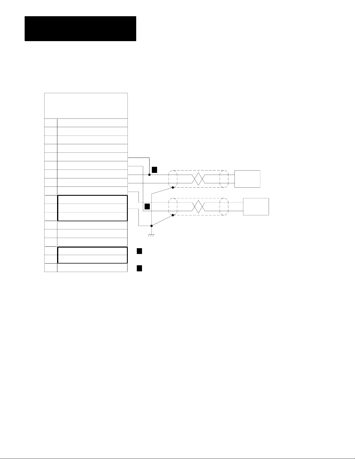
Figure 2.6 shows typical connections to input devices without a manual
control station. When an input loop is configured in current mode, the
input impedance of all devices connected in series must be considered
when selecting the input power supply. the input loop could contain one
or more recording devices (250 ohms) and/or a manual control station
(100 ohms) in addition to the PID module (250 ohms) and the current
transmitter. Current transmitters typically require at least 18V dc.
Voltage transmitters, if used, draw their power from a supply independent
of the input circuit.
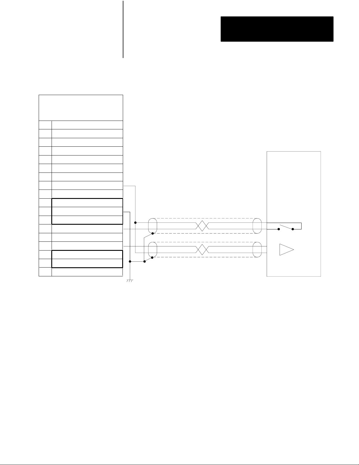
Figure 2.7 shows typical connections to actuators when the output is
monitored by the tieback input. Note that when a tieback input is not used
to monitor a voltage output, the jumper to the TIEBACK INPUT terminal
is not connected. When the tieback input is not used to monitor a current
output, the return from the actuator is connected to MODULE
COMMON, not to the TIEBACK INPUT terminal. The module monitors
tieback inputs only when you enable manual mode of the manual control
station described below.
Figure 2.8 shows the connections from the PID module to a manual
control station required for switching control automatically to the station
or manually at the station. The wiring is the same for PID module outputs
configured in current or voltage mode.
The MANUAL REQUEST terminal permits the PID module, upon
detecting a hard fault or when under PC processor control, to switch the
manual control station from automatic to manual mode. The MANUAL
MODE terminal is used to inform the PID module when the station is in
manual mode. The TIEBACK INPUT terminal monitors the station
output and allows a bumpless transfer of control from the manual control
station to the PID module.
212
Page 26
Chapter 2
Aseembly and Installation
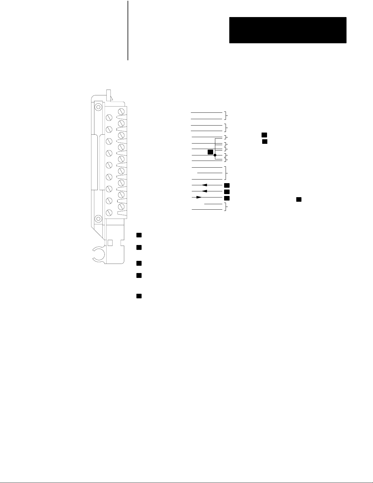
Figure 2.4
Terminal
Terminal Identification
Terminal Function
18
17
16
15
14
13
12
11
10
9
8
7
6
5
4
3
2
1
18 Input 1 (+ Lead)
17 Input 1 (- Lead)
16 Input 2 (+ Lead)
15 Input 2 (- Lead)
14 Tieback Input 1
13 Tieback Input 2
12 Analog Output 1
11 Module Common
10 Analog Output 2
9 +15V DC
8 15V DC Common
7 -15V DC
6 Manual Mode 1
5 Manual Mode 2
4 Manual Request
3OPT.+5VDCCommon
2 Optional +5V DC
1 Not Used
1
The tieback inputs can be used to track manual control station output to provide bumpless
transfer, or can be used as feedforward inputs.
2
Module common signal level can be selected to either 15V DC COMMON (system
common) for standard compliance, or -15V DC for additional compliance depending
on the application.
3
When the manual control station is in manual, the station switches these line to the
MODULE COMMON terminal.
4
When a request for manual is made from the PID module or when this relay contact output
is used for alarm annunciation, the line is switched to the module common signal level for
50 msec. For hardware failure or loss of analog power ( 15V DC), this relay output is held
at module common until the fault is corrected.
5
Programming plugs must be positioned for optional + 5V DC supply.
Identification and Connections
Cat. No. 1771-PDC
2
+
-
Process Variable 1
Process Variable 2
Process Variable 2Process Variable 2
Tieback Input 1
Tieback Input 2
1
1
Control Element 1
Module Common
Control Element 2
Required +15V DC Power Supply
(cat. no. 1770-P1, 1778-P2, or equivalent)
3
3
4
Optional +5V DC Power Supply
5
(cat. no. 1771-P2 or equivalent)
+
-
+
-
11097
213
Page 27
Chapter 2
Assembly and Installation
PID Module
TERMINAL IDENTIFICATION
CAT. NO. 1771-PDC
TERMINAL FUNCTION
INPUT 1 (+LEAD)
18
INPUT 1 (-LEAD)
17
INPUT 2 (+LEAD)
16
INPUT 2 (-LEAD)
15
14
TIEBACK INPUT 1
13
TIEBACK INPUT 2
ANALOG OUTPUT 1
12
MODULE COMMON
11
ANALOG OUTPUT 2
10
9
+ 15V DC
+
8
15V DC COMMON
-
- 15V DC
7
MANUAL MODE 1
6
MANUAL MODE 2
5
4
MANUAL REQUEST
OPT. +5V DC COMMON
3
OPTIONAL +5V DC
2
1
NOT USED
Figure 2.5
ypical Connections for 1Loop Control
T
Power
Supply
+
-
+
-
Belden 8761
General
Manual Control
Station
Two-Wire Transmitter
+4 to 20mA
PV Input
Control
Signal
Input
Control
Signal
Output
-
+
Actuator
+4 to 20mA
Auto/
Manual
Switch
214
Manual
Request
Input
11098
Page 28
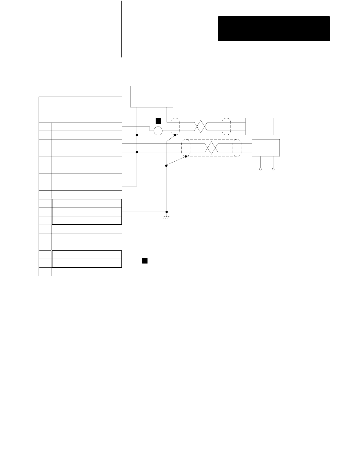
Figure 2.6
Connections to Input Devices
Chapter 2
Aseembly and Installation
PID Module
TERMINAL IDENTIFICATION
CAT. NO. 1771-PDC
TERMINAL FUNCTION
INPUT 1 (+LEAD)
18
INPUT 1 (-LEAD)
17
INPUT 2 (+LEAD)
16
INPUT 2 (-LEAD)
15
TIEBACK INPUT 1
14
TIEBACK INPUT 2
13
ANALOG OUTPUT 1
12
MODULE COMMON
11
ANALOG OUTPUT 2
10
+ 15V DC
9
+
15V DC COMMON
8
-
- 15V DC
7
MANUAL MODE 1
6
MANUAL MODE 2
5
4
MANUAL REQUEST
OPT. +5V DC COMMON
3
2
OPTIONAL +5V DC
NOT USED
1
POWER
SUPPLY
-
1
+
1
R
If used connect a recorder or other monitoring instrument in series with
the transmitter on the transmitter return lead.
(+)
(-)
(+)
(-)
2-Wire
Transmitter
+4 to 20mA
4-Wire
Transmitter
+1 to 5V DC
-
+
V
11102
215
Page 29
Chapter 2
Assembly and Installation
PID Module
TERMINAL IDENTIFICATION
CAT. NO. 1771-PDC
TERMINAL FUNCTION
INPUT 1 (+LEAD)
18
INPUT 1 (-LEAD)
17
INPUT 2 (+LEAD)
16
INPUT 2 (-LEAD)
15
TIEBACK INPUT 1
14
TIEBACK INPUT 2
13
ANALOG OUTPUT 1
12
MODULE COMMON
11
ANALOG OUTPUT 2
10
+ 15V DC
9
+
15V DC COMMON
8
-
- 15V DC
7
MANUAL MODE 1
6
MANUAL MODE 2
5
4
MANUAL REQUEST
OPT. +5V DC COMMON
3
2
OPTIONAL +5V DC
NOT USED
1
Figure 2.7
Connections
1
2
to MODULE COMMON terminal 11.
to Output Actuators
1
2
If tieback is not used to monitor a voltage output, do not make this
connection.
if tieback is not used to monitor a current output, connect the return lead
(+)
(-)
(+)
(-)
Actuator
+1 to +5V DC
+4 to +20mA
Actuator
11103
216
Page 30
PID Module
TERMINAL IDENTIFICATION
CAT. NO. 1771-PDC
TERMINAL FUNCTION
INPUT 1 (+LEAD)
18
INPUT 1 (-LEAD)
17
INPUT 2 (+LEAD)
16
INPUT 2 (-LEAD)
15
TIEBACK INPUT 1
14
TIEBACK INPUT 2
13
ANALOG OUTPUT 1
12
MODULE COMMON
11
ANALOG OUTPUT 2
10
+ 15V DC
9
+
15V DC COMMON
8
-
- 15V DC
7
MANUAL MODE 1
6
MANUAL MODE 2
5
4
MANUAL REQUEST
OPT. +5V DC COMMON
3
2
OPTIONAL +5V DC
NOT USED
1
Figure 2.8
Mode Connections to Manual Control Station
Control
Chapter 2
Aseembly and Installation
General
Manual Control
Station
Auto/Manual
Switch
Manual
Request
Input
Manual Control Station Interface
11104
The PID module is designed for use with commercially available manual
control stations, one per loop. The station is connected between the
analog output and the controlled element of the process. The station
provides manual override control and automatic backup to the PID
module. Manual control stations can be used for start-ups, on-line process
adjustments, and routine maintenance. The station can be used in either
of two ways, manual override control or module back-up.
Manual Override Control
An operator can override automatic control by switching to manual
control and adjusting the output at the manual control station. When the
manual control station is switched to manual mode, a connection is closed
between the MANUAL MODE terminal (referenced to +15V dc) and the
MODULE COMMON terminal on the PID module (Figure 2.8). This
217
Page 31

Chapter 2
Assembly and Installation
allows the PID output to be switched open at the manual control station
and a manually controlled output to be switched into the system.
When in manual mode, care should be taken not to return to automatic
control when the output is below +1V dc or +4mA. If attempted, an
output surge could occur. The PID module performs a bumpless transfer
when the tieback input is tracking a signal at or above the minimum level
of +1V dc or +4mA. Also, the PID module’s operating mode must
include integral control and the manual mode status line must be closed at
the manual control station. The module monitors tieback inputs only
when you enable manual control.
Module Backup
The manual control station can be used to automatically backup the PID
module in the event of module failure. A module failure would
de-energize the PID module’s contact output and generate a manual
request to the manual control station causing control to be transferred in
the following manner.
The contact output (Figure 2.9) is a normally closed contact. When the
PID module is in normal operation, the contact will be held open. A
manual request is generated by contact closure. The contact will close
and remain closed in the event of module failure or loss of +
15V dc
analog power. Contact closure internally switches the signal at terminal 4
MANUAL REQUEST to terminal 11 MODULE COMMON. There is
only one contact output. If two manual control stations are used, both will
be switched simultaneously.
If a manual request is generated by program logic, contact closure is a
one-shot 50 millesecond closure. The closure can be used to activate an
alarm device by connecting a latching relay to terminal 4 MANUAL
REQUEST and terminal 11 MODULE COMMON on the PID module.
Once the PID module relinquishes control to the manual control station,
the plant operator must physically reset the operation to automatic mode
using a switch on the manual control station.
When control is returned from manual to automatic at the manual control
station, the PID module performs a bumpless transfer if the tieback analog
input is used to track the output from the manual control station and the
PID module’s operating mode includes integral control.
218
Page 32
Figure 2.9
Connections to the Field Wiring Arm
Internal
Chapter 2
Aseembly and Installation
1771 - PID Module
Ω
250
2
E11 E12
Standard
1
Compliance
Additional
250
Internal Connections
Input 1 (+ Lead)
Input 2 (+ Lead)
Tieback Input 1
Tieback Input 2
Ω
Analog Output 1
Module Common
Analog Output 2
+15V DC
+
-
-15V DC
15V DC Common
1771 - WF
Wiring Arm
External
Connections
18
17
16
15
14
13
12
11
10
9
8
7
6
5
4
3
2
1
Station 1
Station 2
Manual
Request
Station 1
Manual
Request
Station 2
3
Contact Output
(normally closed)
E22 E21
30V peak
1/4 AMP Max.
Max. 3VA
OptoIso
NOTE: Optional +5V DC power supply wiring is not shown.
1
Standard compliance selects module common as 15V DC Common (500 max for current outputs.)
Additional compliance selects module common as -15V DC Common (1250 max for current outputs.)
2
Programming plugs inserted for current mode.
Programming pl ugs inserted for standard compliance.
3
Input Power Supply Requirements
The source of power for the input loop when the input is configured for
current mode can be either the analog +
supply. The choice depends on the selected output compliance and the
number of devices in the loop.
Manual Mode 1
Manual Mode 2
Manual Request
+
-
Ω
Ω
11105
15V dc supply or a separate
219
Page 33

Chapter 2
Assembly and Installation
+15V dc Analog Supply
When both the module outputs and tieback inputs (if used) are configured
in current mode, additional compliance can be selected. As such, module
common is internally connected to -15V dc. The +
15V dc analog power
supply can provide a 30 V dc source to the input current loop by
jumpering the +15V Dc terminal of the PID module to the positive lead of
the current transmitter (Figure 2.10). The potential of 30 V dc is enough
to provide the required voltage drops for the transmitter, PID module, and
manual control station.
220
Page 34

Figure 2.10
Mode Input Using External +
Current
Chapter 2
Aseembly and Installation
15V dc Supply
PID Module
1771-PD
TERMINAL IDENTIFICATION
CAT. NO. 1771-PDC
TERMINAL FUNCTION
INPUT 1 (+LEAD)
18
INPUT 1 (-LEAD)
17
INPUT 2 (+LEAD)
16
INPUT 2 (-LEAD)
15
14
TIEBACK INPUT 1
13
TIEBACK INPUT 2
ANALOG OUTPUT 1
12
MODULE COMMON
11
ANALOG OUTPUT 2
10
9
+ 15V DC
+
8
15V DC COMMON
-
- 15V DC
7
MANUAL MODE 1
6
MANUAL MODE 2
5
4
MANUAL REQUEST
OPT. +5V DC COMMON
3
OPTIONAL +5V DC
2
1
NOT USED
Two-Wire
Transmitter
+4 to +20mA
(+)
(-)
R
General
Manual Control
Station
PV
Input
R
Recorder or indicating instrument if used
10997
Separate Supply
If additional compliance is not selected (as when one of the module
outputs is configured in voltage mode), a separate DC power supply must
be used to power the input current loop.
Power Supply Voltage
When selecting the power supply to operate the input current loop, the
required voltage must be equal to the voltage drop across all impedances
at the maximum current of 20mA. Current transmitters typically require a
voltage drop of 18V dc or more. The process variable input impedance of
the PID module (250 ohms), manual control station (100 ohms), recording
221
Page 35

Chapter 2
Assembly and Installation
or indicating instrument if used (typically 250 ohms) must be considered
when calculating the voltage drop in the loop.
For example, the required voltage for an input loop that contained the PID
module, manual control station, and current transmitter that requires at
least 18V dc would be 18V +2 (250 ohms) (.020 amps)= 18V +10V =
28V dc. Up to 2 V dc could be allowed for voltage drops in the cables
when using a 30 V dc source such as the +
15V dc analog power supply
with the module output configured for current operation and additional
compliance.
If the input loop were to contain a chart recorder and an indicating
instrument (250 ohms each) in addition to the basic loop in the previous
example, the power supply would have to provide a least 38V dc plus an
amount equal to the voltage drop of the cables. A separate power supply
would have to be used.
Installation Practices
Power Supply Current
The +
15V dc analog power supply must provide 100mA to the PID
module’s analog circuits. This includes 20mA that the module provides to
each output current loop. If the +
15V dc supply is providing 20mA to
each input current loop, a 2-loop control system will require 140mA. This
is within the specification for the Allen-Bradley 1770-P1 power supply
rated at 150mA at +
15V dc.
To minimize the effects of electromagnetic interference (EMI), group
analog modules together in the I/O chassis whenever possible. Avoid
placing PID modules close to AC modules or high voltage DC modules.
It is important to use shielded cable when wiring analog signals. Belden
8761 or equivalent cable has an insulated twisted pair of conductors
covered by a foil shield. To reduce the effect of EMI induced noise along
the cable, the shield must be properly grounded at one end, only. The
recommended grounding point for each cable is identified in the wiring
diagram (Figure 2.5-Figure 2.8 and Figure 2.10). One end of the shield
should be cut short and taped to insulate it from any electrical contact.
The other end should be tied to a common point at earth ground.
222
Optional Instrument Grounding Bus
An alternate grounding system can be used to separate analog signal
ground from the grounding of equipment such as motor starters and are
Page 36

Chapter 2
Aseembly and Installation
welders which generate high electrical noise. Equipment grounding can
carry electrical noise when ground loops exists.
The alternate grounding method is for instruments, only. A instrument
ground bus is located inside the enclosure containing the I/O chassis,
manual control station, and PC processor. The instrument bus is
electrically isolated from the I/O chassis and enclosure. The bus is
connected to earth ground by a direct path, independent of other
equipment ground connections.
When using instrument grounding, the only change to the connection
drawings (Figure 2.5 through Figure 2.8 and Figure 2.10) is that the
chassis ground symbol would be redefined as instrument ground. All
cable shields and the +
15V dc COMMON terminal of the PID module
would be connected to the instrument ground bus.
Chassis Considerations
When multiple PID modules are placed in the same chassis, the +
15V dc
commons and +5V dc commons, if used, should be connected to the
ground bus at one point. Do not daisy-chain the commons.
The PID dual-slot module must be placed with single module group when
placed in a I/O chassis. Up to eight PID modules can be placed in a single
128 I/O chassis. Up to four of the PID modules can be powered from the
+5V I/O chassis power supply. The remaining PID modules, if installed,
must be powered by a separate +5V dc supply through the field wiring
arm +5V dc and 5V dc COMMON terminals. Be sure that the total
current requirement for all modules in the I/O chassis using the I/Ochassis
power supply does not exceed the rating of the I/O chassis and the I/O
chassis power supply.
Avoid placing the PID module close to AC I/O modules or high voltage
DC I/O modules. It cannot be inserted in the left-most slot reserved for the
processor module in a single I/O chassis system or for the I/O adapter
module in a multi-chassis system.
Set switch 1 of the I/O chassis last state switch assembly to the off
position to allow PID module operation in soft fault mode. Refer to
section titled Loop Control Word B for additional information on soft
fault mode selection.
Other intelligent I/O modules can operate without interference in the same
I/O chassis with PID modules.
223
Page 37

Chapter 2
Assembly and Installation
Internal Fusing
The PID module has internal pico fuses to protect circuitry from surges in
the optional +5V dc supply., A blown fuse condition is indicated when
none of the front panel LED indicators turn on after you turn on this
supply. If the LEDs do not turn on, check programming plugs E23 and
E24. These plugs allow you to select the source of +5V dc from the
backplane or from an external supply. Incorrect positioning of these plugs
can prevent the LEDs from turning on even when pico fuses are OK.
Check that E23 and E24 are in the correct position for using the external
+5V dc supply (Table 2.D and Figure 2.3).
If the fuses are blown, we recommend that you return the module for
factory repair through your nearest field service or sales office.
Unauthorized repair of these fuses could result in damage to other circuit
components and void your warrantee.
Precautions
Take the following precautions to avoid blowing these fuses:
Be sure that the optional +5V dc supply is connected correctly to field
wiring arm terminals (Figure 2.4).
Be sure that the optional +5V dc supply meets specifications
(Table 2.G), especially for surge voltage at turn on.
Supply +5V dc to each PID module using one or more optional external
power supplies.
Place an on/off switch in the +5V dc lead to each PID module. This
allows you to remove power and replace a PID module without turning
off power to other PID modules in the chassis.
Remove power from the PID Module’s field wiring arm before
connecting or disconnecting the arm.
Recommendations for Installing
or Removing Modules
224
We make the following recommendations for removing one of several
PID modules from an I/O chassis.
WARNING: Remove power from a field wiring arm before
connecting or disconnecting it. Turn off power to the I/O
chassis before inserting or removing any of its modules. Failure
to observe this warning can result in damage to module circuitry
and/or unpredictable operation of other modules in the chassis
with possible damage to equipment and/or injury to personnel.
Page 38

Chapter 2
Aseembly and Installation
Place PID modules in one or more chassis containing only PID
modules.
Supply +5V dc to each PIC module using one or more optional external
power supplies.
Place an on/off switch in the +5V dc lead to each PID module. This
allows you to remove power and replace a PID module without turning
off power to other PID modules in the chassis.
Removal of a Faulted PID Module
You can replace a faulted PID module in an I/O chassis using the
following procedure if each PID module is supplied with +5V dc from a
separate power supply or from a common supply with a switch in each
+5V dc lead.
1. Select the soft fault mode that allows PID modules to continue
operation when they lose communication with the PC processor. Do
this by means of your ladder program.
2. Turn off power to the I/O chassis. Block transfers cease but PID
modules continue to operate.
3. Turn off the +5V and +
15V dc power to the faulted module.
4. Replace the faulted PID module.
5. Turn on power to the module and I/O chassis.
6. Restore the original soft fault mode to the PID modules.
If there are other modules and/or other PID modules without an external
+5V dc supply, they cease to operate when you turn off power to the
chassis. After restoring power, you must download PID control
parameters to PID modules through a load/enter sequence.
Keying
PID modules (rev C or later) have the option for you to select how outputs
respond when +5V dc is removed from the module. You select either
maximum or minimum, output using programming plus (refer to titled
Programming Plug Selection).
The backplane connector should be keyed to accept only this module after
its position in the I/O chassis has been determined.
225
Page 39

Chapter 2
Assembly and Installation
Plastic keying bands shipped with the I/O chassis should be used. The
position of the keying bands on the upper backplane connector must
correspond to the mating slots on the module connector.
Refer to Figure 2.11. Using needle-nose pliers, place the keying bands on
the backplane connector between these numbers:
Slot 0 (left)
8 and 10
18 and 20
slot 1 (right)
2 and 4
28 and 30
The position of the keying bands can be changed if subsequent system
design requires the module to be moved to a different location.
226
Page 40

Figure 2.11
Diagram
Keying
Chapter 2
Aseembly and Installation
Single Module Group
0PID Module 1
Upper Backplane Connectors
Power Supply Specifications
Keying
Bands
2
4
6
8
10
12
14
16
18
20
22
24
26
28
30
32
34
36
Left
Connector
2
4
6
8
10
12
14
16
18
20
22
24
26
28
30
32
34
36
Right
Connector
11106
Isolation must be maintained between the analog and digital circuits of the
PID module to minimize electrical noise interference. Therefore, separate
power supplies must be used for the analog +
15V dc supply and for the
digital +5V dc supply.
The requirements for the customer +
15V dc power supply and for the
optional +5V dc power supply are listed in Table 2.E and Table 2.F,
respectively.
227
Page 41

Chapter 2
Assembly and Installation
Table 2.E
Customer
Output Current
Output V
Regulation (type)
Line Regulation (for 10V AC input change)
Load Regulation (no load to full load)
Ripple 10mVpp 10mVpp
Overvoltage Protection
Current Limit (percent of full load)
[1] The module is not protected from overvoltages from the customer power supply
Table 2.F
+5V dc Power Supply (Optional) Requirements
+
15V dc Power Supply Requirements
Specifications
oltage T
olerance 1% 1%
[1]
+15 V
100mA 100mA
Series Series
+0.2% +0.2%
+1.0% +1.0%
+18V dc 18V dc
125% 125%
olts
15 V
.
olts
Specifications +5Volts
V
oltage (at wiring arm)
Current
V
oltage Regulation
Rise T
ime (to 4.75V dc) Less than 10msec
5.05V dc
1.2A per PID module
Sum of all deviations due to line,
load, and ripple should not exceed
+
0.15V dc
228
Page 42

Chapter 2
Aseembly and Installation
Module Specifications
V
Process
Number 12binary
Configuration
Range (userselectable)
Digital Resolution
ariable Inputs
process variable input 1
process variable input 2
Differential
+4 to +20mA
+1 to +5V dc
12bit binary
, 1 part in 4095
The PID module specifications are listed in Table 2.G.
Table 2.G
Specifications
Digital Resolution Maximum Current
Accuracy
+
0.1% of range at 250C3VA
Input Impedance
250 ohms (current)
4.7 megohms (voltage)
Maximum Allowable Input
+
30mA (current)
25V rms (voltage) Backplane or External (Digital Circuits)
T
emperature Coefficient
, 1 part in 4095
250mA
Maximum Power
Digital Inputs (from manual
manual control station)
T
wo independent inputs for moni
toring
Power Requirements
1.2A at +5V dc
Accuracy +
+
0.1% of range at 250C
Input Impedance
250 ohms (current) analog output 1
10 megohms (voltage)
Common Mode Rejection Ratio
70dB DC
Common Mode V
+
common
Common Mode Input Resistance referenced to power supply Relative Humidity Rating
2.5 megohms
Input Frequency Respnse
3dB at 1kHz
Maximum Allowable Input
oltage Range
200V with respect to module +4 to +20mA
Number
Configuration
Range (userselectable)
50 ppm/0C
Analog Outputs 100mA A
analog output 2 100msec, typical
Single ended
(With output common internally
common
the output will drive up to a 500 ohm
load over the full current range.
+1 to +5V dc
External (Analog Circuits)
100mA at 15V dc
Loop Update T
Ambient T
Operation 00C to 600C (320F to
1400F
Storage 400C to 850C (400F to
1850F)
5% to 95% (without condensation)
Electrical Isolation
[1]
1500V rms (transient
(Isolation is achieved by
T +15V dc
ime
emperature Ratings
+
30mA (current)
(500 ohms minimum load resistance
optoelectronic coupling between I/O
229
Page 43

Chapter 2
Assembly and Installation
dc (voltage) 10mA maximum load current.)
125V
T
emperature Coeffeicient
+
50 ppm/0C
T
ieback Inputs
Number +
tieback input 1
tieback input 2
Configuration
Single ended
Range (userselectable)
+4 to +20mA
+1 to +5V dc
Digital Resolution
Accuracy
T
emperature Coefficient
Number
Peak V
oltage
analog circuit and control logic)
Keying
12bit binary
0.1% of range at 250C
+
50 ppm/0C
one normally closed contact,held extended from 500ohms (standard compli
open
30V
, 1 part in 4095
Contact Output
Left connector (slot 0) between 8
and 10, 18 and 20
Right connector (slot 1) between 2
and 4, 28 and 30
[1]
If all analog outputs and tieback inputs
used are selected to current mode, the
compliance of the analog outpus can be
ance to 1250 ohms(additional compliance).
This is achieved by internally referencing the
outputs to 15V dc.
230
Page 44

Programming
Chapter
3
General
Before starting to program the PID module, read this entire chapter
thoroughly. Be sure that the programming plug functions have been
selected as described in section titled Programming Plug Selection.
The PID module can be programmed in four general steps:
1. Choose the PID module features required for the application. These
are listed in section titled Capabilities (chapter 1) and are presented
in the algorithm flow chart (Figure 3.15).
2. Identify the control bits and loop storage words which must be
programmed to implement the features. These are defined in section
titled Word and Bit Definitions. Record the values of the storage
words and the logic state of the control bits on the worksheets found
in appendix A.
3. Write the ladder diagram program and assign data table addresses to
the data blocks used to store loop values. The examples presented in
appendix B or C should be used as guides.
4. Using a industrial terminal, enter the program into memory and the
block data into the data table. Refer to the worksheets on which the
values of the loop storage words have been recorded. Set the
appropriate control bits.
Sections listed below provide information for selecting PID module
features and programming the module.
Section titled Operational Overview provides an overview of the
programming concepts which are used to program and monitor the PID
module.
Section titled Word and Bit Definitions defines the words and bits
which can be used to program the module.
Section titled Algorithm Flow Chart contains the algorithm flow chart
and explains it use.
Section titled Block Transfer Programming explains how the module is
programmed using block transfer instructions.
31
Page 45

Chapter 3
Programming
Section titled Programming Consideration explains the application of
block transfer instructions.
Section titled Expanded Features describes the expanded features of the
PID module and how they can be applied.
Additionally, four appendices contain helpful programming information:
Appendix A contains the worksheets which are used to record data that
is entered into the PC processor and transferred to the PID module.
Appendix B describes a program that performs continuous block
transfers to the PID module. This program may be used when
continuous parameter adjustment or continuous reporting of module
status is required for a critical application.
Appendix C describes a program that performs periodic block transfers
to the PID module. This program may be used when less frequent
parameter adjustment is required.
Appendix D contains summary word and bit tables and a word/bit
reference.
Operational Overview
The PID module is a closed loop process controller with proportional,
integral, and derivative control action. Control algorithm features are user
determined and loaded in the PID module by block transfer from the PC
processor. The PID module is equipped to control up to two process
control loops using its internal microprocessor. Because the features of
the two loops are similar, the description will be general to both loops
except where otherwise stated. Each loop is individually configured with
its own parameter values.
PID Algorithm
The PID module contains features which are user-selected to perform the
desired control. Figure 3.1 is a simplified diagram of the PID module
features. Basically, the PID module reads the process variable, compares
it to the set point, and adjusts the analog output to make the process
variable equal the set point. The process variable PV is the analog input
from the process. The setpoint SP is the equilibrium value of the process,
and the analog output is the control variable to the process. The
difference between the set point and the process variable is the error
signal, E=SP-PV.
32
The PID module can perform a combination of proportional, integral and
derivative control. Integral control is also known as reset action.
Derivative control is also known as rate action. The PID module can
perform relatively simple or very complex control based on selected
Page 46

Chapter 3
Programming
features. The full algorithm flow chart is presented in section titled
Algorithm Flow Chart.
The PID module (rev C or later) uses the ISA algorithm (P, I and D
dependent gains) or the Allen-Bradley algorithm (P, I and D independent
gains). Refer to appendix E for algorithm comparison and selection.
Earlier revision modules use only the Allen-Bradley algorithm.
Figure 3.1
Simplified
PID Algorithm
Feedforward Input
Process
Variable
A/D
Hardware
Analog
Input
/
SP
+
-
/
Digital
Filter
PV
S
Error=SPPV
P
I
D
SS
Lead
Lag
BIAS
V
PID
V
(FFV)
Control Variable
D/A
Hardware
Analog
Output
11093
Block Transfer Data Blocks
Data block files are areas of the PC processor data table used to store loop
control words and loop values. The features of the module are selected by
setting word and bit values in data block files. The data block files are
transferred to the PID module by block transfer instructions.
Three write block transfers are required to load the PID module with data
from three data table block files. The dynamic block DB contains values
which are subject to change for both loops. The loop 1 block LP1 and
loop 2 block LP2 contain loop constants which seldom change.
33
Page 47

Chapter 3
Programming
The status block SB is a read block transfer file used to report the current
status of the PID module and any alarm condition detected by the module.
The transfer of the status block is also used to prompt the next write block
transfer.
Figure 3.2 illustrates the multiple block concept.
Figure 3.2
Multiple
Block Concept
PCProcessor
DataTable
Dynamic
Block
Loop1
Constants
Block
Loop2
Constants
Block
Status
Block
PIDModule
WriteBlock
Transfer
WriteBlock
Transfer
WriteBlock
Transfer
ReadBlock
Transfer
11094
34
PC Processor Memory Requirements
The PID module requires multiple files in the C processor data table to
store the different blocks of data. Storage requirements are determined by
the features selected. The module can be configured for one or two loops
with either standard or expanded features. There are four different
memory requirements for storing block of data (Figure 3.3).
User program memory requirements will vary depending on the
application. Examples are shown in appendicies B and C.
Page 48

Chapter 3
Programming
Figure 3.3
File Memory Requirements
Block
1 Standard Loop 1 Expanded Loop 2 Standard Loops 2 Expanded Loops
Dynamic
Block
10 Words
Loop 1 Constants
Block
12 Words
Status Block
11 Words
Dynamic
Block
10 Words
Loop 1
Constants
Block
19 Words
Status Block
11 Words
Dynamic
Block
17 Words
Loop 1 Constants
Block
12 Words
Loop 2 Constants
Block
12 Words
Status
Block
18 Words
Dynamic
Block
17 Words
Loop 1
Constants
Block
19 Words
Loop 2
Constants
Block
19 Words
Status
Block
18 Words
Load/Enter Sequence
The load/enter sequence is used when all PID control parameters
(dynamic block and loop block data) are transferred from the PC
processor to the PID module. The load/enter sequence is required at
power-up and whenever it is necessary to change any of the loop
constants in LP1 or LP2 or selected control bits in the master control
word. (After a load/enter sequence has been completed, dynamic block
data can be changed at any time by a write block transfer). Changes to
loop constants require a load/enter sequence as a safety consideration to
prevent inadvertent changes which could adversely affect the system.
11095
35
Page 49

Chapter 3
Programming
The PID module prompts the sequencing of block transfers. The write
block transfer instruction in the user program contains the data table
address of the first word of the block file to be transferred. By
manipulating this address, different data block files can be transferred
with the same write block transfer instruction.
There are three control bits which are associated with the handshaking of
the load/enter sequence.
The load bit is set in the dynamic block to allow the PID module to
accept dynamic block data and to load loop 1 and loop 2 constants into
the module’s buffer.
The ready bit is returned in the status block to indicate that the write
block transfers were acceptable and that the module is able to process
the information.
The enter bit is set to activate the information in the module’s buffer
and to start control based on the new parameters transferred during the
load/enter sequence.
An overview of the load/enter sequence is presented in Figure 3.4.
Additional information can be found in sections titled Power-up
Load/Enter Sequence and Load/Enter Sequence.
36
Page 50

Chapter 3
Programming
Command
Load
Bit
1
1
1
Enter
Bit
0
0
0
Status
Ready
Bit
0
0
0
P
R
O
C
E
S
S
O
R
Figure 3.4
Load/Enter
Sequence
Block Transfers
read
write
1st
SB
2nd
DB
3rd
SB
4th
LP1
5th
SB
6th
LP2
Description
1st The processor reads the status block to start
the sequence.
2nd
The processor writes the dynamic block to the
PID module (load bit set) to transfer dynamic
block data.
3rd The processor reads the status block to confirm
dynamic block data and to address the next
block transfer.
P
4th The processor writes loop constants to the module
I
D
M
O
D
U
L
E
to set the features for loop 1.
5th The processor reads the status block to confirm
loop 1 constants andd to address the next
block transfer.
6th
The processor writes loop constants to the module
to set the features for loop 2.
1
0
0
1
0
0
SB = Status Block, DB = Dynamic Block, LP1 and LP2 = Loop 1 and Loop 2 Parameter Blocks
7th
SB
8th
DB
9th
SB
DB
SB
7th The processor reads the status block to confirm the
data for the entire sequence (readdy bit set) and to
address the next block transfer.
8th The processor writes the dynamic block to the
module to start PID control (enter bit set).
9th
The processor reads the status block to confirm
that the module has been programmed and no
errors were detected.
Toggle sequence or periodic block transfers.
11107
37
Page 51

Chapter 3
Programming
Word and Bit Definitions
This section defines the words and bits of the three write blocks and the
single read block. For ease of reference, the following word and bit
notation is used throughout the manual:
A PID module word is abbreviated as Wxx.
Example: Word number 12 = W12.
A PID module bit is abbreviated as Bxx.
Example: Bit number 07 = B07.
The word and bit abbreviations can be used together.
Example: Word number 12, Bit number 07 = W12 B07.
Other notations which will be used are (LE) and (XF). The symbol (LE)
is used to designate the four bits in the master control word which require
a load/enter sequence to occur before the PID module will accept a
change to them. The symbol (XF) is used to designate words or bits
which are used to select the Expanded Features of a loop.
For ease of reference, the parameter words required to program the
module are numbered consecutively in the following sections.
38
Section titled Dynamic Block: Words W01-W17.
Section titled Loop Constants Block: W18-W36 for loop 1,
W38-W56 for loop 2.
Section titled Status Block: W57-W74.
Dynamic Block: Words W01W17
The dynamic block is a write block transfer file of up to 17 words. It is
used to establish the features of the PID module, to program the most
frequently changing (dynamic) parameters of loop 1 and loop 2, and to
load information required by the PID module for controlling the block
transfer sequences.
If loop 1 is selected, only words W01 must be programmed. If both loops
are selected, then the entire 17 word block must be programmed.
The 17 words of the dynamic block are defined in the paragraphs that
follow. Table 3.A lists the dynamic block words. All the words of the
Page 52

Chapter 3
Programming
dynamic block, loop blocks and status block are listed in Table 3.J,
Figure 3.13 and Figure 3.14 found at the end of section title Word and Bit
Definitions.
Table 3.A
Dynamic
Block W
ords
W01
W02
W03
W04
W05
W06
W07
W08
W09
W10
W11
W12
W13
W14
W15
W16
W17
Word
Master Control W
Control W
Dynamic Block Start Address
Loop 1 Block Start Address
Set Analog Output 1
Set Point 1
Proportional Gain 1
Bias 1
Set Process Variable 1
Set Feedforward Input 1
Loop 2 Block Start Address
Set Analog Output 2
Set Point 2
Proportional Gain 2
Bias 2
Set Process Variable 2
Set Feedforward Input 2
ord
Title Abbreviation
ord
SET OUT 1
SP1
K
p
BIAS 1
SET PV1
SET FFI1
SET OUT 2
SP2
K
p
BIAS 2
SET PV2
SET FFI2
1
2
W01 Master Control Word. This word initiates all activities in the PID
module from power-up. This word programs the module configuration,
controls the initiation of the block transfer sequences, and can control the
setting of the analog outputs and the contact output. Bits 17 through 00
are defined below and summarized in Figure 3.5.
W01 B17, B16 Block Identifiers. Both bits must be set to 1 to
identify this block as the dynamic block.
W01 B15 Loop Select. [LE] Reset to 0 selects both loop 1 and loop
2. Set to 1 selects loop 1 only. When loop 1 and loop 2 are selected,
all words in the dynamic block are used and both loop blocks must
be programmed. When loop 1 is selected, only words W01 through
W10 of the dynamic block are used and the loop 1 block must be
programmed.
W01 B14 Standard/Expanded Features. [XF], [LE] Reset to 0
selects standard loop features. When the stand loop is selected, loop
1 words W30 through W36 and loop 2 words W50 through W56 are
NOT used by the module. Set to 1 selects expanded loop features
39
Page 53

Chapter 3
Programming
such as feedforward, scaling, lead/lag, and all the words in the loop
block must have a value. The value of unused expanded feature
words must be zero.
W01 B13 Calibration. Reset to 0 selects normal operation. Set to 1
only for calibrating the module. This bit is examined only at
power-up, and is used with W02 B17 and B16.
310
Page 54

Figure 3.5
Control W
Master
Chapter 3
Programming
ord W01
W01 B17 Must be set to 1
W01 B16 Must be set to 1
W01
W01 B15 1=Loop 1 only
0=Both Loop 1 and Loop 2
W01 B14 1=Expanded loop features
0=Standard loop features
W01 B13 1=Calibration
0=Normal Operation
W01 B12 1=Binary format for words W05, W09, W10,
W12, W16, W17, W63, W64, W66, W70,
W71, and W73
0=BCD format
W01 B11 1=Binary format for the set point W06 (W13)
0=BCD
W01 B10 1=Soft Fault Reset
0=Remain in Soft Fault
17 16 15 14 13 12 11 10 07 06 05 04 03 02 01 00
SP
BCD
SOFT
FAULT
RESET
EXPANDED
1
1
0
LOOP 1
1
2 LOOPS
STANDARD
CALIB BINARY
BCD
BINARY
DIAG
LOOP
TIME
LOAD
VERIFY
CODE
00
ENTER
SET
OUTPUT 2
W01 B07 1=Report diagnostics in W60
0=Report loop time in W60
SET
OUTPUT 1
MANUAL
REQUEST
1
0
W01 B06 1=Initiates load/enter sequence
0=Sequence not initiated
W01 B05 Must be set to 0
W01 B04 Must be set to 0
W01 B03 1=Completes the load/enter sequence
0=Loop constants remain in buffer
W01 B02 1=Set Analog Output 2 (W12)
0=Use algorithm output
W01 B01 1=Set Analog Output 1 (W05)
0=Use algorithm output
W01 B00 1=Contact closure oneshot
0=Off; resets oneshot
11108
311
Page 55

Chapter 3
Programming
W01 B12 Binary/BCD Format. [LE] Reset to 0 selects the 4-digit
BCD (4095 maximum) format. Set to 1 selects the 12-bit are listed
in Table 3.B.
Table 3.B
Binary/BCD
Format W
ords
Word
W05
W09
W10
W12
W16
W17
Set Analog Output 1
Set Process V
Set Feedforward Input 1
Set Analog Output 2
Set Process V
Set Feedforward Input 2
Title Word Title
ariable 1
ariable 2
W63
W64
W66
W70
W71
W73
Read Loop 1 Output
Read Analog Input 1
Read T
ieback Input 1
Read Loop 2 Output
Read Analog Input 2
Read T
ieback Input 2
W01 B11 Set Point Format. [LE] Reset to 0 selects 4-digit BCD
(4095 maximum) format for set point 1 in word W06 and set point 2
in word W13. Set to 1 selects the 12-bit binary (4095 maximum)
format. If scaling has been selected by B16 = 1 in word W30 for
loop 1 or in W50 for loop 2, the 4-digit BCD value has the data
format of 9999.
W01 B10 Soft Fault Reset. Reset to zero holds the module in soft
fault mode until this bit is set to 1. Set to 1 allows recovery from the
soft fault mode after the fault is corrected. Soft fault mode is
signified by W58 B10 = 1 and is indicated by the flashing
STAND-ALONE yellow LED on the PID module. The soft fault
mode of operation is selected by bits B15, B14, B13 in word W19
for loop 1 and W39 for loop 2.
312
W01 B07 Loop Time/Diagnostic. Reset to 0, causes word W60 to
report loop update time. Set to 1 causes word W60 to report error
codes. The upper byte of word W 60 reports dynamic block error
codes. The lower byte reports error codes and loop 1 and loop 2
blocks.
W01 B06 Load. Reset to 0 inhibits the load/enter sequence. Set to 1
initiates the load/enter sequence.
When the load bit is set, the loop constants are loaded into the
module’s buffer. They are not used until the enter bit is set at the
completion of a load/enter sequence. The same applies to the four
bits in the master control word W01 B15, B14, B12, B11 designed
Page 56

Chapter 3
Programming
by (LE). These bits are protected from accidental change because
they control the number of PID loops, standard or expanded loop
features and binary or BCD data format. These bits can be changed
in the same manner that loop constants are changed, only by a
load/enter sequence. The remaining bits in the master control word
and the remaining dynamic block words can be changed at any time
by a write block transfer. See sections titled Power-Up Load/Enter
Sequence and Load/Enter Sequences.
W01 B05, B04 Verify. Both bits must be set to 0 for normal
operation.
W01 B03 Enter. Used with load bit W01 B06 to complete a
load/enter sequence. when 0, the data previously loaded remains in
the module’s buffer. Set to 1 the buffered data is moved from the
buffer into the module’s active area and the sequence is completed.
The buffered data includes all loop constants and the four (LE) bits
in the master control word W01 B15, B14, B12, B11. See sections
titled Power-Up Load/Enter Sequence and Load/Enter Sequence.
W01 B02 Set Output 2. Reset to 0 selects the analog output value
determined by the module’s PID algorithm. Set to 1 selects the
analog output as the value stored in word W12, Set OUT2,
downloaded from the PC processor. When reset to 0, the analog
output value is adjusted automatically from the SET Out value to the
value determined by the PID algorithm, a bumpless transfer.
W01 B01 Set Output 1. Reset to 0 selects the analog output value
as determined by the module’s PID algorithm. Set to 1 selects the
analog output as the value stored in word W05, SET OUT1,
downloaded from the PC processor. When reset to 0, the analog
output value is adjusted automatically from the SET OUT value to
the value determined by the PID algorithm, a bumpless transfer.
W01 B00 Set Manual Request. Reset to 0 the PID module inhibits
contact closure. Set to 1 generates a contact closure for 50msec. To
repeat this one-shot closure, it is necessary to first reset this bit to 0
and then set it to 1 again.
W02 Control Word. Use this word to select ISA or A-B values for the
PID algorithm, or to select module calibration.
W02 B17, B16 Calibration. Refer to chapter 5.
313
Page 57

Chapter 3
Programming
W02 B00 PID Algorithm. Reset to 0 the PID module uses A-B gain
values. Set to 1 the PID module uses ISA values.
W03 Dynamic Block Start Address. This word contains the data table
address of the first word in the file associated with the dynamic block.
The address is required by the PID module to prompt the transfer of the
dynamic block.
W04 Loop 1 Block Start Address. This word contains the data table
address of the first word in the file associated with the loop 1 block. The
address is required by the PID module to prompt the transfer of loop 1
constants.
W05 Set analog Output 1, SET OUT1. The value stored in this word
becomes the analog output when W01 B01 = 1.
Normally, the PID module outputs the PID algorithm value when W01
B-1 = 0. Data format is 4-digit BCD or 12-bit binary. Format is
determined by W01 B12. Range is 0000 to 4095.
W06 Set Point 1, SP1. This word contains the set point value for loop 1.
Data format is 4-digit BCD or 12 bit binary as selected by W01 B11. The
unscaled range is 0000 to 4095.
When set point scaling is selected, the data format should be 4-digit BCD.
Scaling can be selected by B16=1 in word W30 when expanded loop
features are selected by W01 B14 = 1. The sign bit W19 B07 and the x10
multiplier bit W19 B06 determine the range which can be +
99990.
When scaling is selected, words W31 and W32 must contain the
minimum and maximum range values SMIN1 and SMAX1, respectively.
Refer to section titled Scaling for additional information about scaling.
W07 Proportional Gain 1, Kp1 (Kc1). This word contains the
proportional gain constant for loop 1. The value is the same for A-B
(Kp1) or ISA (Kc1), selected by W02 B00. Data format is 4 digit BCD
(99.99 dimensionless) with implied decimal point. Multiplier bit W19
B04, B05 can be selected for x1, divided by 10, x10, x100 (Table 3.F,
Multiplier Codes). By using multipliers, the range can be extended from
0.000 to 9999.
314
Page 58

Chapter 3
Programming
W08 Bias 1, BIAS1. When using only standard loop features, the loop
bias is the value stored in this word. When expanded loop features are
selected by W01 B14 = 1, either the feedforward term FFV or the value
stored in this word can be used as the loop bias. The feedforward term is
normally used unless W30 B02 = 1 which sets the bias to the value stored
in this word.
The data format is 4-digit BCD, range 0000 to 9999. When expanded
loop features are selected, the negative bias bit W30 B01 = 1 allows a
full-scale range of +
9999.
W09 Set Process Variable 1, SET PV1. The value stored in this word is
used by the PID module as the process variable for loop 1 when W18 B15
=1. Normally, the PID module uses the hardware analog input value
when W18 B15 = 0. Data format is 4-digit BCD or 12-bit binary. Format
is selected by W01 B12. Range is 0000 to 4095.
W10 Set Feedforward Input 1, SET FFI1. (XF) The value stored in
this word is used by the PID module as the feedforward input when W30
B13 = 0. The PID module uses the tieback input 1 value as the
feedforward input when W30 B13 = 1. This word can be used only when
expanded loop features are selected by W01 B14 = 1. Data format is
4-digit BCD or 12-bit binary. Format is selected by W01 B12. The range
is 0000 to 4095.
NOTE: The following words are programmed if the module is
configured for 2-loop operation, W01 B15 = 0.
W11 Loop 2 Block Start Address. This word contains the data table
address of the first word in the file associated with the loop 2 block. The
address is required by the PID module to prompt the transfer of the loop 2
constants.
W12 Set Analog Output 2, SET OUT2. The value stored in this word
becomes the analog output when W01 B02 = 1. Normally, the PID
module outputs the PID algorithm value when W01 B02 = 0. Data format
is 4-digit BCD or 12-bit binary. Format is selected by W01 B12. Range
is 0000 to 4095.
W13 Set Point 2, SP2. This word contains the set point value for loop 2.
Data format is 4-digit BCD or 12-bit binary as selected by W01 B11. The
unscaled range is 0000 to 4095.
315
Page 59

Chapter 3
Programming
When set point scaling is selected, the data format should be 4-digit BCD.
Scaling can be selected by B16 = 1 in word W50 when expanded loop
features are selected by W01 B14 = 1. The sign bit W39 B07 and the x10
multiplier bit W19 B06 determine the range which can be +
99990.
When scaling is selected, words W51 and W52 must contain the
minimum and maximum range values SMIN2 and SMAX2, respectively.
Refer to section 3.6.1 for additional information about scaling.
W14 Proportional Gain 2, Kp2 (Kc2). This word contains the
proportional gain constant for loop 2. The value is the same for A-B
(Kp2) or ISA (Kc2), selected by W02 B00. Data format is 4-digit BCD
(99.99 dimensionless) with implied decimal point. Multiplier bits W19
B04, B05 can be selected for X1, divided by 10, x10, x100 (Table 3.F,
Multiplier Codes). By using multipliers, the range can be extended from
0.000 to 9999.
W15 Bias 2, BIAS2. When using only standard loop features, the loop
bias is the value stored in this word. when expanded loop features are
selected by W01 B14 = 1, either the feedforward term FFV or the value
stored is this word can be used as the loop bias. The feedforward term is
normally used unless W50 B02 = 1 which sets the bias to the value stored
in this word.
The data format is 4-digit BCD, range 0000 to 9999. When the expanded
loop features are selected, the negative bias bit W50 B01 = 1 allows a full
scale range of +
9999.
W16 Set Process Variable 2, SET PV2. The value stored in this word is
used by the PID module as the process variable for loop 2 when W38 B15
= 1. Normally, the PID module uses the hardware analog input value
when W38 B15 = 0. Data format in 4 digit BCD or 12-bit binary. format
is selected by W01 B12. Range is 0000 to 4095.
W17 Set Feedforward Input 2, SET FF12. (XF) The value stored in
this word is used by the PID module as the feedforward input when W50
B13 = 1. Normally, the PID module uses the tieback input 2 value as the
feedforward input when W50 B13 = 0. This word can be used only when
expanded loop features are selected by W01 B14 = 1. Data format is
4-digit BCD or 12-bit binary. Format is selected by W01 B12. The range
is 0000 to 4095.
316
Page 60

Chapter 3
Programming
Loop Constants Block: W18W36 for Loop 1, W38W56 for Loop 2
Loop block are write block transfer files of up to 19 words. They contain
loop constants and are used to establish the loop features of the PID
module. Loop 1 block must be used when the PID module is controlling
only one loop. The loop 1 and loop 2 blocks are used for 2-loop control.
Three control words are used to select the features in each loop. They are
loop control words A and B, and the expanded loop control word. The
remaining words are used to store values which typically remain constant
during normal operation.
Loop 1 words W18 through W29 are programmed if standard features are
selected by W01 B14 = 0. The entire block (words W18 through W36) is
programmed if the expanded loop features are selected by W01 B14 = 1.
When both loops are used, loop 2 words W 38 through W49 must also be
programmed for standard features when W01 B14 = 0. The entire loop 2
block (words W38 through W56) must also be programmed if the loop 2
expanded features are selected by W01 B14 = 1.
To change the programming of any word or bit in the loop blocks, a
load/enter sequence must be initiated.
The 19 words that comprise the loop block are defined in the paragraphs
that follow. Table 3.C lists the loop block words. All the words of the
dynamic block, loop blocks and status block are listed in Table 3.J,
Figure 3.13 and Figure 3.14 found at the end of section titled Word and
Bit Description.
NOTE: Because the loop 1 and loop 2 blocks are very similar, the
definitions of the words and bits will be presented once for loop 1.
Reference to loop 2 will be indicated by parentheses, i.e. (loop 2).
317
Page 61

Chapter 3
Programming
Table 3.C
Block W
Loop
ords
Word
Standard Features
W18(W38)
W19 (W39)
W20 (W40)
W21 (W41)
W22 (W42)
W23 (W43)
W24 (W44)
W25 (W45)
W26 (W46)
W27 (W47)
W28 (W48)
W29 (W49)
Expanded Features
W30 (W50)
W31 (W51)
W32 (W52)
W33 (W53)
W34 (W54)
W35 (W55)
W36 (W56)
Loop Control W
Loop Control W
Input Filter Time Constant
Maximum Negative Error
Maximum Positive Error
Dead Band
Integral Gain
Derivative Gain
Integral T
Derivative T
Minimum Output Limit
Maximum Output Limit
Expanded Control W
Minimum Scaling V
Maximum Scaling V
Feedforward Of
Feedforward Gain
Lead T
Lag T
erm Limit
erm Limit
ime Constant
ime Constant
Title Abbreviation
ord A
ord B
ord
alue
alue
fset
V
VDMAX
SMAX
W18 (W38) Loop Control Word A. This word together with loop
control word B, W19 (W39), and loop expanded control word, W30
(W50), select the configuration for the loop. Bits 17 through 00 of loop
control word A are defined below and summarized in Figure 3.6 for loop
1 word W18 and loop 2 word W38.
T
EMN
EMP
DB
KI
K
MAX
I
VMIN
VMAX
SMIN
FFO
KF
TB
TC
A
D
318
W18 (W38) B17, B16 Block Identifiers. These two bits identify
this block as the loop block. B17 = 0 and B16 = 1 for loop 1. (For
loop 2, B17 = 1, B16 = 0.)
W18 (W38) B15 Source of Process Variable. Reset to 0 selects the
analog input as the process variable input for the loop. Set to 1
selects the value SET PV in word W09 (W16) as the process variable
for the loop.
W18 (W38) B14 Square Root of Process Variable. Reset to 0
inhibits the square root function. Set to 1 enables the normalized
square root of the process variable, (square root of PV x (square root
of 4095). Square root allows the linearization of differential pressure
type flow transducers.
Page 62

Chapter 3
Programming
(W38) B13 Error Polarity. Reset to 0 defines the error as SP-PV
for direct acting control. Set to 1 defines the error as PV-SP for
reverse acting control.
319
Page 63
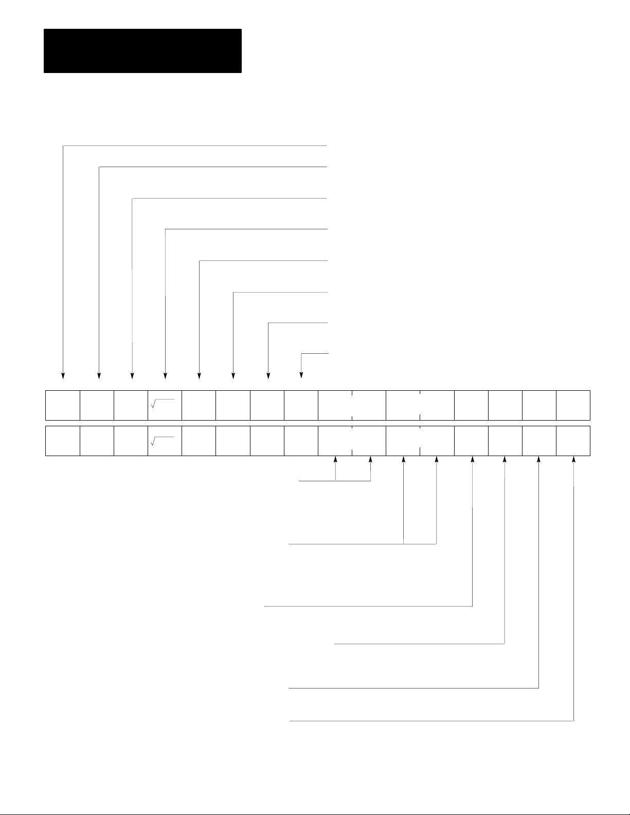
Chapter 3
Programming
Figure 3.6
W
Control
ord A, Loop 1 W18 and Loop 2 W38
W18 B17 Must be set to 0: W38 B17 must be set to 1
W18 B16 Must be set to 1: W38 B16 must be set to 0
W18(W38) B15 1=PV from PC Processor W09(W16)
0=PV from hardware analog input
W18(W36) B14 1=Perform square root of PV
0=No square root
W18(W38) B13 1=Error=(PVSP) reverse acting
0=Error=(SPPV) direct acting
W18(W38) B12 1=Use error limiting W21, W22 (W41, W42)
0=No limiting
W18(W38) B11 1=Use error dead band W23 (W43)
0=No dead band
W18(W38) B10 1=Use integral term limiting W26 (W46)
0=No limiting
Loop 1
W18
17 16 15 14 13 12 11 10 07 06 05 04 03 02 01 00
1
0
0
1
1
0
PC
1
PV1
PID
PC
0
PV2
PID
PV1
PV2
PV-SP
ERROR1
SP-PV
PV-SP
ERROR2
SP-PV
LIMIT
ERROR1
LIMIT
ERROR2
DEAD BAND
DEAD BAND
V1 MAX
LIMIT
V1 MAX
LIMIT
PROPORTIONAL
ERROR
FUNCTION
PROPORTIONAL
ERROR
FUNCTION
INTEGRAL
ERROR
FUNCTION
INTEGRAL
ERROR
FUNCTION
DERIV. ERR.
DERIV. ERR.
PV
PV
Error
Error
VD MAX
LIMIT
VD MAX
LIMIT
Loop 2
W38
W18(W38) B07,06 Proportional Error Function, E
0 0=Error
0 1=2/3 (Error) + 1/3 (Error)
1 0=1/3 (Error) + 2/3 (Error)
1 1= (Error)
2
P
2
2
HOLD
PID1
HOLD
PID2
HOLD
BIAS1
HOLD
BIAS2
W18(W38) B05,04 Integral Error Function, E
0 0=Error
0 1=2/3 (Error) + 1/3 (Error)
1 0=1/3 (Error) + 2/3 (Error)
1 1= (Error)
W18(W38) B03 Derivative Error, E
1=PV
0=Error
W18(W38) B02 1=Use derivative term limiting W27(W47)
0=No limiting
W18(W38) B01 1=Hold last V
0=Normal V
W18(W38) B00 1=Hold last BIAS value
0=Normal BIAS calculations
Note: If you change a loop 1 or loop 2
parameter, you must initiate a load/enter sequence
320
2
value
PID
calculations
PID
I
2
2
D
11109
Page 64

Chapter 3
Programming
W18 (W38) B12 Error Limit. Reset to 0 inhibits error limiting. Set
to 1 the maximum negative error term for the loop is limited to the
value EMN in word W21 (W41). The maximum positive error is
limited to value EMP in word W22 (W42).
W18 (W38) B11 Dead Band. Reset to 0 inhibits dead band. Set to
1 enables the dead band feature using the value in word W23 (W43).
Refer to word W23 (W43) Dead Band.
W18 (W38) B10 Maximum Integral Term Limit. Reset to 0
inhibits integral term limiting. Set to 1 the value of the integral term
V
is limited to the maximum value VI MAX in word W26 (W46).
I
This limit applies to both the negative and positive excursions of the
integral term V I.
W18 (W38) B07, B06 Proportional Term Error. The setting of the
2-bit code determines which error signal will be used for the
proportional term V
error term E
include straight error and error squared. Note that the
P
calculation. The choices of the proportional
P
sign is retained. The error codes are listed in Table 3.D.
W18 (W38) B05, B04 Integral Term Error. The setting of the 2-bit
code determines which error signal will be used for the integral term
V
calculation. The choices of the integral error term EI include
I
straight error and error squared. Note that the sign is retained. The
error codes are listed in Table 3.D.
W18 (W38) B03 Derivative Term Error. Reset to 0 the error signal
is used in the derivative calculation. Set to 1 the process variable
signal is used.
321
Page 65

Chapter 3
Programming
Table 3.D
Function Codes
Error
W18(W38)
V
P
V
I
B07
B05
0
0
1
1
B06
B04
Error Function
0
1
0
1
Error
2/3 (Error) + 1/3 (Error)
1/3 (Error) + 2/3 (Error)
2
(Error)
Error|Error|
Where (Error)2=_________
512
2
2
W18 (W38) B02 Maximum Derivative Term Limit. Reset to 0
inhibits derivative term limiting. Set to 1 the value of the derivative
term VD is limited to the maximum value VD MAX in word W27
(W47). This limit applies to both negative and positive excursions of
the derivative term VD.
W18 (W38) B01 Hold PID Calculation. Reset to 0 continues the
PID algorithm calculation. Set to 1 holds the PID algorithm output
VPID at its last value. The hold is useful when turning the
feedforward portion of the loop.
322
W18 (38) B00 Hold Bias. Reset to 0 continues the bias calculation.
Set to 1 holds the bias at its last value. The hold is useful when
tuning the PID portion of the loop.
W19 (W39) Loop Control Word B. This word together with loop
control word A, W18 (W38), and the loop expanded control word, W30
(W50), select the configuration for the loop. Bits 17 through 00 are
defined below and summarized in Figure 3.7 for loop 1 control word B
W19, and loop 2 control word B W 39. Note that bits B11, B10, B07, and
B06 are valid only if the expanded loop feature has been selected by W01
B14 = 1.
W 19 (W39) B17 VPID +/xBias. Reset to 0 the output is the sum V
= VPID + BIAS. Set to the output is the normalized product V =
(VPID x BIAS)/4095. The sum is normally used.
W19 (W39) B16 Output Limiting. Reset to 0 inhibits output
limiting. Set to 1 the analog output value is limited to the minimum
Page 66

Chapter 3
Programming
value VMIN in word W28 (W48) and the maximum value VMAX in
word W29 (W49). Limiting is not performed on the SET OUT value
in word W05 (W12).
W19 (W39) B15, B14, B13. Soft Fault Mode Selection. These bits
select the PID module’s response for the loop when communication
with the PC processor is broken. The PID module’s microprocessor
continues to operate and is firmware programmed to respond to the
fault. The PID module’s STAND-ALONE yellow LED indicator
flashes when the module is in the soft fault mode.
NOTE: In order for the PID module to operate in the soft fault
mode, the last state witch (switch 1) in the switch group assembly on
the I/O chassis backplane must be set to the off position. As such,
output of all other modules in the chassis will be de-energized when
a major fault is detected by the PC processor.
NOTE: When the PID module enters the soft fault mode, it does not
generate a manual request to relinquish control to the auto/manual
station. However, if the PID module detects a hardware failure when
in soft fault mode it will generate a manual request.
The soft fault operating modes are listed in Table 3.E.
323
Page 67
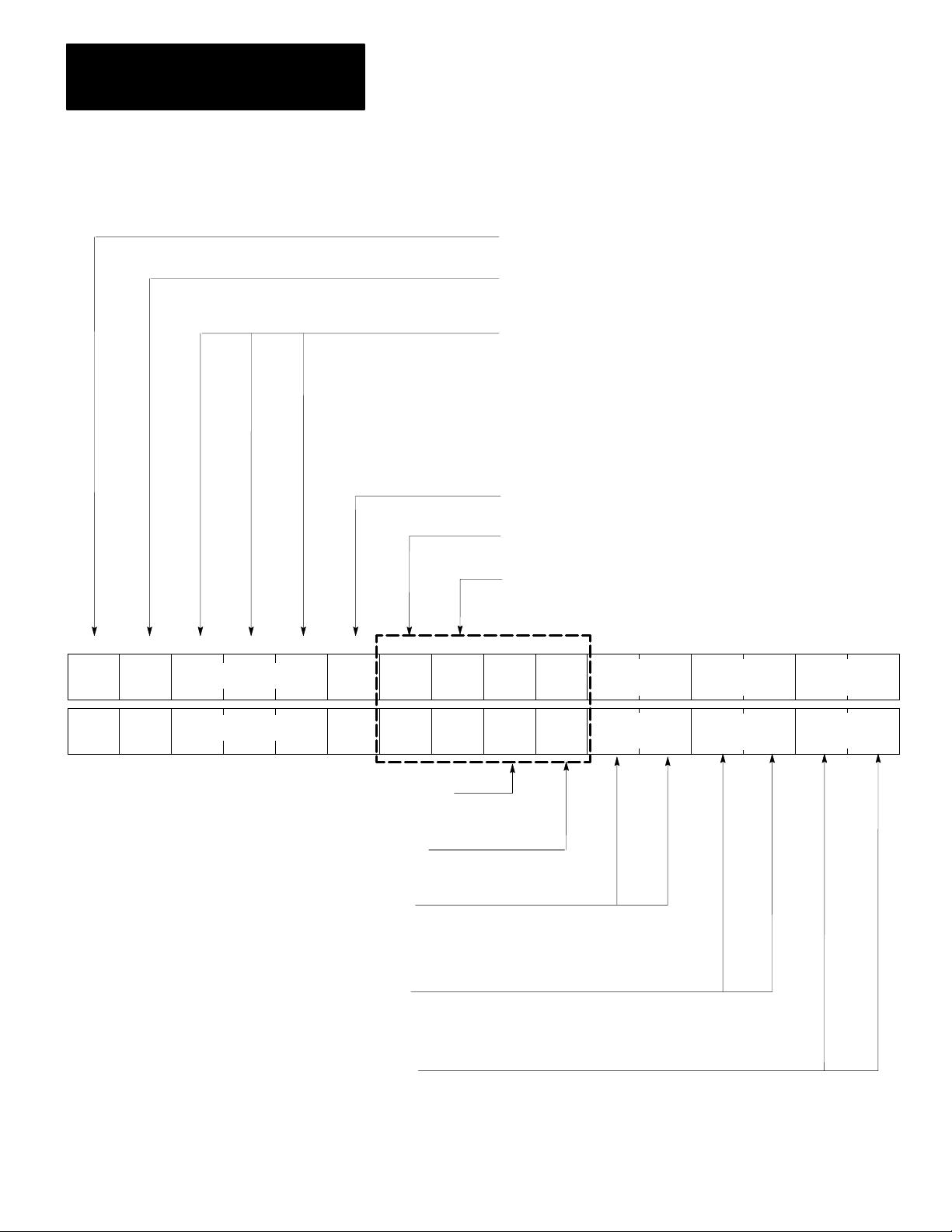
Chapter 3
Programming
Figure 3.7
W
Control
ord B, Loop 1 W19 and Loop 2 W39
PID
x BIAS
PID
+ BIAS
W19(W39) B17 1=Multiply V
0=Add V
W19(W39) B16
1=Use output limiting W28, W29,
(W48,W49)
0=No limiting
W19(W39) B15,14,13
SOFT FAULT MODE SELECTION
0 0 0 Output set to minimum value
0 0 1 Output holds last value
0 1 0 Output will hold Set Analog
Output value if W01 B01=1.
If W01 B01=0, module continues
to perform closed loop control
1 0 0 PID module will perform closed
loop control (ignores set output)
1 1 1 Output set to maximum value
W19(W30) B12
1=T
A W20(W40) times 10 (x10)
0=No multiplier (x1)
W19(W39) B1
1
1=TB W35(W55) times 10 (x10)
0=No multiplier (x1)
W19(W39) B10
1=TC W36(W56) times 10 (x10)
0=No multiplier (x1)
x10
TC1
x1
Expanded Loop
(-)
SP SIGN
(+)
x10
SCALING
x1
MULTIPLIER
FOR
1
K
p
MULTIPLIER
FOR
K 1
i
Loop 1
W19
17 16 15 14 13 12 11 10 07 06 05 04 03 02 01 00
MULT (X)
1
BIAS 1
SUM (+)
0
LIMIT
OUTPUT1
SOFT FAULT
SELECTION CODE
x10
TA1
x1
x10
TB1
x1
MULTIPLIER
FOR
1
K
D
1
0
Loop 2
W39
MULT (X)
BIAS 2
SUM (+)
LIMIT
OUTPUT2
SOFT FAULT
SELECTION CODE
W19(W39) B07 1=Negative scaled set point value
0=Positive scaled set point value
W19(W39) B06
1=Scaling values W31, W32,
(W51, W52) times 10 (x10)
0=No multiplier (x1)
W19(W39) B05,04
Multiplier for KP W07(W14)
0 0 K
0 1 K
1 0 K
1 1 K
W19(W39)
B03,02
Multiplier for KI W24(W44)
0 0 K
0 1 K
1 0 K
1 1 K
W19(W39)
B01,00
Multiplier for KD W25(W45)
0 0 K
0 1 K
1 0 K
1 1 K
Note: If you change a loop 1 or loop 2
parameter, you must initiate a load/enter sequence
P
P
P
P
I
I
I
I
D
D
D
D
x1
/10
x10
x100
x1
/10
x10
x100
x1
/10
x10
x100
x10
TA2
x10
TB2
x1
x1
x10
TC2
x1
(-)
SP SIGN
(+)
x10
SCALING
x1
MULTIPLIER
FOR
K
1
p
MULTIPLIER
FOR
K 1
i
MULTIPLIER
FOR
K
1
D
11110
324
Page 68

Chapter 3
Programming
Table 3.E
Multiplier
Codes
W19(W39)
B15 B14 B13
0 0 0
0 0 1
0 1 0
1 0 0
1 1 1
Soft Fault Operating Mode
Analog output is set to the minimum value (+4mA
or +1VDC).
Analog output holds the last value prior to the
fault.
The PID module performs closed loop control
unless W01 B01 = 1 for loop 1 (W01 B02= 1 for
loop 2). If this bit is set prior to the soft fault, the
SET OUT value in W05(W12) remains as the loop
output.
The PID module performs closed loop control
regardless of the status of W01 B01 (B02). If the
loop output was the SET OUT value in W05(W12)
when the soft fault occurred, the module reverts to
PID control. This mode should be selected for
interactive PC control.
Analog output is set to the maximum value
(+20mA or +5VDC)
Each loop must be set independently
. No other codes are permitted.
W19 (W39) B12 Input Filter Time constant Multiplier. Reset to 0
the multiplier for the input filter time constant TA stored in word
W20 (W40) is x1 (no multiplier). Set to 1 the multiplier is x10.
W19 (W39) B11 Lead Time Constant Multiplier. (XF) Reset to 0
the multiplier for the lead time constant TV stored in word W35
(W55) is x1. Set to 1 the multiplier is x 10.
W19 (W39) B10 Lag Time Constant Multiplier. (XF) Reset to 0
the multiplier for the lag time constant TC in word W 36 (W56) is
x1. Set to 1 the multiplier is x10.
W19 (W39) B07 Scaled Set Point Sign. (XF) Reset to 0 the set
point value in word W06 (W13) is positive. Set to 1 the value is
negative. This bit has meaning only when set point scaling has been
selected by 16 = 1 in word W30 (W50).
W 19 (W39) B06 Scaling Word Multiplier. (XF) This bit selects
the multiplier for the following words:
325
Page 69

Chapter 3
Programming
set point in word W06(W13)
minimum scaling value in word W31(W51)
maximum scaling value in word W32(W52)
loop error in word W62(W69)
read process variable in word W65(W72)
When this bit is reset to 0, the above values are multiplied x1. When
set to 1, the values in words W31(W51) and W32(W52) are
multiplied x10. The other words are multiplied x 10 only if the
values are scaled.
NOTE: The multiplier bit B06 must be examined to determine the
correct value of the loop error in word W62(W69) or the read
process variable in word W65(W72) when either word is read by the
PC processor.
W19(W38)B05, B04 Proportional Gain Multiplier. These two bits
select the multiplier for the integral gain K
in word W24(W44)(table
I
3.F).
W19(W39) B03, B02 Integral Gain Multiplier. These two bits
select the multiplier for the integral gain K
in word W24(W44)
I
(Table 3.F).
Table 3.F
Multiplier
K
K
K
K
Codes
P
I
D
F
W19(W39)
W19(W39)
W19(W39)
W30(W50)
B05
B03
B01
B07
0
0
1
1
B04
B02
B00
B06
0
1
0
1
Multiplier
X1
/10
x10
x100
W19(W39)B01, B00 Derivative Gain Multiplier. These two bits
select the multiplier for the derivative gain K
in word
D
W25(W45)(Table 3.F).
326
W20(W40)Input Filter Time Constant, TA. This word contains the
time constant for the input digital filter. The digital filter is the equivalent
of a single pole low pass filter. Data format is 4-digit BCD (99.99) with
Page 70

Chapter 3
Programming
an implied decimal point. the x10 multiplier bit is B12 in word
W19(W39). Range is 00.10 to 999.9. a value of zero implies no filter.
W21 (W41) Maximum Negative Error, EMN. This word contains the
maximum negative error for the loop. This value can be used for alarm
purposes and/or limiting. The alarm condition is indicated by
W61(W68)B15. error limiting is selected by B12 = 1 in word
W18(W38). Data format is 4-digit BCD with a range from 0000 to 4095.
a negative value is implied.
W22(W42) Maximum Positive Error, EMP. This word contains the
value used as the maximum positive error for the loop. This value can be
used for alarm purposes and/or limiting. The alarm condition is indicated
by W61(W68)B14. Error limiting is selected by B12 = 1 in word
W18(W38). Data format is 4-digit BCD with a range from 0000 to 4095.
a positive value is implied.
W23(W43) Dead Band, DB. This word contains the error dead band
value. This value can be used for alarm purposes and/or setting the dead
band range. The error dead band extends above and below zero error so
that the dead band range is twice the dead band value. Dead band is
selected by B11 = 1 in word W18(W38). The alarm condition is indicated
by W61(W68)B11. Data format is 4-digit BCD with a range from 0000 to
4095 above and below zero error.
Any time the error value is outside the dead band, the actual error value
will be used for computational purposes. As it crosses into the dead band,
the error value continues to be used for computational purposes until it
crosses zero. Once it crosses zero and as long as it remains in the dead
band, the error value will be set to zero for computational purposes.
W24(W44) Integral Gain, K I (Reset Term 1/T I). If W02B00 is reset,
the module uses the A-B value K I and this word contains the integral
gain constant for the loop. If W02 B00 is set, the module uses the ISA
value I/T I and the word contains the reset term for the loop. Data format
is 4-digit BCD, 9.999 in units of inverse seconds (A-B) or inverse minutes
(ISA), with implied decimal point. Multiplier bits W19(W39)B03, B02
can be selected for x1, divided by 10, x10, x100 (Table 3.F). By using
multipliers, the range can be extended from .0000 to 999.9.
The integral term K I or reset term 1/T I must be greater than zero for the
module to perform bumpless transfer. Reset or hold the integral term V I
to zero by setting K I or 1/T I = 0.
327
Page 71

Chapter 3
Programming
W25(W45) Derivative Gain, K D (Rate Term, Td). If W02 B00 is
reset, the module uses the A-B value K D and this word contains the
derivative gain constant for the loop. If W02 B00 is set, the modules uses
the ISA value Td and this word contains the rate term for the loop. Data
format is 4-digit BCD, 99.99 in units of seconds (A-B) or minutes (ISA),
with implied decimal point. Multiplier bits W19(W39)B03, B02 can be
selected by 1, divided by 10, x10, x100 (Table 3.F). By using multipliers,
the range can be extended from 0.000 to 9999.
W26(W46) Integral Term Limit, V I MAX. This word contains the
integral term limit for the loop. It can be used for alarm purposes and/or
limiting. The alarm condition is indicated by W61(W68)B10. Integral
term limiting is selected by B10 = 1 in word W18(W38). Data format is
4-digit BCD with a range from 0000 to 9999.
NOTE: When limiting is selected, lowering the value of V I MAX
reduces the PID module’s ability to adjust the integral term. The
performance of bumpless transfer could be hindered.
W27(W47) Derivative Term Limit, VD MAX. This word contains the
derivative term limit for the loop. It can be used for alarm purposes
and/or limiting. The alarm condition is indicated by W61(W68)B02.
Derivative term limiting is selected by B02 = 1 in word W18(W38). Data
format is 4-digit BCD with a range from 0000 to 9999.
W28(W48) Minimum Output Limit, VMIN. This word contains the
minimum limit for the analog output that is determined by the PID
module’s algorithm. This value can be used for alarm purposes and/or
limiting. The alarm condition is indicated by W61(W68)B01. Output
limiting is selected by B16 = 1 in word W19(W39). Data format is 4-digit
BCD with range from 0000 to 4095. This limit has no effect on a SET
OUT value downloaded from the PC processor into word W05(W12).
W29(W49) Maximum Output Limit, VMAX. This word contains the
maximum limit for the analog output that is determined by the PID
module’s algorithm. This value can be used for alarm purposes and/or
limiting. The alarm is indicated by W61(W68)B00. Output limiting is
selected by B16 = 1 in word W19(W39). Data format is 4-digit BCD with
a range from 0000 to 4095. This limit has no effect on a SET OUT value
downloaded from the PC processor into word W05(W12).
328
NOTE: The following words, W30(W50) through W36(W56), can be
programmed if the expanded features (XF) of the loop are selected by
Page 72

Chapter 3
Programming
W01 B14 = 1. The values of features not used must be zero. Section 3.6
describes expanded features such as cascade, decouple and feedforward.
W30(W50) Expanded Control Word (XF) This word together with
loop control word A, W18(W38), and loop control word B, W19(W39),
select the configuration for the loop. The expanded loop features are
active when selected by W01 B14 = 1. Bits 17 through 00 of the
expanded control word are defined below and summarized in Figure 3.8
for loop 1 word W30 and loop 2 word W50.
W30(W50)B17 Process Variable Scaling. (XF) Reset to 0 inhibits
process variable scaling. Set to 1 enables the scaling limits SMIN
and SMAX in words W32(W51) and W32(W52) respectively to
determine the scaled value of the process variable. The scaled or
unscaled process variable will be read by the PC processor in word
W65(W72). Refer to section titled Scaling for additional information
about scaling.
W30(W50)B16 Set Point Scaling. (XF) Rest to 0 inhibits set point
scaling. Set to 1 the module interprets this word as a scaled value
based on the scaling limits SMIN and SMAX IN WORD W32(W51)
and W32(W52), respectively. Refer to section titled Scaling for
additional information about scaling.
329
Page 73

Chapter 3
Programming
Figure 3.8
Expanded
Control W
Loop 1
W30
17 16 15 14 13 12 11 10 07 06 05 04 03 02 01 00
SCALE
1
PV1
SCALE
SP1
0
SCALE
1
PV2
SCALE
SP2
0
SCALE
ERROR1
SCALE
ERROR2
DECOUPLE0TIEBACK
FFI1
PC
TIEBACK
FFI2
PC
NEG.
FFI1
POS.
NEG.
FFI2
POS.
FFI1
FFI2
Loop 2
W50
W30(W50) B07,06 Multiplier for KF 34(W54)
x1
0 0 K
F
0 1 K
/10
F
x10
1 0 K
F
1 1 K
x100
F
ord, Loop 1 W30 and Loop 2 W50
W30(W50) B17 1=Use scaling for PV W65
W30(W50) B16 1=Use scaling for SP W06(W13)
W30(W50) B15 1=Use scaling for ERROR W62
W30(W50) B14 1=Decouple Loop 1 to Loop 2 in W30, only
W30(W50) B13 1=FFI from hardware Tieback input
W30(W50) B12 1=Change FFI to a negative value
W30(W50) B11 1=Perform square root FFI
W30(W50) B10 1=Multiply FF term by K
KFI X
[FFI+FF0]
KF2 X
[FFI+FF0]
MULTIPLIER
FOR
K
I
F
MULTIPLIER
FOR
I
K
F
LEAD/LAG
LEAD/LAG
0=No scaling, nonscaled value returned
0=No scaling, nonscaled value returned
0=No scaling, nonscaled value returned
0=No decoupling (Set W50 B14=0)
0=FFI from PC Processor W10(W17)
0=Maintain FFI as a positive value
0=No square root
0=No multiplication
F
(-)
SMIN1
(+)
(-)
SMIN2
(+)
(-)
SMAX1
(+)
(-)
SMAX2
(+)
PC
BIAS1
PID
PC
BIAS2
PID
NEG.
BIAS1
POS.
NEG.
BIAS2
POS.
CASCADE
LP1 TO
SP LP2
0
1
0
1
0
330
W30(W50) B05 1=Enabel lead/lag W35,36 (W55,W56)
0=No lead/lag
W30(W50) B04 1=Negative value for SMIN W31(W51)
0=Positive value for SMIN
W30(W50) B03 1=Negative value for SMAX W32(W52)
0=Positive value for SMAX
W30(W50) B02 1=Set BIAS from PC Processor W08(W15)
0=PID Algorithm BIAS(FFV)
W30(W50) B01 1=Change sign of BIAS(FFV)
0=Maintain sign
W30 B00 1=Cascade Loop 1 into Loop 2 (in W30 only)
0=No cascade (Set W50 B00=0)
Note: If you change a loop 1 or loop 2
parameter, you must initiate a load/enter sequence
11111
Page 74

Chapter 3
Programming
W30(W50)B15 Error Scaling. (XF) Reset to 0 inhibits loop error
scaling. Set to 1 enables the scaling limits SMIN and SMAX in
words W31(W51) and W32(W52) respectively to determine the
scaled value of the loop error. The scaled or unscaled loop error will
be read by the PC processor in word W62(W69). Refer to section
titled scaling for additional information about scaling.
W30(W50)B14 Decouple. (XF) Reset to 0 inhibits decoupling. Set
to 1 enables decoupling. The loop 1 PID calculation VPID 1 is used
for the feedforward input FFI to the loop 2 control algorithm.
Decoupling overrides the feedforward input FFI for loop 2. (W50
B14 for loop 2 must be reset to 0.) Refer to section titled Closed
Loop Control for additional information about decoupling.
W30(W50)B13 Source of Feedforward Input, FFI. (XF) Reset to
0 selects the value in word W10(W17) as the feedforward input for
the loop. Set to 1 selects the tieback input as the feedforward input.
W30(W50)B12 Feedforward Input Sign. (XF) Reset to 0
maintains the positive value of the feedforward input for the loop.
Set to 1 changes the value to negative.
W30(W50)B11 Feedforward Input Square Root. (XF) Reset to 0
inhibits the square root function. Set to 1 enables the normalized
square root of the feedforward input, (square root of FFI) x (square
root of 4095). Square root allows the linearization of differential
pressure type flow transducers.
W30(W50)B10 Feedforward Term Multiplication. (XF) Reset to
0 inhibits multiplication. Set to 1 enables the feedforward term
(feedforward offset + feedforward input) to be multiplied by the
feedforward gain in word W34(W54). The result is K
x (FFO +
F
FFI).
W30(W50)B07, 06 Feedforward Gain Multiplier. (XF) These
two bits select the multiplier for feedforward gain K
in word
F
W34(W54)(Table 3.F).
W30(W50)B05 Lead/Lag. (XF) Reset to 0 inhibits the lead/lag
function. Set to 1 enables the lead/lag function. The values for the
lead and lag time constants are contained in words W35(W55) and
W36(W56), respectively. Refer to section titled Lead/Lag Filter for
additional information about the lead/lag filter.
331
Page 75

Chapter 3
Programming
W30(W50)B04 Minimum Scaling Sign. (XF) Reset to 0 the sign
for SMIN in word W32(W51) is positive. Set to 1 the sign is
negative.
W30(W50)B03 Maximum Scaling Sign. (XF) Reset to 0 the sign
for SMAX in word W32(W52) is positive. Set to 1 the sign is
negative.
W30(W50)B02 Source of Bias. (XF) Reset to 0 the feedforward
value is the loop bias. Set to 1 the bias value in word W08(W15) is
the loop bias.
W30(W50)B01 Bias (FFV) Sign. (XF) Reset to 0 the sign of the
feedforward/bias term remains the same. Set to 1 the sign is
reversed.
W30(W50)B00 Cascade. (XF) Reset to 0 inhibits the cascade
feature. Set to 1 cascades the calculated output of loop 1 into the set
point of loop 2. (W50 B00 for loop 2 must be reset to 0). Refer to
section titled Closed Loop Control for additional information about
cascading.
W31(W51) Minimum Scaling Value SMIN. (XF) This word contains
the minimum (or bottom) scale value of the loop scaling algorithm. This
value is in engineering units. Data format is 4-digit BCD (9999
maximum). The sign bit B04 in word W30(W50) and the x10 multiplier
bit B06 in word W19(W39) must be considered to determine the value.
The range can be +
99990. Refer to section titled Scaling for additional
information about scaling.
W32(W52) Maximum Scaling Value, SMAX. (XF) This word contains
the maximum (or top) scale value of the loop scaling algorithm. This
value is in engineering units. Data format is 4-digit BCD (9999
maximum). The sign bit B03 in word W30(W50) and the x10 multiplier
bit B06 in word W19(W39) must be considered to determine the value.
The range can be +
99990. refer to section titled Scaling for additional
information about scaling.
332
W33(W53) Feedforward Offset, FFO. (XF) This word contains the
feedforward offset of the loop. It is added to the feedforward input. Data
format is 4-digit BCD (9999 maximum).
Page 76

Chapter 3
Programming
W34(W54) Feedforward Gain, K F. (XF) This word contains the
feedforward gain constant for the loop. Data format is 4-digit BCD
(99.99 dimensionless with implied decimal point. Multiplier bits B07,
B06 in word W30(W50) can be selected for x1, divided by 10, x10, 1100
(Table 3.F). The range can be 0.000 to 9999 when using the multipliers.
W35(W55) Lead Time Constant, TB. (XF) This word contains the lead
time constant for the loop. The lead/lag feature is selected by bit B05 in
word W30(W50). To disable the lead portion of the filter, reset TB to
zero. Data format is 4-digit BCD (99.99 in units of seconds) with implied
decimal point. By using the x10 multiplier bit B11 in word W19(W39),
the range can be 00.00 to 999.9.
W36(W56) Lag Time Constant, TC. (XF) This word contains the lag
time constant for the loop. The lead/lag feature is selected by bit B05 in
word W30(W50). To disable the lag portion of the algorithm, reset TC to
zero. Data format is 4-digit BCD (99.99 in units of seconds) with implied
decimal point. By using the x10 multiplier bit B10 in word W19(W39),
the range can be 00.00 to 999.9.
NOTE: There is no word number 37 to program. By omitting W37, the
storage words for loop 1 and loop 2 parameters are exactly 20 counts
apart.
Example: W20 Integral Gain 1 (W40 Integral Gain 2)
Status Block: W57W74
The status block is a read block transfer file of up to 18 words which is
used to report loop status, alarm and diagnostic information and to prompt
the proper block transfer sequences.
Only words W57 through W67 will be read if the module is selected for
loop 1 operation. The entire block (words W57 through W74) is read if
the module is selected for two-loop operation.
The 18 words that comprise the status block are defined in the paragraphs
that follow. Table 3.G lists the status block words. All the words of the
dynamic block, loop block and status block are listed in Table 3.J, in
Figure 3.13 and Figure 3.14 found at the end of section titled Word and
Bit Definitions.
333
Page 77

Chapter 3
Programming
Table 3.G
Block W
Status
ords
Both Loops
W57
W58
W59
W60
Loop 1
W61
W62
W63
W64
W65
W66
W67
Loop 2
W68
W69
W70
W71
W72
W73
W74
Word
Title Abbreviation
For future use
Alarm
Next Block Start Address
ime/Diagnostic
Loop T
Loop 1 Status
Loop 1 Error
Read Loop 1 Output
Read Analog Input 1
Read Process V
Read T
ieback Input 1
Read Feedforward V
Loop 2 Status
Loop 2 Error
Read Loop 2 Output
Read Analog Input 2
Read Process V
Read T
ieback Input 2
Read Feedforward V
ariable 1
alue 1
ariable 2
alue 2
ERROR1
READ V1
READ IN1
READ PV1
READ TIE1
READ FFV1
ERROR2
READ V2
READ IN2
READ PV2
READ TIE2
READ FFV2
W57 This word is reserved for future use. It will contain 0000.
W58 Alarm Word. This word contains alarm information for both
loops. It contains information concerning possible programming
errors and operating faults. Specific loop faults are found in the
status word W61 for loop 1 (W68 for loop 2). Bits 17 through 00 of
alarm word W58 are defined below and summarized in Figure 3.9.
W58 B17, B16 Block Identifiers. These two bits identify the status
block. Both bits will be read as 0 by the PC processor.
W58 B15 Dynamic Block Error. Set to 1 the previously transferred
dynamic block contained a programming error. To identify the error,
W01 B07 must be set to 1 so that the loop time/diagnostic word W60
can report diagnostic information. The upper byte of W60 will
contain the dynamic block error code. See word W60 below for
additional information.
W58 B14 Loop Block Error. Set to 1 the previously transferred
loop 1 or loop 2 block contained a programming error. To identify
334
Page 78

Chapter 3
Programming
the error, W01 B07 must be set to 1 so that the loop time/diagnostic
word W60 can report diagnostic information. The lower byte of
W60 will contain the error code. See word W60 below for additional
information.
W58 B13 Power-Up. After the PID module has received the first
valid dynamic block with the load bit W01 B06 =1, this bit will be
reset to 0. Note that this does not mean that the PID module is
programmed, only that the first dynamic block has been processed.
After the PID module has gone through its initial power-up
procedure or after the restoration of +5VDC, it will set bit W58 B13
to 1. This occurs when the module has cleared all internal memory
and is waiting to be programmed by block transfers to complete the
initial load/enter sequence. See section titled Power-Up Load/Enter
Sequence for additional power-up load/enter sequence information.
W58 B12 Ready. Set to 1 indicates that the load portion of the
load/enter sequence has been successfully completed. The ready bit
should be used to initiate the setting of the enter bit to complete the
sequence. After the enter bit is received by the PID module, the
ready bit will be reset to 0.
Before the enter bit is received by the PID module, a ready bit status
of 0 indicates an error was detected in either the dynamic block or a
loop block during the load portion of the load/enter sequence. The
error must be corrected before the ready bit can be set to 1. See
section titled Load/Enter Sequence or additional Load/enter sequence
information.
335
Page 79

Chapter 3
Programming
Figure 3.9
W
Alarm
ord W58
W58 B17 will be returned as 0
W58 B16 will be returned as 0
W58 B15 1=indicates programming error in the dynamic
block
W58 B14 1=indicates programming error in either loop 1 or
loop 2 block
W58 B13 1=in powerup mode
W58 B12 1=ready
W58
W58 B11 1=loss of +
15V dc power
W58 B10 1=in soft fault mode
17 16 15 14 13 12 11 10 07 06 05 04 03 02 01 00
1
0
DYNAMIC
BLOCK
0
ERROR
LOOP
BLOCK
ERROR
POWER-UP READY
LOSS OF
+ 15VDC
POWER
SOFT
FAULT
00 00 00 00
0
W58 B07B00 will be returned as 0
1
0
11112
336
Page 80

Chapter 3
Programming
W58 B11 Loss of +15VDC. Reset of 0 indicates that power is
present. Set to 1 indicates that the external +15VDC power is not
present. When +15VDC power is lost, the PID module generates a
manual request by closing the contact output.
W58 B10 Soft Fault Mode. Reset to 0 indicates that module is in
the normal operating mode. Set to 1 indicates the PID module is
operating in the soft fault mode. The soft fault response is
programmed by W19(W39) B15,14,13 (Table 3.E). Soft fault reset
is accomplished by setting W01 B10 to 1.
W58 B07 through B00. These bits are reserved for future use and
will be reset to 0.
W59 Next Block Start Address. The PID module controls the block
transfer programming sequences by determining which block should be
transferred next. This word contains the data table address of the first
word in the file associated with the next write block transfer. The PID
module reports to the PC processor the block start addresses programmed
in word W03 for the dynamic block, in word W04 for the loop 1 block, or
in word W11 for the loop 2 block. The PID module performs no data
manipulation on the next block start address in word W59.
W60 Loop Time/Diagnostic. This is a dual function word. This word
can report either the loop update time or diagnostic information. Its
function is established by W01 B07. When W01 B07 = 0, W60 reports
loop time. When W01 B07 = 1, W60 reports diagnostic information
(Figure 3.10).
When reporting loop time, the data format is 0-100 milliseconds. Bit
W60 B17 will be set to 1 to indicate when this word is reporting loop
time. The loop update time is nominally 100msec. The loop update time
is the time between successive module scans of the analog inputs. Only
one block transfer will be allowed during a loop update (Figure 3.11).
When reporting diagnostics, two separate error codes can be reported.
The error code is a 2-digit BCD value. The upper byte will indicate a
dynamic block error code. The lower byte will indicate a loop block error
code. If more than one error code exists, the first error code will be
displayed until it is corrected. Then the next error code will be displayed.
Table 3.H and Table 3.I contain error code definitions.
337
Page 81

Chapter 3
Programming
W61(W68) Loop Status. This word indicates various alarm conditions
for the corresponding loop and contains sign information for certain status
block words. Bits 17 through 00 of the loop status word are defined
below and summarized in Figure 3.12 for loop 1 word W61 and loop 2
word W68.
Figure 3.10
T
ime/Diagnostic Word W60
Loop
a) Loop time
Selected by W01 B07=0.
XYZ = Loop time in milliseconds
17161514131211100706050403020100
1000
XYZ
0
Read
Input
1
Read
Input
2
Calc
Output
1
b) Diagnostics
Selected by W01 B07=1
AB, CD = Diagnostic error codes
17161514131211100706050403020100
BCDA
Upper byte two digit
BCD code indicates
which word in the
dynamic block is in error.
Lower byte two digit
BCD code indicates which
word in the loop 1 or loop
2 block is in error
Figure 3.11
Loop
Calc
Output
2
Update T
Output
Set
1
ime
Set
Output
2
11113
100 msec
338
PID Algorithm Internal Housekeeping
Nominal Loop Update Time 100 msec
11114
Page 82

Table 3.H
Upper Byte Programming Error Codes
W60
Chapter 3
Programming
BCD Code
01
02
03
04
05
06
07
08
09
10
11
12
13
14
15
16
17
BCD Code
60
61
62
63
64
65
66
67
68
69
Dynamic Block W
Incorrect number of words for the dynamic block (1loop or
2loop configuration)
Not currently used as error code.
Not currently used as error code.
Not currently used as error code.
W05 is above maximum or has illegal BCD value.
W06 has illegal BCD value.
W07 has illegal BCD value.
W08 has illegal BCD value.
W09 has illegal BCD value.
W10 has illegal BCD value.
Not currently used as error code.
W12 is above maximum or has illegal BCD value.
W13 has illegal BCD value.
W14 has illegal BCD value.
W15 has illegal BCD value.
W16 has illegal BCD value.
W17 has illegal BCD value.
Dynamic Block W
Less than 10 words transferred (1loop configuration)
Less than 17 words transferred (2loop configuration).
Dynamic block identifier bits B17, B16 are not set correctly in
W01, and/or W18, and/or W38.
Less than 13 words transferred (1 loop configured with SET
OUT value of loop 2 requested).
Read and write block transfers are out of sequence. Status
block must be transferred first.
The load bit and enter bit must be set concurrently
The enter bit must not be set before the ready bit is returned
The verify and load bits must not be set concurrently
During the powerup load/enter sequence, the enter bit must be
set to complete the sequence.
During the load portion of the powerup load/enter sequence,
the dynamic block can be transferred only once.
ord Errors
ord Errors
.
.
339
Page 83

Chapter 3
Programming
Table 3.I
W60 Lower Byte Programming Error Codes
BCD Code
18
19
20
21
22
23
24
25
26
27
28
29
30
31
32
33
34
35
36
Dynamic Block W
Loop 1 constants block was not transferred in the load/enter
sequence.
W19 has illegal soft fault code 01
W20 has illegal BCD value.
W21 is above maximum or has illegal BCD value.
W22 is above maximum or has illegal BCD value.
W23 is above maximum or has illegal BCD value.
W24 has illegal BCD value.
W25 has illegal BCD value.
W26 has illegal BCD value
W27 has illegal BCD value.
W28 is above maximum or has illegal BCD value.
W29 is above maximum, has illegal BCD value, or is less than
W28.
W30 has cascade or decouple selected when only loop 1 is
selected.
W31 has illegal BCD value.
W32 has illegal BCD value or is less than or equal to W31
value..
W33 has illegal BCD value.
W34 has illegal BCD value.
W35 has illegal BCD value.
W36 has illegal BCD value.
ord Errors
1, 101, or 1
10.
BCD Code
38
39
40
41
42
43
44
45
46
47
48
49
50
51
52
53
54
55
56
Loop 2 Word Errors
Loop 2 constants block was not transferred in the load/enter
sequence.
W39 has illegal soft fault code o1
W40 has illegal BCD value.
W41 is above maximum or has illegal BCD value.
W42 is above maximum or has illegal BCD value.
W43 is above maximum or has illegal BCD value.
W44 has illegal BCD value.
W45 has illegal BCD value.
W46 has illegal BCD value.
W47 has illegal BCD value.
W48 is above maximum or has illegal BCD value.
W49 is above maximum, has illegal BCD value, or is less than
W48.
Not used
W51 has illegal BCD value.
W52 has illegal BCD value or is less than or equal to W51.
W53 has illegal BCD value.
W54 has illegal BCD value.
W55 has illegal BCD value.
W56 has illegal BCD value
1, 101, or 1
10.
340
Page 84

Chapter 3
Programming
BCD Code
70
80
81
82
Block T
ransfer Errors
Communication Fault. The number of block transfer words
exceeds the number expected by PID module.
Less than 12 words transferred in the standard loop constant
block.
Less than 19 words transferred in the expanded loop constants
block.
Loop 1 or loop 2 constants block can be transferred only in a
load/enter sequence.
341
Page 85

Chapter 3
Programming
Figure 3.12
Loop Status W
ord, Loop 1 W61 and Loop 2 W68
W61(W68) B17 1=ERROR W62(W68) has negative value
0=ERROR has positive value
W61(W68) B16 1=Scaled PV W65(W72) has negative value
0= positive value
W61(W68) B15 1=Error < EMN W21(W41)
W61(W68) B14 1=Error > EMP W22(W42)
W61(W68) B13 1=FFV has a negative value
0=FFV has a positive value
W61 B12 1=Load/enter sequence is complete, in W61
only.
W61(W68) B11 1=Error is within the dead band (W23)
0=Error is outside the dead band
W61(W68) B10 1=Integral term > V
MAX W26(W46)
I
Loop 1
W61
17 16 15 14 13 12 11 10 07 06 05 04 03 02 01 00
LOAD/
1
NEG.
ERROR1
POS.
0
1
NEG.
ERROR2
POS.
0
NEG.
SCALED PV
POS.
NEG.
SCALED PV
POS.
E<EMN1
E<EMN2
E>EMP1
E>EMP2
NEG.
FFV1
POS.
NEG.
FFV2
POS.
ENTER
COMPLETE
WITHIN
EROR
DEAD BAND
OUTSIDE
WITHIN
EROR
0
DEAD BAND
OUTSIDE
V > V
II
MAX
V > V
II
MAX
LOSS OF
ANALOG
INPUT 1
LOSS OF
ANALOG
INPUT 2
LOSS OF
TIEBACK
INPUT 1
LOSS OF
TIEBACK
INPUT 2
MANUAL
MODE
AUTOMATIC
MANUAL
MODE
AUTOMATIC
COMPLETE
POWER-UP
IN PROCESS
0
V >4095
P
V >4095
P
V > V
DD
MAX
V > V
DD
MAX
Loop 2
W68
W61(W68) B07 1=Loss of analog input
W61(W68) B06 1=Loss of tieback input
W61(W68) B05 1=Auto/manual station in the manual
mode
0=Loop is in the automatic mode under
PID module control
W61(W68) B04 1=Powerup sequence is complete, in
W61 only
0=In powerup mode; module is
unprogrammed
V<VMIN
V<VMIN
V>VMAX
V>VMAX
W61(W68) B03 1=Proportional term > 4095
W61(W68) B02 1=Derivative term > V
MAX W27(W47)
D
W61(W68) B01 1=Algorithm output < VMIN W28(W48)
W61(W68) B00 1=Algorithm output > VMAX W29(W49)
342
11115
Page 86

Chapter 3
Programming
W61(W68)B17 Sign of Loop Error. Reset to 0 the sign of the error
value in word W62(W69) is positive. Set to 1 the sign is negative.
W61(W68)B16 Sign of Read Process Variable. Reset to 0 the sign
of the scaled process variable in word W65(W72) is positive. Set to
1 the sign is negative. This bit has meaning only when process
variable scaling has been selected by W30(W50)B17 = 1.
W61(W68)B15 Error <Maximum Negative Error. Reset to 0 the
error value is greater than or equal to the maximum negative error
EMN in word W21(W41). Set to 1 the loop error is less than the
maximum negative error. The bit status is reported whether or not
error limiting is selected.
W61(W68)B14 Error>Maximum Positive Error. Reset to 0 the
error value is less than or equal to the maximum positive error EMP
in word W22(W42). Set to 1 the loop error is greater than the
maximum positive error. The bit status is reported whether or not
error limiting is selected.
W61(W68)B13 Sign of Feedforward Value. Reset to 0 the sign of
the feedforward value in word W67(W74)is positive. Set to 1 the
sign is negative.
W61(W68)B12 Load/Enter Complete. Reset to 0 when the module
receives a dynamic block transfer with the load bit W01 B06 = 1.
Bit B12 will be set to 1 at the completion of the load/enter sequence
after the module successfully processes the dynamic block with the
enter bit W01 B03 =1. The bit will remain set to 1 until a new
load/enter sequence is attempted. (W68 B12 in loop 2 will be
returned as 0.) Refer to sections titled Power-Up Load/Enter
Sequence and Load/Enter Sequence for additional information.
W61(W68)B11 Error within Dead Band. Reset to 0 the error for
the loop is outside the dead band established by the value in word
W23(W43). Set to 1 the error is inside the dead band. The bit status
is reported whether or not the dead band feature is selected.
NOTE: When the error enters the dead band range, the bit will not
be set until the error reaches (crosses) zero. It will be reset when the
error exceeds the dead band value.
343
Page 87

Chapter 3
Programming
W61(W68)B10 Integral Term>Integral Term Limit. Rest to 0 the
integral term V I is less than or equal to the integral term limit V I
MAX in word W26(W46). Set to 1 the integral term is greater than
V I MAX. The bit status is reported whether or not integral term
limiting is selected.
W61(W68)B07 Loss of Analog Input. Rest to 0 the analog input
signal from an input device is present and can be found in word
W64(W71). Set to 1 the hardware analog input is less than the
minimum value of +4mA or 1VDC. A loss of hardware analog input
will be detected whether or not a PV value is downloaded from the
PC processor into word W09(W16).
The loss of a hardware analog input will cause the corresponding
loop output to be held at its last value until the input is restored.
However, if the process variable has been downloaded from the PC
processor into word W09(W16), loss of a hardware analog input will
be detected but will not cause the analog output to be held.
NOTE: When downloading PC values from the PC processor when an
input device is not connected, jumper the INPUT (+LEAD) terminal to
the +15VDC terminal to prevent the loss of input bit W61(W68)B07 from
being set.
NOTE: Loss of input detection when analog inputs are configured in
voltage mode requires the use of 10K ohm 1/4 watt resistor. The resistor
must be connected between the INPUT (+LEAD) and (-LEAD) terminals
to ensure loss of input detection for an open or short circuit in one or both
leads of the input device. The module input impedance is thereby reduced
to 10k ohms. A resistor is not required for loss of input detection for
current mode analog inputs.
If either decoupling or cascading is selected and the hardware analog
input to loop 1 is lost, the output for both loops will be held
regardless of the status of the loop 2 inputs.
The loss of a hardware analog input is indicated by bit B07 of loop
status word W61(W68) and bit B02 of the status monitor byte.
344
W61(W68)B06 Loss of Tieback Input. Reset to 0 indicates that the
tieback input signal is present and can be found in word W66(W73).
Set to 1 indicates that the input is less than the minimum value of
+4mA or +1VDC.
Page 88

Chapter 3
Programming
The loss tieback input will cause the corresponding loop output to be
held at its last value until the input is restored.
If either decoupling or cascading is selected and the tieback input to
loop 1 is lost, the output for both loops will be held regardless of the
status of the loop 2 inputs.
When the tieback input is used as a hardware analog input, loss of
input detection does not require the use of an external resistor.
The loss of a tieback input is indicated by bit B06 or loop status word
W61(W68) and bit B02 of the status monitor byte.
W61(W68)B05 Manual Mode. Reset to 0 indicates that the PID
module is controlling the analog output signal to the actuator. Set to
1 indicates that the module has relinquished control to the user
supplied auto/manual station, placing the station in the manual mode.
Manual operation could have been initiated at the auto/manual
station by the loss of analog power, or by setting W01 B00 to 1.
W61(W68)B04 Power-Up Complete. Rest to 0 at power-up. After
a valid power-up load/enter sequence initializes the module, this bit
is set to 1. (W68 B04 for loop 2 will be reset.) Refer to section titled
Load/Enter Sequence for additional information.
W61(W68)B03 Proportional Term>4095. Reset to 0 indicates that
the proportional term V
(full scale). Set to 1 indicates that V
for the loop is less than or equal to 4095
P
is greater than 4095.
P
W61(W68)B02 Derivative Term>VD MAX. Reset to 0 indicates
that the derivative term VD for the loop is less than V
1 indicates that V
is greater than VD MAX IN W27(W47).
D
MAX. Set to
D
W61(W68)B01 ALGORITHM OUTPUT<Minimum Output.
Reset to 0 indicates that the analog output is in range and greater than
or equal to the minimum output value VMIN in word W28(W48).
Set to 1 indicates that the analog output computed by the PID module
is less than the VMIN. The bit status is reported whether or not
output limiting has been selected. This status bit does not monitor a
SET OUT value downloaded from the PC processor into word
W05(W12).
345
Page 89

Chapter 3
Programming
W61(W68)B00 Algorithm Output>Maximum Output. Reset to 0
indicates that the analog output is in range and less than or equal to
the maximum output value VMAX in word W29(W49). Set to 1
indicates that the analog output computed by the PID module is
greater than VMAX. The bit status is reported whether or not output
limiting has been selected. This status bit does not monitor a SET
OUT value downloaded from the PC processor into word
W05(W12).
W62(W69) Loop Error, ERROR. This word contains the loop error.
Data format is 4-digit BCD. The sign bit B17 in word W61(W668) can
establish an unscaled range of 0 to +
4095.
When error scaling is selected by W30(W50)B15 = 1, the loop error can
be reported in user-selected engineering units. The sign bit B17 in word
W61(W68) and the x 10 multiplier bit B06 in word W19(W39) must be
examined to determine the value. The scaled range can be +
99990. Refer
to section titled Scaling.
W63(W70) Read Loop Output, READ V. This word contains the final
analog output value as determined by the module’s PID algorithm. Data
format is 4-digit BCD or 12-bit binary. Format is selected by W01 B12.
Range is 0000 to 4095.
NOTE: When a SET OUT value is downloaded from the PC processor
into word W05(W12) by setting W01 B01(W01 B02) = 1, the SET OUT
value will override the analog output value. However, the value reported
in W63(W70) will always be the analog output value as determined by the
module’s PID algorithm, not the SET OUT value.
W64(W71) Read Analog Input, READ IN. This is the actual input
value read by the analog-to-digital converter in the module. Data format
is 4-digit BCD or 12-bit Binary. Format is selected by W01 B12. Range
is 0000 to 4095.
W65(W72) Read Process Variable, READ PV. This is the actual
process variable used by the PID module. Data format is 4-digit BCD.
The unscaled range is 0000 to 4095.
346
When process variable scaling is selected by W30(W50)B17 = 1, READ
PV can be reported in user-chosen engineering units. The sign bit B16 in
word W61(W68) and the x10 multiplier bit B06 in word W19(W39) must
Page 90

Chapter 3
Programming
be examined to determine the value. The range can be +99990. Refer to
section titled Scaling.
W66(W73) Read Tieback Input, READ TIE. This is the actual value read
by the analog-to-digital converter in the module. Data format is 4-digit
BCD or 12-bit binary. Format is selected by W01 B12. Range is 0000 to
4095.
W67(W74) Read Feedforward Value, Read FFV. This is the
feedforward computation as performed by the PID module. Data format
is 4-digit BCD with sign bit B13 in word W61(W68) allowing a range of
+
9999.
Control and status words are summarized in Figure 3.13, Figure 3.14 and
Table 3.J.
347
Page 91

Chapter 3
Programming
Figure 3.13
W
Control
Master Control Word W01
17 16 15 14 13 12 11 10 07 06 05 04 03 02 01 00
1
1
0
1
Loop 1 Control Word A W18
1
0
1
0
2 LOOPS
PC
PV1
PID
LOOP 1
EXPANDED
STANDARD
PV1
CALIB BINARY
PV-SP
ERROR1
SP-PV
LIMIT
ERROR1
BCD
ord Summary
BINARY
SP
BCD
DEAD BAND
SOFT
FAULT
RESET
V1 MAX
LIMIT
DIAG
LOOP
TIME
PROPORTIONAL
ERROR
FUNCTION
LOAD
VERIFY
CODE
00
INTEGRAL
ERROR
FUNCTION
ENTER
DERIV. ERR.
PV
Error
SET
OUTPUT 2
VD MAX
LIMIT
OUTPUT 1
SET
HOLD
PID1
MANUAL
REQUEST
HOLD
BIAS1
1
0
1
0
Loop 1 Control Word B W19
LIMIT
OUTPUT1
SOFT FAULT
SELECTION CODE
0
1
MULT (X)
BIAS 1
SUM (+)
Expanded Loop 1 Control Word W30
SCALE
1
PV1
SCALE
SP1
SCALE
ERROR1
0
Loop 2 Control Word A W38
1
1
0
PC
0
PV2
PID
Loop 2 Control Word B W39
1
0
MULT (X)
BIAS 2
SUM (+)
LIMIT
OUTPUT2
SELECTION CODE
DECOUPLE0TIEBACK
PV2
SOFT FAULT
FFI1
PC
PV-SP
ERROR2
SP-PV
x10
TA1
x1
NEG.
FFI1
POS.
LIMIT
ERROR2
x10
TA2
x1
x10
TB1
x1
FFI1
DEAD BAND
x10
TB2
x1
x10
TC1
I X
K
F
[FFI+FF0]
V1 MAX
LIMIT
x10
TC2
x1
x1
Expanded Loop
(-)
(+)
MULTIPLIER
FOR
K
I
F
ERROR
FUNCTION
x10
SCALING
SP SIGN
PROPORTIONAL
Expanded Loop
(-)
SP SIGN
(+)
x10
SCALING
1
HOLD
BIAS2
1
0
1
0
1
0
1
0
MULTIPLIER
LEAD/LAG
FOR
1
K
p
SMIN1
INTEGRAL
ERROR
FUNCTION
MULTIPLIER
FOR
K
1
p
(-)
(+)
x1
x1
MULTIPLIER
(-)
SMAX1
(+)
PV
DERIV. ERR.
Error
MULTIPLIER
FOR
K 1
FOR
K 1
i
BIAS1
VD MAX
i
PC
PID
LIMIT
NEG.
BIAS1
POS.
HOLD
PID2
MULTIPLIER
FOR
K
D
CASCADE
LP1 TO
SP LP2
MULTIPLIER
FOR
K
1
D
Expanded Loop 2 Control Word W50
K
2 X
SCALE
1
PV2
SCALE
SP2
0
SCALE
ERROR2
TIEBACK
FFI2
PC
NEG.
FFI2
POS.
FFI2
F
[FFI+FF0]
Note: If you change a loop 1 or loop 2 parameter, you must initiate a load/enter sequence.
348
MULTIPLIER
FOR
KFI
LEAD/LAG
(-)
SMIN2
(+)
(-)
SMAX2
(+)
PC
BIAS2
PID
NEG.
BIAS2
POS.
1
0
0
11116
Page 92

Chapter 3
Programming
Figure 3.14
W
Status
Alarm Word W58
17 16 15 14 13 12 11 10 07 06 05 04 03 02 01 00
1
0
DYNAMIC
BLOCK
0
ERROR
0
Status Monitor Byte SMB
LOOP
BLOCK
ERROR
POWER-UP READY
ord Summary
LOSS OF
+ 15VDC
POWER
SOFT
FAULT
00 00 00 00
07 06 05 04 03 02 01 00
AARM
00 1
CONDITION
POWERUP LOSS OF
AN INPUT
LOSS OF
+ 15VDC
POWER
SOFT
FAULT
MODE
1
0
Loop 1 Status Word W61
17 16 15 14 13 12 11 10 07 06 05 04 03 02 01 00
LOAD/
1
0
NEG.
ERROR1
POS.
NEG.
SCALED PV
POS.
E<EMN1
E>EMP1
NEG.
FFV1
POS.
ENTER
COMPLETE
WITHIN
EROR
DEAD BAND
OUTSIDE
V > V
II
MAX
LOSS OF
ANALOG
INPUT 1
LOSS OF
TIEBACK
INPUT 1
MANUAL
MODE
AUTOMATIC
COMPLETE
POWER-UP
IN PROCESS
V >4095
P
V > V
DD
MAX
Loop 2 Status Word W68
1
NEG.
ERROR2
POS.
0
NEG.
SCALED PV
POS.
E<EMN2
E>EMP2
NEG.
FFV2
POS.
WITHIN
EROR
0
DEAD BAND
OUTSIDE
V > V
II
MAX
LOSS OF
ANALOG
INPUT 2
LOSS OF
TIEBACK
INPUT 2
MANUAL
MODE
AUTOMATIC
V >4095
P
0
V > V
DD
MAX
V<VMIN
V<VMIN
V>VMAX
V>VMAX
11117
349
Page 93

Chapter 3
Programming
Table 3.J
ord Summary
W
DYNAMIC BLOCK
W01
W02
W03
Master Control W
Control W
Dynamic Block Start
Address
W04
W05
W06
W07
W09
W09
W10
W11
W12
W13
W14
W15
W16
W17
Loop 1 Block Start Address
Set Analog Output 1
Set Point 1
Proportional Gain 1
Bias 1
Set Process V
Set Feedforward Input 1
Loop 2 Block Start Address
Set Analog Output 2
Set Point 2
Proportional Gain 2
Bias 2
Set Process V
Set Feedforward Input 2
ord
ord
ariable 1
ariable 2
SET OUT1
SP1
K
1
P
BIAS 1
SET PV1
SET EFFI1
SET OUT 2
SP2
K
2
P
BIAS 2
SET PV2
SET FFI2
STA
TUS BLOCK
W57
W58
W59
W60
W61
W62
W63
W64
W65
W66
W67
W68
W69
W70
W71
W72
W73
W74
For Future Use
Alarm (both loops)
Next Block Start Address
Loop T
Loop 1 Status
Loop 1 Error
Read Loop 1 Output
Read Analog Input 1
Read Process V
Read T
Read Feedforward V
Loop 2 Status
Loop 2 Error
Read Loop 2 Output
Read Analog Input 2
Read Process V
Read T
Read Feedforward V
LOOP 1 BLOCK LOOP 2 BLOCK
W18
W19
W20
W21
W22
W23
W24
W25
W26
W27
W28
W29
W30
W31
W32
W33
W34
W35
W36
Loop 1 Control Word A
Loop 1 Control Word B
Input Filter Time Constant 1
Maximum Negative Error 1
Maximum Positive Error 1
Dead Band 1
Integral Gain 1
Derivative Gain 1
Integral T
Derivative T
erm Limit 1
erm Limit 1
Minimum Output Limit 1
Maximum Output Limit 1
Loop 1 Expanded Control
Word
Minimum Scaling V
Maximum Scaling V
Feedforward Of
alue 1
alue 1
fset 1
Feedforward Gain 1
Lead Time Constant 1
Lag T
ime Constant 1
TA1
EMN1
EMP1
DB1
1
K
I
K
1
D
V
MAX1
1
MAX1
V
D
VMIN1
VMAX1
SMIN1
SMAX1
FFO1
1
K
F
TB1
TC1
W38
W39
W40
W41
W42
W43
W44
W45
W46
W47
W48
W49
W50
W51
W52
W53
W54
W55
W56
Loop 2 Control Word A
Loop 2 Control Word B
Input Filter Time Constant 2
Maximum Negative Error 2
Maximum Positive Error 2
Dead Ban 2
Integral Gain 2
Derivative Gain 2
Integral T
Derivative T
Minimum Output Limit 2
Maximum Output Limit 2
Loop 2 Expanded Control
Word
Minimum Scaling V
Maximum Scaling V
Feedforward Of
Feedforward Gain 2
Lead Time Constant 2
Lag T
ime/Diagnostic
ariable 1
ieback Input 1
ariable 2
ieback Input 2
erm Limit 2
erm Limit 2
fset 2
ime Constant 2
alue 1
alue 2
alue 2
alue 2
ERROR1
READ V1
READ IN1
READ PV1
READ TIE1
READ FFV1
ERROR2
READ V2
READ IN2
READ PV2
READ TIE2
READ FFV2
TA2
EMN2
EMP2
DB2
2
K
I
K
2
D
V
MAX2
I
MAX2
V
D
VMIN2
VMAX2
SMIN2
SMAX2
FFO2
2
K
F
TB2
TC2
Note: If you change a loop 1 or loop 2 parameter
350
, you must initiate a load/entry sequence.
Page 94

Chapter 3
Programming
Algorithm Flow Chart
The algorithm flow chart shows the selectable features of the PID
module’s control algorithms and indicates how selected features effect the
entire algorithm.
The algorithm flow chart can be used as a road map when programming
the PID module. Begin at the analog input. Select the needed features.
Record their word and bit values on copies of the worksheet found in
appendix A. When all needed features have been selected and the flow
chart has been followed to completion, the selections can be entered into
appropriate files in the PC processor. Data entry can be done after data
table addresses have been assigned to the data block and the ladder
diagram program has been entered into memory.
Prior to following the flow chart, there are five decisions concerning
module features which must be made. These decisions and their
corresponding control bits are not on the chart.
1-loop or 2-loop operation, W01 B15
standard or expanded features, W01 B14
4-digit BCD or 12-bit binary data format for most analog terms, W01
B12
4-digit BCD or 12-bit binary data format for the set point, W01 B11
soft fault response for each loop W38(W59) B15,14,13
Block Transfer Programming
The algorithm flow chart is shown in Figure 3.15. Sheet 1 shows,
callouts, abbreviations, and how to interpret the flow chart. See Appendix
E for an enlarged fold-out of the flow chart.
This section describes how the PID module is programmed. It also
describes how the status of the PID module can be continuously read by
the PC processor without performing read block transfers. Programming
techniques and strategies are explained in this section. Example
program/applications are presented in appendicies B and C. The
programming explanations pertain to the PLC-2/30 processor. Programs
can be modified for other processors capable of block transfer (refer to
chapter 1).
351
Page 95

Chapter 3
Programming
WORD / BIT CALLOUTS
SMIN ABBREVIATION FOR MINIMUM SCALING VALUE
+
9999
W31 (W51)
W19 B06
M
S
B/B
NO
YES
RANGE OF VALUES
PID MODULE WORD NUMBER. LOOP 1 (LOOP 2)
BIT NUMBER. (LOOP 2 NUMBERS ARE IN PARENTHESIS.)
PREFIX M MEANS MULTIPLER BIT(S).
PREFIX S MEANS SIGN BIT.
PREFIX B/B REFERS TO BCD/BINARY FORMAT BIT.
LOGIC STATE 0
LOGIC STATE 1
SYMBOLS
Figure 3.15
Algorithm
FUNCTION
DECISION
WRITE BLOCK TRANSFER
FROM PC PROCESSOR
READ BLOCK TRANSFER
TO PC PROCESSOR
Flow Chart (3 sheets)
THE ALGORITHM FLOW CHART CONSISTS OF TWO PAGES WHICH FOLLOW ON SHEETS 2 AND 3.
THEY ARE SHOWN BELOW IN ABBREVIATED FORM TO PRESENT THE GENERAL SIGNAL FLOW AND TO DEFINE THE SYMBOLS
AND CALLOUTS USED THROUGHOUT. THE BOX AT THE UPPER LEFT DESCRIBES THE WORD/BIT CALLOUTS. THE BOX JUST
BELOW DEFINES THE SYMBOLS.
THERE ARE FIVE FEATURES NOT SHOWN ON THE CHART THAT SHOULD BE SELECTED BEFOREHAND:
1. ONE OR TWO LOOP OPERATION W01 B15
2. STANDARD OR EXPANDED FEATURES W01 B14
3. FOURDIGIT BCD OR 12BIT BINARY FORMAT FOR SETPOINT, W01 B11
4. FOURDIGIT BCD OR 12BIT BINARY FORMAT FOR ANALOG VALUES, W01 B12
5. SOFT FAULT RESPONSE FOR EACH LOOP, W39 (W59) B15, B14, B13
THE ALGORITHM FLOW CHART CAN BE USED AS A ROAD MAP WHEN PROGRAMMING. BEGIN AT THE ANALOG INPUT
AND FOLLOW THE CHART TO DETERMINE WHICH FEATURES SHOULD BE IMPLEMENTED.
AA
LEGEND SHEET
DOUBLE LINE SYMBOLS MEAN
EXPANDED FEATURES
(SINGLE LINE MEANS
STANDARD FEATURES)
GO-TO AND RECEIVE-FROM
LABELS WITHIN AND BETWEEN
PAGES
HARDWARE OUTPUTS
AND INPUTS
SMIN
+
9999
W31 (W51)
MW19 B06
(MW39 B06)
SW30 B04
(SW50 B04)
SHEET 2
START
EXPANDED
FEATURES
SHEET 3
ENTER
MAX/MIN VALUES
START
FEEDFORWARD
INPUT W10 (W17)
B/B W01 B12
ENTER TIEBACK
V
PID
ANALOG
INPUT
C
YES
TIEBACK
V
ERROR
YES
READ
PV
SCALE
FFI
OR
S
EXPAND
LOOP
ENTER BIAS
EXPAND
LOOP
NO
A
BIAS
W08 (W15)
C
A/D
A
P
I
D
K
D
STANDARD
FEATURES
STANDARD
FEATURES
SP
SPV
V
PID
S
ANALOG
OUTPUT
TIEBACK
INPUT
11118
352
Page 96
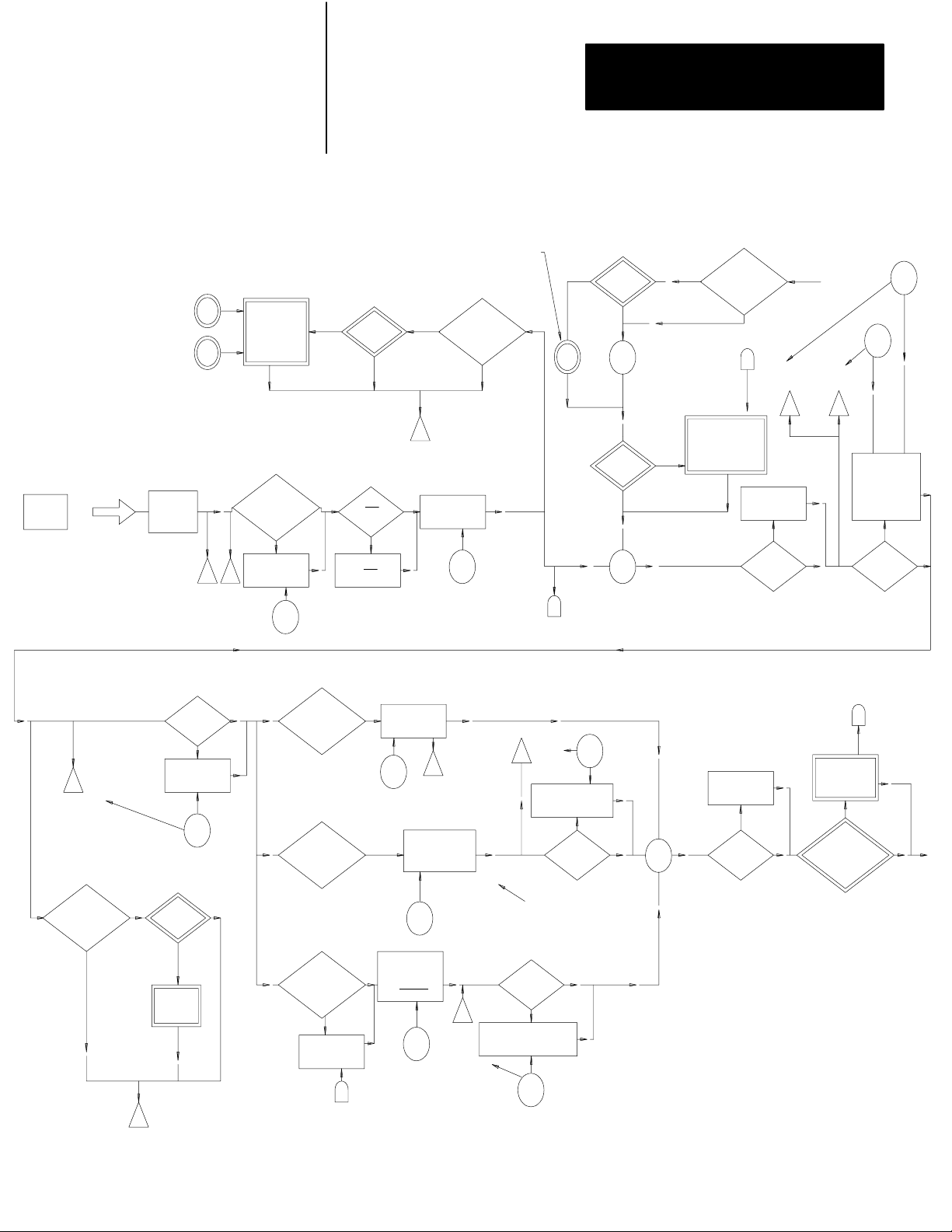
START
PV
HARDWARE
ANALOG
INPUT
S MAX
+
9999
W32 (W52)
MW19 B06
(MW39 B06)
S W30 B03
(S W50 B03)
A/D
LOSS OF
INPUT
W61 B07
(W68 B07)
S MIN
+
9999
W31 (W51)
MW19 B06
(MW39 B06)
SW30 B04
(SW50 B04)
ANALOG
INPUT
4095 B/B
W01 B12
W64 (W71)
ENTER MIN
AND MAX
SCALING
VALUES
W18 B15
(W38 B15)
USE PV
FROM PC
PROCESSOR
USE VALUE
FROM PC
YES
PC PV
4095 B/B W01 B12
W09 (W16)
YES
W18 B14
(W38 B14)
NO
PERFORM
(NORMALIZED)
W30 B17
(W50 B17)
PV
SCALING
PV
/
PV
/
NO
YES
YES
(EXPANDED)
(EXP)
NO
W01 B14
EXPANDED
LOOP
SELECTED
READ PV
W65 (W72)
SW61 B16
(SW68 B16)
DIGITAL
FILTER
TA
99.99
W20 (W40)
MW19 B12
(MW39 B12)
TA 0 MEANS OFF
SP
+
9999
W06 (W13)
MW19 B06
(MW39 B06)
SW19 B07
(SW19 B07)
NO
(STANDARD)
YES
PV
TO DERIVATIVE
A
FUNCTION
SHEET 2
Chapter 3
Programming
W30 B16
(W50 B16)
YES
(EXPANDED)
SP
SCALING
NO
SP
4095 B/B
W01 B11
W06 (W13)
CASCADE
LOOP 2 ONLY
ENABLED BY W30 B00
SP
(+)
(-)
E = SP - PV
S
W01 B14
EXPANDED
LOOP
SELECTED
FROM
CASCADE
SHEET 3
CASCADE LOOP
1 TO LOOP 2
LOOP VALUE
ENTERS HERE
CHANGE
TO
E=PV-SP ?
NO
(STANDARD)
D
E<EMN
W61 B15
(W68 B15)
X(-1)
YES
W18 B13
(W38 B13)
E>EMP
W61 B14
(W68 B14)
E=PV-SP
NO
E=SP-PV
SP
EMN
W21 (W41)
4095
EMP
W22
(W42)
4095
IF E<EMN
THEN E=EMN
IF E>EMP
THEN E=EMP
YES
ERROR
LIMIT
W18 B12
(W38 B12)
NO
E
DB
3
W61 B11
(W68 B11)
EXPANDED
LOOP
FEATURES
NO
(STANDARD)
YES
(EXP)
W18 B11
(W38 B11)
IF E
THEN E = 0
ERROR
SCALING
YES
USE
FUNCTION
ERROR
+
9999
W62 (W69)
SW61 B17
(SW68 B17)
DEAD
BAND
YES
3
ZERO
CROSSING
DEAD BAND
4095
W23 (W43)
W18 B07 B06
(W38 B07 B06)
NO
DB
NO
CHOOSE
ERROR
FUNCTION
CHOOSE
ERROR
FUNCTION
W18 B03
(W38 B03)
CHOOSE
ERROR
OR PV
USE PV
FROM PV
SHEET 2
YES
E
KP
99.99
W07 (W14)
MW19 B05 B04
(MW39 B05 B04)
E
DERIVATION
E
FUNCTION
NO
PV
A
PROPORTIONAL
FUNCTION
Kp ( )
V
P
V1
I V1 1
.
MAX
W61 B10
(W68 B10)
I VP I > 4095 HOLD LAST
W61 B03
(W68 B03)
INTEGRAL
FUNCTION
> k1 ( )
t
D
IF K1=0 TERM
SET TO 0
K1
9.999
W24 (W44)
MW19 B03 B02
(MW39 B03 B02)
( )
D
KD
t
D
I VD 1 > VD
MAX
THEN I VD I = VD MAX
W61 B02
(W68 B02)
KD
99.99
W25 (W45)
MW19 B01 B00
(MW39 B01 B00)
I V1 1
THEN I V1 I = V1
MAX
BUMPLESS TRANSFER
AND HOLDS ARE
PERFORMED HERE
LIMIT
VD MAX
YES
I VD I > VD MAX
NO
VD MAX
W27 (W47)
V1 MAX
W26 (W46)
V1 MAX
.
LIMIT
VD MAX
YES
V
I
NO NO
W18 B10
(W38 B10)
S
V
V
D
PID = V
P
+ V
PERFORM
BUMPLESS
TRANSFER
VALUE
HOLD
V
PID
+ V
I
D
YES
W18 B01
(W38 B01)
SEND LOOP1
VALUE TO
LOOP 2
YES
DECOUPLE
LOOP 1 TO
LOOP 2
B
LOOP 1
ONLY.
ENABLED
11119
TO SHEET 3
DECOUPLE
V
PID
BY W30
B14
NO
V
PID
TO
SHEET
3
353
Page 97

Chapter 3
Programming
START
EXPANDED
FEATURES
SET
FEEDFORWARD
INPUT W10 (W17)
4095 B/ B 12
W30 B13
(W50 B13)
PC FFI
OR
TIEBACK
YES
VALUE FROM
TIEBACK
C
TIEBACK
INPUT
FROM SHEET 3
BIAS (FFV)
(FROM PC)
NO
LOOP2
ONLY.
ENABLED
BY W30
DECOUPLE
YES
IF DECOUPLING
WAS SELECTED
VALUE IS
INPUT HERE
B
DECOUPLE
V
PID
FROM SHEET 2
B14
W30 B11
(W50 B11)
FFI
/
YES YES
PERFORM
SQUARE
ROOT
(NORMALIZED)
W18 B00
(W38 B00)
NO
HOLD LAST
NO
HOLD
BIAS
(FFV)
YES
BIAS (FFV)
W30 B12
(W50 B12)
CHANGE
SIGN
X(-1)
YES
(EXPANDED)
FFI
NO
FEEDFORWARD
OFFSET (FF0)
9999
W33 (W53)
W01 B14
EXPANDED
LOOP
SELECTED
NO
(STANDARD)
ENTER
BIAS
(BIAS ENTRY
STANDARD LOOP)
S
FFI+FF0
K
F
99.99
W34 (W54)
MW30 B07, 06
(MW50 B07, 06)
W30 B10
(W50 B10)
BIAS
9999
W08 (W15)
X (K )
F
X K
STANDARD
FEATURES
F
YES
W30 B05
(W50 B05)
NO
K (FF0
+ FFI)
PERFORM
LEAD-LAG
TB
I
TB
99.99
W35 (W55)
MW19 B11
(MW39 B11)
TCS +1
TB=0 TC=0 MEANS OFF
THE PATH TO THIS
POINT HAS MEANING
ONLY WHEN EXPANDED
FEATURES ARE SELECTED
READ
FEEDFORWARD VALUE
.9999
W67 (W74)
(SW68 B13)
SW61B13
NO
YES
+1
S
TC
99.99
W36 (W66)
MW19 B10
(MW39 B10)
W30 B02
(W50 B02)
FFV
OR
PC BIAS
YES
SET THRU
PC
BIAS
9999
W08 (W15)
BIAS ENTRY
(EXPANDED LOOP)
W30 B01
(W50 B01)
NO
CHANGE
SIGN
YES
NO (FFV)
X(-1)
FROM
SHEET
2
1: V=(V ) (BIAS)
0: V=V + BIAS
LOOP 2
W19 B16
(W39 B16)
V
PID
PID
4095
PID
+/X
W19 B17
(W39 B17)
V < V MIN
W61 B01
(W68 B01)
V
IF V
V MIN, SET
V=V MIN
IF V
V > V MAX
W61 B00
(W68 B00)
V MAX, SET
V=V MAX
OUTPUT
LIMIT
3
.
V MAX
4095
W29
(W49)
YES
NO
V MIN
4095
W28 (W48)
ONLY.
ENABLED BY
W30 B00
CASCADE
SEND VALUE
OF LOOP 1
TO SP OF
LOOP 2
TO CASCADE
SHEET 2
YES
D
TO FEEDFORWARD
LW30 B13
(W50 B13)
SHEET 3
ANALOG TIEBACK INPUT
4095 B / B W01 B12
VALUE W66 (W73)
NO
READ V
W63 (W70)
4095 B / B
W01 B12
W01 B01 (LOOP 1)
W01 B02 (LOOP 2)
SET
DIRECT
BUMPLESS
YES
TRANSFER
SET ANALOG
OUTPUT
FROM PC
VALUE
SET ANALOG
OUTPUT
4095 B/B W01 B12
W05 (W12)
C
NO
W61 B05 (LOOP 1)
W68 B05 (LOOP 2)
LOSS OF TIEBACK
INPUT
W61 B06
(W68 B06)
D / A
MANUAL
REQUEST
W01 B00
(ONE SHOT)
HARDWARE
SET BY PID
A / D
FAULT
MODULE
HARDWARE
ANALOG
OUTPUT
MAN/AUTO
TIEBACK ANALOG INPUT
MANUAL
REQUEST
SINGLE
OUTPUT
V
AUTO/
MANUAL
STATION
(OPTIONAL)
TO CONTROL
DEVICE
11120
354
Page 98

Chapter 3
Programming
Block Transfer Instruction Overview
All programming data for the PID module must be contained in files
residing in the PC processor’s data table. The files are block transferred
to the PID module where they are stored and used to perform PID control.
Figure 3.16 and Figure 3.17 present a brief summary of block format
block transfer instructions and data table locations.
NOTE: For PLC-2 family processors, the address of the file to be
transferred in the address of the first word in the file. The file address is
stored in BCD in a storage word located 100 8 above the instruction’s data
address. The number of words transferred must vary according to the
number of words in any of the files. When the block length is set to the
default value, the PID module will control the block length for each
transfer. Otherwise, if a program is written that allows unequal block
length other than default to be enabled in the same scan, incomplete data
could be transferred.
Figure 3.16
Block
Format Block T
A block transfer instruction is
programmed in the ladder diagram by
deptressing the [BLOCK XFER] key
followed by [1] (for a READ) or [0] (for a
WRITE). The appropriate read or write
block, as shown below will appear on the
industrial terminal screen.
Numbers shown are default values.
Numbers in shaded areas must be
replaced by userentered values. The
number of default address digits initially
displayed, 3, 4, or 5 will depend on the
size of the data table. Initially displayed
default values are governed by the I/O
rack configuration.
Data Address : First, possible address in accumulated value area of data table.
Module Address : Rack, module group, and slot number.
Block Length : Number of words to be transferred. (00 can be entered for default value or for 64 words)
File : Address of first word in the file. Storage location is 100
Enable Bit (EN) : Automatically entered from the module address. Set on when rung containing the
instruction is true.
Done Bit (DN) : Automatically entered from the module address. Remains on for 1 scan following
successful transfer.
ransfer Instructions
BLOCK XFER READ
DATA ADDR:
MODULE ADDR:
BLOCK LENGTH:
FILE:
BLOCK XFER WRITE
DATA ADDR:
MODULE ADDR:
BLOCK LENGTH:
FILE:
above the data address.
8
030
100
110 110
030
100
110 110
01
01
0130
EN
07
110
DN
07
010
EN
06
110
DN
06
11121
355
Page 99

Chapter 3
Programming
RW
1
1
Data Table
1
1
Figure 3.17
Example Data T
RW
BLOCK LENGTHCODE
1
1
3
3
RW
1
1
able Locations for Bidirectional Block T
010
013
Output image table low byte
0
0
040
Data Addresses contains the module
address 130: rack 1, module group 3, slot 0.
041
Input image table low byte
113
R=Read bit
W=Write bit
ransfer
2
2
Read Block Transfer
(Input Buffer)
Write Block Transfer
3
5
File
File
3
7
140
Storage locations of file addresses
141
233
By setting the block length to default, 00,
the module will determine the number of words
up to 64 to be read to the PC processor.
256
257
By setting the block length to default, 00,
the module will determine the number of words
up to 64 to be written from the PC processor
to the module.
356
BLOCK TRANSFER READ
DATA ADDR:
MODULE ADDR:
BLOCK LENGTH:
FILE:
BLOCK TRANSFER WRITE
DATA ADDR:
MODULE ADDR:
BLOCK LENGTH:
FILE:
040
130
233 332
041
130
257 356
00
00
013
EN
07
013
DN
07
013
EN
07
113
DN
07
11122
356
Page 100

Chapter 3
Programming
Those unfamiliar with block transfer programming techniques should read
the explanation found in the programming and Operation Manual for the
PC processor being used. It is important to under block transfer concepts
before reading this section.
Block Transfer Sequencing
The PID module is designed to sequence the multiple block transfers
required to program the module and actively communicate with the PC
processor. The PID module can prompt a block transfer sequence by
sending to the PC processor the data table address of the first word in the
file to be transferred next in the sequence. A rung in the ladder diagram
program is required to manipulate the file address in the write block
transfer instruction.
The data table address of each of the three data blocks is written to the
PID module in the dynamic block transfer. One word defines the starting
address of each block:
W03 dynamic block start address
W04 loop 1 block start address
W11 loop 2 block start address
The PID module returns to the PC processor the data table address (next
block start address) of the next block to be transferred. The address is the
value in word W59 in the status block. Two rungs are required to perform
the prompting (Figure 3.18). During normal operation rung A gets the
value returned by the PID module in word W59 and puts it in the file
address storage word of the write block transfer instruction. The user
program automatically performs the next block transfer required in the
sequence determined in this manner by the PID module.
Rung B is active only at power-up. If the module is in the power-up mode
and is unprogrammed, it cannot automatically prompt a block transfer.
Instead, the PID module returns the power-up bit W58 B13 = 1 to a data
table storage bit such as 350/13. The power-up bit controls rung B. At
power-up only, rung B forces the write block transfer instruction to
transfer the dynamic block. The dynamic block contains the block start
address for each of the three write blocks. After the PID module receives
this transfer, it can control the sequencing with rung A.
357
 Loading...