

Page 1
Page 2

T
able of Contents
Introduction 1-1 . . . . . . . . . . . . . . . . . . . . . . . . . . . . . . . . . . . . . .
General 1-1
Typical
. . . . . . . . . . . . . . . . . . . . . . . . . . . . . . . . . . . . . . . . . . . . . . . . . .
Applications
. . . . . . . . . . . . . . . . . . . . . . . . . . . . . . . . . . . . . . . . . .
1-2
Module Preparation, Wiring and Installation 2-1 . . . . . . . . . . . . . .
General 2-1
Switch
Wiring 2-4
Additional
Keying 2-11
. . . . . . . . . . . . . . . . . . . . . . . . . . . . . . . . . . . . . . . . . . . . . . . . . .
Selection of Operating Modes
. . . . . . . . . . . . . . . . . . . . . . . . . . . . . . . . . . . . . . . . . . . . . . . . . . . .
Considerations
. . . . . . . . . . . . . . . . . . . . . . . . . . . . . . . . . . . . . . . . . . . . . . . . . . .
. . . . . . . . . . . . . . . . . . . . . . . . . . . . . . . . . . . . . .
. . . . . . . . . . . . . . . . . . . . . . . . . . . . .
2-1
2-10
Programming and Operation 3-1 . . . . . . . . . . . . . . . . . . . . . . . . . .
General 3-1
Module Scan of Switch Contacts
Storage
Block
. . . . . . . . . . . . . . . . . . . . . . . . . . . . . . . . . . . . . . . . . . . . . . . . . .
. . . . . . . . . . . . . . . . . . . . . . . . . . . . . . . . .
of Switch Contact Data
T
ransfer of Switch Data
. . . . . . . . . . . . . . . . . . . . . . . . . . . . . . . . .
. . . . . . . . . . . . . . . . . . . . . . . . . . . . . . . . . . .
3-1
3-1
3-14
Specifications A-1
. . . . . . . . . . . . . . . . . . . . . . . . . . . . . . . . . . . . .
i
Page 3

T
able of Contents
ii
Page 4
Introduction
Chapter
1
General
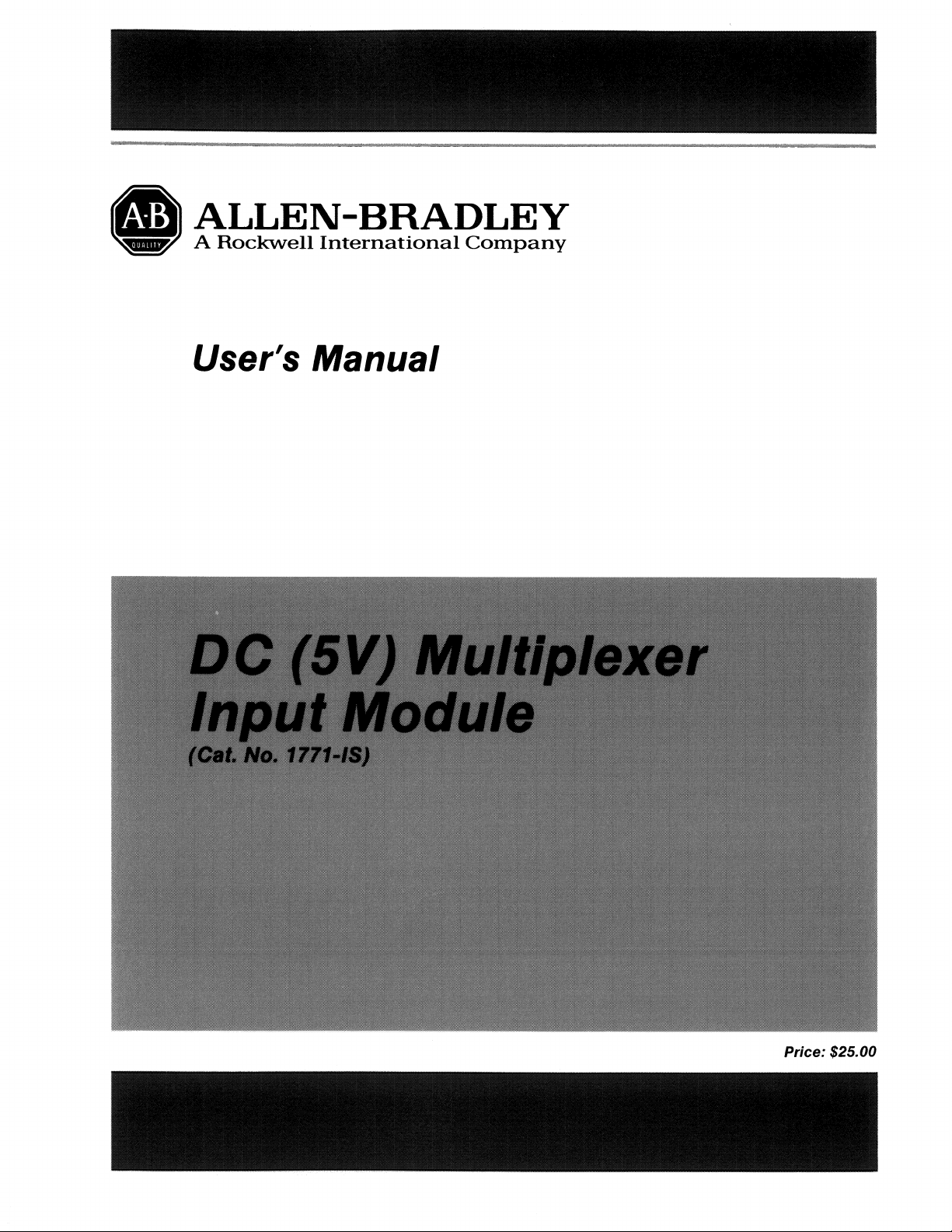
The 1771-IS DC (5V) Multiplexer Input Module, Figure 1.1 reads the
status of up to 72 hard contact switch devices through one I/O slot. This
information is transferred to the PC processor by block transfer
programming. The module can be used with any Allen-Bradley
programmable controller that has block transfer capability, an expandable
data table, and uses the 1771-I/O structure.
Figure 1.1
DC
(5V) Multiplexer Input Module
17929
When thumbwheel switches are used with the module, user-selectable
operating modes can be selected for convenient storage of 3-digit and
4-digit BCD thumbwheel data. An additional mode is provided that
latches the input of momentary contact devices such as pushbutton or
keyboard switches.
The module performs self diagnostics during its initial power-up
sequence. If a memory failure is detected at any time, the fault LED on
the front panel will illuminate and the module will not operate.
i
Page 5
T
able of Contents
The module reads the status of switch contacts by enabling and reading a
“bank” of 8 contacts at a time. This requires that the contacts be grouped
and that diode decoupling be used to prevent the appearance of a
“phantom” contact closure. Up to 9 banks of 8 contacts per bank can be
handled by the module. Power to the switch banks is provided by the
module.
Contact scanning occurs until the module is interrupted by a read
instruction from the PC processor. Contact status is stored in on-board
RAM memory until the module outputs the contact status to the
processor. Therefore switch scanning by the module is totally
independent of I/O scanning by the processor. Module scanning is
user-selectable at a normal or fast rate with contact de-bouncing.
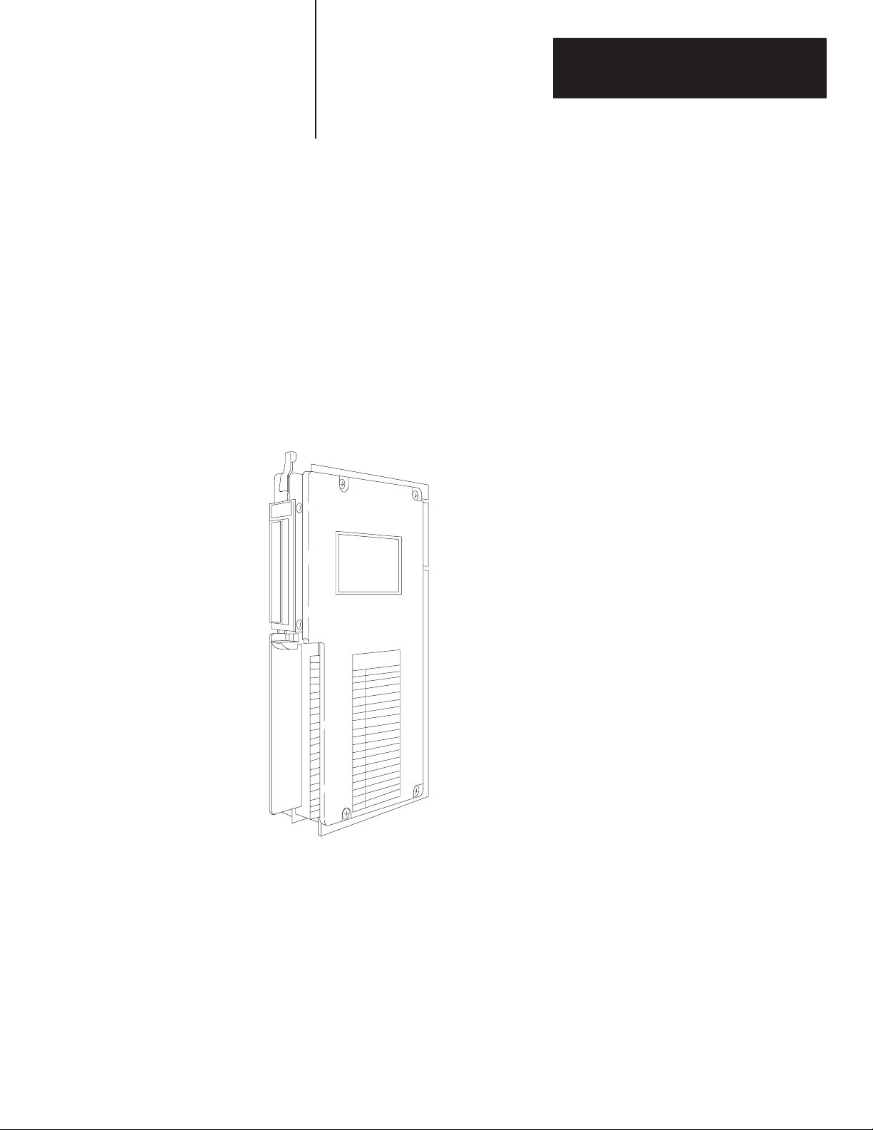
Typical Applications
In many applications, it is necessary to set or change the preset values of
timers or counters or the values of process variables. It is convenient to
do this using BCD thumbwheel switches (Figure 1.2). Applications that
require the use of multiple thumbwheel switches include, but are not
limited, to the following:
control of chemical processes
production-part adjustments used in the automatic balancing of tires
control of pallets in materials handling
cycle time adjusments in production machines and processes
Figure 1.2
Typical
3-digit Thumbwheel Switch
6
–
–
9
–
2
+
The DC (5V) Multiplexer Input Module saves I/O space and user
program. It can handle the switch input from up to six 3-digit or four
4-digit BCD thumbwheel switches. It can also handle up to 72 discrete
contact switches.
ii
+
+
17928
Page 6

T
able of Contents
WARNING: Outputs of any output module may temporarily
change operating state at power-up if placed in the same I/O
chassis with a multiplexer module, cat. no. 1771-IS, earlier
than hardware revision D, and a power supply (or processor
with self-contained power supply) other than 1771-P1 or
1771-P2. To avoid damage to equipment and/or injury to
personnel use only multiplexer modules, cat. no. 1771-IS,
hardware revision D or later.
Important: Hardware revision D is designated by part no.
XXXXXX-XX/D on the module nameplate. Earlier modules (cat. no
1771-ISC) do not have this part no./D designation.
iii
Page 7

T
able of Contents
iv
Page 8

Chapter
2
Module Preparation, Wiring and Installation
General
Switch Selection of Operating
Modes
The modes of operation must be set internally to suit the conditions under
which the module will be used. In addition, switch contacts and
decoupling diodes must be wired to the module.
The module is capable of operating in a variety of modes depending on
the kinds of switches connected to it, whether the module is placed in a
local or remote I/O rack, and/or whether latched data in module memory
will be reset automatically or by program logic after the transfer of data.
The mode selection switch is mounted near the lower rear corner of the
printed circuit board under the left side cover of the module. It is
accessible by removing the four slotted cover screws on the right side of
the module.
The modes are selected by setting the mode selection switches ON or OFF
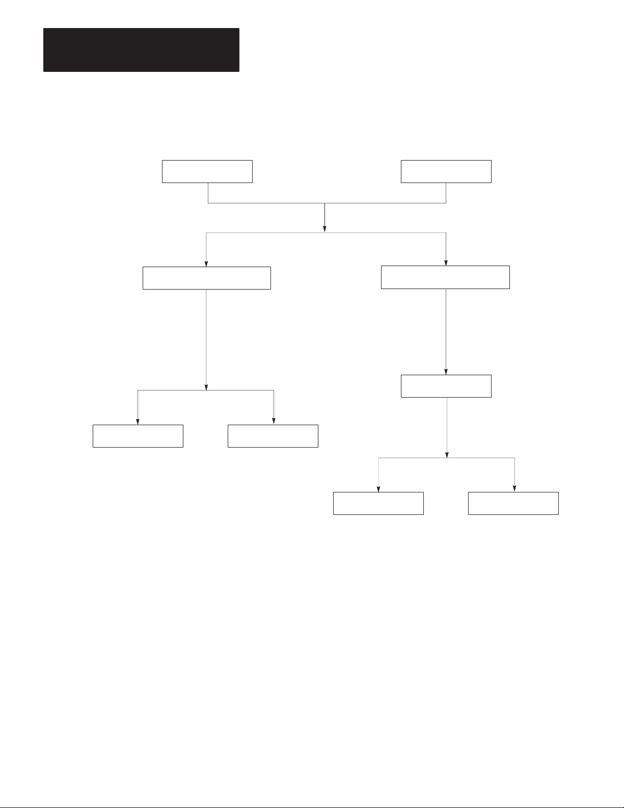
according to the positions defined in Figure 2.1.
2-1
Page 9
Chapter 2
Module Preparation, Wiring, and
Installation
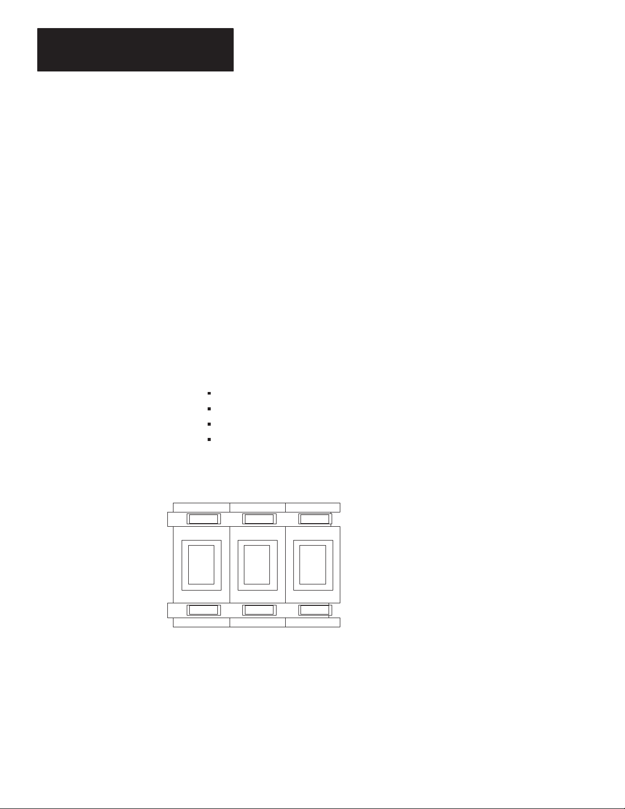
Figure 2.1
Mode
Selection Dip Switch
ON
1
OFF
ON
2
OFF
ON
3
OFF
ON Momentary (Latched) Contact Mode
4
OFF
ON
5
OFF
ON
6
OFF
ON
7
OFF
Always OFF
16–Bit Data
12–Bit Data
Fast
Normal
Maintained Contact Mode
Always OFF
Always OFF
Program Initiated Reset
Automatic Reset
1234567
O
N
O
F
F
Switch #1 - Always OFF.
Switch #2 - 16 Bit Storage/12 Bit Storage, Select 12-bit storage when
using 3-digit BCD thumbwheel switches. Select 16-bit storage when
using 4-digit BCD thumbwheel switches, discrete momentary contact
switches, or discrete maintained contact switches. (ON for 16-bit storage,
OFF for 12-bit storage.)
Switch #3 - Normal Scan/Fast Scan. The module scan is independent of
the processor scan and is generally set at the normal (15.3 msec) position.
The fast scan (5.1 msec) can be used when operating in either the
ON
OFF
ON
OFF
ON
OFF
10362
2-2
Page 10

Chapter 2
Module Preparation, Wiring and
Installation
momentary (latched) contact mode or maintained contact mode. (ON for
fast scan, OFF for normal scan.)
Switch #4 - Maintained Contact Mode/Momentary (latched) Contact
Mode. Select the maintained contact mode when storing the status, ON or
OFF, of maintained switch contacts. Their status is updated in every scan.
Select the momentary (latched) contact mode when storing momentary
OFF-ON switch contact transitions. Subsequent scans will not reset
latched bits even if the corresponding switches are reopened. The
transition is latched ON in module memory and must be reset after the
latched data is transferred to the processor. [ON for momentary (latched)
contacts, OFF for maintained contacts.] The position of SW #4 will also
affect data byte storage. See the diagrams in chapter 3 for further detail.
Switch #5 - Always OFF.
Switch # 6 - Always OFF.
Switch # 7 - Program Reset/Automatic Reset. Select program reset when
momentary (latched) switch status data is to be reset by setting a bit in a
user program instruction. Refer to section titled “Other Programming
Considerations, PLC-2 Family and PLC-3.” Select automatic reset when
momentary (latched) switch data is to be reset automatically. This switch
is not functional when the module is operating in the maintained contact
mode. (ON for program reset, OFF for automatic reset).
Important: When using momentary contact mode in remote applications,
only the program reset mode should be selected. Use program reset to
guard against loss of data during transfer to the processor. When using
momentary contact mode in local I/O applications, either the program
reset or automatic reset can be selected.
The allowable combinations of module operating modes are summarized
in Figure 2.2.
2-3
Page 11
Chapter 2
Module Preparation, Wiring, and
Installation
Figure 2.2
Allowable
Normal Scan Fast Scan
Operating Modes
1771-IS Multiplexer Module
12–Bit
Maintained Contacts
Momentary (latched) Contacts
16–Bit
16–Bit
Program Reset Automatic Reset
10363
Wiring
2-4
The wiring and programming of the module are dependent on each other.
Switch assemblies should be wired according to the wiring schematics
presented in this chapter. If wired differently, the transfer of data may not
take place or may become scrambled.
Module Wiring
Connections to the module are made through a removable field wiring
arm connector (cat. no. 1771-WF) which allows the module to be
Page 12
Chapter 2
Module Preparation, Wiring and
Installation
removed or installed in the I/O rack without disconnecting the wiring.)
The swingarm can be removed from the I/O rack at the pivot bar.
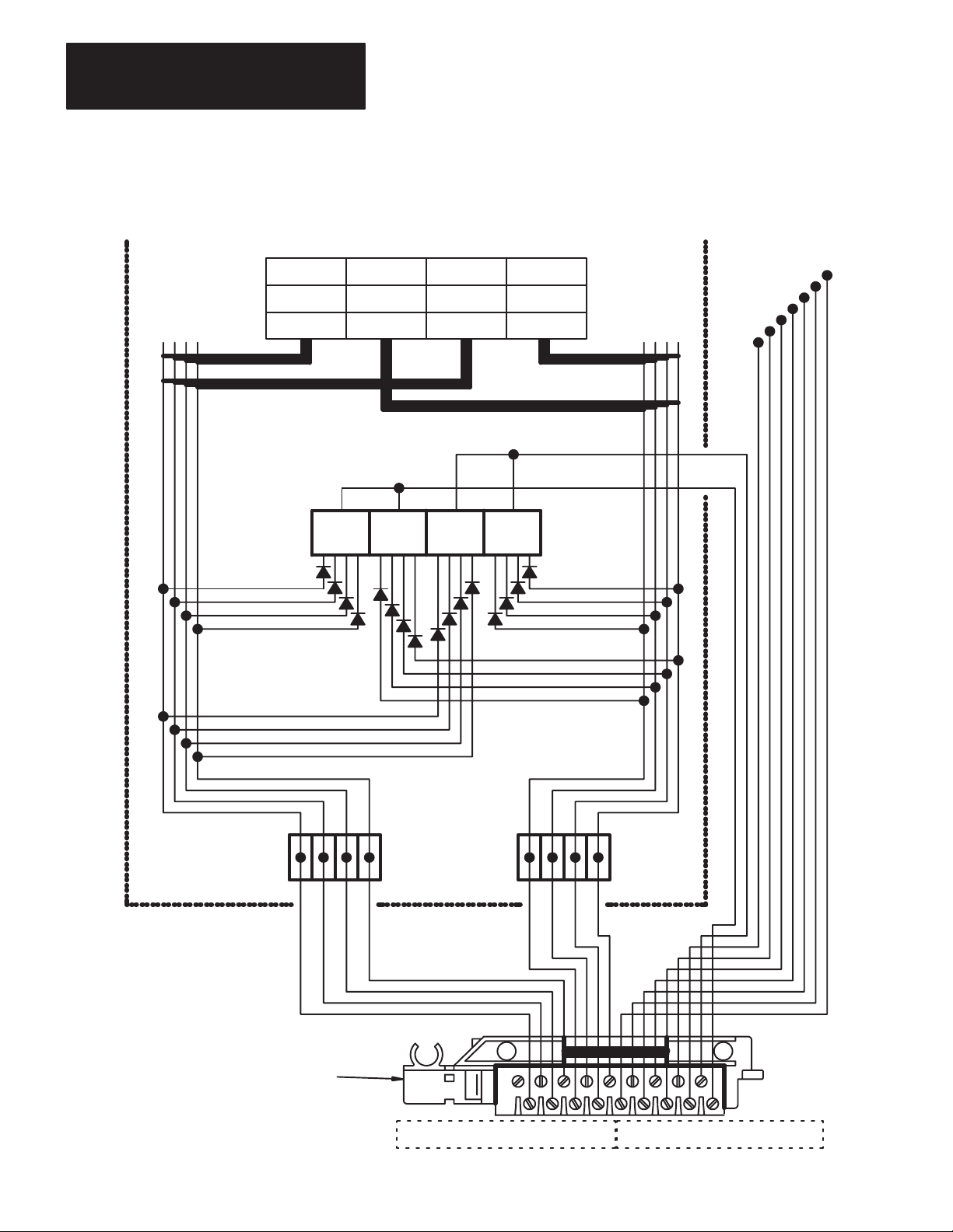
Thumbwheel Switch Wiring
Thumbwheel switch terminations are illustrated in Figure 2.3. Digit place
labels refer to the position of each digit in a 3-digit or 4-digit thumbwheel
switch as follows:
MSD and LSD - Most and Least Significant Digit; MD Middle Digit;
UMD and LMD - Upper and Lower Middle Digit, respectively.
Thumbwheel switches are wired in parallel as shown in Figure 2.4 for
4-digit switches, and in Figure 2.5 for 3-digit switches. The four switch
terminals numbered 8, 4, 2, 1 for each thumbwheel digit are wired
respectively to field wiring arm terminals 2, 3, 4, 5 or 6, 7, 8, 9. Field
wiring arm terminal 1 is not used.
4–Digit
Thumbwheel
3–Digit
Thumbwheel
Figure 2.3
Thumbwheel Terminations
Enable Lines
MSD
1
2
4
8
MSD
UMD
1
2
4
8
MD
LMD
1
2
4
8
LSD
LSD
2
4
8
Enable Lines
Digit Place Labels
Digit Place Labels
1
Switch Terminal
Numbers
1
2
4
8
4
8
1
2
4
8
1
2
Switch Terminal
Numbers
10364
2-5
Page 13
Chapter 2
Module Preparation, Wiring, and
Installation
Figure 2.4
T
ypical Point-to-point W
Switch Contact Mode)
iring for Up to Four 4-digit Thumbwheel Switches (Maintained
Enable
SW4
SW3
8421 8421
SW2
MSD UMD LMD LSD
MSD
MSD
UMD
UMD
LMD
LMD
LMD
AABB
SW1
8
421 8421 8421 8421
LSDLMDUMDMSD
LSD
LSD
4–Digit
Thumbwheel
Switch
(User Supplied)
Lines
G & H
E & F
C & D
I
H
G
F
E
D
C
B
A
2-6
8421
Field Wiring Arm
1771–WF
Digit Junction
Terminal Strip
(User Supplied)
8421
2346578
1
Module Inputs 7 6 5 4 3 2 1 0 ABCDEFGHI
9
10111213141516
18
17
Enable Lines
10365
Page 14
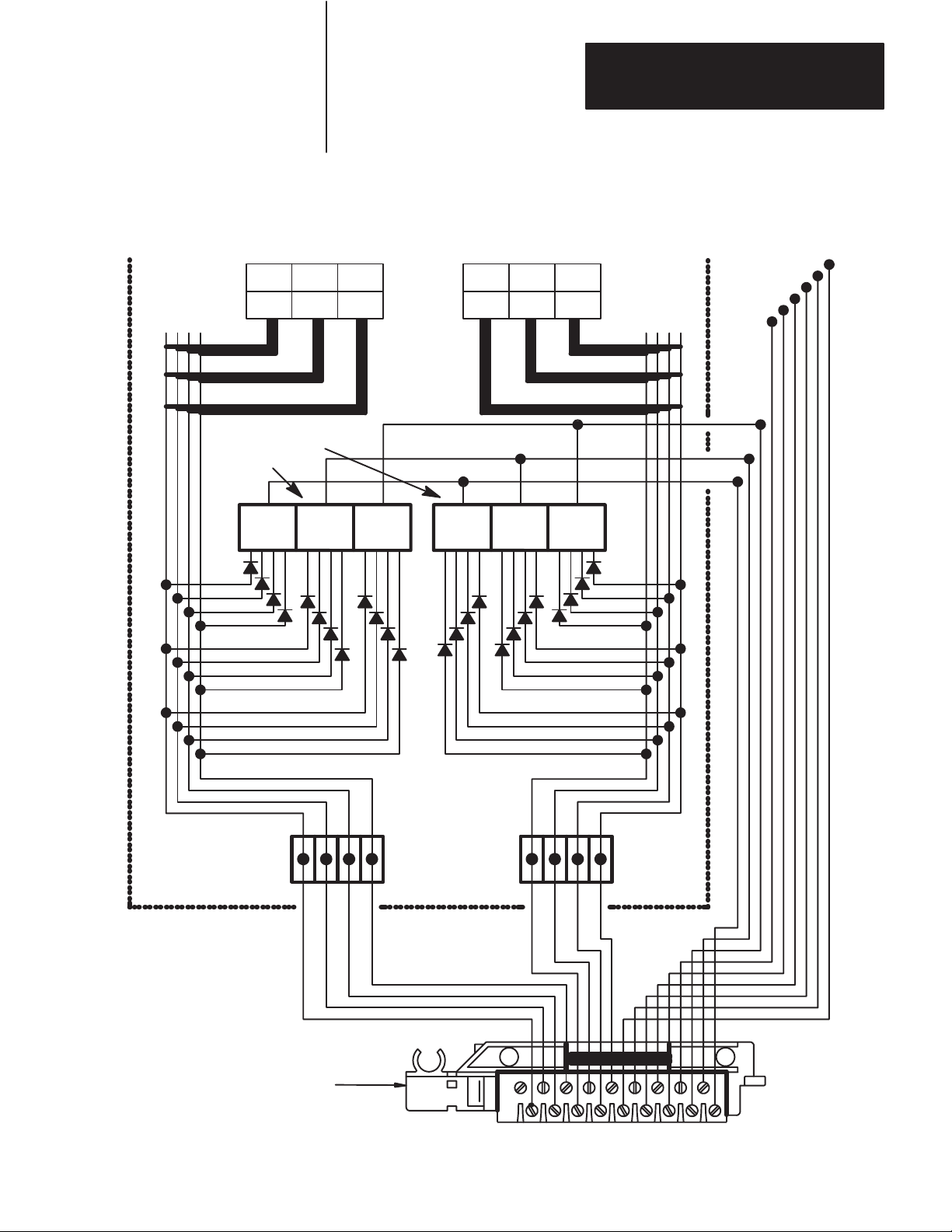
Figure 2.5
T
ypical Point-to-point W
Contact Mode)
Chapter 2
Module Preparation, Wiring and
Installation
iring for Up to Six 3-digit Thumbwheel Switches (Maintained Switch
Enable
Lines
SW6
MSD MD LSD MSD
MSD MD LSD MSD
G, H, I
D, E, F
MD LSD
MD LSD
SW3
SW2SW5
8421 8421
3–Digit
Thumbwheel Switch
(User Supplied)
SW4
ABC
MSD MD
LSD
A
MSD MD LSD
BC
SW1
8421 8421 8421 8421 8421 8421
I
H
G
F
E
D
C
B
A
8421
Field Wiring Arm
1771–WF
Digit Junction
Terminal Strip
(User Supplied)
8421
1
2345678
9
10
1112131415
Module Inputs 7 6 5 4 3 2 1 0 I H G F E D C B A
17
18
16
Enable Lines
10366
2-7
Page 15

Chapter 2
Module Preparation, Wiring, and
Installation
Important: The selection of the four field wiring arm terminals, either 2,
3, 4, 5 or 6, 7, 8, 9 is critical for correct transfer of switch status data.
The point-to-point wiring schematics show all electrical connections for
the first of several parallel switch assemblies. The wiring of additional
assemblies is shown conceptually (in the upper portion of each
schematic). Switch lines 8, 4, 2, 1 are wired to each additional switch
assembly using decoupling diodes identically to the first switch assembly.
Enable line(s) for each additional switch assembly are specified in the
conceptual part of the drawing.
The enable lines, A through I, are wired to field wiring arm terminals 18
through 10, respectively. Note that enable line A is connected to field
wiring arm terminal 18, etc. It may be desirable to terminate thumbwheel
switch lines 8, 4, 2, 1 at a terminal block on the switch panel. A single set
of switch lines 8, 4, 2, 1 and enable lines should be contained in a shielded
cable connecting the switch panel to the field wiring arm to minimize
connections at the field wiring arm terminals.
Observe the following practices when wiring thumbwheel switches:
Bundle thumbwheel switch wiring separately from other wiring.
Shielded cable is recommended.
Ground the shielded cable only at the I/O rack. The shield must remain
ungrounded at the other end.
Discrete Switch Bank Wiring
Up to 72 discrete contact switches can be wired to the module as shown in
Figure 2.6. These switches can be momentary contact or maintained
contact switches. Refer to section titled “Thumbwheel Switch Wiring”
for wiring guidelines and practices.
2-8
Page 16

Figure 2.6
Typical
Point-to-point W
Contact Mode)
Chapter 2
Module Preparation, Wiring and
Installation
iring for up to 72 Discrete Contact Switches (Maintained Switch
7 6 5 4
Bank 9
Bank 8
Bank 7
Bank 6
Bank 5
Bank 4
Bank 3
Bank 2
S7 S6 S5 S4 S3 S2 S1 S0
Discrete
Switches
(User
Supplied)
S7 S6 S5 S4 S3
S2 S1 S0Bank 1
Enable
I
H
G
F
E
D
C
B
A
Lines
3 2 1 0
I
H
G
F
E
D
C
B
A
7654
Field Wiring Arm
1771–WF
Digit Junction
Terminal Strip
(User Supplied)
Module Inputs
32 10
1
2345678
65432 0
17 I H G F E D C B A
9
10
11121314151617
18
Enable Lines
10367
2-9
Page 17

Chapter 2
Module Preparation, Wiring, and
Installation
Diode Decoupling
Decoupling diodes prevent unwanted currents from circulating through
the switch circuits and causing the false appearance of switch closures.
Use decoupling diodes when the application calls for more than 8 switch
contacts. Some thumbwheel switches have provision at the switch
terminals for wiring the diodes. Otherwise, a separate terminal strip
should be used for wiring a diode to each switch terminal. Be sure that all
diodes are wired with the same polarity as shown in Figure 2.4, Figure 2.5
or Figure 2.6.
Additional Considerations
The following information will be helpful when selecting the cable and
components, and when wiring the switches and decoupling diodes to the
module.
Low - TRUE Logic
Module operation is based on a low = TRUE logic. Enable lines, A
through I, ground the inputs connected to them through the switch
contacts. This low = TRUE condition is interpreted as a logic “1” (or
contact closed) by the module.
No External Power
The switches connected to the module are powered by the module enable
lines. Any additional power source must NOT be used.
CAUTION: Damage to the module will result if any external
power source is connected to the module field wiring arm
terminals.
2-10
Switch Selection
Any contact closure switch than can successfully handle 8 to 14mA of
current at 5V DC can be used. The minimum OFF resistance can be 10 K
ohms. The maximum ON resistance can be 10 ohms including the cable
resistance.
Page 18

Chapter 2
Module Preparation, Wiring and
Installation
CAUTION: This module is not compatible with TTL
switching. The external power source will damage the module.
When selecting BCD thumbwheel switches, be sure that they are equipped
with decoupling diodes or that terminals are available on the thumbwheel
switch so that the diodes can be wired directly to the switch assembly.
The diode polarity must be set for low = TRUE operation. Cathodes must
be connected to the switch contacts and anodes to the module inputs (lines
8, 4, 2, 1).
When selection thumbwheel switches, be sure to select a BCD type.
Decimal thumbwheel switches should be avoided because the 10 discrete
connections for each digit would not be compatible with the 4 BCD coded
input terminals for each digit on the module swingarm.
Keying
Diode Selection
Any diode can be used for diode decoupling that has a forward voltage
drop of approximately 0.7 volts at 14 mA forward current. A 1N914 is a
typical diode that can be used.
Cable Selection
The maximum cable capacitance can be .039 microfarad. The wire size
can be 20 gauge or larger for cables shorter than 100 feet; and 18 gauge
for up to 400 feet. The cable should be shielded and should not exceed
400 feet in length.
The backplane connector should be keyed to accept only this module after
its position in the I/O rack has been determined. The module can be
placed in any I/O slot except for the left-most slot. Th slot is reserved for
the processor module in a single rack system or the I/O adapter module in
a multi-rack system.
Plastic keying bands shipped with the I/O chassis should be used. The
position of the keying bands on the upper backplane connector must
correspond to the mating slots on the module connector.
2-11
Page 19

Chapter 2
Module Preparation, Wiring, and
Installation
Refer to Figure 2.7. Using needle-nose pliers, place the keying bands
between these numbers on the backplane:
Between 8 and 10
Between 26 and 28
Figure 2.7
Keying
Diagram
2
4
6
8
10
12
14
16
18
20
22
24
26
28
30
32
34
36
2
4
6
8
10
12
14
16
18
20
22
24
26
28
30
32
34
36
2
4
6
8
10
12
14
16
18
20
22
24
26
28
30
32
34
36
Keying
Bands
Backplane
Connector
17871
The position of the keying bands can be changed if subsequent system
design requires the module to be moved to a different location.
2-12
Page 20

Chapter
Programming and Operation
3
General
Module Scan of Switch Contacts
Storage of Switch Contact Data
Switch status data is stored in the module, transferred to the data table
upon request by block transfer instructions, then stored in a data table file
until operated upon by user program instructions.
The user-selectable scan rates are 15.3 msec (normal) and 5.1 msec (fast).
The nine enable lines, A through I, are sequentially and repeatedly
enabled, one line at a time. The enable lines operate in a low = TRUE
logic. Each enable line can enable a bank of 8 switches simultaneously.
The module allows for contact debouncing before the module’s
microprocessor reads the status of the switch bank. Scanning is
continuous unless interrupted by a user program instruction to transfer the
status of the switch contacts to the data table. Scanning resumes at the
same point where it was interrupted after the data is transferred.
BCD thumbwheel switches convert selected decimal numbers to a switch
status setting. Four switch contacts are required to encode each decimal
digit of a thumbwheel switch in BCD. Switch status can be transferred to
the processor data table and stored in word format by user program
instructions (Figure 3.1).
Figure 3.1
Bit
Pattern of a Thumbwheel Setting
2951
MSD UMD LMD LSD
8421842184218421
17 10 07 00
00101001
01010001
Thumbwheel settings
Digit place labels
Switch status setting
Switch terminal numbers
Bit numbers
Equivalent bit pattern
(1 data table word)
10369
3-1
Page 21

Chapter 3
Programming and Operation
4-digit Thumbwheel Switch Data (16-bit storage)
Data is loaded into memory based on whether you have selected the
maintained or momentary switch contact mode (SWITCH #4).
Maintained Contact Mode
When 4-digit BCD thumbwheel switches are wired according to the block
diagram in Figure 3.2a, the switch settings will be stored automatically in
the data table after a block transfer as shown in Figure 3.2b. The first
word is reserved for diagnostic data. Each remaining word stores the four
digits of the thumbwheel setting. The digits MSD, UMD, LMD and LSD
have been loaded, respectively, from left to right, in the same order that
they are normally read (left to right). For example, observe how the
4-digit switch setting 9753 of thumbwheel switch #2 is loaded into the
data table.
3-2
Page 22

Chapter 3
Programming and Operation
Figure 3.2
4-digit
Thumbwheel Switch Data Storage, Maintained Contacct mode ( SWITCH #4 OFF)
A
MSD UMD
LMD LSD
B
C
9 7
35
D
E
MSD UMD
LMD LSD
F
G
MSD UMD
LMD LSD
H
I
Switch 1
a) Block Diagram
User Thumbwheel
Switch 2
9 7 5 3
Switch 3
Switch 4
Switch
Terminals
Field Wiring Arm
Terminals
Data
Table
Word
XX0
1
2
3
4
5
Extra Byte
2 8
3 4
4 2
5 1
Switch Status Data
17
Diagnostics - - -
MSD UMD LMD LSD 1
97532
MSD UMD LMD LSD 3
MSD UMD LMD LSD 4
--
10 07
1/2 Switch 5
8 6
4 7
2 8
1 9
Extra Byte
Switch
Terminals
Field Wiring Arm
Switch
Number
00
5
Terminals
b) Data Table Map
10370
3-3
Page 23

Chapter 3
Programming and Operation
Momentary Contact Mode
When 4-digit BCD thumbwheel switches are wired according to the block
diagram in Figure 3.3a, the switch settings will be stored automatically in
the data table after a block transfer as shown in Figure 3.3b. The first
word is reserved for diagnostic data. Each remaining word stores the 4
digits of the thumbwheel setting. The digits MSD, UMD, LMD and LSD
have been loaded, respectively, from left to right, in the opposite byte
order from which they normally read (left to right). For example, observe
how the 4-digit switch setting 9753 of thumbwheel switch #2 is loaded
into the data table.
3-4
Page 24

Chapter 3
Programming and Operation
Figure 3.3
4-digit
Thumbwheel Switch Data Storage, Momentary Contact Mode ( SWITCH #4 ON)
A
MSD UMD
LMD LSD
B
C
9 7
35
D
E
MSD UMD
LMD LSD
F
G
MSD UMD
LMD LSD
H
I
Switch 1
a) Block Diagram
User Thumbwheel
Switch 2
9 7 5 3
Switch 3
Switch 4
Switch
Terminals
Field Wiring Arm
Terminals
Data
Table
Word
XX0
1
2
3
4
5
Extra Byte
2 8
3 4
4 2
5 1
Switch Status Data
17
Diagnostics - - -
MSD UMD LMD LSD 1
53972
MSD UMD LMD LSD 3
MSD UMD LMD LSD 4
--
10 07
1/2 Switch 5
8 6
4 7
2 8
1 9
Extra Byte
Switch
Terminals
Field Wiring Arm
Switch
Number
00
5
Terminals
b) Data Table Map
10370
3-5
Page 25

Chapter 3
Programming and Operation
Important: The 16-bit data position (switch #2 ON) should be selected
when 4-digit thumbwheel switches or discrete contact switches are used.
Otherwise switch status data from these devices can become scrambled
when transferred to the data table.
Discrete Contact Switch Data (16-Bit storage)
Data is loaded into memory on the basis of whether you have selected the
maintained or momentary switch contact mode (switch #4).
Momentary Contact Mode
When up to 72 discrete contact switches are wired as switch banks,
Figure 3.4a, the settings are stored automatically in the data table after a
block transfer as shown in Figure 3.4b. The first word is reserved for
diagnostic data. Each remaining word stores the status of two switch
banks. The settings of a switch bank are represented by S7, S6, S5, S4,
S3, S2, S1, S0.
Data of odd-numbered switch banks appears in the lower byte, and data of
even-numbered switch banks appears in the upper byte, of their respective
data table words. For example, observe how the ON/OFF settings of
switch banks 5 and 6 are loaded into the data table in Figure 3.4b.
3-6
Page 26

Figure 3.4
Discrete-Contact
Chapter 3
Programming and Operation
Switch Bank Data Storage (SW #4 ON (Momentary) Mode)
A
S7 S6 S5 S4 S3 S2 S1 S0
Bank 1
B
Same
Bank 2
C
Same
Bank 3
D
Same
E
1
0 1101010
F
2
1 1100001
Bank 4
Bank 5
Bank 6
a) Block Diagram
G
S7 S6 S5 S4 S3 S2 S1 S0
Bank 7
H
Same
Bank 8
Switch
Terminals
Field Wiring Arm
Terminals
2
3
4
5
Data
Table
Word
XX0
1
4
I
Same
Bank 9
Switch
Terminals
7
6
5
4
Switch Status Data
Bit Number
17
10 07
Diagnostics
Bank 2
2
3
Bank 4
1110 0001
2
Bank 8
5
-
3
2
1
0
- -
Bank 1
Bank 3
0110 1010
Bank 7
Bank 9
6
7
8
9
Field Wiring Arm Terminals
00
1
2
1
10371
b) Data Table Map
0110
1010 shows the settings, ON or OFF
S7, S6, S5, S4, S3, S2, S1, S0 of switch bank 5.
11
10 0001 shows the settings, ON or OFF
S7, S6, S5, S4, S3, S2, S1, S0 of switch bank 6.
, of Switches
, of Switches
3-7
Page 27

Chapter 3
Programming and Operation
Maintained Control Mode
When up to 72 discrete contact switches are wired as switch banks,
Figure 3.5a, the settings are stored automatically in the data table after a
block transfer as shown in Figure 3.5b. The first word is reserved for
diagnostic data. Each remaining word stores the status of two switch
banks. The settings of a switch bank are represented by S7, S6, S5, S4,
S3, S2, S1, S0.
Data of odd-numbered switch banks appears in the upper byte, and data of
even-numbered switch banks appears in the lower byte of their respective
data table words. For example, observe how the ON/OFF settings of
switch banks 5 and 6 are loaded into the data table in Figure 3.5b.
3-8
Page 28

Figure 3.5
Discrete-Contact
Chapter 3
Programming and Operation
Switch Bank Data Storage (SW #4 OFF (Maintained) (Mode)
A
S7 S6 S5 S4 S3 S2 S1 S0
Bank 1
B
Same
Bank 2
C
Same
Bank 3
D
Same
E
1
0 1101010
F
2
1 1100001
Bank 4
Bank 5
Bank 6
a) Block Diagram
G
S7 S6 S5 S4 S3 S2 S1 S0
Bank 7
H
Same
Bank 8
Switch
Terminals
Field Wiring Arm
Terminals
2
3
4
5
Data
Table
Word
XX0
1
4
I
Same
Bank 9
Switch
Terminals
7
6
5
4
Switch Status Data
Bit Number
17
10 07
Diagnostics
Bank 2
2
3
Bank 4
0110 1010
1
Bank 8
5
-
3
2
1
0
- -
Bank 1
Bank 3
1110 0001
Bank 7
Bank 9
6
7
8
9
Field Wiring Arm Terminals
00
1
2
2
10371
b) Data Table Map
0110
1010 shows the settings, ON or OFF
S7, S6, S5, S4, S3, S2, S1, S0 of switch bank 5.
11
10 0001 shows the settings, ON or OFF
S7, S6, S5, S4, S3, S2, S1, S0 of switch bank 6.
, of Switches
, of Switches
3-9
Page 29

Chapter 3
Programming and Operation
Important: When momentary switch contacts are used, the momentary
(latched) contact position (switch #4, ON) should be selected. Otherwise,
bits will be reset when the momentary contact switches open and data
representing OFF-to-ON transitions can be lost.
The maintained contact position (switch #4 OFF) should be selected if the
application calls for the use of up to 72 maintained contact switches.
3-digit Thumbwheel Switch Data (12-bit storage)
Data is loaded into memory on the basis of whether you have selected the
maintained or momentary switch contact mode (switch #4).
Maintained Contact Mode
When 3-digit BCD thumbwheel switches are wired according to the block
diagram in Figure 3.6a, the switch settings are stored automatically in the
data table after a block transfer as shown in Figure 3.6b. The first word is
reserved for diagnostic data. Each remaining word stores the three digits
of the thumbwheel setting. The digits MSD, MD and LSD have been
loaded, respectively, from left to right, in bits 13-00 in the same order that
they are normally read. For example, observe how the 3-digit switch
setting 642 of switch #3 is loaded into the data table (Figure 3.6b).
3-10
Page 30

Chapter 3
Programming and Operation
Figure 3.6
3-digit
Thumbwheel Switch Data Storage, Maintained Contact Mode ( SWITCH #4 OFF)
Switch 4
Switch 5
Switch 6
A
B
C
D
E
F
G
H
I
MSD
MD
LSD
MSD
MD
LSD
MSD
MD
LSD
MSD
MD
LSD
MSD
MD
LSD
6
4
2
A
B
Switch 1
C
D
E
F
G
H
I
Switch 2
User Thumbwheel
Switch 3
6 4 2
a) Block Diagram
Switch
Terminals
Field Wiring Arm
Terminals
Data
Table
Word
XX0
1
2
3
4
5
6
17
2
8
3
4
4
2
1
5
Diagnostics
-
-
-
-
-
-
Switch Status Data
10 07
MSD
MSD
6
MSD
MSD
MSD
MD
MD
MD
MD
MD
Switch
Field Wiring Arm
Terminals
00
-
Terminals
Switch
Number
1
2
3
4
5
6
b) Data Table Map
10372
8
6
4
7
2
8
1
9
LSD
LSD
4
2
LSD
LSD
LSD
3-11
Page 31

Chapter 3
Programming and Operation
Momentary Contact Mode
When 3-digit BCD thumbwheel switches are wired according to the block
diagram in Figure 3.7a, the switch settings are stored automatically in the
data table after a block transfer, as shown in Figure 3.7b. The first word
is reserved for diagnostic data. The remaining words store the three digits
of the thumbwheel setting. The digits MSD, MD and LSD have been
loaded in the order are shown in Figure 3.7. For example, observe how
the 3-digit switch setting 642 of switch #3 is loaded into the data table
(Figure 3.7b).
3-12
Page 32

Chapter 3
Programming and Operation
Figure 3.7
3-digit
Thumbwheel Switch Data Storage,Momentary Contact Mode ( SWITCH #4 ON)
Switch 4
Switch 5
Switch 6
A-4
B-4
C-4
D-5
E-5
F-5
G-6
H-6
I-6
MSD
MD
LSD
MSD
MD
LSD
MSD
MD
LSD
MSD
MD
LSD
MSD
MD
LSD
6
4
2
A-1
B-1
Switch 1
C-1
D-2
E-2
Switch 2
F-2
G-3
User Thumbwheel
H-3
Switch 3
642
I-3
a) Block Diagram
Switch
Terminals
Field Wiring Arm
Terminals
Data
Table
Word
XX0
1
2
3
4
5
6
17
2
8
3
4
4
2
1
5
Diagnostics
B-4
D-5
F-5
H-6
-
-
Switch Status Data
10 07
MD
B-1
D-2
F-2
MD
4
-
-
A-4
C-4
E-5
G-6
-
Switch
8
4
2
1
6
7
8
9
Terminals
Field Wiring Arm
Terminals
00
A-1
C-1
-
MSD
LSD
b) Data Table Map
E-2
MSD
6
I-6
LSD
2
-
10372A
3-13
Page 33

Chapter 3
Programming and Operation
Important: The 12-bit data position (switch #2 OFF) should be selected
when 3-digit thumbwheel switches are used. Otherwise switch status data
from this device can become scrambled when transferred to the data table.
Block Transfer of Switch Data
Switch status data can be transferred to the PC processor data table by
using block transfer instructions.
The Mini-PLC-2/15, PLC-2/30 and PLC-3 programmable controllers use
block transfer instructions. The Mini-PLC-2 (1772-LN3 Processor) and
PLC-2/20 use multiple GET instructions for programming block transfer.
Block Transfer Programming, PLC-2 Family
The processor transfers switch status data from the module to the data
table by a block transfer read operation. The following information must
be specified in order to program block transfer, whether using block
transfer instructions or multiple GET instructions. Values entered in
parentheses correspond to the programming example in paragraph titled
“Programming Example, PLC-2 Family” and Figure 3.8.
a) block length: the number of words to be transferred can be 0-7
depending on the number of switch assemblies. (03)
b) module address: rack, module group and slot number. (121)
3-14
c) data address: contains the module address in binary coded decimal
and is the first available address in the timer/counter accumulated area
of the data table. (030)
d) file address: defines the first of a group of words in the data table to
receive the transferred data and is located 100
above the data address.
8
(060)
For additional information on programming block transfer instructions,
refer to paragraph titled “Programming Considerations, PLC-2 Family”
and the Programming and Operations manual for the processor being
used.
Page 34

Figure 3.8
Example
Chapter 3
Programming and Operation
Block Transfer Programming, PLC-2 Family
Output
Image
Table
Accumulated
Area
Input
Image
Table
Preset
Area
R
Block length code
1
Diagnostics
9
8
R
1
010
Data Table
012
017
027
121
–
7
6
060
5
4
1
2
030
060
062
110
112
117
130
Output Image Table
Byte, contains Read
Enable Bit and Block
Length in binary code.
Data Address, contains
Module Address in BCD
First address, destination of
Transferred Data
Input Image Table Byte,
contains Done Bit
Storage location, contains
file address in BCD
Block Transfer Instruction
113
Rung 1
Multiple Get Instructions
11302030
Rung 1
Rung 2
Rung 3
02
G
121
130
060
R = Bit 17 = READ
012
BLOCK XFER READ
DATA ADDR:
MODULE ADDR:
BLOCK LENGTH:
FILE:
G
030
121
060–062
03
EN
17
112
DN
17
012
17
012
10
012
11
10373
3-15
Page 35

Chapter 3
Programming and Operation
Programming Example, PLC-2 Family
Two methods of programming are described: one using block transfer
instructions, the other using multiple GET instructions. Refer to
Figure 3.8. The data table mapping is the same for both.
For this example, 3 words of data are used to transfer the settings of two
4-digit thumbwheel switches. The settings are 9751 and 8642 for
thumbwheel switch assembly 1 and 2, respectively. (The first word is
reserved for diagnostic data.) The module is located in the upper slot of
rack 1 module group 2. The module address is 121
lower slot, the module address would be 120
and output bits 10, 11, 12,
8
. If located in the
8
16 and 17 used in the example would become 00, 01, 02, 06 and 07,
respectively.
Block Transfer Instructions
Rung 1 - When this rung is enabled, the switch status data in module
memory is transferred to the data table. The 3 words specified by the
block length will contain diagnostic data and the data of thumbwheel
switch assemblies 1 and 2.
The block length is set to 1 plus the number of thumbwheel switch
assemblies, or 1 plus the number of pairs of switch banks required by the
application.
Multiple Get Instructions
Read the description for BLOCK TRANSFER INSTRUCTIONS first.
Rung 1 - This rung is used to identify the module (module address 121
8
in the first GET instruction) and the first address of the destination of the
transferred data (word address 060
in the second GET instruction). The
8
rung also sets the block transfer read bit (bit 17) in the module’s output
image table byte.
3-16
Rungs 2, 3 - These rungs set the number of words to be transferred by
setting a binary bit pattern in the module’s output image table byte. Bits
10 and 11 are set ON. the binary bit pattern 11 is equivalent to the
number 3.
Page 36

Chapter 3
Programming and Operation
Programming Considerations, PLC-2 Family
The block transfer data address is the address that identifies the block
transfer instruction. Care should be taken when assigning these addresses
in the data table.
Date Address (PLC-2 Family)
The data address for a block transfer instruction should be the first
available address in the timer/counter accumulated area of the data table.
This address is 030
for the Mini-PLC-2 or -2/15. For the PLC -2/20 or
8
-2/30, this address depends on the number of I/O racks connected to the
processor module, i.e. address 020
070
for 6 racks and 2008 for 7 racks. When more than one block transfer
8
for 1 I/O rack, 0308 for 2 racks, etc. to
8
module is used, the data addresses should be consecutive.
Data Address Boundary (PLC-2 Family)
A boundary word containing zeros should be entered in the data table
following the last block transfer data address. When the processor sees
the boundary word, it terminates the block transfer search routine so that
subsequent data table values are not interpreted as the rack, module group
and slot numbers associated with block transfer data addresses.
Block Transfer Programming, PLC-3
The processor transfers switch status data from the module to the data
table by a block transfer read operation. The following information must
be specified in order to program block transfer with the PLC-3 processor.
Values entered in parentheses correspond to the programming example in
paragraph titled “Programming Example PLC-3” and Figure 3.9.
3-17
Page 37

Chapter 3
ЙЙЙЙЙ
Programming and Operation
Data T
able Maps
a) Control File (FB001:0010)
17 16 15 14 13 12 11 10 07 06 05 04 03 02 01 00
RQ EN DN ER LE SD SE RQ EN DN ER LE SD SE
0010
0011
0012
0013
0014
Figure 3.9
Example
Read Bits Write Bits
Block Transfer Programming, PLC-3
Mod. GroupRack Number
Data Table Section
File Number
Word Number
Bit Control Word (WB001:0010)
I/O Module Address
SL
Data File Address (Write)
0015
0016
0017
0018
0019
b) Data File (FD002:0012)
Data File
Addr
(FD002:0012
Bit Legend
RQ = Request
EN = Enable
DN = Done
ER = Error
WB001:0010
15
Write Data File Length
Data Table Section
File Number
Word Number
Read Data File Length
17 10 07 00
Diagnostics
9
8
LE = Latched Enable
SD = Scanner Done
SE = Scanner Error
SL = Slot Number
7
6
5
4
(Decimal 7)
1
2
Prefix Legend
F = File Address
W = Word Address
B = Binary File
D = Decimal FIle
(002)
Data File Address (Read)
(0012)
(3)
0012
0013
0014
BTR
BLOCK XFER READ
RACK:
GROUP:
MODULE:
DATA:
LENGTH =
CNTL:
001
1=HIGH
FD002:0012
FB001:0010
CNTL
EN
12
CNTL
2
DN
15
CNTL
3
ER
13
3-18
10374
Page 38

Chapter 3
Programming and Operation
length: the number of words to be transferred can be 0-7 depending on
the number of switch assemblies. (03)
module address: rack, module group and slot number where 1 =
HIGH = upper slot, 0 = LOW = lower slot. (121)
control file address: location of a 10-word file necessary for block
transfer read and write operations, contains the module address in
binary, the address of the data file and the block transfer status/control
bits. (FB002:0010)
data file address: location of the source or destination of block
transfer data, generally equal in length to the maximum number of
transfer words. (FD002:0012)
For additional information on programming block transfer instructions,
refer to paragraph titled “Other Programming Considerations, PLC-2
Family and PLC-3” and the Programming and Operation Manual for the
PLC-3 processor.
Programming Example, PLC-3
To program block transfer with a PLC-3 processor, you must create a
control file and a data file (Figure 3.9). The control file can be located
anywhere in the binary section of the processor data table. The data file
for thumbwheel switches should be entered in the decimal section of the
processor data table; the data file for discrete switches in the binary
section of the processor data table. Neither block transfer file should
overlap other assigned storage words.
This example is similar to the one described in paragraph titled
“Programming Example, PLC-2 Family,” except that the rung is
programmed for recurring block transfers. Three words of data are used
to transfer the settings of two 4-digit thumbwheel switches. The settings
are 9751 and 8642 for thumbwheel switch assemblies 1 and 2,
respectively. (The first word is reserved for diagnostic data.) The module
is located in the upper slot of module group 2 in I/O rack 1. The
explanation of the single programming rung is that described for block
format instructions in paragraph titled “Programming Example, PLC-2
Family.”
3-19
Page 39

Chapter 3
Programming and Operation
Other Programming Considerations, PLC-2 Family and PLC-3
When programming block transfer instructions the following should also
be considered.
Automatic/Program Reset, switch #7
When in momentary (latched) contact mode, latched data should be reset
after its image is transferred to the data table. It can be reset by program
logic (program reset mode) or automatically by the module (automatic
reset mode).
In program reset mode, module memory can be reset by user program
after a successful transfer has occurred by setting bit 6 or 16 in the
module’s output image table byte. (Bit 6 is set when the module is in the
lower slot, bit 16 when in the upper slot.) If bit 6 or 16 is set by mistake
during a request for block transfer, the module will respond that it is not
ready to transfer.
Important: Bit 6 or 16 should be programmed only when mode selection
switch #4 and #7 are both in the ON position. Refer to paragraph titled “
Switch Selection of Operating Modes” (Chapter 2).
Reset rungs are illustrated for the PLC-2 family and PLC-3 programmable
controllers in Figure 3.10. The reset condition can be conditioned upon
the completion of a successful block transfer. The output energize
instruction sets the reset bit of the module.
In program reset mode, if any bit in addition to bit 6 or 16 is on, the
module will not reset.
3-20
Page 40

Block Transfer, PLC-2 Family
Optional
Condition
Reset
Condition
Reset
Condition
Multiple GET, PLC–2 Family
Optional
Condition
Reset
Condition
Reset
Condition
Reset
Condition
Store
Word
G
000
Reset
Condition
Store
Word
G
000
030
G
121
Figure 3.10
Examples
030
G
060
of Program Reset
Chapter 3
Programming and Operation
BLOCK XFER READ
DATA
ADDR:
MODULE ADDR:
BLOCK LENGTH:
FILE
Use bit 6 if module is in the left slot of
module group.
060 – 062
030
121
03
012
EN
17
112
DN
17
012
PUT
012
16
012
17
012
10
012
11
012
PUT
012
PLC–3 Block Transfer
Optional
Condition
Reset
I0010
00
NOTES:
a) Module is located in rack 1, module group 2, slot 1
b) If any bit in addition to bit 6 or 16 is set in the store word, the module will not reset.
WB001:0010
15
Reset
I
0010
00
Use bit 6 if module is in the left slot of
module group.
BTR
BLOCK XFER READ
RACK :
GROUP
:
MODULE:
DATA:
LENGTH:
CNTL:
Use bit 6 if module is in the left slot of
module group.
1 = HIGH
FD002:0012
FB001:0010
001
16
CNTL
EN
12
CNTL
2
DN
15
3
CNTL
ER
13
O0012
16
3-21
Page 41

Chapter 3
Programming and Operation
In automatic reset mode, the module resets its data and stores new latched
data after each block transfer. Allow at least 20ms between block
transfers for the module to store new data. A method for doing this is
shown in Figure 3.11.
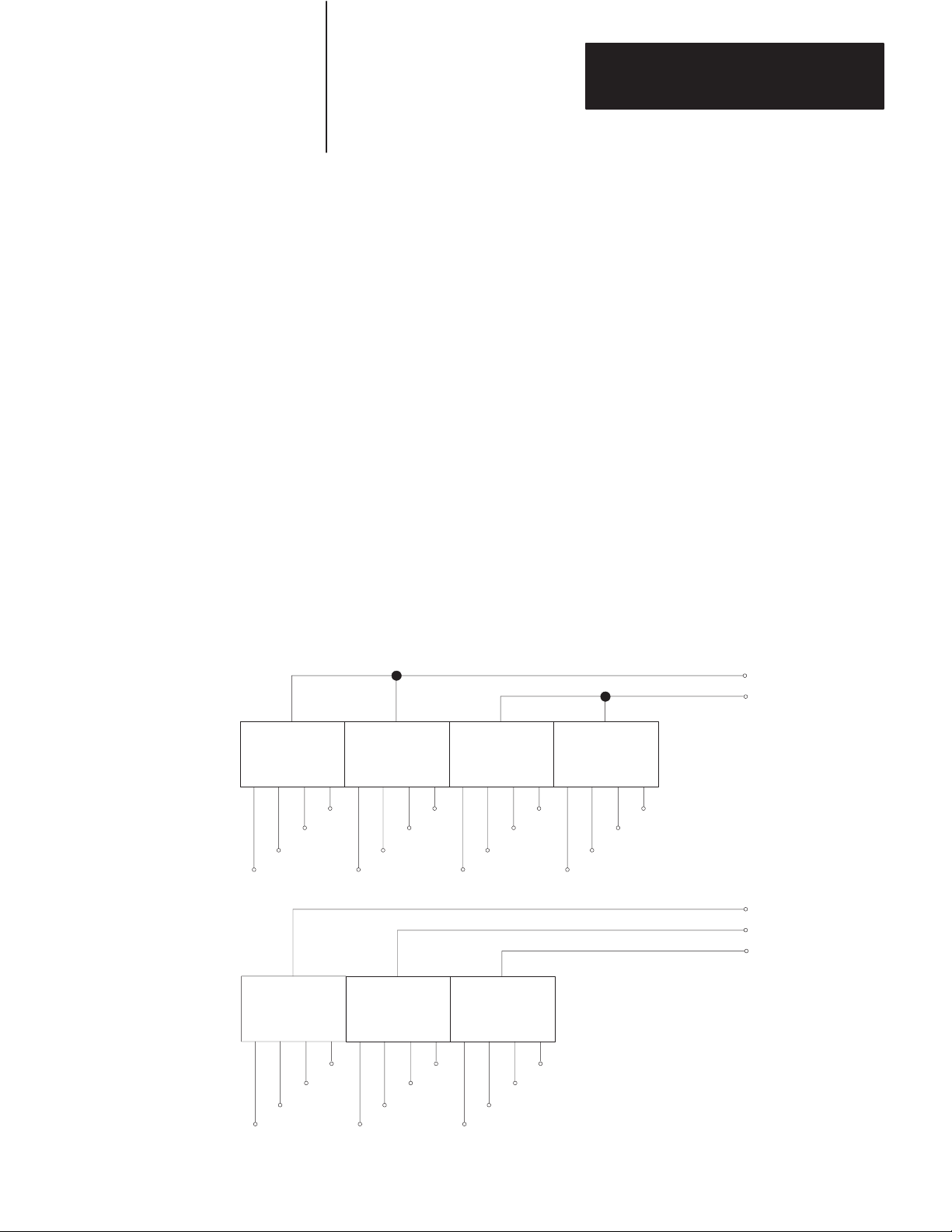
Figure 3.1
Example
Block Transfer in a Local AND a Remote System – PLC –2 Family
111
17
070
15
071
00
070
/
15
Multiple GET, PLC–2 Family
050
/
15
1
Logic for Automatic Reset, Latched Contacts Mode
BLOCK XFER READ
DATA
ADDR:
MODULE ADDR:
BLOCK LENGTH:
FILE
200 – 277
050
111
00
071
U
ON 00
071
L
ON 00
011
EN
17
111
DN
17
070
TON
.01
PR 002
AC 000
050
TON
.01
PR 002
AC 000
3-22
050
15
Optional
Condition
030
G
121
030
G
060
012
17
012
10
012
11
Page 42

PLC–3 Block Transfer
B001:0010
15
T0001
15
BLOCK XFER DONE
TIMER DONE
Chapter 3
Programming and Operation
B002:0000
U
00
B002:0000
L
00
B002:0000
00
T0001
/
NOTES:
a) Module located in rack 1, module group 2, slot 1.
b) Timer allows at least 20ms between block transfers.
Diagnostics
BTR
BLOCK XFER READ
RACK :
:
GROUP
MODULE:
DATA:
LENGTH:
CNTL:
TON
TIMER ON T0001
0.01 SECOND
TP = 2
TA = 0
1 = HIGH
FD002:0012
FB001:0010
001
CNTL
EN
12
CNTL
2
DN
15
3
CNTL
ER
13
T0001
TE
17
T0001
TD
15
Bit 12 of the block transfer diagnostic word is the communication fault
bit. A communication fault can be caused either by cycling power to the
processor, by a break in I/O communications or by excessive electrical
noise radiating into the I/O communication cable. This bit will go ON if
the transfer is aborted. The I/O communication cable and system
grounding should be checked thoroughly in accordance with grounding
and shielding recommendations presented in the processor Assembly and
Installation Manual. This bit can be reset only by cycling power to the
module.
Data Buffering
Data that is block transferred to the data table should be buffered before it
is used to guard against the manipulation of invalid data by subsequent
user program instructions.
3-23
Page 43

Chapter 3
Programming and Operation
This can be done by examining the block transfer done bit for an ON
condition. An EXAMINE ON instruction addressed to the done bit
should be a logic condition for any further manipulation of transferred
data. The done bit for the PLC-2 family and PLC-3 programming
example is 112/17 and WB001:0010/15, respectively.
WARNING: Program the examination of the block transfer
done bit as a condition for subsequent data manipulation
following each block transfer. Otherwise, invalid data could be
operated upon causing unexpected machine operation with
possible damage to equipment and/or injury to personnel.
The communication fault bit, bit 12 of the diagnostic word, can be
examined as an additional buffering condition. This can be done by using
an EXAMINE OFF instruction addressed to bit 12 of the diagnostic
word’s location in the data table (060/12 for PLC-2 family,
WD002:0012/12 for PLC-3 in this example). If transfer was aborted, the
next transfer of data would contain bit 12 ON, in the diagnostic word.
3-24
Page 44

Specifications
Module
Inputs
Up to four 4–digit BCD
Thumbwheel Switches or
Appendix
A
Module Current Requirement
800 mA max @ 5V DC from
the backplane
Up to six 3–digit BCD
Thumbwheel Switches or
Up to 72 Discrete Contact
Switches (Maintained or
Momentary contact)
Diode Decoupling is required
for more than 8 Switch
Contacts
Module Location
Any Bulletin 1771 I/O Rack
location except the left–most
slot
Switch Power Requirement
Supplied by the module
Nominal 13 mA @ 5V DC
per switch
Maximum Switch Cable Distance
400 feet
Ambient T
Humidity
Keying
emperature Rating
0–60 0C Operational
–20 to +850 C Storage
5% to 95%
(without condensation)
Keying positions are between
8 and 10 and between 26 and
28
i
Page 45

T
able of Contents
ii
Page 46

Index
I
Symbols
**Empty**, 2-1
1 , 3-19
Numbers
4–digit thumbwheel switch data, 3-2
A
automatic, 3-22
D
Data buf
data storage, 3-6
Decoupling, 2-10
fering, 3-23
Diagnostics, 3-23
Dip switch settings, 2-1
Discrete contact switch data, 3-6
Discrete switch bank wiring, 2-8
E
external power
, 2-10
K
Keying, 2-1
1
L
Low = TRUE, 2-10
I–1
Page 47

I
M
Mode selection dip switch, 2-1
Module scan of switch contacts, 3-1
Module wiring, 2-4
O
od switch data, 3-14
P
PLC–2 family
, 3-14
R
reset, 3-20
Index
S
selection, 2-1
Specifications, A-1
1
T
Thumbwheel switch wiring, 2-5
T
ypical Applications, 1-2
W
When to use 16–bit or 12–bit storage, 2-2
Wiring, 2-4
with 3–digit thumbwheel switch data, 3-10
–2 I–2
Page 48

 Loading...