

Page 1

Installation Instructions
Analog Input Module
(Catalog Number 1771-IFE/C)
Contents
This
icon is used when
additional information
is available in the
Input Module User Manual
publication 17716.5.1
If you need a copy of this
manual, fax the enclosed
User Manual Request Card
to 18005766340. If you
are outside the U.S., fax the
card to13307234036.
Analog
15.
Use this document as a guide when installing the 1771-IFE/C analog
input module.
To See page
Prevent Electrostatic Discharge Below
Understand Compliance to European Union Directives 2
,
Understand Product Compatibility 2
Calculate Power Requirements 3
Determine Module Placement 3
Set the A/B Simulation Jumper 3
Set the Configuration Jumpers 4
Key the Backplane Connector 4
Install the Module and Field Wiring Arm 5
Connect Wiring to the Field Wiring Arm 6
Ground the Chassis and Module 9
Configure the Module 10
For this reference information See page
Status Indicators 12
Troubleshooting 13
Specifications 13
CSA Hazardous Approval 15
Differences Between Series A, B and C Modules 16
Prevent Electrostatic Discharge
The analog input module is sensitive to electrostatic discharge.
ATTENTION: Electrostatic discharge can damage
integrated circuits or semiconductors if you touch
!
backplane connector pins. Follow these guidelines
when you handle the module:
• Touch a grounded object to discharge static potential
• Wear an approved wrist-strap grounding device
• Do not touch the backplane connector or
connector pins
• Do not touch circuit components inside the module
• If available, use a static-safe work station
• When not in use, keep the module in its
static-shield box
Publication 17715.45 - July 1997
Page 2
Analog Input Module2
Number
Image
Image
Block
Block
Chassis
Understand Compliance to European Union Directives
If this product has the CE mark it is approved for installation within
the European Union and EEA regions. It has been designed and
tested to meet the following directives.
EMC Directive
This product is tested to meet Council Directive 89/336/EEC
Electromagnetic Compatibility (EMC) and the following standards,
in whole or in part, documented in a technical construction file:
• EN 50081-2EMC – Generic Emission Standard,
Part 2 – Industrial Environment
• EN 50082-2EMC – Generic Immunity Standard,
Part 2 – Industrial Environment
This product is intended for use in an industrial environment.
Low Voltage Directive
This product is tested to meet Council Directive 73/23/EEC
Low Voltage, by applying the safety requirements of EN 61131–2
Programmable Controllers, Part 2 – Equipment Requirements and
Tests.
Understand Product Compatibility
For specific information required by EN 61131-2, see the appropriate
sections in this publication, as well as these Allen-Bradley
publications:
Publication Publication number
Industrial Automation Wiring and Grounding Guidelines
For Noise Immunity
Guidelines for Handling Lithium Batteries AG5.4
Automation Systems Catalog B111
17704.1
The 1771-IFE module can be used with any 1771 I/O chassis.
Compatibility and data table use is listed below.
Use of Data Table Compatibility
Catalog
Number
1771IFE 8 8 22 39 Y Y Y A, B
A
= Compatible with 1771A1, A2, A4
B = Compatible with 1771A1B, A2B, A3B, A3B1, A4B
Y = Compatible without restriction.
Input
Ima
Bits
Output
e
Ima
Bits
Read
e
Block
Words
Write
Block
Words
Addressing
1/2Slot 1Slot 2Slot
Chassis
Series
Do not use this module with cat. no. 1771-AL PLC-2/20 or 2/30
Local Adapter.
Publication
17715.45 - July 1997
Page 3
Analog Input Module 3
Calculate Power Requirements
Determine Module Placement in the I/O Chassis
The module receives its power through the 1771 I/O power supply
and requires 500mA from the backplane.
Add this current to the requirements of all other modules in the I/O
chassis to prevent overloading the chassis backplane and/or
backplane power supply.
Place your module in any I/O module slot of the I/O chassis except
for the extreme left slot. This slot is reserved for PC processors or
adapter modules.
ATTENTION: Do not insert or remove modules from
the I/O chassis while system power is ON. Failure to
!
observe this rule could result in damage to module
circuitry.
Group your modules to minimize adverse affects from radiated
electrical noise and heat. We recommend the following.
• Group analog input and low voltage dc modules away from ac
modules or high voltage dc modules to minimize electrical noise
interference.
• Do not place this module in the same I/O group with a discrete
high-density I/O module when using 2-slot addressing. This
module uses a byte in both the input and output image tables for
block transfer.
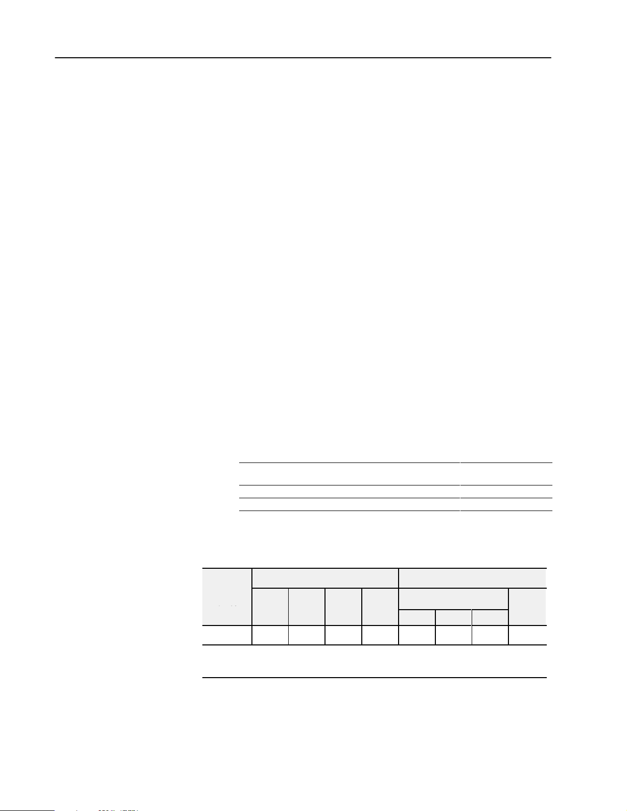
Set the A/B Simulation Jumper
The module is shipped with the A/B simulation jumper set in
position POS G for Series C applications. This setting returns input
data above and below the range end points. If you are replacing a
Series A or B 1771-IFE module with this module, reset the
simulation jumper to the POS E position as shown below.
Set the Series A/B Simulation Jumper
1. Locate the simulation jumper at the top edge
of the module circuit board.
2. Using your fingers, slide the jumper off the 2 posts.
3. Carefully position the jumper on 2 of the 3 posts that
correspond to your requirement.
A/B
Simulation Jumper
Series
A and B
Simulation
Series C
Application
Top edge of circuit board
POS G POS E
Simulation Jumper (shown in A/B position)
Top edge of circuit board
POS G POS E
Simulation Jumper (shown in series C position)
Publication
17715.45 - July 1997
Page 4
Analog Input Module4
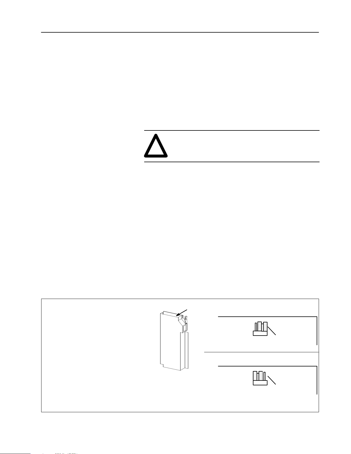
Set the Configuration Jumpers and Key the Backplane Connector
Remove the four screws securing the side cover to
11
the module and remove the covers.
Reposition the cover and secure with the four
13
screws removed in step 1.
19813
The module has configuration jumpers for determining the input type
(voltage or current) desired for each input. The module is shipped
with the configuration jumpers positioned for voltage mode and
the A/B simulation jumper set for Series C. If you are replacing a
Series A or B 1771-IFE module with this module, reset the
simulation jumper as shown above.
You can select either voltage or current for each input, but all inputs
must be either single-ended or differential. Do not mix single-ended
and differential inputs on the module.
Reposition the configuration jumpers associated with each input
12
channel according to your requirements
You can mix voltage mode and current mode settings on
the module. Make sure that the entire module is set for
either singleended or differential. Do not mix them.
Voltage Mode
Differential or Singleended (factory set)
DifferentialSingleended
Channel 1
Channel 2
Channel 3
Channel 4
Channel 5
Channel 6
Channel 7
Channel 8
19805
Current Mode
Differential
Current
Singleended
Odd channel current
Even channel voltage
Even channel current
Odd channel voltage
Singleended
Current
Channel
1 and 2
Channel
3 and 4
Channel
5 and 6
Channel
7 and 8
Channel
9 and 10
Channel
1 and 12
1
Channel
13 and 14
Channel
15 and 16
Configuration
Jumpers
4
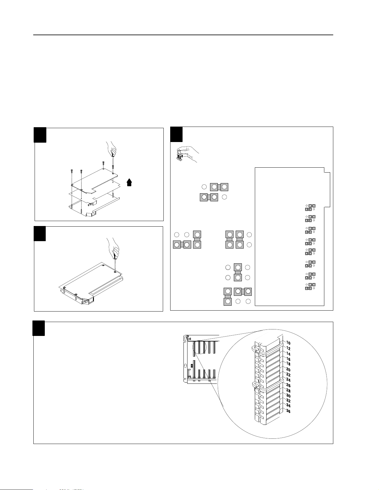
Key the Backplane Connector
Place your module in any slot in the chassis
except the leftmost slot which is reserved for
processors or adapters.
Position the keying bands in the backplane connectors
to correspond to the key slots on the module.
Place the keying bands:
between 10 and 12
between 24 and 26
You can change the position of these bands if
subsequent system design and rewiring makes
insertion of a different type of module necessary.
Publication
17715.45 - July 1997
I/O chassis
Upper Connector
11022I
Page 5

Analog Input Module 5
Install the Module and Field Wiring Arm
!
ATTENTION: Remove power from the 1771 I/O
chassis backplane and field wiring arm before
removing or installing an I/O module.
• Failure to remove power from the backplane or
wiring arm could cause module damage, degradation
of performance, or injury.
• Failure to remove power from the backplane could
cause injury or equipment damage due to possible
unexpected operation.
Place the module in the card guides on the top and bottom of the chassis that guide the module into position.
1
1
Important: Apply firm even pressure on the module to seat it into its
backplane connector.
1771A1B, A2B, A3B1, A4B Series B I/O chassis1771A1B, A2B, A3B, A3B1, A4B I/O chassis
Snap the chassis latch over the
top of the module to secure it.
Swing the chassis locking bar
down into place to secure the
modules. Make sure the locking
pins engage.
2
Attach the wiring arm (1771WG) to the horizontal
bar at the bottom of the I/O chassis.
The wiring arm pivots upward and connects with
the module so you can install or remove the
module without disconnecting the wires.
horizontal bar
remove
install
wiring arm
1771WG
17643
Publication
17715.45 - July 1997
Page 6

Analog Input Module6
Connect Wiring to the Field Wiring Arm
Connect your I/O devices to the cat. no. 1771-WG wiring arm
shipped with the module.
ATTENTION: Remove power from the 1771 I/O
chassis backplane and field wiring arm before
!
removing or installing an I/O module.
• Failure to remove power from the backplane or
wiring arm could cause module damage, degradation
of performance, or injury.
• Failure to remove power from the backplane could
cause injury or equipment damage due to possible
unexpected operation.
Input connections for the 1771-IFE module with:
• single-ended inputs are shown on page 7
• differential inputs are shown on page 8
Minimizing Ground Loops
To minimize ground-loop currents on input circuits:
• use single-ended mode whenever possible
• use 2-wire transmitters with a common power supply
• separate 2-wire and 4-wire transmitters between different
modules
• tie 4-wire transmitter and/or separate power supply grounds
together
Important: We do not recommend mixing 2-wire and 4-wire
transmitter inputs on the same module. Power supply
placement can make it impossible to eliminate ground
loops.
Cable Lengths
Recommended maximum cable length for voltage-mode input
devices is 50 feet. This recommendation is based on considerations
of signal degradation and electrical noise immunity in typical
industrial environments. Cable length for current-mode input
devices need not be as restrictive because analog signals from these
devices are less sensitive to electrical noise interference.
Publication
17715.45 - July 1997
Page 7

Analog Input Module 7
Connection
Note:
specifications for power supply connections.
NOTE:
- All module commons are electrical
ly tied together inside the module.
- Jumper all unused channels to module
common to reduce noise.
- T
ie power supply grounds together to
minimize ground loops.
Attention: Analog input signals must be within +
to module common. This input signal includes any common mode
voltage present between either input terminal and module common.
If an input terminal exceeds this range, channeltochannel
crosstalk can cause invalid input readings and invalid underrange
or overrange bits.
The 1771IFE module does not supply loop power for the input device.
The user must supply loop power for looppowered input devices.
Diagram for 16 Singleended Inputs and T
Refer to transmitter manufacturers
The sensor cable must be shielded. The shield must:
extend the length of the cable, but be connected only at the 1771 I/O chassis
•
•
extend up to the point of termination
Important:
2Wire
Transmitter
2Wire
Transmitter
14.25V referenced
The shield should extend to the termination point, exposing just enough cable to
adequately terminate the inner conductors. Use heat shrink or another suitable
insulation where the wire exits the cable jacket.
woW
Power
Supply
Power
Supply
ire T
ransmitters
+
–
Channel 1
Channel 2
Channel 3
Channel 4
Module Common
Channel 5
Channel 6
+
_
Source Ground
Channel 7
Channel 8
Module Common
Channel 9
Channel 10
Channel 1
1
Channel 12
Module Common
Channel 13
Channel 14
Channel 15
Channel 16
Module Common
Module Common
1771WG
Field Wiring
Arm
1
2
3
4
5
6
7
8
9
10
11
12
13
14
15
16
17
18
19
20
21
Connection
Note:
specifications for power supply connections.
NOTE:
- All module commons are electrical
ly tied together inside the module.
-
Jumper all unused channels to module
common to reduce noise.
ie power supply grounds together to
- T
minimize ground loops.
Attention: Analog input signals must be within +
to module common. This input signal includes any common mode
voltage present between either input terminal and module common.
If an input terminal exceeds this range, channeltochannel
crosstalk can cause invalid input readings and invalid underrange
or overrange bits.
The 1771IFE module does not supply loop power for the input device.
The user must supply loop power for looppowered input devices.
Diagram for 16 Singleended Inputs and FourW
Refer to transmitter manufacturers
Power
Supply
Power
Supply
14.25V referenced
The sensor cable must be shielded. The shield must:
extend the length of the cable, but be connected only at the 1771 I/O chassis
•
•
extend up to the point of termination
Important:
The shield should extend to the termination point, exposing just enough cable to
adequately terminate the inner conductors. Use heat shrink or another suitable
insulation where the wire exits the cable jacket.
4Wire
Transmitter
4Wire
Transmitter
ire T
ransmitters
+
–
Channel 1
Channel 2
Channel 3
Channel 4
Module Common
Channel 5
Channel 6
+
_
Source Ground
Channel 7
Channel 8
Module Common
Channel 9
Channel 10
Channel 1
1
Channel 12
Module Common
Channel 13
Channel 14
Channel 15
Channel 16
Module Common
Module Common
1771WG
Field Wiring
Arm
1
2
3
4
5
6
7
8
9
10
11
12
13
14
15
16
17
18
19
20
21
Publication
17715.45 - July 1997
Page 8

Analog Input Module8
Connection
Note:
specifications for power supply connections.
NOTE:
-
Unused channels must have their + and
Diagram for 8 Differential Inputs and T
Refer to transmitter manufacturers
woW
2Wire
Transmitter
inputs jumpered together and tied to
module common to reduce noise.
-T
ie power supply grounds together to
2Wire
Transmitter
minimize ground loops.
Attention: Analog input signals must be within +
14.25V referenced
to module common. If an input channel exceeds this range,
channeltochannel crosstalk can cause invalid input readings and
invalid underrange or overrange bits.
The 1771IFE module does not supply loop power for the input device.
The user must supply loop power for looppowered input devices.
Configuring
the module for dif
ferential inputs does not provide isolation.
The sensor cable must be shielded. The shield must:
extend the length of the cable, but be connected only at the 1771 I/O chassis
•
•
extend up to the point of termination
Important:
The shield should extend to the termination point, exposing just enough cable to
adequately terminate the inner conductors. Use heat shrink or another suitable
insulation where the wire exits the cable jacket.
Power
Supply
Power
Supply
ire T
ransmitters
Channel
1+
+
–
+
–
Source Ground
Channel 1
Channel 2+
Channel 2
Not used
Channel 3+
Channel 3
Channel 4+
Channel 4
Not used
Channel 5+
Channel 5
Channel 6+
Channel 6
Not used
Channel 7+
Channel 7
Channel 8+
Channel 8
Module Common
Module Common
1
2
3
4
5
6
7
8
9
10
11
12
13
14
15
16
17
18
19
20
21
1771WG
Field Wiring Arm
Connection
Note:
specifications for power supply connections.
NOTE:
-
Unused channels must have their + and
Diagram for 8 Differential Inputs and FourW
Refer to transmitter manufacturers
Power
Supply
inputs jumpered together and tied to
module common to reduce noise.
-T
ie power supply grounds together to
Power
Supply
minimize ground loops.
Attention: Analog input signals must be within +
14.25V referenced
to module common. If an input channel exceeds this range,
channeltochannel crosstalk can cause invalid input readings and
invalid underrange or overrange bits.
The 1771IFE module does not supply loop power for the input device.
The user must supply loop power for looppowered input devices.
Configuring
the module for dif
ferential inputs does not provide isolation.
The sensor cable must be shielded. The shield must:
extend the length of the cable, but be connected only at the 1771 I/O chassis
•
•
extend up to the point of termination
Important:
The shield should extend to the termination point, exposing just enough cable to
adequately terminate the inner conductors. Use heat shrink or another suitable
insulation where the wire exits the cable jacket.
ire T
4Wire
Transmitter
4Wire
Transmitter
ransmitters
+
–
+
–
Source Ground
Channel
1+
Channel 1
Channel 2+
Channel 2
Not used
Channel 3+
Channel 3
Channel 4+
Channel 4
Not used
Channel 5+
Channel 5
Channel 6+
Channel 6
Not used
Channel 7+
Channel 7
Channel 8+
Channel 8
Module Common
Module Common
1771WG
Field Wiring Arm
1
2
3
4
5
6
7
8
9
10
11
12
13
14
15
16
17
18
19
20
21
Publication
17715.45 - July 1997
Page 9

Analog Input Module 9
Ground the Chassis and Module
Use the following diagrams to ground your
I/O chassis and analog input module. Follow
these steps to prepare the cable:
Remove a length of cable
jacket from the Belden 8761 cable.
1
Belden
8761 Cable
Pull the foil shield and bare
2
drain wire from the insulated wires.
Bare drain
wire
Insulated
wires
Foil
shield
Twist the foil shield and drain
wire together to form a single strand.
3
Chassis Ground
When you connect grounding conductors to the I/O chassis
grounding stud, place a star washer under the first lug, then
place a nut with captive lock washer on top of each ground lug.
Ground Lug
Nut
Nut and Captive
Washer
Grounding Stud
Star
I/O Chassis
Side Plate
1
Use
the cup washer if crimpon lugs are not used.
Singlepoint Grounding
Extend shield to termination point.
Expose just enough cable to adequately
terminate inner conductors.
Washer
Ground Lug
Shield and Drain
twisted together
1
Attach a ground lug.
4
Fold shield back, and apply shrink tubing to secure.
5
When using shielded cable wire, ground the foil
shield and drain wire only at one end of the cable.
We recommend that you wrap the foil shield and
drain wire together and connect them to a chassis
mounting bolt.
At the opposite end of the cable, tape exposed
shield and drain wire with electrical tape to insulate
it from electrical contact.
Refer to Industrial Automation Wiring
and Grounding Guidelines for Noise
Immunity, publication 1770-4.1, for
additional information.
Use heat shrink tubing
or other suitable
insulation where wire
exits cable jacket.
Shield and Drain
twisted together
#10 Threadforming screw
Externaltooth
Washers
Publication
17715.45 - July 1997
Page 10

Analog Input Module10
user to configure the inputs for any of
bits are required for each channel
Configure the Module
Because of the many analog devices available and the wide variety
of possible applications, you must configure the module to conform
For
detailed configuration
information, see chapter 2 of
your
Analog Input User Manual
(publication 17716.5.1
Dec. Bits 15 14 13 12 11 10 09 08 07 06 05 04 03 02 01 00
Octal Bits 17 16 15 14 13 12 11 10 07 06 05 04 03 02 01 00
Word 1 8 7 6 5 4 3 2 1
2 16 15 14 13 12 11 10 9
Input range selections
user to configure the inputs for any of
7 input voltage or current ranges. T
bits are required for each channel.
Bits 00 and 01 for channel 1, bits 02
and 03 for channel 2, etc.
3 Real T
Real time sampling
Bit 10
Bit 09
(12)
(11)
0 0
0 1
1 0
1 1
allow the
wo
.
ime Sampling
- Default is no R
Data format
your processor
- set to match
.
BCD (default)
Reserved
complement binary
Two's
Signed magnitude binary
15).
Bit 01 Bit 00Voltage or Current Input
0 0
0 1
1 0
1 1
TS.
to the analog device and specific application that you have chosen.
Use the configuration information below to configure your module
to your specifications.
1 to 5V dc, 4 to 20mA (default)
0 to 5V dc, 0 to 20mA
5 to +5V dc, 20 to +20mA
10 to +10V dc, 0 to 10V dc
Data
Format
Input
Type
Digital Filter
Digital filter
filter.)
Input type
Reset (0)
Set (1)
reduces ef
, set bit for dif
= singleended inputs (default)
= dif
ferential inputs
Description
Range Selection Channels 1 - 8
Range Selection Channels 9 - 16
Real time sampling, data format, input
type and digital filter
fect of noise on input. (Default is no
ferential mode on all channels.
4
5
6, 8, 10, 12, 14, 16,
18, 20, 22, 24, 26,
28, 30, 32, 34, 36
7, 9, 1
1, 13, 15, 17,
19, 21, 23, 25, 27,
29, 31, 33, 35, 37
38
39
Minimum sign bits, when set, designate negative minimum scaling values for the
corresponding input channels. Bit 00 corresponds to channel 1, bit 01 corresponds to
channel 2, etc.
Maximum sign bits, when set, designate maximum scaling values that are negative.
Maximum scaling value must be greater than minimum on any particular channel. Bit 00
corresponds to channel 1, bit 01 corresponds to channel 2, etc.
Minimum scaling
Maximum scaling
values for each channel. Enter in BCD format.
values for each channel. Enter in BCD format.
Offset calibration - Each bit represents a channel (bit 00 to channel 1, bit 01 to channel
2, etc.). When the bit is set, and a BTW has been sent, the module will read the channels
and adjust the offset to analog ground potential. In differential mode, bits 08 thru 15 (10
thru 17 in octal) are ignored. In current mode, apply 0mA.
Gain calibration - Each bit represents a channel (bit 00 to channel 1, bit 01 to channel 2,
etc). When the bit is set, and a BTW has been sent, the module will read the channels and
adjust the gain correction values. If used on +, 0 to 5, or 1 to 5V ranges, a value of 5V is
expected. If used on +10V range, 10V is expected. In differential mode, bits 08 thru 15 (10
thru 17 in octal) are ignored. In current mode, apply 20mA.
Sign Bits, minimum scaling values
Sign Bits, maximum scaling values
Channel 1 minimum scaling
Channel 1 maximum scaling
Offset
Calibration
Gain
Calibration
Publication
17715.45 - July 1997
Page 11

Analog Input Module 11
Und
bits are set (1) at approximately the input range limits shown on the right.
g ,,
Use the following table to read data from your input module.
Dec. Bits 15 14 13 12 11 10 09 08 07 06 05 04 03 02 01 00
Octal Bits 17 16 15 14 13 12 11 10 07 06 05 04 03 02 01 00
Description
Word 1 HF EE CS RTS IS OR PU Diagnostics
Hardware fault - (HF) When this bit is set, the dc/dc
converter fuse has blown. Digital logic will continue
to operate.
EEPROM status bit - (EE) This bit is set if an error occurs
saving calibration data to nonvolatile memory. If this bit is set
at powerup, the data from the EEPROM did not pass the
checksum and no calibration values are used.
Power up bit - (PU) Used by the
module to tell the processor that it is
alive but not yet configured. It is a key
element in the application program.
Out of range bit - (OR) This bit is sent to
tell the processor that one or more
channels are either over or under range.
Calibration status bit - (CS) When calibrating the
module, this bit will be cleared if the calibration was
successful. If the bit is set, an incorrect voltage/current
was applied, or offset and gain calibrations were
attempted simultaneously.
Invalid scaling bit - (IS) This bit reports that the
scaling is somehow invalid. Usually, both values
are equal or minimum is greater than maximum
when this bit comes on. Can also be an invalid
filter value.
Real time sample fault bit - (RTS) This bit is set if the module is
configured for RTS and a block transfer read has not occurred within
the user-programmed period.
Octal Bits 17 16 15 14 13 12 11 10 07 06 05 04 03 02 01 00 Description
2 16 15 14 13 12 11 10 9 8 7 6 5 4 3 2 1 Data underrange for channels 1-16
3 16 15 14 13 12 11 10 9 8 7 6 5 4 3 2 1 Data overrange for channels 1-16
1
errange bits for each channel. Bit 00 for channel 1, bit 01 for channel 2, etc.1 These
bits are set (1) at approximately the input range limits shown on the right.
Overrange bits for each channel. Bit 00 for channel 1, bit 01 for channel 2, etc.
bits are set (1) at approximately the input range limits shown on the right.
1
1
These
to 5V dc, 4 to 20mA (default)
0
to 5V dc, 0 to 20mA
5 to +5V dc, 20 to +20mA
10 to +10V dc, 0 to 10V dc
4 16 15 14 13 12 11 10 9 8 7 6 5 4 3 2 1
Polarity bits - Set when input is less than zero. Bit 00 for channel 1, bit 01 for channel
Data polarity for channels 1-16
2, etc.
5 Channel 1 Input Channel 1 Input
6 Channel 2 Input Channel 2 Input
7 Channel 3 Input Channel 3 Input
8 Channel 4 Input Channel 4 Input
1
⇓⇓⇓⇓
20 Channel 16 Input Channel 16 Input
21 Offset calibration results bits - Each bit represents a channel. After a calibration BTW
has been sent, the module confirms calibration by echoing back the channels that were
calibrated during the offset calibration BTW. In differential mode, channels 09 thru 16
are zero.
22 Gain calibration results bits - Each bit represents a channel. After a calibration BTW
has been sent, the module confirms calibration by echoing back the channels that were
calibrated during the gain calibration BTW. In differential mode, channels 09 thru 16
are zero.
1
Attention: If
underrange/overrange bits.
an input terminal'
s voltage exceeds +
14.25V as referenced to module common, channeltochannel crosstalk can cause invalid input readings and invalid
Offset Calibration Results
Gain Calibration Results
Publication
17715.45 - July 1997
Page 12

Analog Input Module12
Default Configuration
If a write block of five words with all zeroes is sent to the module,
default selections will be:
• 1 to 5V dc or 4 to 20mA (dependent on configuration jumper
setting)
• BCD data format
• no real time sampling (RTS)
• no filtering
• no scaling
• single-ended inputs
Interpret Status Indicators
The front panel of the analog input module contains a green RUN
indicator and a red FAULT indicator. At power-up, the module
momentarily turns on the red indicator as a lamp test, then checks
for:
• correct RAM operation
• firmware errors
If there is no fault, the red indicator turns off.
ANALOG
IN
(12 BIT)
RUN
FLT
The green indicator comes on when the module is powered. It will
flash until the module is programmed. If a fault is found initially or
occurs later, the red fault indicator lights. The module also reports
status and specific faults (if they occur) in every transfer of data
(BTR) to the PC processor. Monitor the green and red indicators and
status bits in word 1 of the BTR file when troubleshooting your
module.
Green RUN indicator
Red FAULT indicator
10528I
Publication
17715.45 - July 1997
Page 13

Analog Input Module 13
Troubleshooting
For
detailed troubleshooting
information, see chapter 7 of
your
Analog Input User Manual
(publication 17716.5.1
Specifications
Possible module fault causes and corrective action is described in the
following table.
Indicators Probable Cause Recommended Action
15).
Description Value
Inputs per module 16 singleended; 8 differential low level
Module Location 1771 I/O rack - 1 slot
Input voltage ranges (nominal)
Input current ranges (nominal)
Resolution 12-bit binary
Accuracy 0.1% of full scale range @ 25oC
Linearity +1 LSB
Repeatability +1 LSB
Isolation Voltage Isolation meets or exceeds UL Standard 508, and CSA Standard
Input overvoltage protection
Input overcurrent protection (current ranges) 30mA
Common mode voltage +14.25 Volts
Input impedance >10 Megohms for voltage ranges; 250 ohms for current ranges
Common mode rejection 80 db, dc-120 Hz
Current Requirements 500mA @ +5V from I/O chassis backplane
Power Dissipation 2.5 Watts (maximum)
Specifications continued on next page
RUN (green on)
FLT (red off)
RUN (green blinking)
FLT (red off)
RUN (green off)
FLT (red on)
RUN (green off)
FLT (red off)
Normal operation None
Awaiting configuration
Block Transfer Write
Hardware failure in
module
No power Turn off power. Remove and reinsert
+1 to +5V dc
0 to +5V dc
-5 to +5V dc
-10 to +10V dc
0 to +10V dc
+4 to +20mA
0 to +20mA
-20 to +20mA
12 bits plus sign on bipolar ranges
C22.2 No. 142.
200V (voltage mode)
8V (current mode)
1
2
Send configuration BTW
Return module for repair
module into chassis. Return power.
If problem still exists, and chassis power
supply is functioning properly, return the
module for repair.
Publication
17715.45 - July 1997
Page 14

Analog Input Module14
ValueDescription
Thermal Dissipation 8.52 BTU/hr (maximum)
Unscaled BCD and binary output to
processor
0000 to +409510 for polar ranges (0 to 5V, +1 to +5V, 0 to +20mA,
and +4 to +20mA)
-4095
to 409510 for bipolar ranges ( +5V, +10V, +20mA)
10
Engineering units sent to processor +999910 with selectable scaling
13.7 ms for 8 differential inputs (no digital filtering) -add 0.3ms for
Internal scan rate
filtering
27.4 ms for 16 single-ended input (no digital filtering) -add 0.3 for
filtering
Environmental conditions
Operational temperature:
Storage temperature:
Relative humidity: Operating
Storage
Conductors Wiring
Category
Keying
0 to 600C (32 to 1400F)
-40 to 850C (-40 to 1850F)
5 to 95% (without condensation)
5 to 85% (without condensation)
14 gauge (2mm2) stranded (max.)
3/64 inch (1.2mm) insulation (max.)
Category 2
3
between 10 and 12
between 24 and 26
Wiring Arm Catalog Number 1771-WG
Field Wiring Arm Screw Torque 79 inchpounds
Agency Certification
(when product or packaging is marked)
Class 1 Div 2 Hazardous
marked for all applicable directives
User Manual Publication 17716.5.115
1
The inputs are protected to 200V
crosstalk can cause invalid input readings and invalid underrange/overrange bits.
2
Only 8 volts can be placed directly across the input when configured in the current mode.
3
Refer to publication 17704.1, "Industrial Automation Wiring and Grounding Guidelines for Noise Immunity
4
CSA
certification Class I, Division 2, Group A, B, C, D or nonhazardous locations.
. However
, if an input terminal'
s voltage exceeds +
4
14.25V as referenced to module common, channeltochannel
."
Publication
17715.45 - July 1997
Page 15

Analog Input Module 15
CSA Hazardous Location Approval Approbation d'utilisation dans des emplacements dangereux par la
CSA certifies products for general use as well as for use in
hazardous locations. Actual CSA certification is indicated by the
product label as shown below, and not by statements in any user
documentation.
Example of the CSA certification product label Exemple d'étiquette de certification d'un produit par la CSA
To comply with CSA certification for use in hazardous locations, the
following information becomes a part of the product literature for
CSAcertified AllenBradley industrial control products.
• This equipment is suitable for use in Class I, Division 2,
Groups A, B, C, D, or nonhazardous locations only.
• The products having the appropriate CSA markings (that is, Class
I Division 2, Groups A, B, C, D), are certified for use in other
equipment where the suitability of combination (that is, application
or use) is determined by the CSA or the local inspection office
having jurisdiction.
Important: Due to the modular nature of a PLC control system, the
product with the highest temperature rating determines the overall
temperature code rating of a PLC control system in a Class I,
Division 2 location. The temperature code rating is marked on the
product label
as shown.
CSA
La CSA certifie les produits d'utilisation générale aussi bien que ceux qui
s'utilisent dans des emplacements dangereux. La certification CSA en
vigueur est indiquée par l'étiquette du produit et non par des
affirmations dans la documentation à l'usage des utilisateurs.
Pour satisfaire à la certification de la CSA dans des endroits dangereux,
les informations suivantes font partie intégrante de la documentation des
produits industriels de contrôle AllenBradley certifiés par la CSA.
• Cet équipement convient à l'utilisation dans des emplacements de
Classe 1, Division 2, Groupes A, B, C, D, ou ne convient qu'à
l'utilisation dans des endroits non dangereux.
• Les produits portant le marquage approprié de la CSA (c'est à dire,
Classe 1, Division 2, Groupes A, B, C, D) sont certifiés à l'utilisation
pour d'autres équipements où la convenance de combinaison
(application ou utilisation) est déterminée par la CSA ou le bureau local
d'inspection qualifié.
Important: Par suite de la nature modulaire du système de contrôle
PLC
), le produit ayant le taux le plus élevé de température détermine le
taux d'ensemble du code de température du système de contrôle d'un
PLC dans un emplacement de Classe 1, Division 2. Le taux du code de
température est indiqué sur l'étiquette du produit.
Temperature code rating
Look for temperature code
rating here
The following warnings apply to products having CSA certification for
use in hazardous locations.
ATTENTION: Explosion hazard
• Substitution of components may impair suitability
!
PLC
est une marque déposée de AllenBradley Company
PLC is a registered trademark of AllenBradley Company
Le sigle CSA est la marque déposée de l'Association des Standards pour le Canada.
CSA logo is a registered trademark of the Canadian Standards Association.
for Class I, Division 2.
• Do not replace components unless power has
been switched off or the area is known to be
nonhazardous.
• Do not disconnect equipment unless power has
been switched off or the area is known to be
nonhazardous.
• Do not disconnect connectors unless power has
been switched off or the area is known to be
nonhazardous. Secure any usersupplied
connectors that mate to external circuits on an
AllenBradley product using screws, sliding
latches, threaded connectors, or other means
such that any connection can withstand a 15
Newton (3.4 lb.) separating force applied for a
minimum of one minute.
, Inc.
, Inc.
Taux du code de température
Le taux du code de
température est indiqué ici
Les avertissements suivants s'appliquent aux produits ayant la
certification CSA pour leur utilisation dans des emplacements dangereux.
AVERTISSEMENT: Risque d'explosion
• La substitution de composants peut rendre ce matériel
!
inacceptable pour lesemplacements de Classe I,
Division 2.
• Couper le courant ou s'assurer quel'emplacement est
désigné non dangereux avant de remplacer
lescomposants.
• Avant de débrancher l'équipement, couper le courant
ou s'assurer que l'emplacement est désigné non
dangereux.
• Avant de débrancher les connecteurs, couper le
courant ou s'assurer que l'emplacement est reconnu
non dangereux. Attacher tous connecteurs fournis par
l'utilisateur et reliés aux circuits externes d'un appareil
AllenBradley à l 'aide de vis, loquets coulissants,
connecteurs filetés ou autres moyens permettant aux
connexions de résister à une force de séparation de 15
newtons (3,4 lb. 1,5 kg) appliquée pendant au moins
une minute.
Publication
17715.45 - July 1997
Page 16

Analog Input Module16
Differences Between Series A, B and C Modules
Feature Series A, and B Series C
Indicator lights 1. At power-up, the green run indicator
comes on and stays on.
1. At powerup, the green run indicator blinks until a
configuration BTW is received. After a configuration BTW
is received, the green indicator stays on.
2. Limited to 3 bits of diagnostic information
2. Has 6 bits of diagnostic information representing 6
possible faults.
Input Data Input clamped at range ends. Will not go
above or below range limits.
Returns input data above and below the range end points. For
example, a 1-5V input with default scaling will return all values
between +
5.2V. Jumper settable for Series A and B simulation.
Default Scaling Allows default scaling with both maximum and minimum
scaling values as zero. No scaling error will be reported.
Block Transfer Lengths Maximum block transfers lengths of 20 words
for BTR and 37 words for BTW. Default length
of 0 words.
Configuration Plugs 24 configuration plugs to set on 3 row
Maximum block transfers lengths of 22 words for BTR and 39
words for BTW (due to autocalibration). Default length of 0
words (same as series A).
16 configuration plugs to set on eight 2 row headers.
headers.
Compatibility The series A and B modules are compatible
with the 1771AL PLC local adapter.
Calibration Procedures Used jumpers and potentiometers to adjust
10V reference and null input offset.
Agency Approvals Series A module not CE certified. Series B
The series C module is not compatible with the 1771AL PLC
local adapter.
Uses precision voltage source to supply voltage and a block
transfer to set offset and gain.
Series C module CE certified.
module CE certified.
AllenBradley, a Rockwell Automation Business, has been helping its customers improve
productivity and quality for more than 90 years. We design, manufacture and support a broad
range of automation products worldwide. They include logic processors, power and motion
control devices, operator interfaces, sensors and a variety of software. Rockwell is one of the
world's leading technology companies.
Worldwide representation.
Argentina
• Australia • Austria • Bahrain • Belgium • Brazil • Bulgaria • Canada • Chile • China, PRC • Colombia • Costa Rica • Croatia • Cyprus • Czech Republic • Denmark
• Egypt • El Salvador • Finland • France • Germany • Greece • Guatemala • Honduras • Hong Kong • Hungary • Iceland • India • Indonesia •
Ecuador
• Japan • Jordan • Korea • Kuwait • Lebanon • Malaysia • Mexico • Netherlands
Jamaica
Rico • Qatar • Romania • Russia-CIS • Saudi Arabia • Singapore • Slovakia • Slovenia • South Africa, Republic • Spain • Sweden
Arab Emirates • United Kingdom • United States • Uruguay
United
• V
enezuela
AllenBradley Headquarters, 1201 South Second Street, Milwaukee, WI 53204 USA, Tel: (1) 414 3822000 Fax: (1) 414 3824444
Publication
Supersedes
17715.45 - July 1997
publication 17715.45 - March 1996
Publication
17715.45 - July 1997
•New
• Yugoslavia
Zealand • Norway • Pakistan • Peru • Philippines • Poland • Portugal • Puerto
•Switzerland •
Copyright
1997 AllenBradley Company
T
aiwan
Ireland
•Israel • Italy
• Thailand • T
PN
, Inc. Printed in USA
urkey
955127-29
•
•
•
 Loading...