

Page 1

Analog Input Module
Cat. No. 1771IFE
User Manual
Page 2

Important User Information
Because of the variety of uses for the products described in this
publication, those responsible for the application and use of this control
equipment must satisfy themselves that all necessary steps have been taken
to assure that each application and use meets all performance and safety
requirements, including any applicable laws, regulations, codes
and standards.
The illustrations, charts, sample programs and layout examples shown in
this guide are intended solely for example. Since there are many variables
and requirements associated with any particular installation, Allen-Bradley
does not assume responsibility or liability (to include intellectual property
liability) for actual use based upon the examples shown in this publication.
Allen-Bradley publication SGI–1.1, “Safety Guidelines For The
Application, Installation and Maintenance of Solid State Control”
(available from your local Allen-Bradley office) describes some important
differences between solid-state equipment and electromechanical devices
which should be taken into consideration when applying products such as
those described in this publication.
Reproduction of the contents of this copyrighted publication, in whole or
in part, without written permission of Allen–Bradley Company, Inc.
is prohibited.
Throughout this manual we make notes to alert you to possible injury to
people or damage to equipment under specific circumstances.
ATTENTION: Identifies information about practices or
circumstances that can lead to personal injury or death, property
damage or economic loss.
Attention helps you:
Identify a hazard.
Avoid the hazard.
Recognize the consequences.
Important: Identifies information that is especially important for
successful application and understanding of the product.
Important: We recommend you frequently backup your application
programs on appropriate storage medium to avoid possible data loss.
Page 3

Summary of Changes
Summary of Changes
Summary of Changes
This release of the publication contains updated information from the last
release.
Updated Information
This release includes information previously included in a documentation
update (publication 1771-6.5.90–RN1 dated March 1993).
In addition, many areas in this publication have been restructured or
rewritten.
To help you find new and updated information in this release of the
publication, we have included change bars as shown to the right of this
paragraph.
SI
Page 4

Table of Contents
Summary of Changes
. . . . . . . . . . . . . . . . . . . . . . . . . . . .
SI
Using This Manual P1. . . . . . . . . . . . . . . . . . . . . . . . . . . . . . .
Purpose
Audience P1
Vocabulary P1
Manual Organization P1
Related Products P2
Product
Related
of Manual
. . . . . . . . . . . . . . . . . . . . . . . . . . . . . . . . . . . . . . . . . .
. . . . . . . . . . . . . . . . . . . . . . . . . . . . . . . . . . . . . . . .
. . . . . . . . . . . . . . . . . . . . . . . . . . . . . . . . .
. . . . . . . . . . . . . . . . . . . . . . . . . . . . . . . . . . . .
Compatibility
Publications
P1. . . . . . . . . . . . . . . . . . . . . . . . . . . . . . . . . . .
P2. . . . . . . . . . . . . . . . . . . . . . . . . . . . . . . . .
P3. . . . . . . . . . . . . . . . . . . . . . . . . . . . . . . . . .
Overview of the Analog Input Module 11. . . . . . . . . . . . . . . .
Chapter
Module Description 11
Features 11
How Analog Modules Communicate with Programmable Controllers 12
Accuracy 13. . . . . . . . . . . . . . . . . . . . . . . . . . . . . . . . . . . . . . . . . .
Chapter Summary 13
Objectives
. . . . . . . . . . . . . . . . . . . . . . . . . . . . . . . . . .
. . . . . . . . . . . . . . . . . . . . . . . . . . . . . . . . . . . . . . . . . .
. . . . . . . . . . . . . . . . . . . . . . . . . . . . . . . . . . .
11. . . . . . . . . . . . . . . . . . . . . . . . . . . . . . . . . . .
Installing the Input Module 21. . . . . . . . . . . . . . . . . . . . . . . . .
Chapter
Before Y
Electrostatic Damage 21
Power Requirements 22
Module
Module Keying 22
Wiring Your Input Module 23
Grounding 28
Changing
Module
Indicator Lights 212
Chapter Summary 212
Module
Chapter
Block Transfer Programming 31
PLC2 Programming 32
PLC3 Programming 33
PLC5 Programming 34
Module Scan Time 35
Objectives
ou Install Y
Location in the I/O Chassis
. . . . . . . . . . . . . . . . . . . . . . . . . . . . . . . . . . . . . . . . .
the Module'
Installation
our Input Module 21. . . . . . . . . . . . . . . . . . . . . .
. . . . . . . . . . . . . . . . . . . . . . . . . . . . . . . . .
. . . . . . . . . . . . . . . . . . . . . . . . . . . . . . . . .
. . . . . . . . . . . . . . . . . . . . . . . . . . . . . . . . . . . . . .
. . . . . . . . . . . . . . . . . . . . . . . . . . . . . .
s Configuration 29. . . . . . . . . . . . . . . . . . . . . .
. . . . . . . . . . . . . . . . . . . . . . . . . . . . . . . . . . . . .
. . . . . . . . . . . . . . . . . . . . . . . . . . . . . . . . . . .
Programming
Objectives
. . . . . . . . . . . . . . . . . . . . . . . . . . . .
. . . . . . . . . . . . . . . . . . . . . . . . . . . . . . . . .
. . . . . . . . . . . . . . . . . . . . . . . . . . . . . . . . .
. . . . . . . . . . . . . . . . . . . . . . . . . . . . . . . . .
. . . . . . . . . . . . . . . . . . . . . . . . . . . . . . . . . . .
21. . . . . . . . . . . . . . . . . . . . . . . . . . . . . . . . . . .
22. . . . . . . . . . . . . . . . . . . . . . .
212. . . . . . . . . . . . . . . . . . . . . . . . . . . . . . . . . . .
31. . . . . . . . . . . . . . . . . . . . . . . . . . . .
31. . . . . . . . . . . . . . . . . . . . . . . . . . . . . . . . . . .
Page 5

Table of Contentsii
Chapter Summary 35. . . . . . . . . . . . . . . . . . . . . . . . . . . . . . . . . . .
Configuring Your Module 41. . . . . . . . . . . . . . . . . . . . . . . . . .
Chapter
Configuring Your Input Module 41
Input Range Selection 42
Input Type 43
Data Format 43
Digital
Real T
Scaling 46
Default
Chapter Summary 49
Objectives
. . . . . . . . . . . . . . . . . . . . . . . . . .
. . . . . . . . . . . . . . . . . . . . . . . . . . . . . . . .
. . . . . . . . . . . . . . . . . . . . . . . . . . . . . . . . . . . . . . . . .
. . . . . . . . . . . . . . . . . . . . . . . . . . . . . . . . . . . . . . .
Filtering
ime Sampling
. . . . . . . . . . . . . . . . . . . . . . . . . . . . . . . . . . . . . . . . . . .
Configuration
. . . . . . . . . . . . . . . . . . . . . . . . . . . . . . . . . . .
41. . . . . . . . . . . . . . . . . . . . . . . . . . . . . . . . . . .
44. . . . . . . . . . . . . . . . . . . . . . . . . . . . . . . . . . . . . .
45. . . . . . . . . . . . . . . . . . . . . . . . . . . . . . . . . .
48. . . . . . . . . . . . . . . . . . . . . . . . . . . . . . . . .
Module Status and Input Data 51. . . . . . . . . . . . . . . . . . . . . .
Chapter
Reading Data From Your Module 51
Block Transfer Read Format 52
Chapter Summary 52
Objectives
51. . . . . . . . . . . . . . . . . . . . . . . . . . . . . . . . . . .
. . . . . . . . . . . . . . . . . . . . . . . . .
. . . . . . . . . . . . . . . . . . . . . . . . . . . .
. . . . . . . . . . . . . . . . . . . . . . . . . . . . . . . . . . .
Calibrating Your Module 61. . . . . . . . . . . . . . . . . . . . . . . . . .
Chapter
Tools and Equipment 61
Calibration Procedure 61
Chapter Summary 63
Objectives
61. . . . . . . . . . . . . . . . . . . . . . . . . . . . . . . . . . .
. . . . . . . . . . . . . . . . . . . . . . . . . . . . . . . . .
. . . . . . . . . . . . . . . . . . . . . . . . . . . . . . . . .
. . . . . . . . . . . . . . . . . . . . . . . . . . . . . . . . . . .
Troubleshooting Your Input Module 71. . . . . . . . . . . . . . . . . .
Chapter
Diagnostics Reported by the Module 71
Chapter Summary 73
Objective
71. . . . . . . . . . . . . . . . . . . . . . . . . . . . . . . . . . .
. . . . . . . . . . . . . . . . . . . . . .
. . . . . . . . . . . . . . . . . . . . . . . . . . . . . . . . . . .
Specifications A1. . . . . . . . . . . . . . . . . . . . . . . . . . . . . . . . . .
Programming Examples B1. . . . . . . . . . . . . . . . . . . . . . . . . . .
Sample Programs for the Analog Input Module B1. . . . . . . . . . . . . . .
PLC2 Family Processors B1
PLC3 Family Processor B2
PLC5 Family Processors B4
. . . . . . . . . . . . . . . . . . . . . . . . . . . . . .
. . . . . . . . . . . . . . . . . . . . . . . . . . . . . . .
. . . . . . . . . . . . . . . . . . . . . . . . . . . . . .
Data Table Formats C1. . . . . . . . . . . . . . . . . . . . . . . . . . . . . .
4Digit Binary Coded Decimal (BCD) C1. . . . . . . . . . . . . . . . . . . . . .
Signedmagnitude Binary C2
Two's Complement Binary C3
. . . . . . . . . . . . . . . . . . . . . . . . . . . . . .
. . . . . . . . . . . . . . . . . . . . . . . . . . . . . .
Page 6

Table of Contents iii
Block Transfer (MiniPLC2 and PLC2/20 Processors) D1. . .
Multiple GET Instructions MiniPLC2 and PLC2/20 Processors D1.
Setting the Block Length (Multiple GET Instructions only) D3
. . . . . . . .
Forms E1. . . . . . . . . . . . . . . . . . . . . . . . . . . . . . . . . . . . . . . .
Analog Block Transfer Read E2. . . . . . . . . . . . . . . . . . . . . . . . . . . .
Analog Block Transfer Write E3
. . . . . . . . . . . . . . . . . . . . . . . . . . . .
Page 7

Using This Manual
Preface
Purpose
of Manual
Audience
Vocabulary
Manual Organization
This manual shows you how to use your Analog Input module with an
Allen-Bradley programmable controller. It helps you install, program,
calibrate, and troubleshoot your module.
You must be able to program and operate an Allen-Bradley
programmable controller to make efficient use of your input module. In
particular, you must know how to program block transfers.
We assume that you know how to do this in this manual. If you do not,
refer to the appropriate programming and operations manual before you
attempt to program this module.
In this manual, we refer to:
- Each individual analog input module as the “input module”
- The Programmable Controller as the “controller”
This manual is divided into seven chapters. The following chart shows
each chapter with its corresponding title and a brief overview of the topics
covered in that chapter.
Chapter Title Topics Covered
1 Overview of the input modules
2 Installing the module
3 Module programming Sample programs
4 Module configuration
5 Module status and input data
6 Calibration Information on calibrating your module
7 Troubleshooting your module Troubleshooting guide for problem diagnosis
Description of the module including general and hardware
features
Module power requirements, keying, chassis location
Wiring of the field wiring arm
Hardware and software configuration
Input range selection
Data format
Reading data from the module
Read block format
P-1
Page 8

Preface
ube
Image
Image
Block
Block
Using This Manual
Topics CoveredTitleChapter
Appendix Title Topics Covered
A Specifications
B Programming Examples
Related Products
Product Compatibility
C Data Formats
Block transfer with MiniPLC2
D
and PLC2/20 processors
E Forms Useful forms for identifying your data table
Information on BCD, 2s complement binary, signed
magnitude (12bit) binary
How to use GETGET instructions
You can install your input module in any system that uses Allen-Bradley
programmable controllers with block transfer capability and the 1771 I/O
structure.
Contact your nearest Allen-Bradley office for more information about your
programmable controllers.
The 1771-IFE module can be used with any 1771 I/O chassis.
Communication between the discrete analog module and the processor is
bidirectional; the processor block-transfers output data through the output
image table to the module and block-transfers input data from the module
through the input image table. The module also requires an area in the data
table to store the read block transfer data and write block transfer data. I/O
image table use is an important factor in module placement and addressing
selection. Compatibility and data table use is listed in Table P.A.
P-2
Table P.A
Compatibility
Catalog
Number
1771IFE 8 8 20 37 Y Y Y A, B
A
= Compatible with 1771A1, A2, A4
B = Compatible with 1771A1B, A2B, A3B, A3B1, A4B
Y = Compatible without restriction.
and Use of Data T
Use of Data Table Compatibility
Input
Ima
Bits
Output
e
Ima
Bits
able
Read
e
Block
Words
Write
Block
Words
Addressing
1/2Slot 1Slot 2Slot
Chassis
Series
You can place your input module in any I/O module slot of the I/O chassis.
You can put two input modules in the same module group. You can put an
input and an output module in the same module group.
Page 9

Preface
Using This Manual
Do not put the module in the same module group as a discrete high density
module. Avoid placing analog input modules close to ac modules or high
voltage dc modules.
Related
Publications
For a list of publications with information on Allen-Bradley programmable
controller products, consult our publication index (SD499).
P-3
Page 10

Chapter
1
Overview of the Analog Input Module
Chapter
Objectives
Module Description
Features
This chapter gives you information on:
features of the module
how the input module communicates with programmable
controllers
The Analog input module is an intelligent block transfer module that
interfaces analog input signals with any Allen-Bradley programmable
controllers that have block transfer capability. Block transfer programming
moves input data words from the module’s memory to a designated area in
the processor data table in a single scan. It also moves configuration words
from the processor data table to module memory.
The input module is a single-slot module and requires no external power
supply. (If using passive transducers for input, the user must supply loop
power.) After scanning the analog inputs, the input data is converted to a
specified data type in a digital format to be transferred to the processor’s
data table on request. The block transfer mode is disabled until this input
scan is complete. Consequently, the minimum interval between block
transfer reads is the same as the total input update time for each analog
input module.
The Analog input module senses up to 16 single-ended or 8 differential
analog inputs and converts them to a proportional four-digit BCD or
twelve-bit binary value. You can select from five voltage or three current
input ranges. Each input can be configured as a current or voltage input
with internal jumpers.
This module’s features include:
16 single-ended or 8 differential inputs on one card
User program selectable input ranges on a per channel basis (Table 1.A)
Selectable real-time sampling
Selectable scaling to engineering units
Selectable digital filtering
Selectable data format
1-1
Page 11
Chapter 1
Overview of the Analog Input Module
How Analog Modules
Communicate with
Programmable Controllers
Table 1.A
Program
Selectable Input Ranges
Voltage Current
1 to 5V dc 4 to 20mA
0 to 5V dc 0 to 20mA
5 to +5V dc 20 to +20mA
10 to +10V dc
0 to 10V dc
The processor transfers data to the module (block transfer write) and from
the module (block transfer read) using BTW and BTR instructions in your
ladder diagram program. These instructions let the processor obtain input
values and status from the module, and let you establish the module’s
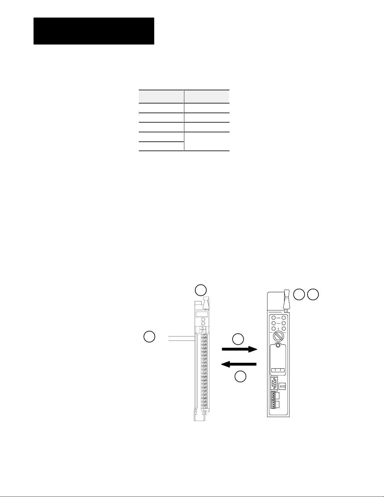
mode of operation (Figure 1.1).
1. The processor transfers your configuration data to the module via a
block transfer write instruction.
2. External devices generate analog signals that are transmitted to the
module.
Figure 1.1
Communication
+
2
Between Processor and Module
3
I/O Chassis
Backplane
4
1
Input Module
Cat. No. 1771IFE
56
PC Processor
10947I
1-2
Page 12

Chapter 1
Overview of the Analog Input Module
3. The module converts analog signals into binary or BCD format, and
stores theses values until the processor requests their transfer.
4. When instructed by your ladder program, the processor performs a
read block transfer of the values and stores them in a data table.
5. The processor and module determine that the transfer was made
without error, and that input values are within specified range.
6. Your ladder program can use and/or move the data (if valid) before it
is written over by the transfer of new data in a subsequent transfer.
7. Your ladder program should allow write block transfers to the module
only when enabled by operator intervention or at power-up.
Accuracy
Chapter Summary
The accuracy of your input module is described in Appendix A.
In this chapter you read about the functional aspects of the input module
and how the module communicates with the programmable controller.
1-3
Page 13

Chapter
Installing the Input Module
2
Chapter
Objectives
Before You Install Your Input
Module
This chapter gives you information on:
calculating the chassis power requirement
choosing the module’s location in the I/O chassis
keying a chassis slot for your module
wiring the input module’s field wiring arm
configuring your module configuration plugs
installing the input module
Before installing your input module in the I/O chassis:
You need to: As described under:
Calculate the power requirements of all modules in
each chassis.
Determine where to place the module in the I/O
chassis.
Key the backplane connector in the I/O chassis. Module Keying, page 22.
Make connections to the wiring arm.
Power Requirements, page 22.
Module Location in the I/O Chassis,
page 22.
Wiring Your Input Module, page 23
and Grounding, page 28.
Electrostatic Damage
Electrostatic discharge can damage semiconductor devices inside this
module if you touch backplane connector pins. Guard against electrostatic
damage by observing the following precautions:
ATTENTION: Electrostatic discharge can degrade
performance or cause permanent damage. Handle the module as
stated below.
Wear an approved wrist strap grounding device, or touch a grounded
object to rid yourself of electrostatic charge before handling the module.
Handle the module from the front, away from the backplane connector.
Do not touch backplane connector pins.
Keep the module in its static-shield bag when not in use.
2-1
Page 14

Chapter 2
Installing the Input Module
Power Requirements
Module Location in the I/O
Chassis
Your module receives its power through the 1771 I/O power supply. The
module requires 750mA from the backplane.
Add this current to the requirements of all other modules in the I/O chassis
to prevent overloading the chassis backplane and/or backplane power
supply.
Place your module in any I/O module slot of the I/O chassis except for the
extreme left slot. This slot is reserved for PC processors or adapter
modules.
Group your modules to minimize adverse affects from radiated electrical
noise and heat. We recommend the following.
Group analog input and low voltage dc modules away from ac modules
or high voltage dc modules to minimize electrical noise interference.
Do not place this module in the same I/O group with a discrete
high-density I/O module when using 2-slot addressing. This module
uses a byte in both the input and output image tables for block transfer.
After determining the module’s location in the I/O chassis, connect the
wiring arm to the pivot bar at the module’s location.
Module Keying
2-2
Use the plastic keying bands, shipped with each I/O chassis, for keying I/O
slots to accept only one type of module.
The module is slotted in two places on the edge of the rear circuit board.
The position of the keying bands on the backplane connector must
correspond to these slots to allow insertion of the module. You can key
any connector in an I/O chassis to receive this module except for the
leftmost connector reserved for adapter or processor modules. Place
keying bands between the following numbers labeled on the backplane
connector (Figure 2.1):
between 10 and 12
between 24 and 26
Page 15
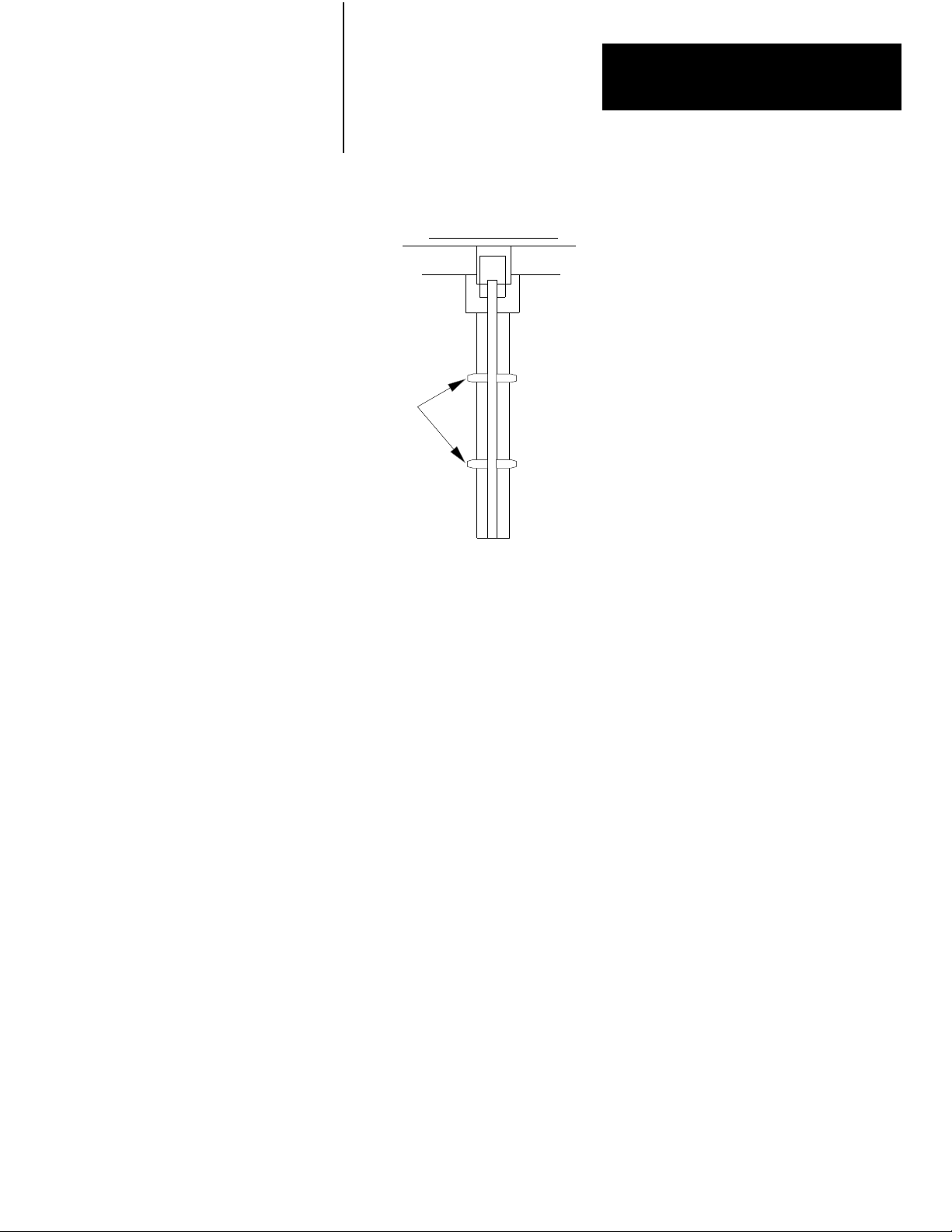
Figure 2.1
Positions
Keying
Keying
Bands
2
4
6
8
10
12
14
16
18
20
22
24
26
28
30
32
34
36
Chapter 2
Installing the Input Module
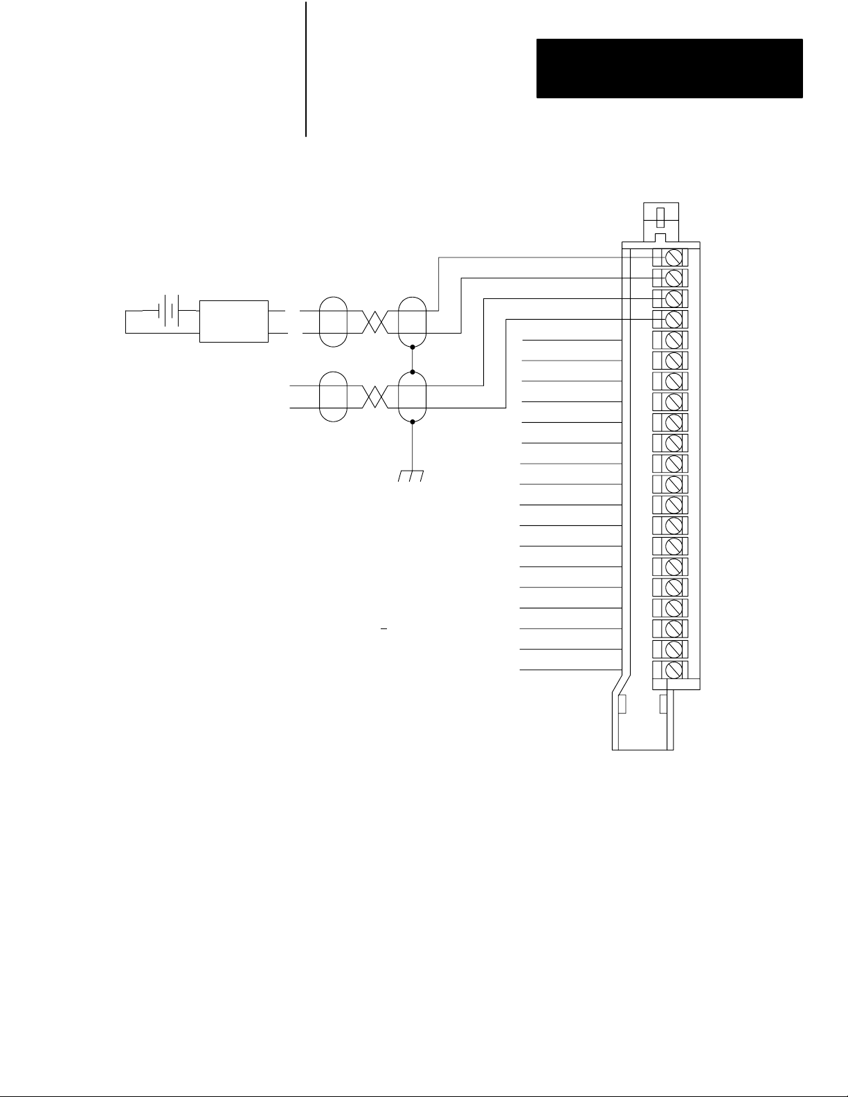
Wiring Your Input Module
1771IFE
12676
Connect your I/O devices to the cat. no. 1771-WG wiring arm shipped
with the module. Attach the wiring arm to the pivot bar at the bottom of
the I/O chassis. It pivots upward and connects with the module so you can
install or remove the module without disconnecting the wires.
Input connections for the 1771-IFE with single-ended inputs are shown in
Figure 2.2 and Figure 2.3. Input connections for the 1771-IFE with
differential inputs are shown in Figure 2.4 and Figure 2.5.
Recommended maximum cable length for voltage-mode input devices is
50 feet. This recommendation is based on considerations of signal
degradation and electrical noise immunity in typical industrial
environments. Cable length for current-mode input devices need not be as
restrictive because analog signals from these devices are less sensitive to
electrical noise interference.
The 1771-IFE module is shipped from the factory set for a 1 to 5V DC
voltage input. Refer to “Changing Your Module’s Configuration”on page
2-9 for other combinations of current and voltage inputs.
2-3
Page 16
Chapter 2
Installing the Input Module
Figure 2.2
Connection
Diagram for 16 Singleended Inputs and T
Transmitters
2Wire
Transmitter
+
–
+
–
Source
1
All commons are electrically tied
together inside the module.
2
Jumper all unused channels to
module common to reduce noise.
Attention: Analog input signals must be within +14.25V
referenced
common
and module common. If an input terminal
channeltochannel crosstalk can cause invalid input
readings and invalid underrange or overrange bits.
The 1771IFE module does not supply loop power for the input
device. The user must supply loop power for looppowered
input devices.
to module common.
This input signal includes any
mode voltage present between either input
exceeds this range,
terminal
Ground
woWire
Channel 1
Channel 2
2
Channel 3
Channel 4
1
Module Common
Channel 5
Channel 6
Channel 7
Channel 8
1
Module Common
Channel 9
Channel 10
Channel 11
Channel 12
1
Module Common
Channel 13
Channel 14
Channel 15
Channel 16
1
Module Common
1
Module Common
1
2
3
4
5
6
7
8
9
10
11
12
13
14
15
16
17
18
19
20
21
1771WG
Field Wiring Arm
10948I
2-4
Page 17
Chapter 2
Installing the Input Module
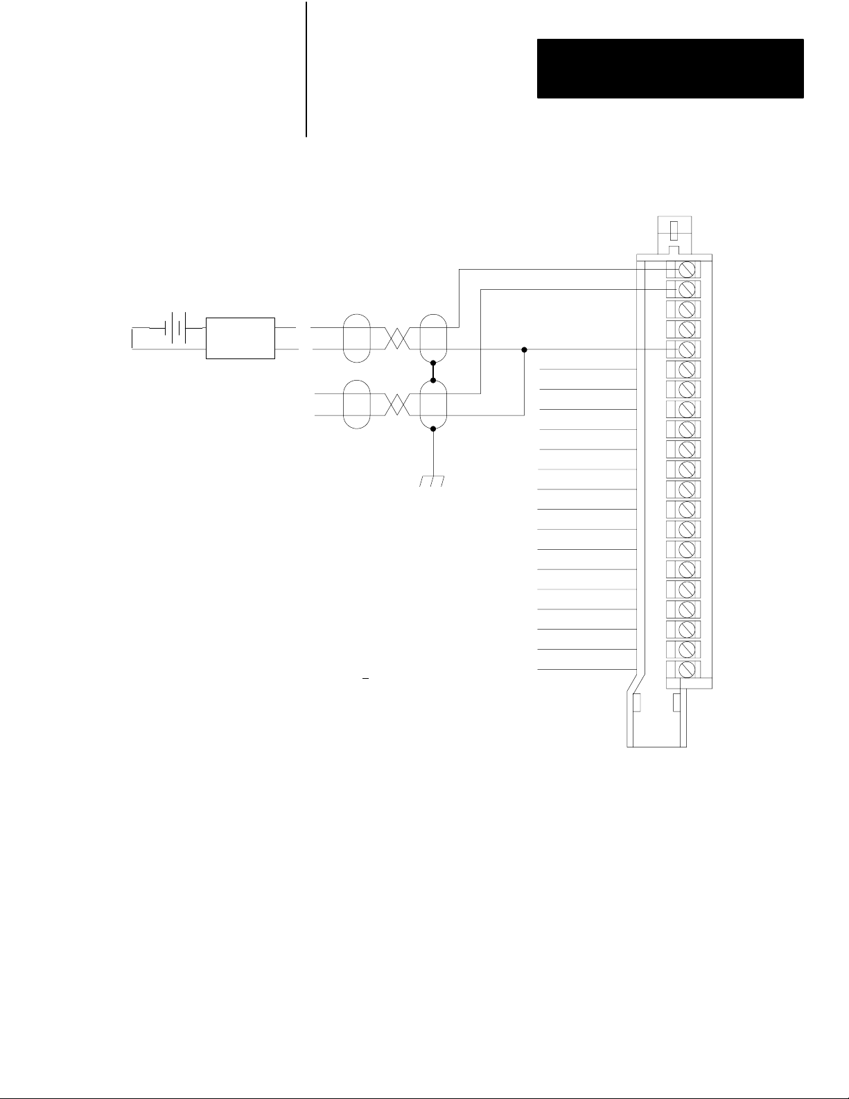
Figure 2.3
Connection
Diagram for 16 Singleended Inputs and FourW
Transmitters
+
–
4Wire
Transmitter
+
–
+
–
Source
1
All commons are electrically tied
together inside the module.
2
Jumper all unused channels to
module common to reduce noise.
Attention: Analog input signals must be within +14.25V
referenced
common
and module common. If an input terminal
channeltochannel crosstalk can cause invalid input
readings and invalid underrange or overrange bits.
The 1771IFE module does not supply loop power for the input
device. The user must supply loop power for looppowered
input devices.
to module common.
This input signal includes any
mode voltage present between either input
exceeds this range,
terminal
Ground
Channel 1
Channel 2
2
Channel 3
Channel 4
1
Module Common
Channel 5
Channel 6
Channel 7
Channel 8
1
Module Common
Channel 9
Channel 10
Channel 11
Channel 12
1
Module Common
Channel 13
Channel 14
Channel 15
Channel 16
1
Module Common
1
Module Common
ire
1
2
3
4
5
6
7
8
9
10
11
12
13
14
15
16
17
18
19
20
21
1771WG
Field Wiring Arm
10948I
2-5
Page 18
Chapter 2
Installing the Input Module
2Wire
Transmitter
Figure 2.4
Connection
+
–
+
–
Diagram for 8 Differential Inputs and T
Source Ground
NOTE:
1. Unused channels must have their + and inputs jumpered
together and tied to module common to reduce noise.
Attention: Analog input signals must be within +14.25V
referenced
to module
range, channeltochannel crosstalk can cause invalid input
readings and invalid underrange or overrange bits.
common. If an input channel exceeds this
woW
Channel 1+
Channel 1
Channel 2+
Channel 2
Not used
Channel 3+
Channel 3
Channel 4+
Channel 4
Not used
Channel 5+
Channel 5
Channel 6+
Channel 6
Not used
Channel 7+
Channel 7
Channel 8+
Channel 8
Module Common
Module Common
ire T
ransmitters
1
2
3
4
5
6
7
8
9
10
11
12
13
14
15
16
17
18
19
20
21
2-6
The 1771IFE module does not supply loop power for the input
device. The user must supply loop power for looppowered
input devices.
Configuring the module for differential inputs does not provide isolation.
1771WG
Field Wiring Arm
10949I
Page 19
Chapter 2
Installing the Input Module
Figure 2.5
Connection
+
–
4Wire
Transmitter
+
–
+
–
Diagram for 8 Differential Inputs and FourW
Source
NOTE:
1. Unused channels must have their + and inputs jumpered
together and tied to module common to reduce noise.
Attention: Analog input signals must be within +14.25V
referenced
range, channeltochannel crosstalk can cause invalid input
readings and invalid underrange or overrange bits.
The 1771IFE module does not supply loop power for the input
device. The user must supply loop power for looppowered
input devices.
to module
common. If an input channel exceeds this
Ground
Channel 1+
Channel 1
Channel 2+
Channel 2
Not used
Channel 3+
Channel 3
Channel 4+
Channel 4
Not used
Channel 5+
Channel 5
Channel 6+
Channel 6
Not used
Channel 7+
Channel 7
Channel 8+
Channel 8
Module Common
Module Common
ire T
ransmitters
1
2
3
4
5
6
7
8
9
10
11
12
13
14
15
16
17
18
19
20
21
Configuring the module for differential inputs does not provide isolation.
1771WG
Field Wiring Arm
10949-I
2-7
Page 20

Chapter 2
Installing the Input Module
Grounding
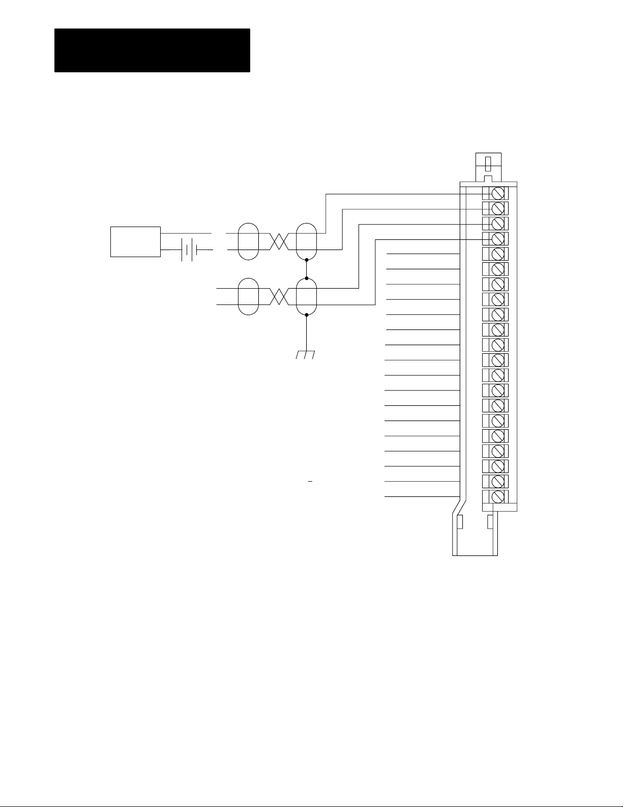
When using shielded cable wire, ground the foil shield and drain wire only
at one end of the cable. We recommend that you wrap the foil shield and
drain wire together and connect them to a chassis mounting bolt
(Figure 2.6). At the opposite end of the cable, tape exposed shield and
drain wire with electrical tape to insulate it from electrical contact.
Figure 2.6
Cable
Remove a length of cable
jacket from the Belden 8761
cable.
Belden
8761 Cable
When you connect grounding conductors to the I/O chassis
grounding stud, place a star washer under the first lug, then
place a nut with captive lock washer on top of each ground lug.
Pull the foil shield and bare
drain wire from the insulated
wires.
Foil
shield
Chassis Ground Singlepoint Grounding
Grounding
Bare
drain
wire
Insulated
wires
Twist the foil shield and drain
wire together to form a single
strand.
Attach a ground lug.
20104
Grounding Stud
I/O Chassis Side Plate
2-8
Star
Washer
1
Use
the cup washer if crimpon lugs are not used.
Ground Lug
Nut
Nut and Captive
Washer
Ground Lug
Shield and Drain
twisted together
1
19480
Shield and Drain
twisted together
#10 Threadforming screw
Externaltooth Washers
Refer
to Wiring and Grounding Guidelines, publication 17704.1 for additional information.
19923
Page 21

Chapter 2
Installing the Input Module
Changing the Module's
Configuration
The analog input module (1771-IFE) has configuration plugs for
determining the input type (voltage or current) desired for each input. The
module comes from the factory with the plugs positioned for
voltage inputs.
To set the configuration plugs for your desired inputs, proceed as follows:
1. Remove the module’s covers by removing the four screws securing
the covers to the module.
2. Locate the selection plugs (Figure 2.7).
Figure 2.7
Configuration
Plug Locations
Selection Plugs
(refer to Figures 2.8, 2.9 and 2.10)
10950I
3. Position the plugs as shown in the Figures for your particular module
(Figures 2.8, 2.9 and 2.10).
4. Reassemble the module after you have finished checking and/or
setting the selection plugs.
2-9
Page 22

Chapter 2
Installing the Input Module
Figure 2.8
Selection
Plug Settings for Differential or Singleended V
Differential or Singleended Current Inputs
Voltage
Differential or Singleended
storage positions
[1] [1] [1]
1
5
9
Differential Current
storage positions storage positions
1
5
9
Current
channel 1
channel 2
13
17
21
13
17
21
channel 3
channel 4
25
25
oltage or
Singleended Current
1
5
9
13
17
21
25
channel 1
channel 2
channel 3
channel 4
channel 5
channel 6
channel 7
channel 8
29
33
37
41
45
49
12677 12678
[1]
Positions 1 and 2 are not used.
Note:
Plugs are not needed for operation in the voltage mode.
29
33
37
41
45
49
channel 5
channel 6
channel 7
channel 8
29
33
37
41
45
49
channel 9
channel 10
channel 11
channel 12
channel 13
channel 14
channel 15
channel 16
10951I
2-10
Page 23

Chapter 2
Installing the Input Module
Figure 2.9
Configuration Plug Settings for Singleended Voltage and Current Inputs
on Adjacent Channels
[1]
1
channel 1 (single-ended voltage)
5
channel 2 (single-ended current)
9
channel 3 (single-ended current)
channel 4 (single-ended voltage)
13
positions 1 and 2 are not used[1]
Figure 2.10
Configuration Plug Settings for Differential Voltage and Current Inputs
on Adjacent Channels
[1]
1
5
channel 1 (differential current)
9
channel 2 (differential voltage)
13
10952I
Note: Either dif
positions 1 and 2 are not used[1]
10953I
ferential and singleended configurations must be selected for the entire module.
2-11
Page 24

Chapter 2
Installing the Input Module
Module Installation
When installing your module in an I/O chassis:
1. First, turn off power to the I/O chassis.
ATTENTION: Remove power from the 1771 I/O chassis
backplane and wiring arm before removing or installing an I/O
module.
Failure to remove power from the backplane could cause injury or
equipment damage due to possible unexpected operation.
Failure to remove power from the backplane or wiring arm could
cause module damage, degradation of performance, or injury.
2. Place the module in the plastic tracks on the top and bottom of the
slot that guides the module into position.
3. Do not force the module into its backplane connector. Apply firm
even pressure on the module to seat it properly.
4. Snap the chassis latch over the top of the module to secure it.
5. Connect the wiring arm to the module.
Indicator Lights
Chapter Summary
The front panel of the input module contains a green RUN and a red FLT
(fault) indicator (Figure 2.11). At power-up an initial module self-check
occurs. If there is no fault, the red indicator turns off. The green indicator
will be on when the module is powered. If a fault is found initially or
occurs later, the red FLT indicator lights. Possible module fault causes and
corrective action is discussed in Chapter 7, Troubleshooting.
Figure 2.11
Diagnostic
ANALOG
(12
RUN
FLT
Indicators
IN
BIT)
Green RUN indicator
Red FLT indicator
10528I
In this chapter you learned how to install your input module in an existing
programmable controller system and how to wire to the field wiring arm.
2-12
Page 25

Module Programming
Chapter
3
Chapter
Objectives
Block Transfer
Programming
In this chapter we describe:
block transfer programming
sample programs in the PLC-2, PLC-3 and PLC-5
processors
module scan time issues
Your module communicates with your processor through bidirectional
block transfers. This is the sequential operation of both read and write
block transfer instructions.
The block transfer write (BTW) instruction is initiated when the analog
module is first powered up, and subsequently only when the programmer
wants to write a new configuration to the module. At all other times the
module is basically in a repetitive block transfer read (BTR) mode.
The application programs for the three processor families were written to
accomplish this handshaking in the described manner. They are minimum
programs; all the rungs and conditioning must be included in your
application program. If you wish to disable BTRs for any reason, or add
interlocks to the BTW rung to prevent writes from happening at certain
times, you are allowed to do it. You may not eliminate any storage bits or
interlocks that are included in our examples. If interlocks are removed, the
program may not work properly.
The analog input module will work with a default configuration of
zeroes entered in all five words of a five word BTW configuration
block. See the configuration default section to understand what this
configuration will look like. Also, refer to Appendix B for example
configuration blocks and instruction addresses to get started.
ATTENTION: In PLC-2 family processors you must not
enable both the read and write instructions at the same time.
Undesirable data could transfer, resulting in unpredictable
machine operation. Using the prescribed programs will prevent
this situation.
3-1
Page 26

Chapter 3
Module Programming
PLC2 Programming
Rung 1
Block transfer read buffer: the
filetofile move instruction holds the
block transfer read (BTR) data (file A)
until the processor checks the data
integrity. If the data was successfully
transferred, the processor energizes
the BTR done bit, initiating a data
transfer to the buffer (file R) for use in
the program.
If the data is corrupted during the BTR
operation, the BTR done bit is not
energized and data is not transferred to
the buffer file. In this case, the data in
the BTR file will be overwritten by data
from the next BTR.
Rungs 2 and 3
These rungs provide for a userinitiated
block transfer write (BTW) after the
module is initialized at powerup.
Pressing the pushbutton locks out BTR
operation and initiates a BTW that
reconfigures the module. Block transfer
writes will continue for as long as the
pushbutton remains closed.
Rungs 4 and 5
These rungs provide a readwriteread"
sequence to the module at powerup.
They also make sure that only one
block transfer (read or write) is enabled
during a particular program scan.
Rungs 6 and 7
These rungs are the conditioning block
transfer rungs. Include all the input
conditioning shown in the example
program.
The PLC-2 program example regulates when each block transfer will be
initiated to eliminate problems caused by limited regulation of
bidirectional block transfers. Both storage bits are needed, as shown in the
example, to accomplish this task in all PLC-2 systems, local or remote,
with long or short program scans. Therefore, the program as shown is the
minimum required. Note that PLC-2 processors that do not have the block
transfer instruction must use the GET-GET block transfer format which is
outlined in Appendix E.
Figure 3.1
PLC2
Block Transfer Read
Done Bit
1
Pushbutton [1]
2
Block Transfer Write
Done Bit Pushbutton [1]
3
Block Transfer Write
Done Bit
4
Block Transfer Read
Done Bit
5
Power-up
6
7
Bit
Storage
Bit B
Power-up
Bit
Storage
Bit A
Family Sample Program Structure
FILE TO FILE MOVE
COUNTER ADDR:
POSITION:
FILE LENGTH:
FILE A:
FILE R:
RATE PER SCAN
Power-up
Bit
Storage
Bit A
[1] You can replace the pushbutton with a timer done" bit to initiate the block transfer
write on a timed basis. You can also use any storage bit in memory.
BTR Done
Bit
Storage
Bit B
BTR
BLOCK XFER READ
DATA ADDR:
MODULE ADDR:
BLOCK LENGTH:
FILE:
BTW
BLOCK XFER WRITE
DATA ADDR:
MODULE ADDR:
BLOCK LENGTH:
FILE:
YYYY - XXXX
YYYY - XXX
XXXX - XXXX
XXX
XXX
XXX
XXX - XXX
XXX
XXX
RGS
XX
XXX
RGS
XX
ENABLE
DONE
ENABLE
EN
17
DONE
DN
15
Storage
Bit A
L
Storage
Bit A
U
Storage
Bit B
L
Storage
Bit B
U
ENABLE
EN
X7
DONE
DN
X7
EN
X6
DN
X6
10954I
3-2
Page 27

Chapter 3
Module Programming
PLC3 Programming
Program Action
At powerup, the user program examines, the
BTR done bit in the block transfer read file,
initiates a block transfer write to configure the
module, and then does consecutive block
transfer reads continuously. The powerup bit
can be examined and used anywhere in the
program.
Rungs 1 and 2
Rungs 1 and 2 are the block transfer read and
write instructions. The BTR done bit in rung 1,
being false, initiates the first read block transfer.
After the first read block transfer, the module
performs a block transfer write and then does
continuous block transfer reads until the
pushbutton is used to request another block
transfer write. After this single block transfer
write is performed, the module returns to
continuous block transfer reads automatically.
Block transfer instructions with the PLC-3 processor use one binary file in
a data table section for module location and other related data. This is the
block transfer control file. The block transfer data file stores data that you
want transferred to your module (when programming a block transfer
write) or from your module (when programming a block transfer read).
The address of the block transfer data files are stored in the block transfer
control file.
The industrial terminal prompts you to create a control file when a block
transfer instruction is being programmed. The same block transfer
control file is used for both the read and write instructions for your
module. A different block transfer control file is required for every
module.
A sample program segment with block transfer instructions is shown in
Figure 3.2, and described below.
Figure 3.2
Family Sample Program Structure
PLC3
Block Transfer
1
2
Read
Done Bit
Pushbutton
Power-up
Bit
Block Transfer
Write
Done Bit
BTR
BLOCK XFER READ
RACK:
GROUP:
MODULE:
DATA:
LENGTH =
CNTL:
XXXXX=XXXX
XXXXX:XXXX
BTW
BLOCK XFER WRITE
RACK :
GROUP :
MODULE:
DATA:
LENGTH =
CNTL:
XXXXX = XXXX
XXXXX:XXXX
X=XXXX
X = XXXX
XXX
XXX
X
X
X
X
ENABLE
EN
12
DONE
DN
15
ERROR
ER
13
ENABLE
EN
02
DONE
DN
05
ERROR
ER
03
3-3
Page 28

Chapter 3
Module Programming
PLC5 Programming
Program Action
Rungs 1 and 2
At powerup, the program enables a block
transfer read and examines the powerup bit
in the BTR file (rung 1). Then, it initiates one
block transfer write to configure the module
(rung 2). Thereafter, the program continuously
reads data from the module (rung 1).
A subsequent BTW operation is enabled by a
pushbutton switch (rung 2). Changing
processor mode will not initiate a block
transfer write.
The PLC-5 program is very similar to the PLC-3 program with the
following exceptions:
1. You must use enable bits instead of done bits as the conditions on
each rung.
2. A separate control file must be selected for each of the block transfer
instructions. Refer to Appendix B.
Figure 3.3
Family Sample Program Structure
PLC5
BTR Enable
1
2
Bit
Pushbutton
Power-up Bit
BTW Enable
BTR
BLOCK TRANSFER READ
RACK:
GROUP:
MODULE:
CONTROL:
DATA FILE:
LENGTH:
CONTINUOUS:
BTW
BLOCK TRANSFER WRITE
RACK:
GROUP:
MODULE:
CONTROL:
DATA FILE:
LENGTH:
CONTINUOUS:
XX:XX
XX:XX
XX:XX
XX:XX
EN
X
X
DN
X
ER
X
N
EN
X
X
DN
X
ER
X
N
3-4
10956I
Page 29

Chapter 3
Module Programming
Module
Scan T
ime
Scan time is defined as the amount of time it takes for the input module to
read the input channels and place new data into the data buffer. Scan time
for your module is shown in Appendix A.
The following description references the sequence numbers in Figure 3.4.
Following a block transfer write “1” the module inhibits communication
until after it has configured the data “2,” performed self-calibration “3,”
scanned the inputs “4,” and filled the data buffer “5.” Write block transfers,
therefore, should only be performed when the module is being configured
or calibrated.
Any time after the second scan begins “6,” a BTR request “7” can be
acknowledged. This interrupts the scan and the BTR empties the buffer.
Following the BTR, the input module inhibits block transfer
communications with the programmable controller until it has scanned its
inputs “8” and new data is ready ”9.” The input module repeats the scan
sequence “10,” updating the input values until another block transfer
request is received. Therefore, BTRs will only be completed as frequently
as the total scan time of the input module.
Figure 3.4
T
Block
ransfer T
ime
Chapter Summary
End of block
transfer write
Block
Transfer
Write
time
1 2 3 4 56789
Note: Configure/Calibration time:
Configure
time
Singleended mode = 100ms without filter, 102ms with filter
Differential mode = 56ms without filter, 58ms with filter
Scan time:
= 12.5 ms for 8 differential inputs (no scaling or digital filter);
= 25 ms for 16 singleended inputs (no scaling or digital filter)
Calibration
time
See note
Module available to
perform block transfer
1st
Scan
2nd
Scan
3rd
Scan
In this chapter, you learned how to program your programmable controller.
You were given sample programs for your PLC-2, PLC-3 and PLC-5
family processors.
You also read about module scan time.
10
12689
3-5
Page 30

Configuring Your Module
Chapter
4
Chapter
Objectives
Configuring Your Input
Module
In this chapter you will read how to configure your module’s features,
condition your inputs and enter your data.
Because of the many analog devices available and the wide variety of
possible configurations, you must configure your module to conform to the
analog device and specific application that you have chosen. Data is
conditioned through a group of data table words that are transferred to the
module using a block transfer write instruction. Before continuing, make
sure you read “Setting Module Selection Plugs” in chapter 2.
The software configurable features available with the Analog Input
Module (cat. no. 1771-IFE) are:
input range selection
input type
data format
digital filtering
real time sampling
scaling to engineering units
Note that digital filtering and scaling values must be entered in BCD
format only. Change your display format to BCD in the PLC-5 and
PLC-3 to accomplish this.
Note: Programmable controllers that use 6200 software programming tools
can take advantage of the IOCONFIG utility to configure this module.
IOCONFIG uses menu-based screens for configuration without having to
set individual bits in particular locations. Refer to your 6200 software
literature for details.
Note: Programmable controllers that use process configuration and
operation software (cat. no. 6190–PCO) can take advantage of those
development and runtime tools used for the application of programmable
controllers in process control. The PCO worksheets and the menu-driven
configuration screens and faceplates let you configure, test/debug and
operate the I/O module. Refer to your 6190-PCO software literature for
details.
4-1
Page 31

Chapter 4
Module Configuration
Input Range Selection
You can configure the module to operate with any of five voltage or three
current ranges. You can select individual channel ranges using the
designated words of the write block transfer instruction (Table 4.A). Use
BTW word 1 for range selection of channels 1 through 8, and BTW word 2
for channels 9 through 16. Two bits are allocated for each channel. For
example, for channel 1, set word 1 bits 00-01 as shown in Table 4.A.
Table 4.A
Range Selection Bits
Input
Bit 01 Bit 00 Voltage or current input
0 0 1 to 5 V DC, 4 to 20 mA
0 1 0 to 5 V DC, 0 to 20 mA
1 0 5 to +5 V DC, 20 to +20 mA
1 1 10 to +10 V DC2, 0 to 10 V DC
1
Current input mode selected by configuration plug.
2
Configurable
using bipolar scaling.
1
1
1,2
Table 4.B shows the incremented voltage or current assigned to each bit for
the seven different input ranges. For example, if the channel 1 input range
is 0 to +5V and the actual incoming signal is at mid-range (+2.5V) the
value in the module’s data word would be 0000 1000 0000 0000 (binary)
or 2048 (decimal). The input is 2048/4096, or 1/2 of full scale.
Table 4.B
V
oltage and Current Ranges for the Analog Input Module
Input
Nominal Voltage or
Current Range
+1 to +5V 0000 to +4095 0000 to + 4095 0.98mV
0 to 5V 0000 to +4095 0000 to +4095 1.22 mV
5 to +5V 4095 to +4095 4095 to +4095 1.22mV
10 to +10V 4095 to +4095 4095 to +4095 2.44mV
0 to +20mA 0000 to +4095 0000 to +4095 .0049mA
+4 to +20mA 0000 to +4095 0000 to +4095 .0039mA
20 to +20mA 4095 to +4095 4095 to +4095 .0049 mA
Note: Voltage
and current input ranges are selectable on a per channel basis.
Corresponding 4Digit
BCD Output Range
Corresponding 12Bit
Binary Output Range
Current Per Bit
Voltage or
4-2
Page 32

Chapter 4
Module Configuration
Input Type
Data Format
You can select single-ended or differential inputs using the designated bit
in the configuration file. Inputs to a particular module must be all
single-ended or all differential. Set BTW word 3, bit 08 (bit 10 octal) as
shown in Table 4.C.
Table 4.C
Selecting
Decimal Bit 8
(Octal Bit 10)
Singleended or Differential Inputs
Input type
1 differential inputs
0 singleended inputs
You must also indicate what format will be used to read data from your
module. Typically, you select BCD with PLC-2 processors, and 2’s
complement binary with PLC-3 and PLC-5 processors. See Appendix C
for details on data format. You use BTW word 3 bits 09-10 (11-12 octal) to
set the data format (Table 4.D).
Table 4.D
Selecting
the Data Format
Decimal Bit 10
(Octal Bit 12)
0 0 BCD
0 1 not used
1 0 two's complement binary
1 1 signed magnitude binary
Decimal Bit 09
(Octal Bit 11)
Data Format
4-3
Page 33

Chapter 4
Module Configuration
Digital Filtering
The module has hardware-based high frequency filters on all channels to
reduce the effect of electrical noise on the input signal. Software digital
filtering is meant to reduce the effect of process noise on the input signal.
Digital filtering is selected using BTW word 3, bits 00-07.
The digital filter equation is a classic first order lag equation (Figure 4.1).
Using a step input change to illustrate the filter response (Figure 4.2), you
can see that when the digital filter constant time elapses, 63.2% of the total
response is reached. Each additional time constant achieves 63.2% of the
remaining response.
Figure 4.1
Filter Equation
Digital
t
(X
Yn = Y
Where:
- Y
+
n-1
t + TA
Y
n = present output, filtered peak voltage (PV)
Y
n -1 = previous output, filtered PV
t = module channel update time (seconds)
TA
= digital filter time constant (seconds)
X
n = present input, unfiltered PV
n
n-1
)
Figure 4.2
Digital Filter Lag Equation Illustration
100%
63%
Amplitude
0
0 0.01 0.5 0.99 Time in Seconds
Unfiltered Input
TA = 0.01 sec
TA = 0.5 sec
TA = 0.99 sec
16723
Digital filter time constant values of 0.00 BCD to 0.99 BCD (0.00 BCD =
no filter; 0.99 BCD = maximum filter) are set in bits 00 through 07 of
word 3 of the block transfer write instruction. If an invalid digital filter
value is entered (i.e., 0.1F), bit 02, word 1 of the block transfer read
instruction will be set. If an invalid digital filter value is entered, the
module will not perform digital filtering. If you use the digital filtering
feature, the filter time constant value chosen will apply to all input signals.
4-4
Page 34

Chapter 4
S
d
S
d
Module Configuration
Real Time Sampling
The real time sampling (RTS) mode of operation provides data gathered at
precisely timed intervals for use by the processor. BTW word 3 bits 11–15
(13–17 octal) are used to set the real time sampling interval.
RTS is invaluable for time based functions (such as PID and totalization) in
the PLC. It allows accurate time based calculations in local or remote I/O
racks. In the RTS mode the module scans and updates its inputs at a user
defined time interval (T) instead of the default interval. The module
ignores block transfer read (BTR) requests for data until the sample time
period elapses. The BTR of a particular data set occurs only once at the
end of the sample period and subsequent requests for transferred data are
ignored by the module until a new data set is available. If a BTR does not
occur before the the end of the next RTS period, a time-out bit is set in the
BTR status area. When set, this bit indicates that at least one data set was
not transferred to the processor. (The actual number of data sets missed is
unknown.) The time-out bit is reset at the completion of the BTR.
Set appropriate bits in the BTW data file to enable the RTS mode. You can
select RTS periods ranging from 100 milliseconds (ms) to 3.1 seconds.
Refer to Table 4.E below for actual bit settings. Note that the default mode
of operation is implemented by placing all zeroes in bits 11–15
(13–17 octal).
Decimal Bits 15 14 13 12 11
Octal Bits 17 16 15 14 13
0 0 0 0 0 No RTS, Default settings 1 0 0 0 0 1.6s
0 0 0 0 1 100ms 1 0 0 0 1 1.7s
0 0 0 1 0 200ms 1 0 0 1 0 1.8s
0 0 0 1 1 300ms 1 0 0 1 1 1.9s
0 0 1 0 0 400ms 1 0 1 0 0 2.0s
0 0 1 0 1 500ms 1 0 1 0 1 2.1s
0 0 1 1 0 600ms 1 0 1 1 0 2.2s
0 0 1 1 1 700ms 1 0 1 1 1 2.3s
0 1 0 0 0 800ms 1 1 0 0 0 2.4s
0 1 0 0 1 900ms 1 1 0 0 1 2.5s
0 1 0 1 0 1.0s 1 1 0 1 0 2.6s
0 1 0 1 1 1.1s 1 1 0 1 1 2.7s
0 1 1 0 0 1.2s 1 1 1 0 0 2.8s
0 1 1 0 1 1.3s 1 1 1 0 1 2.9s
0 1 1 1 0 1.4s 1 1 1 1 0 3.0s
0 1 1 1 1 1.5s 1 1 1 1 1 3.1s
Default
Settings =
Singleended inputs 25 ms
Dif
ferential inputs 12.5 ms
Table 4.E
Settings for the Real T
Bit
ample Time Perio
ime Sample Mode
15 14 13 12 11
ample Time Perio
17 16 15 14 13
4-5
Page 35

Chapter 4
Module Configuration
Scaling
Your module can perform linear conversion of unscaled data to
engineering units, (for example; gallons/minute, degrees C/degrees F and
pounds/square inch). Unscaled data in the module has a range of : 0
through 4095 for the polar ranges (0 to 5V DC/0 to 20mA and 1 to 5V
DC/4 to 20mA); and -4095 to +4095 (8190) for the bipolar ranges
(+
5V/+20mA and +10V). BTW words 6 through 37 are the scaling words
for channels 1 through 16. Channel 1 minimum scaling values are set in
word 6, and maximum scaling values are set in word 7. Channel 2
minimum scaling values are set in word 8, and maximum scaling values
are set in word 9, and so on for the other channels.
The format of this data is 4-digit BCD or 12-bit binary. The resolution at
the module of scaled values is the same as for unscaled data: one part in
4095 for 0 to 5V DC/0 to 20mA and 1 to 5V DC/4 to 20mA ranges; and
one part in 8190 for the +
processor, however, is determined by the scaled ranges (i.e., if 0 =
minimum and 500 = maximum, resolution is now 1 part in 500). Each
input channel can be scaled independently of the other channels.
Note: To achieve the 0 to +10V range you must use bipolar scaling. Select
the +
10V range and scale for + the actual intended range. If you need 0 to
100 gpm, set scaling values at -100 and +100. You will effectively be
creating a 0 to 10V range that is scaled from 0 to 100.
5V/+20mA and +10V ranges. Resolution at the
Implementing the Scaling Feature
You implement the scaling feature by:
1. Inserting minimum and maximum scaled values in the appropriate
configuration words
2. If any of the minimum or maximum values are negative, set the
appropriate sign bits in the minimum or maximum sign bit word
3. If a single channel is scaled, all channels must be scaled, and all 37
configuration words must be written to the module.
Scaling Ranges
The maximum range of the scaling values is +9999 BCD. These values
must be entered in BCD.
Typically, invalid values are “minimum greater than maximum,” or
“minimum equal to maximum.” If invalid values are entered into the
scaling words, the corresponding input in the BTR data will be zero
and the invalid scaling bit will be set.
4-6
Page 36

Chapter 4
Module Configuration
Important: Scaling values must always be entered in BCD format,
even if the data format chosen is binary. If scaling is selected for any
channel, all channels must be scaled. If scaling is not required on certain
channels, set those to the default input range: 0 to 4095 for 0 to + voltage
or current ranges, and -4095 to +4095 for - to + voltage or current ranges.
If scaling is not selected, the module requires specific minimum BTR
file lengths for the number of channels used. The BTW file length can
be set to 3 words. Table 4.F shows the required BTW and BTR file lengths.
Table 4.F
Block
T
ransfer Read and W
rite File Lengths
Channels
Used
1 5 7
2 6 9
3 7 11
4 8 13
5 9 15
6 10 17
7 11 19
8 12 21
9 13 23
10 14 25
11 15 27
12 16 29
13 17 31
14 18 33
15 19 35
16 20 37
BTR File
Length
BTW File
Length
Important: Use decimally addressed bit locations for PLC-5 processors.
4-7
Page 37

Chapter 4
Module Configuration
Default Configuration
If a write block of five words, with all zeroes, is sent to the Analog Input
Module (cat. no. 1771-IFE), default selections will be:
1 to 5V DC or 4 to 20mA (dependent on configuration jumper setting)
BCD data format
no real time sampling (RTS)
no filtering
no scaling
single-ended inputs
Figure 4.3
Input Module (1771IFE) Block T
Analog
Block
Decimal Bits 15 14 13 12 11 10 09 08 07 06 05 04 03 02 01 00
Octal Bits 17 16 15 14 13 12 11 10 07 06 05 04 03 02 01 00
Word 1 8 7 6 5 4 3 2 1 Range Selection Channels 1 thru 8
2 16 15 14 13 12 11 10 9 Range Selection Channels 9 thru 16
3 Real Time Sampling
Data
Format
Input
Type
Digital Filter
ransfer W
rite Configuration
Description
Real time sampling, data format, input
type and digital filter
4 16 15 14 13 12 11 10 9 8 7 6 5 4 3 2 1 Sign Bits, minimum scaling values
5 16 15 14 13 12 11 10 9 8 7 6 5 4 3 2 1 Sign Bits, maximum scaling values
6 Channel 1 minimum scaling
7 Channel 1 maximum scaling
8 Channel 2 minimum scaling
9 Channel 2 maximum scaling
10 Channel 3 minimum scaling
⇓⇓⇓⇓
37 Channel 16 maximum scaling
4-8
Page 38

Word
Chapter 4
Module Configuration
Bit/Word Descriptions for the Analog Input Module Block Transfer
Write Configuration Block
Note that decimal bits are shown, with octal bits in parentheses.
Decimal
Bit
(Octal Bit)
Description
Word 1 and 2
Word 3
Word 4
Word 5
Words 637
Bits 0015
(0017)
Bits 0007
(0007)
Bit 08
(10)
Bits 0910
(0710)
Bits 1115
(1317)
Bits 0015
(0017)
Bits 0015
(0017)
Bits 0015
(0017)
Input range selections allow the user to configure the inputs for any of 7 input
voltage or current ranges. Two bits are required for each channel. See Table 4.A.
Digital filter reduces effect of noise on input. See "Digital Filtering" on page 44.
Input type, set bit for differential mode on all channels.
Reset (0) = singleended. Refer to Table 4.C
Data format matches format of processor. See Table 4.D.
Real time sampling will default to 12.5ms for differential mode and 25ms for
singleended, greater with filtering selected. See appendix A for timing details.
See Table 4.E for other real time intervals.
Minimum sign bits, when set, designate negative minimum scaling values for the
corresponding input channels. Bit 00 corresponds to channel 1, bit 01
corresponds to channel 2, etc.
Maximum sign bits, when set, designate maximum scaling values that are
negative. Maximum scaling value must be greater than minimum on any
particular channel. Bit 00 corresponds to channel 1, bit 01 corresponds to
channel 2, etc.
Minimum and maximum scaling values for each channel. Enter in BCD format.
Chapter Summary
In this chapter you learned how to configure your module’s features,
condition your inputs and enter your data.
4-9
Page 39

Chapter
Module Status and Input Data
5
Chapter
Objectives
In this chapter you will read about:
reading data from your module
block transfer read block format
Reading Data From Your
Module
Block transfer read programming moves status and data from the input
module to the processor’s data table in one I/O scan (Figure 5.1). The
processor’s user program initiates the request to transfer data from the
input module to the processor.
Figure 5.1
Assignments for Analog Input Module (1771IFE)
Word
Block T
ransfer Read
Decimal Bits 15 14 13 12 11 10 09 08 07 06 05 04 03 02 01 00
Description
Octal Bits 17 16 15 14 13 12 11 10 07 06 05 04 03 02 01 00
Word 1 Not Used Diagnostic Bits Diagnostics
2 16 15 14 13 12 11 10 9 8 7 6 5 4 3 2 1 Data underrange for channels 1-16
3 16 15 14 13 12 11 10 9 8 7 6 5 4 3 2 1 Data overrange for channels 1-16
4 16 15 14 13 12 11 10 9 8 7 6 5 4 3 2 1 Data polarity for channels 1-16
Description
1
1
5 Channel 1 Input Channel 1 Input
6 Channel 2 Input Channel 2 Input
7 Channel 3 Input Channel 3 Input
8 Channel 4 Input Channel 4 Input
⇓⇓⇓⇓
20 Channel 16 Input Channel 16 Input
1
These
bits are set (1) at approximately the input range limits selected (
Table 5.B).
5-1
Page 40

Chapter 5
Module Status and Input Data
Block Transfer Read Format
Word 1
Word 2
Word 3
The bit/word description for the block transfer read of the Analog Input
Module is described below in Table 5.A.
Table 5.A
W
ord Format for the Analog Input Module
BTR
Decimal
Word
Bit
(Octal Bit)
Bit 00
Bit 01
Bit 02
Bit 03
Bits 00-15
(00-17)
Bits 00-15
(00-17)
Description
Power up bit is used by the module to tell the processor that it is alive
but not yet configured. It is a key element in the application program.
Out of range bit is sent to tell the processor that one or more
channels are either over or under range.
1
Invalid scaling bit reports that the scaling is somehow invalid.
Usually, both values are equal or minimum is greater than maximum
when this bit comes on. Can also be an invalid filter value.
Real time sample fault bit. This bit is set if the module is configured for
RTS and a block transfer read has not occurred within the
user-programmed period.
Individual underrange bits for each channel. Bit 00 for channel 1, bit
01 for channel 2, etc.
1
These bits are set (1) at approximately the input
range limits selected from Table 5.B.
Individual overrange bits for each channel. Bit 00 for channel 1, bit
01 for channel 2, etc.
1
These bits are set (1) at approximately the
input range limits selected from Table 5.B.
Chapter Summary
Word 4
Bits 00-15
(00-17)
Polarity bits are set when input is less than zero. Bit 00 for channel
1, bit 01 for channel 2, etc.
Word 5 thru 20 Input values. Word 5 for channel 1, word 6 for channel 2, etc.
1
Attention: If
invalid input readings and invalid underrange/overrange bits.
an input terminal'
s voltage exceeds +
14.25V as referenced to module common, channeltochannel crosstalk can cause
Table 5.B
Range Selection
Input
Voltage input Current input
1
1 to 5V dc 4 to 20mA
0 to 5V dc 0 to 20mA
-5 to +5V dc -20 to +20mA
-10 to +10V dc
2
1
2
0 to 10V dc
1
Current input mode selected by configuration plug.
2
Configurable
using bi-polar scaling.
In this chapter you learned the meaning of the status information that the
input module sends to the processor.
5-2
Page 41

Calibrating Your Module
Chapter
6
Chapter
Objectives
Tools and Equipment
Calibration Procedure
In this chapter we tell you what tools you need and how to calibrate your
module.
In order to calibrate your input module you will need the following tools
and equipment:
Equipment Description
Digital voltmeter
Alignment tool
Potentiometer sealant
Industrial terminal
Backplane extender card Cat. no. 1771EZ
The analog input module is shipped from the factory already calibrated.
If necessary to recalibrate the module, you must calibrate the module in an
I/O chassis. The module must communicate with the processor and
industrial terminal. Calibration consists of adjusting the 10V reference and
nulling the input offset.
51/2 digit, 0.01% accuracy minimum: Keithley191 or Fluke
8300A or equivalent
P/n 35F616, for pot adjustment: Newark Electronics,
500 N.Pulaski Rd., Chicago, IL
Torque Seal: Organic Products,
P.O. Box 928, Irving, TX
Cat. no. 1770T3 and program panel interconnect cable
(cat. no. 1772TC) for PLC2 family processors:
AllenBradley,Highland Hts., OH
Important: The module must be powered up for at least 30 minutes before
attempting to calibrate.
ATTENTION: Do not attempt to calibrate your module until
you have read and thoroughly understand this procedure. Also,
do not attempt to calibrate this module in an operating system.
Damage to the equipment or personal injury may result.
6-1
Page 42

Chapter 6
Calibrating Your Module
Adjusting the 10V Reference
1. Turn off power to your processor and I/O chassis.
2. Swing the field wiring arm out of the way.
3. Remove the module from the I/O chassis.
4. Plug the module into the extender card, and insert the extender card
into the I/O chassis.
5. Attach the negative lead to an analog common (pin 5, 10, 15, 20 or
21) of the wiring arm.
6. Attach the positive lead of your voltmeter to TP1.
7. To set the on-board +10V reference, adjust potentiometer R64
(Figure 6.1) until the value at TP1 = 10.0000V (+
.0002V maximum).
Figure 6.1
Test
E1 Jumper in calibration position
1
E1
3
Points and Potentiometers for Analog Input Module (1771IFE)
13
E1
Left
Side of Module
6-2
TP1TP2R64R63
10956I
Page 43

Chapter 6
Calibrating Your Module
Nulling the Input Offset
After completing the 10V reference adjustment, turn off power to your
processor and I/O chassis and complete the following steps.
1. Move jumper E1 (Figure 6.1) from the default position (connecting
the center and right posts) to the calibration position (connecting the
center and left posts).
2. Attach the negative lead of your voltmeter to an analog common (pin
5, 10, 15, 20 or 21) of the field wiring arm.
3. Attach the positive lead of your voltmeter to TP2.
4. Turn on power to your processor and I/O chassis. Check to make
sure the red FLT indicator is lit and the green RUN indicator is off. If
the red indicator is off, check the position of E1.
Chapter Summary
5. Adjust potentiometer R63 (Figure 6.1) until the value at
TP2 = 0.0000V (+
0.0002V maximum).
6. After completing the adjustment, remove power from the I/O chassis
and return jumper E1 to the default position.
In this chapter you learned how to calibrate your module. This included the
necessary tools, adjusting the 10V reference, and nulling the offset.
6-3
Page 44

Chapter
7
Troubleshooting Your Input Module
Chapter
Objective
Diagnostics Reported by the
Module
In this chapter, we describe how to troubleshoot your module by observing
the indicators and by monitoring status bits reported to the processor.
At power-up, the module momentarily turns on the red indicator as a lamp
test, then checks for:
correct RAM operation
firmware errors
Thereafter, the module lights the green RUN indicator when operating
without fault, or lights the red FAULT indicator when it detects fault
conditions. The module also reports status and specific faults (if they
occur) in every transfer of data (BTR) to the PC processor. Monitor the
green and red indicators and status bits in word 1 of the BTR file when
troubleshooting your module.
Figure 7.1
Diagnostic
Indicators
ANALOG
IN
BIT)
(12
RUN
FLT
10528I
Diagnostic Bits Reported By the Analog Input Module
Diagnostic bits in the read block transfer status words provide diagnostic
capabilities.
Word 1 provides power-up and valid data status. Words 2, 3 and 4
provide channel data status.
If a module on-board self test fault occurs, block transfers will be
inhibited, the red fault (FLT) will light, and the green run (RUN) light will
go out.
7-1
Page 45

Chapter 7
Troubleshooting Your Input Module
Word 1
Diagnostics word 1 is the first data word in the read block transfer file for
transfer to the central processor. It contains a power-up bit (bit 00) that is
set (1) when the module is first powered up. It is reset (0) after a write
block transfer. It also contains an under-range or over-range bit (bit 01)
that is set when any input is under or over-range.
An invalid scaling data bit (bit 02) will be set if invalid scaling data is
entered into any of the minimum/maximum scaling value words. Note that
minimum equal to maximum is an invalid value. If invalid values are
entered into the minimum or maximum scaling words the corresponding
read block transfer input channel word will be set to 0000.
Bit 02 will also be set if an invalid digital filter value is entered (e.g., 1F).
If an invalid digital filter value is entered, the module will not perform
digital filtering.
The real time sample (RTS) fault bit (bit 03) is set if the module is
configured for RTS and a block transfer read has not occurred within the
user-programmed period.
Word 2
Word 2 provides for under-range conditions. When a particular channel
input is under-range, the associated bit will be set. As long as inputs are
under range the associated bit will remain set. Bit 00 corresponds to
channel 1, bit 01 to channel 2, etc.
Word 3
Word 3 provides for over-range conditions. When a particular channel
input is over-range, the associated bit will be set. As long as inputs are in
range the associated bit will remain reset. Bit 00 corresponds to channel 1,
bit 01 to channel 2, etc.
Word 4
Word 4 provides an indication of a particular channel’s input polarity (set,
or 1 = negative; reset, or 0 = positive). Bit 00 corresponds to channel 1, bit
01 to channel 2, etc.
Table 7.A lists the probable cause and recommended actions for a number
of common trouble indications.
7-2
Page 46

Chapter 7
Troubleshooting Your Input Module
Legend
Off
On
Table 7.A
Troubleshooting
Indicators Probable Cause Recommended Action
RUN (green)
FLT (red)
RUN (green)
FLT (red)
Chart for Analog Input Module (1771IFE)
Normal operation None
If outofrange bit is set (BTR word 1, bit
02) and all 8 underrange bits are set
(BTR word 2, bits 00 through 07).
If incorrect data in final storage word
locations in processor's data table,
possible severed or disconnected input
cable associated with the affected
channels.
or
Input module is conditioned for BCD
instead of binary or the reverse, incorrect
scaling, sign bits missing, wrong range.
Hardware failure in module Return module for repair.
Return module for repair
Repair/replace cable.
Condition module for desired format
(BCD or binary), enter correct data and
initiate another write block transfer.
If module connections are intact and
configuration data is correct check
calibration procedure.
Chapter Summary
RUN Neither LED
FLT comes on
In this chapter you learned how to interpret the indicator lights, and
troubleshoot your input module.
No power
PICO fuse is bad.
Turn off power. Remove and reinsert
module into chassis. Return power.
If problem still exists, and chassis power
supply is functioning properly, return the
module for repair.
7-3
Page 47

Appendix
A
Specifications
Inputs per module 16 single-ended; 8 differential low level
Module Location 1771 I/O rack - 1 slot
+1 to +5V dc
0 to 5V dc
Input voltage ranges (nominal)
Input current ranges (nominal)
Resolution 12-bit binary
Accuracy 0.1% of full scale range @ 25oC
Linearity +1 LSB
Repeatability +1 LSB
Isolation Voltage +1500V, (transient)
Input overvoltage protection
Input overcurrent protection (current ranges) 30mA
Common mode voltage +14.25 Volts
Input impedance 100 Megohms for voltage ranges; 250 ohms for current ranges
Common mode rejection 80 db, DC-120 Hz
Current Requirements 0.75A @ +5V from I/O chassis backplane
Power Dissipation 3.75 Watts (maximum)
Thermal Dissipation 12.8 BTU/hr (maximum)
Unscaled BCD and binary output to
processor
Engineering units sent to processor +999910 with selectable scaling
Internal scan rate
Environmental conditions
operational temperature:
storage temperature:
relative humidity:
Conductors Wiring
Category
Keying
Wiring Arm Catalog Number 1771-WG
Field Wiring Arm Screw Torque 79 inchpounds
1
The inputs are protected to 200V
can cause invalid input readings and invalid underrange/overrange bits.
2
Only 8 volts can be placed directly across the input when configured in the current mode.
3
Refer to publication 1770-4.1, "Programmable Controller Wiring and Grounding Guidelines."
. However
, if an input terminal'
-5 to +5V dc
-10 to +10V dc
0 to +10V dc
+4 to +20mA
0 to +20mA
-20 to +20mA
12 bits plus sign on bipolar ranges
200V (voltage mode)
8V (current mode)
0000 to +409510 for polar ranges (0 to 5V, +1 to +5V, 0 to +20mA,
and +4 to +20mA)
-4095
12.5 ms for 8 differential inputs (no digital filtering) -add 2.12ms for filtering
25 ms for 16 single-ended input (no digital filtering) -add 4.24 for filtering
0 to 600C (32 to 1400F)
-40 to 850C (-40 to 1850F)
5 to 95% (without condensation)
14 gauge stranded (max.)
3/64 inch insulation (max.)
Category 2
between 10 and 12
between 24 and 26
to 409510 for bipolar ranges ( +5V, +10V, +20mA)
10
3
s voltage exceeds +
1
2
14.25V as referenced to module common, channeltochannel crosstalk
A-1
Page 48

Programming Examples
Appendix
B
Sample Programs for the
Analog Input Module
PLC2 Family Processors
The following are sample programs for entering data in the configuration
words of the write block transfer instruction when using the PLC-2, PLC-3
or PLC-5 family processors.
To enter data in the configuration words, follow these steps:
Example:
Enter the following rung for a write block transfer:
19
011
EN
06
111
DN
06
BLOCK XFER WRITE
DATA ADDR:
MODULE ADDR:
BLOCK LENGTH:
FILE:
400 - 437
030
110
400 is the address of the write block transfer data file. You want to
examine configuration word 1.
Step Action Description
1.
Press
[SEARCH]8<data address>
2.
Press CANCEL COMMAND
3.
Press [DISPLAY]0 or 1 Displays the file in binary or BCD
4.
Move cursor to data to be modified
5.
Enter new data
6.
Press [INSER
T] W
Finds the block transfer instruction
Removes preceding command
rites data to file element
Use the above procedure to enter the required words of the write block
transfer instruction. Be aware that the block length will depend on the
number of channels selected and whether scaling is or is not performed; for
example, the block may contain only 3 words if no scaling is performed
but may contain 37 words if using 16 inputs with scaling. The PLC-2
family write block transfer data file should look like Figure B.1.
B-1
Page 49

Appendix B
Programming Examples
Figure B.1
Block T
Write
ransfer Data T
ransfer for a PLC2 Family Processor
DATA ADDR: 030
POSITION FILE DATA
001
002
003
004
005
006
007
008
009
010
011
012
013
014
015
DATA
BINARY DATA MONITOR
BLOCK TRANSFER WRITE
MODULE ADDR: 110
FILE: 400444
BLOCK LENGTH: 37
00000000 00000000
00000000 00000000
00000000 00000000
00000000 00000000
00000000 00000000
00000000 00000000
00000000 00000000
00000000 00000000
00000000 00000000
00000000 00000000
00000000 00000000
00000000 00000000
00000000 00000000
00000000 00000000
00000000 00000000
00000000 00000000
PLC3
B-2
Family Processor
Following is a sample procedure for entering data in the configuration
words of the write block transfer instruction when using a PLC-3
processor.
To enter data in the configuration words, follow these steps:
Example:
Enter the following rung for a write block transfer:
BLOCK XFER WRITE
RACK :
GROUP :
MODULE:
DATA:
LENGTH =
CNTL:
001
1 = HIGH
F0003:0000
37
FB004:0000
F0003:0000 is the address of the write block transfer data file. You want to
enter/examine word 1.
CNTL
EN
12
1
CNTL
DN
15
CNTL
ER
13
Page 50

Appendix B
Programming Examples
1. Press [SHIFT][MODE] to display your ladder diagram on the
industrial terminal.
2. Press DD, 03:0[ENTER] to display the block transfer write file.
The industrial terminal screen should look like Figure B.2. Notice the
highlighted block of zeroes. This highlighted block is the cursor. It should
be in the same place as it appears in Figure B.2. If it is not, you can move it
to the desired position with the cursor control keys. Once you have the
highlighted cursor in the right place as shown above, you can go on
to step 3.
Figure B.2
Write
Block Transfer for a PLC3 Processor
W0003 : 0000
START
WORD
000000
000004
000010
000014
000020
DATA MONITOR
PROG : I/O OFF : NO FORCES : NO EDITS : RUNG # [RM000000 : MEM POR
00000000 00000000
00000000
00000000 00000000
00000000 00000000
00000000 00000000
00000000
$ W0310 [ ]
00000000 00000000
00000000 00000000
00000000 00000000
00000000 00000000
00000000 00000000
T OFF
3. Enter the data corresponding to your bit selection in word 0
through 4.
4. When you have entered your data, press [ENTER]. If you make a
mistake, make sure the cursor is over the word you desire to change.
Enter the correct data and press [ENTER].
5. Press [CANCEL COMMAND]. This returns you to the ladder
diagram.
B-3
Page 51

Appendix B
Programming Examples
PLC5
Family Processors
The following is a sample procedure for entering data in the configuration
words of the block transfer write instruction when using a PLC-5 processor
and 6200 programming software.
1. Enter the following rung:
BTW ENABLE
BLOCK XFER WRITE
RACK :
GROUP :
MODULE:
CONTROL:
DATA FILE:
LENGTH:
CONTINUOUS:
XX:XX
N7:60
X
X
X
37
EN
DN
ER
N
N7:60 is the address of the BTW transfer file
2. Press [F8] (data monitor),[F5] (change address) and enter N7:60 to
display the configuration block.
The industrial terminal screen should look like Figure B.3.
Figure B.3
Sample
PLC5 Data File (Hexadecimal Data)
ADDRESS
N7:60
N7:70
N7:80
N7:90
0123456789
5003
00FF
00FF
0040
0085
0040
0085
0040
0085
0040
0085
0040
0085
0040
0085
0040
0085
0040
0085
0000
0000
0000
0000
0000
0000
0000
0000
0000
0000
0000
0000
0000
0000
0000
0000
0000
0000
3. Enter the data corresponding to your bit selections and add scaling
values, if scaling is desired.
B-4
4. [ESC] returns you to the ladder program.
Page 52

Data Table Formats
Appendix
C
4Digit Binary Coded
Decimal (BCD)
The 4-digit BCD format uses an arrangement of 16 binary digits to
represent a 4-digit decimal number from 0000 to 9999 (Figure C.1). The
BCD format is used when the input values are to be displayed for operator
viewing. Each group of four binary digits is used to represent a number
from 0 to 9. The place values for each group of digits are 2
0
, 21, 22 and 2
(Table C.A). The decimal equivalent for a group of four binary digits is
determined by multiplying the binary digit by its corresponding place
value and adding these numbers.
Figure C.1
Binary Coded Decimal
4Digit
0 X 23 = 0
2
0 X 2
0 X 2
1 X 2
1
0
= 0
= 0
= 1
1
0 X 2
0 X 2
1 X 2
3
2
1
= 0
= 0
= 2
2
3
0
0 X 2
= 0
0 X 23 = 0
2
0 X 2
1 X 2
1 X 2
1
0
= 0
= 2
= 1
3
1 X 2
0 X 2
0 X 2
1 X 2
0001001000111001
1
23
9
3
2
1
0
= 8
= 0
= 0
= 1
9
10
12955-I
C-1
Page 53

Appendix C
Data Formats
Table C.A
Representation
BCD
Signedmagnitude Binary
Place V
3
(8) 2
2
0 0 0 0 0
0 0 0 1 1
0 0 1 0 2
0 0 1 1 3
0 1 0 0 4
0 1 0 1 5
0 1 1 0 6
0 1 1 1 7
1 0 0 0 8
1 0 0 1 9
2
(4) 2
1
alue
(2)
20 (1)
Decimal
Equivalent
Signed–magnitude binary is a means of communicating numbers to your
processsor. It should be used with the PLC-2 family when performing
computations in the processor. It cannot be used to manipulate binary
12-bit values or negative values.
C-2
Example: The following binary number is equal to decimal 22.
10110
= 22
2
10
The signed–magnitude method places an extra bit (sign bit) in the
left–most position and lets this bit determine whether the number is
positive or negative. The number is positive if the sign bit is 0 and negative
if the sign bit is 1. Using the signed magnitude method:
0 10110 = +22
1 10110 = –22
Page 54

Appendix C
Data Formats
Two's Complement Binary
Two’s complement binary is used with PLC-3 processors when performing
mathematical calculations internal to the processor. To complement a
number means to change it to a negative number. For example, the
following binary number is equal to decimal 22.
10110
= 22
2
10
First, the two’s complement method places an extra bit (sign bit) in the
left-most position, and lets this bit determine whether the number is
positive or negative. The number is positive if the sign bit is 0 and negative
if the sign bit is 1. Using the complement method:
0 10110 = 22
To get the negative using the two’s complement method, you must invert
each bit from right to left after the first “1” is detected.
In the above example:
0 10110 = +22
Its two’s complement would be:
1 01010 = –22
Note that in the above representation for +22, starting from the right, the
first digit is a 0 so it is not inverted; the second digit is a 1 so it is not
inverted. All digits after this one are inverted.
If a negative number is given in two’s complement, its complement (a
positive number) is found in the same way:
1 10010 = –14
0 01110 = +14
All bits from right to left are inverted after the first “1” is detected.
The two’s complement of 0 is not found, since no first “1” is ever
encountered in the number. The two’s complement of 0 then is still 0.
C-3
Page 55

Appendix
D
Block Transfer (MiniPLC2 and PLC2/20
Processors)
Multiple GET Instructions
MiniPLC2 and PLC2/20
Processors
Programming multiple GET instructions is similar to block format
instructions programmed for other PLC-2 family processors. The data table
maps are identical, and the way information is addressed and stored in
processor memory is the same. The only difference is in how you set up
block transfer read instructions in your program.
For multiple GET instructions, individual rungs of ladder logic are used
instead of a single rung with a block transfer instruction. A sample rung
using multiple GET instructions is shown in Figure D.1 and described in
the following paragraphs.
Rung 1: This rung is used to set four conditions.
Examine On Instruction (113/02) - This is an optional instruction.
When used, block transfers will only be initiated when a certain action
takes place. If you do not use this instruction, block transfers will be
initiated every I/O scan.
First GET Instruction (030/120) - identifies the module’s physical
address (120) by rack, group and slot; and where in the accumulated
area of the data table this data is to be stored (030).
Second GET Instruction (130/060) - indicates the address of the first
word of the file (060) that designates where the data will be transferred.
The file address is stored in word 130, 100
Output Energize Instruction (012/07) - enables the block transfer read
operation. If all conditions of the rung are true, the block transfer read
enable bit (07) is set in the output image data table control byte. The
output image table control byte contains the read enable bit and the
number of words to be transferred. The output energize instruction is
defined as follows:
above the data address.
8
“0” indicates that it is an output instruction
“1” indicates the I/O rack address
“2” indicates the module group location within the rack
“07” indicates this is a block transfer read operation (if this were a block
transfer write operation, “07” would be replaced by “06”.)
D-1
Page 56

Appendix D
Block Transfer (Mini-PLC-2 and
PLC-2/20 Processors)
Rungs 2 and 3: These output energize instructions (012/01 and 012/02)
define the number of words to be transferred. This is accomplished by
setting a binary bit pattern in the module’s output image table control byte.
The binary bit pattern used (bits 01 and 02 energized) is equivalent to 6
words or channels, and is expressed as 110 in binary notation.
Rung Summary: Once the block transfer read operation is complete, the
processor automatically sets bit 07 in the input image table status byte and
stores the block length of the data transferred.
Output
Image Table
Timer/Counter
Accumulated
Values Area
Input
Image
Table
Data Table
Figure D.1
Multiple
GET Instructions (MiniPLC2 and PLC2/20 Processors Only)
07
1
R
120
07
1
R
Control
Byte
Status
Byte
010
012
017
027
030
060
065
110
112
117
Output Image Table Control
Byte Contains Read
Enable Bit and Block
Length in Binary Code
Data Address
Contains Module
Address in BCD
First Address,
Destination of
Transferred Data
Input Image Table
Status Byte
Contains Done Bit
D-2
Timer/Counter
Preset
Values Area
Multiple GET Instructions
Rung 1
Rung 2
Rung 3
113
02
060
030
G
120
130
G
060
130
Storage Location
Contains File
Address in BCD
R = Read 07 = Bit
012
07
012
01
012
02
12172
Page 57

Appendix D
Words to
Block Transfer (Mini-PLC-2 and
PLC-2/20 Processors)
Setting the Block Length
(Multiple GET Instructions
only)
For Block
Transfer Active
Operations Only
The input module transfers a specific number of words in one block length.
The number of words transferred is determined by the block length entered
in the output image table control byte corresponding to the module’s
address.
The bits in the output image table control byte (bits 00 - 05) must be
programmed to specify a binary value equal to the number of words to be
transferred.
For example, Figure D.2 shows if your input module is set up to transfer 6
words, you would set bits 01 and 02 of the lower image table control byte.
The binary equivalent of 6 words is 000110. You would also set bit 07
when programming the module for block transfer read operations. Bit 06 is
used when block transfer write operations are required.
Figure D.2
Block Length (Multiple GET Instructions only)
Setting
Block Transfer
Read Enable Bit
10000110
Read 6 Words
from Module
Output Image Table
Data Table
1
R
1
Number of
Words to
Transfer
Default 0 0 0 0 0 0
1 0 0 0 0 0 1
2 0 0 0 0 1 0
3 0 0 0 0 1 1
4 0 0 0 1 0 0
5 0 0 0 1 0 1
6 0 0 0 1 1 0
18 0 1 0 0 1 0
19 0 1 0 0 1 1
05 04 03 02 01 00
: :
Control
Byte
20
Binary Bit Pattern
Lower Output Image Table Byte
010
012
017
027
030
Output Image Table Control
Byte Contains Read
Enable Bit and Block
Length in Binary Code
Data Address
Contains Module
Address in BCD
12172
D-3
Page 58

Appendix
E
Forms
This appendix contains forms useful in setting up your data table.
E-1
Page 59

Analog Block Transfer Read
Decimal
Position
1 Bits not used Diagnostic bits Power Up Bit
2 Data Underrange
3 Data Overrange
4 Data Polarity "0" = (+)
Position File Word
5
6
7
8
9
10
File Word
15 14 13 12 11 10 09 08 07 06 05 04 03 02 01 00
Octal
17 16 15 14 13 12 11 10 07 06 05 04 03 02 01 00
Channel
Number
Value
"1" = (-)
11
12
13
14
15
16
17
18
19
20
E-2
Page 60

Analog Block Transfer Write
Decimal
Position
1
2
Position
3 Module Configuration
4 Minimum scaling value sign bits
5 Maximum scaling value sign bits
Position File Word
File Word
Decimal
File Word
15 14 13 12 11 10 09 08 07 06 05 04 03 02 01 00
Octal
17 16 15 14 13 12 11 10 07 06 05 04 03 02 01 00
Channels 1 through 8 Range Selection Power Up Bit
8 7 6 5 4 3 2 1 Channel Number
Channels 9 through 16 Range Selection
16 15 14 13 12 11 10 9 Channel Number
15 14 13 12 11 10 09 08 07 06 05 04 03 02 01 00
Octal
17 16 15 14 13 12 11 10 07 06 05 04 03 02 01 00
Channel
Number
Min./Max Value Position File Word
Channel
Number
Min./Max Value
6 22
7 23
8 24
9 25
10 26
11 27
12 28
13 29
14 30
15 31
16 32
17 33
18 34
19 35
20 36
21 37
E-3
Page 61

Index
B
BCD, 41
BCD format, 13, 47
digital filtering and scaling, 41
block transfer, 11, 13, 22, 71
communication using, 12
read and write file lengths, 47
write, 12
block transfer read, 31, 32, 51, 72
bit/word format, 52
word assignments, 51
block transfer write, 32
configuration block, 48
filter settings, 44
input range selection, 42
programming, 31
C
calibration
adjusting the 10V reference, 62
nulling the offset, 63
tools and equipment, 61
calibration procedure, 61
compatibility, P2
configuration block
bit/word descriptions, 49
block transfer write, 48
configuration plugs, setting
differential or single-ended voltage and
current inputs, 210
differential voltage and current inputs,
adjacent channels, 211
singleended voltage and current inputs,
adjacent channels, 211
configuration/calibration time, 35
connection diagram
16 single-ended inputs
2-wire transmitters, 24
4-wire transmitters, 25
8 differential inputs
2-wire transmitters, 26
4-wire transmitters, 27
considerations, pre-installation, 21
D
data format, 43
bit selection settings, 43
data formats
2's complement binary, C3
4-digit binary coded decimal, C1
signed-magnitude binary, C2
data table usage, P2
default configuration, block transfer write,
31, 48
diagnostic bits, 71
diagnostics, word 1, 72
F
factory setting, inputs, 23
fault indicator, 71
features, 11
field wiring arm, 21, 212
filtering, description, 44
format, data, 43
I
indicator lights, 212
indicators, 71
diagnostic, 212, 71
fault, 71
RUN, 71
input range selection, 52
input ranges, program selectable, 12
input voltage/current ranges, 42
K
keying, 22
band positions, 23
M
module configuraion, 21
Page 62

I–2
Index
module location, in I/O chassis, 22
N
noise interference, 22, 23
P
potentiometers, 62
power requirements, from backplane, 22
programming, with multiple GETs, D1
R
range selection
bit settings, 42
input, 52
real time sampling, 45
bit settings, 45
related products, P2
related publications, P3
PLC-5, 34
scaling
description, 46
implementation, 46
minimum block transfer requirements,
47
ranges, 46
scan time, module, 35
selection plugs, locations, 29
specifications, A1
T
terminology used, for module, P1
test points, 62
troubleshooting, 71
chart, 73
U
update time, 11
S
sample program, 35
PLC-2, 32
PLC-3, 33
V
voltage-mode input devices, recommended
cable length, 23
Page 63

AllenBradley has been helping its customers improve productivity and quality for 90 years.
AB designs, manufactures and supports a broad range of control and automation products
worldwide. They include logic processors, power and motion control devices, manmachine
interfaces and sensors. AllenBradley is a subsidiary of Rockwell International, one of the
world's leading technology companies.
With major offices worldwide.
Algeria •
Argentina • Australia • Austria • Bahrain
Republic • Denmark • Ecuador
Indonesia • Israel
Poland • Portugal • Puerto Rico • Qatar • Romania • Russia-CIS • Saudi Arabia • Singapore
•
aiwan
• Thailand •
T
W
orld Headquarters, AllenBradley
• Italy • Jamaica •
The Netherlands
• Egypt • El Salvador • Finland • France •
Japan • Jordan • Korea • Kuwait • Lebanon
• T
, 1201 South Second Street, Milwaukee, WI 53204 USA, T
• Belgium • Brazil •
Bulgaria • Canada
Germany • Greece • Guatemala • Honduras • Hong Kong • Hungary
• Malaysia • Mexico •
urkey • United Arab Emirates • United Kingdom • United States • Uruguay
• Chile •
China, PRC • Colombia
• Costa Rica •
New Zealand • Norway
• Slovakia • Slovenia •
South Africa, Republic
• V
enezuela
el: (1) 414 3822000 Fax: (1) 414 3824444
Croatia • Cyprus
• Iceland •
• Oman • Pakistan •
• Spain •
• Yugoslavia
• Czech
India
Peru
• Philippines
Switzerland
•
•
Publication
Supersedes
1771-6.5.90 - May 1994
publication 17716.5.90 - September 1991 and publication 17716.5.90-RN1 - March 1993
4
Copyright
1994 AllenBradley Company
P/N
9551
, Inc. Printed in USA
15-88
 Loading...